US6475287B1 - Alignment device which facilitates deposition of organic material through a deposition mask - Google Patents
Alignment device which facilitates deposition of organic material through a deposition maskDownload PDFInfo
- Publication number
- US6475287B1 US6475287B1US09/893,250US89325001AUS6475287B1US 6475287 B1US6475287 B1US 6475287B1US 89325001 AUS89325001 AUS 89325001AUS 6475287 B1US6475287 B1US 6475287B1
- Authority
- US
- United States
- Prior art keywords
- deposition mask
- frame
- alignment
- pins
- plate
- Prior art date
- Legal status (The legal status is an assumption and is not a legal conclusion. Google has not performed a legal analysis and makes no representation as to the accuracy of the status listed.)
- Expired - Lifetime
Links
- 230000008021depositionEffects0.000titleclaimsabstractdescription76
- 239000011368organic materialSubstances0.000titleclaimsabstractdescription9
- 239000000758substrateSubstances0.000claimsabstractdescription22
- 239000000696magnetic materialSubstances0.000claimsdescription5
- 238000000034methodMethods0.000description11
- 239000000853adhesiveSubstances0.000description5
- 230000001070adhesive effectEffects0.000description5
- 230000000007visual effectEffects0.000description3
- -1ferrous metalsChemical class0.000description2
- 229910052751metalInorganic materials0.000description2
- 239000002184metalSubstances0.000description2
- QXZUUHYBWMWJHK-UHFFFAOYSA-N[Co].[Ni]Chemical compound[Co].[Ni]QXZUUHYBWMWJHK-UHFFFAOYSA-N0.000description1
- 229910052782aluminiumInorganic materials0.000description1
- XAGFODPZIPBFFR-UHFFFAOYSA-NaluminiumChemical compound[Al]XAGFODPZIPBFFR-UHFFFAOYSA-N0.000description1
- 239000000463materialSubstances0.000description1
- 238000012986modificationMethods0.000description1
- 230000004048modificationEffects0.000description1
- 239000012044organic layerSubstances0.000description1
- 238000010561standard procedureMethods0.000description1
Images


Classifications
- H—ELECTRICITY
- H05—ELECTRIC TECHNIQUES NOT OTHERWISE PROVIDED FOR
- H05B—ELECTRIC HEATING; ELECTRIC LIGHT SOURCES NOT OTHERWISE PROVIDED FOR; CIRCUIT ARRANGEMENTS FOR ELECTRIC LIGHT SOURCES, IN GENERAL
- H05B33/00—Electroluminescent light sources
- H05B33/10—Apparatus or processes specially adapted to the manufacture of electroluminescent light sources
- C—CHEMISTRY; METALLURGY
- C23—COATING METALLIC MATERIAL; COATING MATERIAL WITH METALLIC MATERIAL; CHEMICAL SURFACE TREATMENT; DIFFUSION TREATMENT OF METALLIC MATERIAL; COATING BY VACUUM EVAPORATION, BY SPUTTERING, BY ION IMPLANTATION OR BY CHEMICAL VAPOUR DEPOSITION, IN GENERAL; INHIBITING CORROSION OF METALLIC MATERIAL OR INCRUSTATION IN GENERAL
- C23C—COATING METALLIC MATERIAL; COATING MATERIAL WITH METALLIC MATERIAL; SURFACE TREATMENT OF METALLIC MATERIAL BY DIFFUSION INTO THE SURFACE, BY CHEMICAL CONVERSION OR SUBSTITUTION; COATING BY VACUUM EVAPORATION, BY SPUTTERING, BY ION IMPLANTATION OR BY CHEMICAL VAPOUR DEPOSITION, IN GENERAL
- C23C14/00—Coating by vacuum evaporation, by sputtering or by ion implantation of the coating forming material
- C23C14/04—Coating on selected surface areas, e.g. using masks
- C23C14/042—Coating on selected surface areas, e.g. using masks using masks
- H—ELECTRICITY
- H10—SEMICONDUCTOR DEVICES; ELECTRIC SOLID-STATE DEVICES NOT OTHERWISE PROVIDED FOR
- H10K—ORGANIC ELECTRIC SOLID-STATE DEVICES
- H10K71/00—Manufacture or treatment specially adapted for the organic devices covered by this subclass
- H—ELECTRICITY
- H10—SEMICONDUCTOR DEVICES; ELECTRIC SOLID-STATE DEVICES NOT OTHERWISE PROVIDED FOR
- H10K—ORGANIC ELECTRIC SOLID-STATE DEVICES
- H10K71/00—Manufacture or treatment specially adapted for the organic devices covered by this subclass
- H10K71/10—Deposition of organic active material
- H10K71/16—Deposition of organic active material using physical vapour deposition [PVD], e.g. vacuum deposition or sputtering
- H10K71/164—Deposition of organic active material using physical vapour deposition [PVD], e.g. vacuum deposition or sputtering using vacuum deposition
Definitions
- the present inventionrelates to the deposition of organic material through a mask onto a substrate in the process of making an organic light emitting diode (OLED).
- OLEDorganic light emitting diode
- OLEDorganic light emitting devices
- the deposition maskis typically a precision mask made of a magnetic material and is thin and malleable.
- the deposition maskis lithographically patterned and because it is thin permits the appropriate thickness of organic material to be deposited on or over the substrate.
- the deposition maskhas to be properly mounted and then aligned to the substrate.
- Prior arttypically uses a frame and manually centers the deposition mask relative to the frame. Typically, tape is used to secure the frame to the deposition mask.
- the deposition maskis placed in tension and secured on its opposite edge by tape.
- the frame with the mounted deposition maskis then positioned in vacuum chamber relative to the substrate.
- An alignment camerais typically used to provide a fine scale positioning of the frame so that the deposition mask is properly aligned prior to deposition. This is a highly time consuming process.
- the processis subject to errors because there is a subjective judgement made during the visual alignment.
- Another problemis that during tensioning of the deposition mask, ripples can be formed in such deposition mask.
- an alignment devicefor permitting a deposition mask to be positioned relative to a substrate to facilitate deposition of organic material on to the substrate which will be part of an organic light emitting device, comprising:
- An advantage of the present inventionis that the deposition mask can accurately be positioned in contact with the surface of the substrate preventing rippling of the deposition mask thereby providing improving the yield in making organic light emitting diodes.
- the alignment of the deposition mask on the framecan be closely spaced to the organic light emitting device.
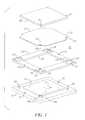
- FIG. 1is an exploded view of an alignment device for deposition mask in accordance with the present invention
- FIG. 2is a top view the alignment device of FIG. 1;
- FIG. 3is a cross-sectional view taken along lines 3 — 3 of FIG. 2;
- FIG. 4depicts a frame of another embodiment of the invention which includes a plurality of magnets
- FIG. 5is a schematic representation of the deposition of organic material onto a substrate of an OLED through the deposition mask which has been positioned relative to the substrate.
- FIG. 1depicts an exploded view of an alignment device 10 for a deposition mask 12 .
- the alignment device 10permits the deposition mask 12 to be positioned relative to a substrate of an OLED device to facilitate deposition.
- the alignment device 10includes a base 14 having a first set of alignment pins 16 and a second set of alignment pins 18 .
- the alignment pins 16 as showninclude two pins disposed on opposite sides of the base 14 .
- the base 14is generally rectangular and the second set of alignment pins 18 are disposed in three comers of the base 14 . As shown, in one of the comers there are two alignment pins 18 a and 18 b but in the remaining two comers there is a single alignment pin 18 .
- a plate 20is secured to the base 14 by any convenient means. As shown, the plate 20 is fastened by screws to the base 14 . Although the screws are not shown for convenience of illustration are depicted by holes 15 .
- the plate 20is preferably made of aluminum and provides a top flat surface on which the deposition mask 12 is to be positioned.
- a frame 22generally rectangular in shape, has a central opening 24 . Around each of the four comers of the frame 22 there are cutout portions 26 . In three of the cutout portions 26 , the alignment pins 18 project therethrough (see FIG. 2.)
- cutout portions 26are to facilitate positioning of the alignment device 10 in a vacuum chamber which permits the engagement of a mechanism in the vacuum chamber as well understood in the art.
- the frame 22is removably mounted to the base 14 using alignment pins 16 .
- the alignment pins 16pass through holes 17 a and 17 b in the frame 22 .
- the hole 17 ahas a circular 30 cross-section and holel 7 b has an oblong shape to permit proper alignment.
- a transparent flat plate 28is positioned to contact the second set of alignment pins 18 and deposition mask 12 and is sized to expose edge portions of the deposition mask 12 when it is properly positioned.
- the transparent flat plate 28includes fiducial marks 21 which are electroplated.
- the fiducial marks 21are cross lines which are shown larger than they actually are.
- the fiducial marks 21are used to permit a visual alignment with fiducial marks 23 on the deposition mask 12 .
- the exposed portions of the deposition mask 12is secured to the frame 22 . It can be secured by adhesive
- FIGS. 2 and 3respectively show a top view of the alignment device 10 and a cross-sectional view taken along lines 3 — 3 .
- the base 14 , plate 20 , the deposition mask 12 and the transparent flat plate 28are shown stacked one on top of the other.
- the frame 22is shown to have the same width as plate 20 .
- the pins 16 and 18are not shown for clarity of illustration. One of the pins 18 is shown in its alignment position.
- the alignment of the deposition mask 12 in the alignment device 10will now be described.
- the frame 22is mounted on base 14 using alignment pins 16 .
- the alignment pins 16are located on the base 14 in such a manner that frame 22 can be mounted in one orientation only.
- the frame 22 when mounted on base 14is to be positioned in a manner that aligns plate 20 top surface is at the same identical height as frame 22 .
- the deposition mask 12is visually aligned on top of plate 20 and frame 22 using engraved alignment lines 19 on frame 22 for initial alignment as shown in FIG. 1 .
- the transparent flat plate 28is placed on top of deposition mask 12 and against alignment pins 18 , 18 a , and 18 b .
- the deposition mask 12is manually aligned using the electroplated fiducial 23 and corresponding fiducial 21 located on transparent flat plate 28 .
- the relationship of transparent flat plate 28 and alignment pins 18 , 18 a , and 18 bmust remain against the alignment pins 18 a and 18 b during the alignment process.
- Deposition mask 12is then attached to frame 22 using one of two methods.
- adhesive strips 25secure the deposition mask 12 the frame 22 . Only one of the adhesive strips 25 is shown although typically there will be two for each edge and they secure the deposition mask 12 to frame 22 .
- the alignment device 10is the same as in FIGS. 1-3 with the exception that a plurality of magnets 30 are deposed around the periphery of the frame 22 .
- the deposition maskis made to include magnetic material for example ferrous metals such as nickel cobalt as well other materials.
- the amount of ferrous metalsis such that the field exerted by the magnets 30 causes the deposition mask 12 to be secured to the frame 22 and held in a planar fashion.
- the second methodis particularly suitable when it is not desirable to use adhesives. Both the first and second methods can however be simultaneously used in certain applications.
- FIG. 5is a schematic representation of the deposition of organic material onto a substrate 32 of an OLED device through the deposition mask 12 .
- the transparent flat plate 28is removed.
- the assembled deposition mask 12 and frame 22are removed from base 14 . It is the assembled deposition mask 12 and frame 22 are placed in an evacuation chamber (not shown).
- the substrate 32is positioned on the deposition mask 12 .
- a flat plate magnet 34is placed on the substrate 32 and exerts a magnetic field which pulls the deposition mask 12 into the substrate 32 .
- a deposition sourceapplies heat to organic material which is evaporate and deposited through the deposition mask 12 onto the substrate 32 .
Landscapes
- Engineering & Computer Science (AREA)
- Chemical & Material Sciences (AREA)
- Manufacturing & Machinery (AREA)
- Chemical Kinetics & Catalysis (AREA)
- Materials Engineering (AREA)
- Mechanical Engineering (AREA)
- Metallurgy (AREA)
- Organic Chemistry (AREA)
- Electroluminescent Light Sources (AREA)
- Physical Vapour Deposition (AREA)
Abstract
Description
| 10 | |||
| 12 | |||
| cutout portions | |||
| 14 | |||
| 15 | |||
| 16 | |||
| 17a | holes | ||
| 17b | holes | ||
| 18 | |||
| 18a | alignment pins | ||
| 18b | alignment pins | ||
| 19 | |||
| 20 | |||
| 21 | |||
| 22 | |||
| 23 | |||
| 24 | |||
| 25 | |||
| 26 | |||
| 28 | transparent | ||
| 32 | |||
| 34 | flat plate magnet | ||
Claims (6)
Priority Applications (5)
| Application Number | Priority Date | Filing Date | Title |
|---|---|---|---|
| US09/893,250US6475287B1 (en) | 2001-06-27 | 2001-06-27 | Alignment device which facilitates deposition of organic material through a deposition mask |
| TW091109344ATW569306B (en) | 2001-06-27 | 2002-05-06 | Alignment device which facilitates deposition of organic material through a deposition mask |
| EP02077367AEP1276160A3 (en) | 2001-06-27 | 2002-06-17 | Alignment device which facilitates deposition of organic material through a deposition mask |
| KR1020020036087AKR20030004073A (en) | 2001-06-27 | 2002-06-26 | Alignment device which facilitates deposition of organic material through a deposition mask |
| JP2002185579AJP4216531B2 (en) | 2001-06-27 | 2002-06-26 | Alignment device and organic material vapor deposition method |
Applications Claiming Priority (1)
| Application Number | Priority Date | Filing Date | Title |
|---|---|---|---|
| US09/893,250US6475287B1 (en) | 2001-06-27 | 2001-06-27 | Alignment device which facilitates deposition of organic material through a deposition mask |
Publications (1)
| Publication Number | Publication Date |
|---|---|
| US6475287B1true US6475287B1 (en) | 2002-11-05 |
Family
ID=25401265
Family Applications (1)
| Application Number | Title | Priority Date | Filing Date |
|---|---|---|---|
| US09/893,250Expired - LifetimeUS6475287B1 (en) | 2001-06-27 | 2001-06-27 | Alignment device which facilitates deposition of organic material through a deposition mask |
Country Status (5)
| Country | Link |
|---|---|
| US (1) | US6475287B1 (en) |
| EP (1) | EP1276160A3 (en) |
| JP (1) | JP4216531B2 (en) |
| KR (1) | KR20030004073A (en) |
| TW (1) | TW569306B (en) |
Cited By (45)
| Publication number | Priority date | Publication date | Assignee | Title |
|---|---|---|---|---|
| US20030012981A1 (en)* | 2001-06-29 | 2003-01-16 | Tsutomu Yamada | Method of manufacturing electroluminescence display apparatus |
| US20030017259A1 (en)* | 2001-06-29 | 2003-01-23 | Tsutomu Yamada | Method of manufacturing electroluminescence display apparatus |
| US20030017258A1 (en)* | 2001-06-29 | 2003-01-23 | Tsutomu Yamada | Method of manufacturing electroluminescence display apparatus |
| US20030101932A1 (en)* | 2001-12-05 | 2003-06-05 | Samsung Nec Mobile Display Co., Ltd. | Tension mask assembly for use in vacuum deposition of thin film of organic electroluminescent device |
| US20030108805A1 (en)* | 2001-12-10 | 2003-06-12 | Eastman Kodak Company | Aligning mask segments to provide an assembled mask for producing oled devices |
| US6589382B2 (en)* | 2001-11-26 | 2003-07-08 | Eastman Kodak Company | Aligning mask segments to provide a stitched mask for producing OLED devices |
| US20030201711A1 (en)* | 2002-04-26 | 2003-10-30 | Tohoku Pioneer Corporation | Mask for vacuum deposition and organic EL display manufactured by using the same |
| US20030221614A1 (en)* | 2002-06-03 | 2003-12-04 | Samsung Nec Mobile Display Co., Ltd., Ulsan-City, Republic Of Korea | Mask and mask frame assembly for evaporation |
| US20040020435A1 (en)* | 2001-08-24 | 2004-02-05 | Terunoa Tsuchiya | Multi-face forming mask device for vacuum deposition |
| US20040091251A1 (en)* | 2002-10-25 | 2004-05-13 | Chun-An Chen | Evaporation method and apparatus thereof |
| US20040123799A1 (en)* | 2002-12-31 | 2004-07-01 | Eastman Kodak Company | Flexible frame for mounting a deposition mask |
| US20050034810A1 (en)* | 2003-04-10 | 2005-02-17 | Semiconductor Energy Laboratory Co., Ltd. | Mask and container and manufacturing apparatus |
| US20050287897A1 (en)* | 2004-06-25 | 2005-12-29 | Chi Mei Optoelectronics Corp. | Method of producing display using mask alignment method |
| US20060086609A1 (en)* | 2004-10-22 | 2006-04-27 | Taiwan Semiconductor Manufacturing Co., Ltd. | Current-leveling electroplating/electropolishing electrode |
| US20060086321A1 (en)* | 2004-10-22 | 2006-04-27 | Advantech Global, Ltd | Substrate-to-mask alignment and securing system with temperature control for use in an automated shadow mask vacuum deposition process |
| US20070137568A1 (en)* | 2005-12-16 | 2007-06-21 | Schreiber Brian E | Reciprocating aperture mask system and method |
| US20070163494A1 (en)* | 2005-12-28 | 2007-07-19 | Tokie Jeffrey H | Rotatable aperture mask assembly and deposition system |
| US20070190889A1 (en)* | 2006-02-16 | 2007-08-16 | Samsung Electronics Co., Ltd. | Mask and method of manufacturing the same |
| US20080127490A1 (en)* | 2006-12-01 | 2008-06-05 | Lotes Co., Ltd. | Manufacture process of connector |
| US20080150414A1 (en)* | 2006-12-26 | 2008-06-26 | Samsung Electronics Co., Ltd. | Shadow mask apparatus and manufacturing method of organic electroluminescent display using the same |
| US20090159432A1 (en)* | 2006-08-28 | 2009-06-25 | Mitsubishi Heavy Industries, Ltd. | Thin-film deposition apparatus using discharge electrode and solar cell fabrication method |
| US20090203283A1 (en)* | 2008-02-07 | 2009-08-13 | Margaret Helen Gentile | Method for sealing an electronic device |
| CN1916228B (en)* | 2005-07-20 | 2010-06-09 | 精工爱普生株式会社 | Mask and its manufacturing method, film forming method, and manufacturing method of electro-optical device |
| CN101090997B (en)* | 2005-02-23 | 2010-11-24 | 三井造船株式会社 | Mask aligning mechanism for film forming apparatus, and film forming apparatus |
| CN101969105A (en)* | 2010-11-12 | 2011-02-09 | 四川虹视显示技术有限公司 | Substrate and evaporation method thereof |
| US20110185965A1 (en)* | 2010-02-03 | 2011-08-04 | Chong-Hyun Park | Mask assembly |
| CN102651457A (en)* | 2011-04-28 | 2012-08-29 | 京东方科技集团股份有限公司 | Fixing device of substrate and fixing method based on device |
| US8273179B2 (en) | 2003-03-27 | 2012-09-25 | Samsung Mobile Display Co., Ltd. | Deposition mask for display device and method for fabricating the same |
| CN102780467A (en)* | 2012-08-03 | 2012-11-14 | 南京中电熊猫晶体科技有限公司 | Mask plate for coating film in initial plating process of high-fundamental frequency Invert Mesa crystal plate |
| CN102856346A (en)* | 2011-06-14 | 2013-01-02 | 三星显示有限公司 | Method of manufacturing organic light-emitting display apparatus |
| US20130276978A1 (en)* | 2012-04-19 | 2013-10-24 | Intevac, Inc. | Dual-mask arrangement for solar cell fabrication |
| CN103962719A (en)* | 2013-02-01 | 2014-08-06 | 三星显示有限公司 | Mask manufacturing apparatus and method of manufacturing mask using laser beam |
| US20140326780A1 (en)* | 2013-05-02 | 2014-11-06 | Samsung Display Co,. Ltd. | Welding device for mask frame assembly and method of welding mask frame assembly |
| US8993360B2 (en) | 2013-03-29 | 2015-03-31 | Samsung Display Co., Ltd. | Deposition apparatus, method of manufacturing organic light emitting display apparatus, and organic light emitting display apparatus |
| DE102005005124B4 (en)* | 2005-02-04 | 2015-07-23 | Robert Bosch Gmbh | Method of aligning a plurality of substrates onto an exposure mask |
| WO2016061215A1 (en)* | 2014-10-17 | 2016-04-21 | Advantech Global, Ltd | Multi-mask alignment system and method |
| US9502276B2 (en) | 2012-04-26 | 2016-11-22 | Intevac, Inc. | System architecture for vacuum processing |
| US9543114B2 (en) | 2014-08-05 | 2017-01-10 | Intevac, Inc. | Implant masking and alignment system with rollers |
| US9825014B2 (en)* | 2015-11-19 | 2017-11-21 | Samsung Electronics Co., Ltd. | Light source module, display panel, and display apparatus including the same |
| US10062600B2 (en) | 2012-04-26 | 2018-08-28 | Intevac, Inc. | System and method for bi-facial processing of substrates |
| WO2018209612A1 (en)* | 2017-05-17 | 2018-11-22 | 深圳市柔宇科技有限公司 | Contact plate, alignment system, and vapor deposition device |
| US20190003033A1 (en)* | 2016-06-29 | 2019-01-03 | Boe Technology Group Co., Ltd. | Mask plate and method for manufacturing the same |
| US20210324508A1 (en)* | 2020-04-17 | 2021-10-21 | Rockwell Collins, Inc. | Additively manufactured shadow masks for material deposition control |
| US20220081753A1 (en)* | 2020-09-11 | 2022-03-17 | Samsung Display Co., Ltd. | Deposition apparatus and method for seating mask of deposition apparatus |
| US20240138245A1 (en)* | 2021-02-05 | 2024-04-25 | Samsung Display Co., Ltd. | Mask and method of manufacturing the same |
Families Citing this family (11)
| Publication number | Priority date | Publication date | Assignee | Title |
|---|---|---|---|---|
| KR100671656B1 (en) | 2005-01-05 | 2007-01-19 | 삼성에스디아이 주식회사 | Tray Alignment |
| KR100703544B1 (en) | 2005-01-05 | 2007-04-03 | 삼성에스디아이 주식회사 | Tray Alignment |
| JP4375232B2 (en)* | 2005-01-06 | 2009-12-02 | セイコーエプソン株式会社 | Mask deposition method |
| KR100657027B1 (en)* | 2005-02-07 | 2006-12-13 | 재단법인서울대학교산학협력재단 | Improved packaging adhesive tape with temperature sensing |
| KR100898395B1 (en)* | 2007-09-28 | 2009-05-21 | 세메스 주식회사 | Substrate Alignment Device and Method |
| TWI475736B (en)* | 2011-07-26 | 2015-03-01 | Innolux Corp | Manufacturing method of electroluminescent display apparatus and plating machine |
| KR102080480B1 (en) | 2012-12-27 | 2020-02-24 | 엘지디스플레이 주식회사 | Substrate-clamping unit and apparatus for depositing organic material using the same |
| JP5568683B2 (en)* | 2013-12-25 | 2014-08-06 | 株式会社半導体エネルギー研究所 | Vapor deposition mask and vapor deposition method using the mask |
| JP6511908B2 (en)* | 2014-03-31 | 2019-05-15 | 大日本印刷株式会社 | Tension method of deposition mask, method of manufacturing deposition mask with frame, method of manufacturing organic semiconductor device, and tension device |
| JP6844646B2 (en)* | 2014-03-31 | 2021-03-17 | 大日本印刷株式会社 | Deposition mask tension method, framed vapor deposition mask manufacturing method, organic semiconductor device manufacturing method, and tensioning device |
| JP7133383B2 (en)* | 2018-07-31 | 2022-09-08 | マクセル株式会社 | Evaporation mask |
Citations (1)
| Publication number | Priority date | Publication date | Assignee | Title |
|---|---|---|---|---|
| US6146489A (en)* | 1998-11-19 | 2000-11-14 | General Electric Company | Method and apparatus for depositing scintillator material on radiation imager |
Family Cites Families (2)
| Publication number | Priority date | Publication date | Assignee | Title |
|---|---|---|---|---|
| US4511599A (en)* | 1983-03-01 | 1985-04-16 | Sigmatron Associates | Mask for vacuum depositing back metal electrodes on EL panel |
| US4915057A (en)* | 1985-10-23 | 1990-04-10 | Gte Products Corporation | Apparatus and method for registration of shadow masked thin-film patterns |
- 2001
- 2001-06-27USUS09/893,250patent/US6475287B1/ennot_activeExpired - Lifetime
- 2002
- 2002-05-06TWTW091109344Apatent/TW569306B/ennot_activeIP Right Cessation
- 2002-06-17EPEP02077367Apatent/EP1276160A3/ennot_activeWithdrawn
- 2002-06-26JPJP2002185579Apatent/JP4216531B2/ennot_activeExpired - Lifetime
- 2002-06-26KRKR1020020036087Apatent/KR20030004073A/ennot_activeWithdrawn
Patent Citations (1)
| Publication number | Priority date | Publication date | Assignee | Title |
|---|---|---|---|---|
| US6146489A (en)* | 1998-11-19 | 2000-11-14 | General Electric Company | Method and apparatus for depositing scintillator material on radiation imager |
Cited By (73)
| Publication number | Priority date | Publication date | Assignee | Title |
|---|---|---|---|---|
| US20030017259A1 (en)* | 2001-06-29 | 2003-01-23 | Tsutomu Yamada | Method of manufacturing electroluminescence display apparatus |
| US20030017258A1 (en)* | 2001-06-29 | 2003-01-23 | Tsutomu Yamada | Method of manufacturing electroluminescence display apparatus |
| US20030012981A1 (en)* | 2001-06-29 | 2003-01-16 | Tsutomu Yamada | Method of manufacturing electroluminescence display apparatus |
| US6827622B2 (en)* | 2001-06-29 | 2004-12-07 | Sanyo Electric Co., Ltd. | Method of manufacturing electroluminescence display apparatus |
| US20040020435A1 (en)* | 2001-08-24 | 2004-02-05 | Terunoa Tsuchiya | Multi-face forming mask device for vacuum deposition |
| US6890385B2 (en)* | 2001-08-24 | 2005-05-10 | Dai Nippon Printing Co., Ltd. | Multi-face forming mask device for vacuum deposition |
| US6589382B2 (en)* | 2001-11-26 | 2003-07-08 | Eastman Kodak Company | Aligning mask segments to provide a stitched mask for producing OLED devices |
| US6858086B2 (en)* | 2001-12-05 | 2005-02-22 | Samsung Oled Co., Ltd. | Tension mask assembly for use in vacuum deposition of thin film of organic electroluminescent device |
| US20030101932A1 (en)* | 2001-12-05 | 2003-06-05 | Samsung Nec Mobile Display Co., Ltd. | Tension mask assembly for use in vacuum deposition of thin film of organic electroluminescent device |
| US20030108805A1 (en)* | 2001-12-10 | 2003-06-12 | Eastman Kodak Company | Aligning mask segments to provide an assembled mask for producing oled devices |
| US6749690B2 (en)* | 2001-12-10 | 2004-06-15 | Eastman Kodak Company | Aligning mask segments to provide an assembled mask for producing OLED devices |
| US20030201711A1 (en)* | 2002-04-26 | 2003-10-30 | Tohoku Pioneer Corporation | Mask for vacuum deposition and organic EL display manufactured by using the same |
| US6878208B2 (en)* | 2002-04-26 | 2005-04-12 | Tohoku Pioneer Corporation | Mask for vacuum deposition and organic EL display manufactured by using the same |
| US20050098110A1 (en)* | 2002-04-26 | 2005-05-12 | Tohoku Pioneer Corporation | Mask for vacuum deposition and organic EL display panel manufactured by using the same |
| US20030221614A1 (en)* | 2002-06-03 | 2003-12-04 | Samsung Nec Mobile Display Co., Ltd., Ulsan-City, Republic Of Korea | Mask and mask frame assembly for evaporation |
| US6955726B2 (en)* | 2002-06-03 | 2005-10-18 | Samsung Sdi Co., Ltd. | Mask and mask frame assembly for evaporation |
| US7125581B2 (en)* | 2002-10-25 | 2006-10-24 | Ritdisplay Corporation | Evaporation method and apparatus thereof |
| US20040091251A1 (en)* | 2002-10-25 | 2004-05-13 | Chun-An Chen | Evaporation method and apparatus thereof |
| US20040123799A1 (en)* | 2002-12-31 | 2004-07-01 | Eastman Kodak Company | Flexible frame for mounting a deposition mask |
| WO2004061149A1 (en)* | 2002-12-31 | 2004-07-22 | Eastman Kodak Company | Flexible frame for mounting a deposition mask |
| US6926840B2 (en) | 2002-12-31 | 2005-08-09 | Eastman Kodak Company | Flexible frame for mounting a deposition mask |
| US8273179B2 (en) | 2003-03-27 | 2012-09-25 | Samsung Mobile Display Co., Ltd. | Deposition mask for display device and method for fabricating the same |
| US20050034810A1 (en)* | 2003-04-10 | 2005-02-17 | Semiconductor Energy Laboratory Co., Ltd. | Mask and container and manufacturing apparatus |
| CN1621555B (en)* | 2003-04-10 | 2011-06-15 | 株式会社半导体能源研究所 | Masks, containers and fabrication devices |
| US20090170227A1 (en)* | 2003-04-10 | 2009-07-02 | Semiconductor Energy Laboratory Co., Ltd. | Mask and container and manufacturing |
| US20050287897A1 (en)* | 2004-06-25 | 2005-12-29 | Chi Mei Optoelectronics Corp. | Method of producing display using mask alignment method |
| US20060086321A1 (en)* | 2004-10-22 | 2006-04-27 | Advantech Global, Ltd | Substrate-to-mask alignment and securing system with temperature control for use in an automated shadow mask vacuum deposition process |
| US20060086609A1 (en)* | 2004-10-22 | 2006-04-27 | Taiwan Semiconductor Manufacturing Co., Ltd. | Current-leveling electroplating/electropolishing electrode |
| WO2006047305A3 (en)* | 2004-10-22 | 2007-05-31 | Advantech Global Ltd | Substrate-to-mask alignment and securing system |
| US7803257B2 (en)* | 2004-10-22 | 2010-09-28 | Taiwan Semiconductor Manufacturing Company | Current-leveling electroplating/electropolishing electrode |
| DE102005005124B4 (en)* | 2005-02-04 | 2015-07-23 | Robert Bosch Gmbh | Method of aligning a plurality of substrates onto an exposure mask |
| CN101090997B (en)* | 2005-02-23 | 2010-11-24 | 三井造船株式会社 | Mask aligning mechanism for film forming apparatus, and film forming apparatus |
| CN1916228B (en)* | 2005-07-20 | 2010-06-09 | 精工爱普生株式会社 | Mask and its manufacturing method, film forming method, and manufacturing method of electro-optical device |
| US20070137568A1 (en)* | 2005-12-16 | 2007-06-21 | Schreiber Brian E | Reciprocating aperture mask system and method |
| US20070163494A1 (en)* | 2005-12-28 | 2007-07-19 | Tokie Jeffrey H | Rotatable aperture mask assembly and deposition system |
| US7763114B2 (en) | 2005-12-28 | 2010-07-27 | 3M Innovative Properties Company | Rotatable aperture mask assembly and deposition system |
| US20070190889A1 (en)* | 2006-02-16 | 2007-08-16 | Samsung Electronics Co., Ltd. | Mask and method of manufacturing the same |
| US20090159432A1 (en)* | 2006-08-28 | 2009-06-25 | Mitsubishi Heavy Industries, Ltd. | Thin-film deposition apparatus using discharge electrode and solar cell fabrication method |
| US20080127490A1 (en)* | 2006-12-01 | 2008-06-05 | Lotes Co., Ltd. | Manufacture process of connector |
| US20080150414A1 (en)* | 2006-12-26 | 2008-06-26 | Samsung Electronics Co., Ltd. | Shadow mask apparatus and manufacturing method of organic electroluminescent display using the same |
| US20090203283A1 (en)* | 2008-02-07 | 2009-08-13 | Margaret Helen Gentile | Method for sealing an electronic device |
| US20110185965A1 (en)* | 2010-02-03 | 2011-08-04 | Chong-Hyun Park | Mask assembly |
| US9004002B2 (en)* | 2010-02-03 | 2015-04-14 | Lg Display Co., Ltd. | Mask assembly having a plurality of projections at a boundary of adjacent two deposition masks |
| CN101969105B (en)* | 2010-11-12 | 2012-09-19 | 四川虹视显示技术有限公司 | Substrate and evaporation method thereof |
| CN101969105A (en)* | 2010-11-12 | 2011-02-09 | 四川虹视显示技术有限公司 | Substrate and evaporation method thereof |
| CN102651457A (en)* | 2011-04-28 | 2012-08-29 | 京东方科技集团股份有限公司 | Fixing device of substrate and fixing method based on device |
| CN102856346A (en)* | 2011-06-14 | 2013-01-02 | 三星显示有限公司 | Method of manufacturing organic light-emitting display apparatus |
| CN102856346B (en)* | 2011-06-14 | 2016-09-07 | 三星显示有限公司 | The method manufacturing organic light-emitting display device |
| US20130276978A1 (en)* | 2012-04-19 | 2013-10-24 | Intevac, Inc. | Dual-mask arrangement for solar cell fabrication |
| US9525099B2 (en)* | 2012-04-19 | 2016-12-20 | Intevac, Inc. | Dual-mask arrangement for solar cell fabrication |
| US9502276B2 (en) | 2012-04-26 | 2016-11-22 | Intevac, Inc. | System architecture for vacuum processing |
| US10062600B2 (en) | 2012-04-26 | 2018-08-28 | Intevac, Inc. | System and method for bi-facial processing of substrates |
| CN102780467A (en)* | 2012-08-03 | 2012-11-14 | 南京中电熊猫晶体科技有限公司 | Mask plate for coating film in initial plating process of high-fundamental frequency Invert Mesa crystal plate |
| US9377681B2 (en)* | 2013-02-01 | 2016-06-28 | Samsung Display Co., Ltd. | Mask manufacturing apparatus and method of manufacturing mask using laser beam |
| US20140217646A1 (en)* | 2013-02-01 | 2014-08-07 | Samsung Display Co., Ltd. | Mask manufacturing apparatus and method of manufacturing mask using laser beam |
| TWI620976B (en)* | 2013-02-01 | 2018-04-11 | 三星顯示器有限公司 | Mask manufacturing apparatus and method of manufacturing mask using laser beam |
| CN103962719A (en)* | 2013-02-01 | 2014-08-06 | 三星显示有限公司 | Mask manufacturing apparatus and method of manufacturing mask using laser beam |
| CN103962719B (en)* | 2013-02-01 | 2017-04-12 | 三星显示有限公司 | Mask manufacturing apparatus and method of manufacturing mask using laser beam |
| US8993360B2 (en) | 2013-03-29 | 2015-03-31 | Samsung Display Co., Ltd. | Deposition apparatus, method of manufacturing organic light emitting display apparatus, and organic light emitting display apparatus |
| US20140326780A1 (en)* | 2013-05-02 | 2014-11-06 | Samsung Display Co,. Ltd. | Welding device for mask frame assembly and method of welding mask frame assembly |
| US9543114B2 (en) | 2014-08-05 | 2017-01-10 | Intevac, Inc. | Implant masking and alignment system with rollers |
| WO2016061215A1 (en)* | 2014-10-17 | 2016-04-21 | Advantech Global, Ltd | Multi-mask alignment system and method |
| US10323316B2 (en) | 2014-10-17 | 2019-06-18 | Advantech Global, Ltd | Multi-mask alignment system and method |
| US9825014B2 (en)* | 2015-11-19 | 2017-11-21 | Samsung Electronics Co., Ltd. | Light source module, display panel, and display apparatus including the same |
| US20190003033A1 (en)* | 2016-06-29 | 2019-01-03 | Boe Technology Group Co., Ltd. | Mask plate and method for manufacturing the same |
| US10787729B2 (en)* | 2016-06-29 | 2020-09-29 | Boe Technology Group Co., Ltd. | Mask plate and method for manufacturing the same |
| US11396693B2 (en) | 2016-06-29 | 2022-07-26 | Ordos Yuansheng Optoelectronics Co., Ltd. | Mask plate and method for manufacturing the same |
| WO2018209612A1 (en)* | 2017-05-17 | 2018-11-22 | 深圳市柔宇科技有限公司 | Contact plate, alignment system, and vapor deposition device |
| US20210324508A1 (en)* | 2020-04-17 | 2021-10-21 | Rockwell Collins, Inc. | Additively manufactured shadow masks for material deposition control |
| US11613802B2 (en)* | 2020-04-17 | 2023-03-28 | Rockwell Collins, Inc. | Additively manufactured shadow masks for material deposition control |
| US20220081753A1 (en)* | 2020-09-11 | 2022-03-17 | Samsung Display Co., Ltd. | Deposition apparatus and method for seating mask of deposition apparatus |
| US12428717B2 (en)* | 2020-09-11 | 2025-09-30 | Samsung Display Co., Ltd. | Deposition apparatus and method for seating mask of deposition apparatus |
| US20240138245A1 (en)* | 2021-02-05 | 2024-04-25 | Samsung Display Co., Ltd. | Mask and method of manufacturing the same |
Also Published As
| Publication number | Publication date |
|---|---|
| KR20030004073A (en) | 2003-01-14 |
| EP1276160A3 (en) | 2007-11-14 |
| TW569306B (en) | 2004-01-01 |
| JP2003100456A (en) | 2003-04-04 |
| EP1276160A2 (en) | 2003-01-15 |
| JP4216531B2 (en) | 2009-01-28 |
Similar Documents
| Publication | Publication Date | Title |
|---|---|---|
| US6475287B1 (en) | Alignment device which facilitates deposition of organic material through a deposition mask | |
| US6589382B2 (en) | Aligning mask segments to provide a stitched mask for producing OLED devices | |
| US6749690B2 (en) | Aligning mask segments to provide an assembled mask for producing OLED devices | |
| US6926840B2 (en) | Flexible frame for mounting a deposition mask | |
| US4915057A (en) | Apparatus and method for registration of shadow masked thin-film patterns | |
| US4746548A (en) | Method for registration of shadow masked thin-film patterns | |
| US20040021410A1 (en) | Method and apparatus for making a shadow mask array | |
| CN108977762B (en) | Mask plate, suit mask plate and coating by vaporization system | |
| TWI467679B (en) | Chip stack device testing method, chip stack device rearranging unit, and chip stack device testing apparatus | |
| CN106544638B (en) | A kind of mask panel assembly of assembling-type | |
| JPH1060624A (en) | Sputtering equipment | |
| US20070049064A1 (en) | Alignment precision enhancement of electronic component process on flexible substrate device and method thereof the same | |
| KR20220016383A (en) | Mask and manufacturing method of mask | |
| US4563085A (en) | Method of producing lithographic plates | |
| US4529303A (en) | Apparatus for producing lithographic plates | |
| CN119287333A (en) | A combined fixture for filter sputtering coating and assembly method thereof | |
| CN119265520A (en) | A mask device | |
| CN110249071A (en) | Deposition mask fixes device | |
| JPH0877612A (en) | Film forming mask apparatus | |
| JPS63311355A (en) | Positioning method for pattern film to film molding substrate | |
| JPH08330400A (en) | Air chuck unit mounting structure |
Legal Events
| Date | Code | Title | Description |
|---|---|---|---|
| AS | Assignment | Owner name:EASTMAN KODAK COMPANY, NEW YORK Free format text:ASSIGNMENT OF ASSIGNORS INTEREST;ASSIGNOR:CLARK, THOMAS K.;REEL/FRAME:011951/0693 Effective date:20010625 | |
| STCF | Information on status: patent grant | Free format text:PATENTED CASE | |
| FEPP | Fee payment procedure | Free format text:PAYOR NUMBER ASSIGNED (ORIGINAL EVENT CODE: ASPN); ENTITY STATUS OF PATENT OWNER: LARGE ENTITY | |
| AS | Assignment | Owner name:NIHON DEMPA KOGYO CO., LTD., JAPAN Free format text:ASSIGNMENT OF ASSIGNORS INTEREST;ASSIGNOR:NRS TECHNOLOGIES, INC.;REEL/FRAME:017403/0135 Effective date:20050915 | |
| FPAY | Fee payment | Year of fee payment:4 | |
| FEPP | Fee payment procedure | Free format text:PAYER NUMBER DE-ASSIGNED (ORIGINAL EVENT CODE: RMPN); ENTITY STATUS OF PATENT OWNER: LARGE ENTITY Free format text:PAYOR NUMBER ASSIGNED (ORIGINAL EVENT CODE: ASPN); ENTITY STATUS OF PATENT OWNER: LARGE ENTITY | |
| AS | Assignment | Owner name:GLOBAL OLED TECHNOLOGY LLC,DELAWARE Free format text:ASSIGNMENT OF ASSIGNORS INTEREST;ASSIGNOR:EASTMAN KODAK COMPANY;REEL/FRAME:023998/0368 Effective date:20100122 Owner name:GLOBAL OLED TECHNOLOGY LLC, DELAWARE Free format text:ASSIGNMENT OF ASSIGNORS INTEREST;ASSIGNOR:EASTMAN KODAK COMPANY;REEL/FRAME:023998/0368 Effective date:20100122 | |
| FPAY | Fee payment | Year of fee payment:8 | |
| FPAY | Fee payment | Year of fee payment:12 |