US6473825B1 - Apparatus and method for controlling secure communications between peripheral components on computer buses connected by a bridge circuit - Google Patents
Apparatus and method for controlling secure communications between peripheral components on computer buses connected by a bridge circuitDownload PDFInfo
- Publication number
- US6473825B1 US6473825B1US09/481,331US48133100AUS6473825B1US 6473825 B1US6473825 B1US 6473825B1US 48133100 AUS48133100 AUS 48133100AUS 6473825 B1US6473825 B1US 6473825B1
- Authority
- US
- United States
- Prior art keywords
- address
- peripheral component
- message
- bus
- permitted
- Prior art date
- Legal status (The legal status is an assumption and is not a legal conclusion. Google has not performed a legal analysis and makes no representation as to the accuracy of the status listed.)
- Expired - Lifetime
Links
Images


Classifications
- G—PHYSICS
- G06—COMPUTING OR CALCULATING; COUNTING
- G06F—ELECTRIC DIGITAL DATA PROCESSING
- G06F21/00—Security arrangements for protecting computers, components thereof, programs or data against unauthorised activity
- G06F21/70—Protecting specific internal or peripheral components, in which the protection of a component leads to protection of the entire computer
- G06F21/82—Protecting input, output or interconnection devices
- G06F21/85—Protecting input, output or interconnection devices interconnection devices, e.g. bus-connected or in-line devices
- G—PHYSICS
- G06—COMPUTING OR CALCULATING; COUNTING
- G06F—ELECTRIC DIGITAL DATA PROCESSING
- G06F13/00—Interconnection of, or transfer of information or other signals between, memories, input/output devices or central processing units
- G06F13/38—Information transfer, e.g. on bus
- G06F13/40—Bus structure
- G06F13/4004—Coupling between buses
- G06F13/4027—Coupling between buses using bus bridges
- G06F13/4031—Coupling between buses using bus bridges with arbitration
Definitions
- the present inventionpertains to an apparatus for a method of controlling communication between peripheral components in a communication system. More particularly, the present invention pertains to an improved apparatus for and method of assuring that classified or sensitive messages are not transmitted to peripheral components which do not have the appropriate access authority to receive the messages.
- the present inventionis a apparatus for and method of controlling communication between peripheral components in a secure communication system.
- the present inventionpermits use of commercial, off-the-shelf operating systems and processors, since it is not necessary to alter the operating systems or processors to permit secure communication of messages.
- the sensitivity level of each peripheral component address in the communication systemis fixed.
- the addresses of the originating peripheral component and the destination peripheral componentare detected, and it is then determined whether the address of the destination peripheral component is an address to which a peripheral component at the originating address is permitted to communicate.
- the destination addressmust have a sensitivity level equal to or greater than the sensitivity level of the originating address. If not, then communication of further messages from the origination address is prevented, thereby preventing communication of messages of a particular sensitivity level to peripheral components of lower sensitivity level. If the address of the destination peripheral component is an address to which the peripheral component at the originating address is permitted to communicate, then communication of messages from the origination address is permitted to continue.
- the apparatus of the present inventionincludes a first address detector for detecting the address of the originating peripheral component, a second address detector for detecting the address of the destination peripheral component, and an address comparison circuit for determining whether the address of the destination peripheral component is an address to which a peripheral component at the originating address is permitted to communicate.
- the address comparison circuitis responsive to the address of the destination peripheral component not being an address to the which the peripheral component at the originating address is permitted to communicate by generating an error signal, preventing communication of further messages from the origination address. If the address of the destination peripheral component is an address to which the peripheral component at the originating address is permitted to communicate, transmission of messages from the origination address is permitted to continue.
- the originating and destination peripheral addressesmight be on the same communication bus. Alternatively, they might be on different buses connected by one or more bridge circuits.
- the bridge circuit on the bus of the originating addressdetects the destination address of messages originating at addresses on its bus and determines whether the destination address is an address to which the peripheral component at the originating address is permitted to send a message.
- the sensitively levelis always checked by the bridge circuit on the bus of the originating address. Consequently, no such check is necessary at the bus of the destination address.
- the present inventionis particularly applicable for use in communication within military aircraft. However, it is likewise usable in communication within other systems.
- FIG. 1is a block diagram of a preferred embodiment of an apparatus for controlling communication between peripheral component addresses in a communication system in accordance with the present invention
- FIG. 2is a block diagram of a preferred embodiment of a gateway unit suitable for incorporation into the apparatus of FIG. 1 in accordance with the present invention
- FIG. 3is a flowchart illustrating operation of the gateway unit of FIG. 2 in accordance with the present invention
- FIG. 4is a block diagram of a preferred embodiment of a bus arbiter and bridge circuit suitable for incorporation into the apparatus of FIG. 1 in accordance with the present invention
- FIG. 5is a flowchart illustrating operation of the bus arbiter and bridge circuit of FIG. 4 in accordance with the present invention
- FIG. 6is a block diagram of a preferred embodiment of cross-rack interface units suitable for incorporation into the apparatus of FIG. 1 in accordance with the present invention.
- FIG. 7is a flowchart illustrating operation of the cross-rack interface units of FIG. 6 in accordance with the present invention.
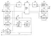
- FIG. 1is a block diagram of a communication system in accordance with a preferred embodiment of the present invention.
- the communication systemincludes a first data processing unit 10 which is coupled to a first control unit 12 .
- the first control unit 12is coupled to a second control unit 12 a which is coupled to additional data processing units, depicted in FIG. 1 as data processing units 10 a and 10 b , although additional data processing units could be connected to control unit 12 a , if desired.
- additional data processing unitscould be connected to control unit 12 a , if desired.
- more than one data processing unitcould be connected to control unit 12 .
- the several data processing units 10 , 10 a , 10 b , etc.are substantially identical, and so only the details of the data processing unit 10 are depicted in FIG. 1 and described in the following detailed description.
- Data processing unit 10can send and receive communications on bus 15 to and from input/output unit 14 , which, by way of example, might include one or more radio receivers or other equipment providing communication, navigation, and identification functions.
- bus 15connects input/output unit 14 to a gateway unit 16 .
- Communication bus 18connects gateway unit 16 to a plurality of processors within data processing unit 10 .
- FIG. 1illustrates communication bus 18 connected to processors 20 , 22 , and 24 ; however, any number of processors might be included.
- Communication bus 18is also connected to a cryptographic unit 26 and to a bus arbiter and bridge circuit 28 .
- Communication bus 18permits communication of both confidential or sensitive messages and non-sensitive messages among gateway unit 16 , processors 20 , 22 , 24 , etc., cryptographic unit 26 , and bus arbiter and bridge circuit 28 within data processing unit 10 .
- the processors 20 , 22 , 24 , etc.may be of identical design with identical operating systems.
- the address of each processoris assigned a sensitivity level, indicating the sensitivity level of messages a processor at that address is authorized to receive.
- FIG. 1illustratively depicts processor 20 as being at a “sensitivity level 2” address, processor 22 as being at a “sensitivity level 1” address, and processor 24 as being at a “sensitivity level 3” address, indicating that a processor at each of these addresses is authorized to receive messages having a sensitivity level up to the indicated level, but is not authorized to receive messages of a greater sensitivity level.
- Bus arbiter and bridge circuit 28has separate connections 30 a - 30 g to gateway unit 16 , to each of the processors 20 , 22 , 24 , etc., and to cryptographic unit 26 within data processing unit 10 .
- Cryptographic unit 26has a separate address on bus 18 for each sensitivity level, thus being depicted in FIG. 1 as having three connections to bus 18 , as well as three connections 30 e , 30 f , and 30 g to bus arbiter and bridge circuit 28 , separate ones for each of the sensitivity levels 1, 2, and 3 .
- FIG. 2is a block diagram of a preferred embodiment of gateway unit 16 within data processing unit 10
- FIG. 3illustrates its operation.
- the various signals which pass between input/output unit 14 and gateway unit 16either are not sensitive or are encrypted.
- Each received signalincludes, in addition to a message, a destination address indicating the intended destination of the message, and a token indicating the originating address of the message.
- the term “message”is sometimes used hereinafter to refer to the combination of the address, token, and message.
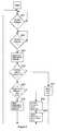
- the input signals on bus 15are applied at step S 1 to destination address detector 50 which detects the destination address. If destination address detector 50 determines at step S 2 that a received message is addressed to a destination for which communication does not pass through data processing unit 10 , then the process ends at step S 3 . If at step S 2 destination address detector 50 determines that the received message is addressed to a destination within data processing unit 10 , or to a destination for which communication passes through data processing unit 10 , then destination address detector 50 applies the message to buffer 52 .
- step S 4the message is reformatted, including reformatting the destination address in accordance with the address map of the system of FIG. 1 .
- Message formatting and sensitivity confirmation unit 54also detects the token within the message to determine the originating address and provides a sideband signal indicating the sensitivity level of that originating address.
- message formatting and sensitivity confirmation unit 54confirms that the destination address has the proper sensitivity level to receive a message from the originating address, thus assuring that no error occurred in the address reformatting to the address map of the system of FIG. 1 that would compromise confidentiality.
- step S 6message formatting and sensitivity level conformation unit 54 applies an error flag or message on line 55 to input/output unit 14 , and the process ends in step S 8 . If the destination address is confirmed to have the proper sensitivity level, then message formatting and sensitivity level confirmation unit 54 stores the reformatted message and sideband signal in buffer 58 . Output interface unit 60 then requests access to bus 18 , and when that access is granted passes the message and sideband signal from buffer 58 to communication bus 18 in step S 7 . The process then ends in step S 8 until receipt of the next message. Referring to FIGS.
- bus 18applies the message from output interface 60 to that processor. If the message is for a destination beyond data processing unit 10 , then bus 18 applies the message and sideband signal to bus arbiter and bridge circuit 28 for subsequent transmission.
- message formatting and sensitivity confirmation unit 54is connected to sensitivity level tables 56 which include a look-up table for each originating address from which communication can be received by gateway unit 16 .
- sensitivity level tables 56which include a look-up table for each originating address from which communication can be received by gateway unit 16 .
- Each look-up tablelists the addresses of peripheral units or other destinations to which the corresponding originating address is permitted to send communications, based on the sensitivity levels of the originating address and the destination address.
- Message formatting and sensitivity confirmation unit 54determines whether the destination address is on the look-up table of the originating address.
- step S 1when gateway unit 16 receives a message on bus 18 for transmission on bus 15 to input/output unit 14 , in step S 1 the message is received by destination address detector 62 which detects the message destination address. In step S 2 destination address detector 62 determines whether the destination address is an address for which communication is to pass through gateway unit 16 . If not, then in step S 3 , the process ends. If the message is to pass through gateway unit 16 , then the message is stored in buffer 64 , and in step S 4 message formatting and sensitivity level confirmation unit 66 reformats the message as necessary, determines the originating address, and consults the corresponding one of the sensitivity level look-up tables 68 to confirm in step S 5 that the destination address has the proper sensitivity level to receive the message.
- step S 6message formatting and sensitivity level confirmation unit 66 applies an error signal on line 67 to a maintenance processor 69 (FIG. 1) within data processing unit 10 , causing the maintenance processor to take appropriate action, such as applying a signal on bus 119 to the peripheral unit at the originating address to prohibit further communications from that address.
- the processthen ends at step S 8 . If the message was from a component which communicates through control unit 12 , then the message is accompanied by a sideband signal indicating the sensitivity level of the originating address, and message formatting and sensitivity level confirmation unit 66 confirms that the destination address has the proper sensitivity level based on the sideband signal, rather than on the originating address.
- step S 5If in step S 5 it is confirmed that the destination address has the proper sensitivity level, then message formatting and sensitivity confirmation unit 66 adds a token to the message to indicate the destination address, stores the message in buffer 72 and requests access to bus 15 . When that access is granted, then in step S 7 the message is applied to bus 15 for passage to input/output unit 14 . The process then ends in step S 8 to await receipt of the next message on bus 18 .
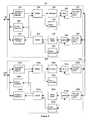
- FIG. 4depicts a preferred embodiment of bus arbiter and bridge circuit 28
- FIG. 5illustrates its operation.
- the originating processor in step S 21applies a bus access request signal on line 30 to bus access arbiter 122 .
- step S 22when the bus is available, arbiter 122 returns an access granted signal on line 30 ′, and so the requesting peripheral unit applies the message to bus 18 .
- a bus access request line 30 and an access granted line 30 ′are included in each line 30 a - 30 g of FIG. 1 .
- Bus access arbiter 122applies the address of the originating processor to access control table select circuit 120 .
- Access control tables 124include a look-up table for the address of each processor 20 , 22 , 24 , etc. Each look-up table lists the addresses of peripheral units throughout the entire system to which the processor at the corresponding originating address is permitted to communicate.
- Access control table select circuit 120selects the look-up table of the originating processor address, and the addresses to which the processor at that address is permitted to communicate are applied to comparison circuit 116 .
- step S 23determines the message destination address and applies it to comparison circuit 116 . If comparison circuit 116 determines in step S 24 that the message destination address is on the look-up table for the address of the originating processor, indicating that the processor at that originating address is permitted to communicate with the destination address, then comparison circuit 116 applies a signal to bus access arbiter 122 to indicate that the communication is authorized, freeing bus access arbiter 122 to await the next bus access request.
- step S 25destination address detector 110 also determines whether the destination address is on bus 18 within data processing unit 10 . If so, then in step S 26 the originating processor applies the message onto bus 18 to the destination processor and returns to step S 21 to await the next bus access request.
- comparison circuit 116determines that the message destination address is not on the look-up table for the originating processor address, then in step S 27 comparison circuit 116 generates an error signal or flag which is applied by bus 117 to maintenance processor 69 (FIG. 1) which then applies a signal on bus 119 to the processor at the originating address to prevent further transmissions from that address.
- gateway unit 16 or one of the processors 20 , 22 , 24 , etc. within data processing unit 10applies a message to bus 18 for a peripheral unit outside data processing unit 10
- the messageis applied by bus 18 to destination address detector 110 within bus arbiter and bridge circuit 28 , as well as to destination address detector 114 .
- the sideband signal indicating the sensitivity level of the originating addressis applied by bus 18 to sideband interface 118 .
- destination address detector 114applies the destination address to comparison circuit 116 .
- the sideband signal from interface 118is applied to access control table select circuit 120 , and this signal is given priority over the originating address indication from bus access arbiter 122 .
- Access control table select circuit 120selects the corresponding look-up table from access control tables 124 and applies it to comparison circuit 116 .
- comparison circuit 116determines whether the destination address is in the look-up table, indicating that the processor at the originating address is permitted to transmit messages to the destination address. If comparison circuit 116 determines that transmission of the message to the destination address is permitted, then comparison circuit 116 applies an enable signal to bridge control CPU 126 and clears bus access arbiter 122 to await the next bus access request.
- step S 25destination address detector 110 determines that the destination address is not on the bus 18 of data processing unit 10 , destination address detector 110 stores the message in buffer 112 and sideband interface 118 stores the sensitivity sideband signal in buffer 112 . If desired, destination address detectors 110 and 114 could be incorporated into a single address detector which then applies the message to buffer 112 and the destination address to comparison circuit 116 .
- step S 28bridge control CPU 126 receives the enable signal from comparison circuit 116 and, through output interface 128 , requests access to bus 129 . When that access is granted, then in step S 29 the bridge control CPU applies the message from buffer 112 through output interface 128 to output bus 129 and the sensitivity sideband signal from buffer 112 through sideband interface unit 130 to line 129 .
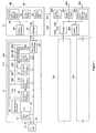
- control unit 12 aIf the message is for a unit connected to control unit 12 a (FIG. 1 ), then the message and the sensitivity sideband signal on bus 129 are applied to control unit 12 in which they are applied through bridge 32 to bus 35 which applies them to cross-rack interface unit 42 .
- Bridge circuit 32is also connected by bus 35 to other components within control unit 12 , such as a control processor 36 , a communication security control panel 38 , and an audio control panel 40 .
- Communication security panel 38is coupled by line 44 to communication equipment within the aircraft or other system.
- audio control panel 40is connected by line 46 to audio equipment within the aircraft or other system.
- Cross-rack interface unit 42 within control unit 12is connected by bus 154 to cross-rack interface unit 42 a within control unit 12 a .
- the corresponding components within data processing units 10 a , 10 b , etc.,are connected by bus 129 to the bridge circuit 32 a and control processor 36 a of control unit 12 a.
- FIG. 6is a block diagram of a preferred embodiment of cross-rack interface unit 42 and cross-rack interface unit 42 a , and FIG. 7 illustrates their operation.
- step S 41if a message and a sensitivity sideband signal are on bus 35 , the message is applied to destination address detector 140 , while the sensitivity sideband signal is applied to sideband interface unit 142 .
- Destination address detector 140detects the message destination address in step S 42 .
- the message, including the destination addressis applied by destination address detector 140 to buffer 144 .
- the sensitivity sideband signalis also applied to buffer 144 by sideband interface unit 142 .
- Buffer 144applies the message and destination address to serializer 146 , which in step S 43 converts the message and destination address into serial data.
- Buffer 144also applies the sensitivity sideband signal to token generator 148 , which in step S 44 converts the sensitivity sideband signal into a token.
- step S 45the serialized message and destination address and the token are applied from cross-rack interface unit 42 to cross-rack interface unit 42 a .
- the outputs of serializer 146 and token generator 148are applied to the two signal inputs of multiplexer 150 .
- Transmit control CPU 152applies a control signal to the control input of multiplexer 150 to properly multiplex the token with the serial data.
- the multiplexed token and serial data from multiplexer 150are applied by CPU 152 to cross-rack bus 154 from which they are applied to receive control CPU 156 a within cross-rack interface unit 42 a.
- the multiplexed signalincludes the destination address, the token, and the message.
- Receive control CPU 156 aapplies the multiplexed signal to the signal input of demultiplexer 158 a and applies a control signal to the control input of the demultiplexer.
- the destination address and messageare applied to deserializer 160 a
- the tokenis applied to token detector 162 a .
- deserializerconverts the serial data back into the message and destination address.
- token detector 162 aconverts the token into the sensitivity sideband signal.
- the outputs of deserializer 160 a and token detector 162 aare applied to buffer 164 a .
- Buffer 164 aapplies the destination address and the message to output interface unit 166 a which requests access to bus 35 , and when that access is granted in step S 48 applies the destination address and message to bus 35 a for application to bridge circuit 32 a within control unit 12 a .
- buffer 164 aapplies the sensitivity sideband signal to sideband interface unit 142 a which applies it on bus 35 a to bridge circuit 32 a within control unit 12 a . The process then returns to step S 41 to await the next message.
- Bridge circuit 32is similar to bridge circuit 28 , with bus 35 in place of bus 18 .
- Cross-rack interface unit 42is the originating address for signals passed from it to bridge circuit 32 . Since cross-rack interface unit 42 handles both sensitive and non-sensitive messages, the sensitivity level is indicated by the sideband signal.
- the message and sensitivity sideband signalare applied on bus 129 to the bus arbiter and bridge circuit within the data processing unit of the destination address for application to the destination bus in step S 29 (FIG. 5) and then application by that bus to the destination address.
- bridge circuit 32 in control unit 12applies a message and sensitivity sideband signal on bus 129 to bus arbiter and bridge circuit 28 in data processing unit 10
- the destination address and messageare applied to destination address detector 170 (FIG. 4) which determines that the message is for a peripheral component in data processing unit 10 , and so stores the destination address and message in buffer 172 .
- the sensitivity sideband signalis applied by bus 129 to sideband interface unit 130 which stores it in buffer 172 .
- Bus control CPU 126then requests access to bus 18 , and when bus access arbiter 122 gives that access, bridge control CPU 126 applies the destination address and message to output interface 174 which, in turn, applies them to bus 18 for communication to the destination address.
- bridge control CPU 126applies the sensitivity sideband signal through sideband interface 118 to bus 18 which then applies both the message and the sensitivity sideband signal to gateway unit 16 .
- the gateway unitthen reformats the message and passes the reformatted message to input/output unit 14 , as described above with reference to FIGS. 2 and 3. If the sensitivity level of the destination address is not confirmed by message formatting and sensitivity confirmation unit 66 , the unit can respond by not applying the message to buffer 72 , since maintenance processor 69 in data processing unit 10 cannot affect an originating processor outside unit 10 .
- a peripheral component in data processing unit 10 aoriginates a message for a peripheral component in data processing unit 10 b , so that the message does not need to go through control unit 12 a , the message, destination address, and sensitivity sideband signal are communicated directly from bus arbiter and bridge circuit 28 a in data processing unit 10 a to bus arbiter and bridge circuit 28 b in data processing unit 10 b.
- maintenance processor 69can prevent communication of further messages by causing the first peripheral component to shut down, by prohibiting bus access arbiter 122 from providing a further access request granted signal on line 30 ′, by preventing bridge control CPU 126 from applying further messages to output interface 174 or preventing the output interface from passing further messages, or by any other suitable technique.
- the present inventionprovides an improved, economical apparatus and method for controlling communication between peripheral components in a communication system.
Landscapes
- Engineering & Computer Science (AREA)
- Theoretical Computer Science (AREA)
- Computer Hardware Design (AREA)
- General Engineering & Computer Science (AREA)
- Physics & Mathematics (AREA)
- General Physics & Mathematics (AREA)
- Computer Security & Cryptography (AREA)
- Software Systems (AREA)
- Small-Scale Networks (AREA)
Abstract
Description
Claims (7)
Priority Applications (1)
| Application Number | Priority Date | Filing Date | Title |
|---|---|---|---|
| US09/481,331US6473825B1 (en) | 2000-01-12 | 2000-01-12 | Apparatus and method for controlling secure communications between peripheral components on computer buses connected by a bridge circuit |
Applications Claiming Priority (1)
| Application Number | Priority Date | Filing Date | Title |
|---|---|---|---|
| US09/481,331US6473825B1 (en) | 2000-01-12 | 2000-01-12 | Apparatus and method for controlling secure communications between peripheral components on computer buses connected by a bridge circuit |
Publications (1)
| Publication Number | Publication Date |
|---|---|
| US6473825B1true US6473825B1 (en) | 2002-10-29 |
Family
ID=23911539
Family Applications (1)
| Application Number | Title | Priority Date | Filing Date |
|---|---|---|---|
| US09/481,331Expired - LifetimeUS6473825B1 (en) | 2000-01-12 | 2000-01-12 | Apparatus and method for controlling secure communications between peripheral components on computer buses connected by a bridge circuit |
Country Status (1)
| Country | Link |
|---|---|
| US (1) | US6473825B1 (en) |
Cited By (40)
| Publication number | Priority date | Publication date | Assignee | Title |
|---|---|---|---|---|
| US20020138677A1 (en)* | 2001-03-26 | 2002-09-26 | International Business Machines Corporation | Selective targeting of transactions to devices on a shared bus |
| US20030172214A1 (en)* | 2002-03-08 | 2003-09-11 | Moyer William C. | Data processing system with peripheral access protection and method therefor |
| US20040111578A1 (en)* | 2002-09-05 | 2004-06-10 | Goodman Reginald A. | Personal computer internet security system |
| US20040236892A1 (en)* | 2003-03-04 | 2004-11-25 | Zhu De Sheng | Method, system and device for a processor to access devices of different speeds using a standard memory bus |
| US20040243823A1 (en)* | 2003-05-29 | 2004-12-02 | Moyer William C. | Method and apparatus for determining access permission |
| US20060005098A1 (en)* | 2004-06-30 | 2006-01-05 | Marcus Lotz | Interface workbench for high volume data buffering and connectivity |
| US20060059302A1 (en)* | 2004-09-14 | 2006-03-16 | Susumu Tsuruta | Disk array subsystem |
| US20080259998A1 (en)* | 2007-04-17 | 2008-10-23 | Cypress Semiconductor Corp. | Temperature sensor with digital bandgap |
| US20080294806A1 (en)* | 2007-04-17 | 2008-11-27 | Cypress Semiconductor Corporation | Programmable system-on-chip hub |
| US20080297388A1 (en)* | 2007-04-17 | 2008-12-04 | Cypress Semiconductor Corporation | Programmable sigma-delta analog-to-digital converter |
| US20090066427A1 (en)* | 2005-02-04 | 2009-03-12 | Aaron Brennan | Poly-phase frequency synthesis oscillator |
| US20090144332A1 (en)* | 2007-11-29 | 2009-06-04 | Wallace Paul Montgomery | Sideband access based method and apparatus for determining software integrity |
| US20090144472A1 (en)* | 2007-11-29 | 2009-06-04 | Wallace Paul Montgomery | Method and apparatus for making a processor sideband interface adhere to secure mode restrictions |
| US20090184574A1 (en)* | 2008-01-17 | 2009-07-23 | Zavidniak Martin P | Communication System and Method Employing Line Replaceable Equipment Racks on an Aircraft |
| US7825688B1 (en) | 2000-10-26 | 2010-11-02 | Cypress Semiconductor Corporation | Programmable microcontroller architecture(mixed analog/digital) |
| US7844437B1 (en) | 2001-11-19 | 2010-11-30 | Cypress Semiconductor Corporation | System and method for performing next placements and pruning of disallowed placements for programming an integrated circuit |
| US7893724B2 (en) | 2004-03-25 | 2011-02-22 | Cypress Semiconductor Corporation | Method and circuit for rapid alignment of signals |
| US8026739B2 (en) | 2007-04-17 | 2011-09-27 | Cypress Semiconductor Corporation | System level interconnect with programmable switching |
| US8049569B1 (en) | 2007-09-05 | 2011-11-01 | Cypress Semiconductor Corporation | Circuit and method for improving the accuracy of a crystal-less oscillator having dual-frequency modes |
| US8067948B2 (en) | 2006-03-27 | 2011-11-29 | Cypress Semiconductor Corporation | Input/output multiplexer bus |
| US8069428B1 (en) | 2001-10-24 | 2011-11-29 | Cypress Semiconductor Corporation | Techniques for generating microcontroller configuration information |
| US8078970B1 (en) | 2001-11-09 | 2011-12-13 | Cypress Semiconductor Corporation | Graphical user interface with user-selectable list-box |
| US8078894B1 (en) | 2007-04-25 | 2011-12-13 | Cypress Semiconductor Corporation | Power management architecture, method and configuration system |
| US8085067B1 (en) | 2005-12-21 | 2011-12-27 | Cypress Semiconductor Corporation | Differential-to-single ended signal converter circuit and method |
| US8103496B1 (en) | 2000-10-26 | 2012-01-24 | Cypress Semicondutor Corporation | Breakpoint control in an in-circuit emulation system |
| US8103497B1 (en) | 2002-03-28 | 2012-01-24 | Cypress Semiconductor Corporation | External interface for event architecture |
| US8120408B1 (en) | 2005-05-05 | 2012-02-21 | Cypress Semiconductor Corporation | Voltage controlled oscillator delay cell and method |
| US8130025B2 (en) | 2007-04-17 | 2012-03-06 | Cypress Semiconductor Corporation | Numerical band gap |
| US8149048B1 (en) | 2000-10-26 | 2012-04-03 | Cypress Semiconductor Corporation | Apparatus and method for programmable power management in a programmable analog circuit block |
| US8160864B1 (en) | 2000-10-26 | 2012-04-17 | Cypress Semiconductor Corporation | In-circuit emulator and pod synchronized boot |
| US8176296B2 (en) | 2000-10-26 | 2012-05-08 | Cypress Semiconductor Corporation | Programmable microcontroller architecture |
| US20130047230A1 (en)* | 2011-08-17 | 2013-02-21 | International Business Machines Corporation | Building data security in a networked computing environment |
| US8402313B1 (en) | 2002-05-01 | 2013-03-19 | Cypress Semiconductor Corporation | Reconfigurable testing system and method |
| US8499270B1 (en) | 2007-04-25 | 2013-07-30 | Cypress Semiconductor Corporation | Configuration of programmable IC design elements |
| US8527949B1 (en) | 2001-11-19 | 2013-09-03 | Cypress Semiconductor Corporation | Graphical user interface for dynamically reconfiguring a programmable device |
| US9018979B2 (en) | 2007-04-17 | 2015-04-28 | Cypress Semiconductor Corporation | Universal digital block interconnection and channel routing |
| US9448964B2 (en) | 2009-05-04 | 2016-09-20 | Cypress Semiconductor Corporation | Autonomous control in a programmable system |
| US9720805B1 (en) | 2007-04-25 | 2017-08-01 | Cypress Semiconductor Corporation | System and method for controlling a target device |
| US10218614B2 (en)* | 2016-08-25 | 2019-02-26 | Honeywell International Inc. | Ethernet to spacewire bridge |
| US10698662B2 (en) | 2001-11-15 | 2020-06-30 | Cypress Semiconductor Corporation | System providing automatic source code generation for personalization and parameterization of user modules |
Citations (3)
| Publication number | Priority date | Publication date | Assignee | Title |
|---|---|---|---|---|
| US4540850A (en)* | 1983-04-29 | 1985-09-10 | At&T Bell Laboratories | Method and apparatus for controlling a conference |
| US5335266A (en)* | 1990-10-01 | 1994-08-02 | United States Advance Network, Inc. | Automated telecommunication peripheral system |
| US5809262A (en)* | 1995-05-17 | 1998-09-15 | Dell U.S.A., L.P. | Commonly housed multiple processor type computing system and method of manufacturing the same |
- 2000
- 2000-01-12USUS09/481,331patent/US6473825B1/ennot_activeExpired - Lifetime
Patent Citations (3)
| Publication number | Priority date | Publication date | Assignee | Title |
|---|---|---|---|---|
| US4540850A (en)* | 1983-04-29 | 1985-09-10 | At&T Bell Laboratories | Method and apparatus for controlling a conference |
| US5335266A (en)* | 1990-10-01 | 1994-08-02 | United States Advance Network, Inc. | Automated telecommunication peripheral system |
| US5809262A (en)* | 1995-05-17 | 1998-09-15 | Dell U.S.A., L.P. | Commonly housed multiple processor type computing system and method of manufacturing the same |
Cited By (74)
| Publication number | Priority date | Publication date | Assignee | Title |
|---|---|---|---|---|
| US8103496B1 (en) | 2000-10-26 | 2012-01-24 | Cypress Semicondutor Corporation | Breakpoint control in an in-circuit emulation system |
| US10020810B2 (en) | 2000-10-26 | 2018-07-10 | Cypress Semiconductor Corporation | PSoC architecture |
| US9843327B1 (en) | 2000-10-26 | 2017-12-12 | Cypress Semiconductor Corporation | PSOC architecture |
| US8555032B2 (en) | 2000-10-26 | 2013-10-08 | Cypress Semiconductor Corporation | Microcontroller programmable system on a chip with programmable interconnect |
| US10261932B2 (en) | 2000-10-26 | 2019-04-16 | Cypress Semiconductor Corporation | Microcontroller programmable system on a chip |
| US8736303B2 (en) | 2000-10-26 | 2014-05-27 | Cypress Semiconductor Corporation | PSOC architecture |
| US8149048B1 (en) | 2000-10-26 | 2012-04-03 | Cypress Semiconductor Corporation | Apparatus and method for programmable power management in a programmable analog circuit block |
| US8358150B1 (en) | 2000-10-26 | 2013-01-22 | Cypress Semiconductor Corporation | Programmable microcontroller architecture(mixed analog/digital) |
| US8160864B1 (en) | 2000-10-26 | 2012-04-17 | Cypress Semiconductor Corporation | In-circuit emulator and pod synchronized boot |
| US7825688B1 (en) | 2000-10-26 | 2010-11-02 | Cypress Semiconductor Corporation | Programmable microcontroller architecture(mixed analog/digital) |
| US8176296B2 (en) | 2000-10-26 | 2012-05-08 | Cypress Semiconductor Corporation | Programmable microcontroller architecture |
| US10725954B2 (en) | 2000-10-26 | 2020-07-28 | Monterey Research, Llc | Microcontroller programmable system on a chip |
| US10248604B2 (en) | 2000-10-26 | 2019-04-02 | Cypress Semiconductor Corporation | Microcontroller programmable system on a chip |
| US9766650B2 (en) | 2000-10-26 | 2017-09-19 | Cypress Semiconductor Corporation | Microcontroller programmable system on a chip with programmable interconnect |
| US20020138677A1 (en)* | 2001-03-26 | 2002-09-26 | International Business Machines Corporation | Selective targeting of transactions to devices on a shared bus |
| US6662251B2 (en)* | 2001-03-26 | 2003-12-09 | International Business Machines Corporation | Selective targeting of transactions to devices on a shared bus |
| US8793635B1 (en) | 2001-10-24 | 2014-07-29 | Cypress Semiconductor Corporation | Techniques for generating microcontroller configuration information |
| US10466980B2 (en) | 2001-10-24 | 2019-11-05 | Cypress Semiconductor Corporation | Techniques for generating microcontroller configuration information |
| US8069428B1 (en) | 2001-10-24 | 2011-11-29 | Cypress Semiconductor Corporation | Techniques for generating microcontroller configuration information |
| US8078970B1 (en) | 2001-11-09 | 2011-12-13 | Cypress Semiconductor Corporation | Graphical user interface with user-selectable list-box |
| US10698662B2 (en) | 2001-11-15 | 2020-06-30 | Cypress Semiconductor Corporation | System providing automatic source code generation for personalization and parameterization of user modules |
| US8527949B1 (en) | 2001-11-19 | 2013-09-03 | Cypress Semiconductor Corporation | Graphical user interface for dynamically reconfiguring a programmable device |
| US7844437B1 (en) | 2001-11-19 | 2010-11-30 | Cypress Semiconductor Corporation | System and method for performing next placements and pruning of disallowed placements for programming an integrated circuit |
| US8370791B2 (en) | 2001-11-19 | 2013-02-05 | Cypress Semiconductor Corporation | System and method for performing next placements and pruning of disallowed placements for programming an integrated circuit |
| US8533677B1 (en) | 2001-11-19 | 2013-09-10 | Cypress Semiconductor Corporation | Graphical user interface for dynamically reconfiguring a programmable device |
| US20030172214A1 (en)* | 2002-03-08 | 2003-09-11 | Moyer William C. | Data processing system with peripheral access protection and method therefor |
| US7277972B2 (en)* | 2002-03-08 | 2007-10-02 | Freescale Semiconductor, Inc. | Data processing system with peripheral access protection and method therefor |
| US8103497B1 (en) | 2002-03-28 | 2012-01-24 | Cypress Semiconductor Corporation | External interface for event architecture |
| US8402313B1 (en) | 2002-05-01 | 2013-03-19 | Cypress Semiconductor Corporation | Reconfigurable testing system and method |
| US7146640B2 (en) | 2002-09-05 | 2006-12-05 | Exobox Technologies Corp. | Personal computer internet security system |
| US20040111578A1 (en)* | 2002-09-05 | 2004-06-10 | Goodman Reginald A. | Personal computer internet security system |
| US7103691B2 (en)* | 2003-03-04 | 2006-09-05 | Hewlett-Packard Development Company, L.P. | Method, system and device for a processor to access devices of different speeds using a standard memory bus |
| US20040236892A1 (en)* | 2003-03-04 | 2004-11-25 | Zhu De Sheng | Method, system and device for a processor to access devices of different speeds using a standard memory bus |
| US7444668B2 (en)* | 2003-05-29 | 2008-10-28 | Freescale Semiconductor, Inc. | Method and apparatus for determining access permission |
| US20040243823A1 (en)* | 2003-05-29 | 2004-12-02 | Moyer William C. | Method and apparatus for determining access permission |
| US7893724B2 (en) | 2004-03-25 | 2011-02-22 | Cypress Semiconductor Corporation | Method and circuit for rapid alignment of signals |
| US7487427B2 (en)* | 2004-06-30 | 2009-02-03 | Sap Ag | Interface workbench for high volume data buffering and connectivity |
| US20060005098A1 (en)* | 2004-06-30 | 2006-01-05 | Marcus Lotz | Interface workbench for high volume data buffering and connectivity |
| US20060059302A1 (en)* | 2004-09-14 | 2006-03-16 | Susumu Tsuruta | Disk array subsystem |
| US8085100B2 (en) | 2005-02-04 | 2011-12-27 | Cypress Semiconductor Corporation | Poly-phase frequency synthesis oscillator |
| US20090066427A1 (en)* | 2005-02-04 | 2009-03-12 | Aaron Brennan | Poly-phase frequency synthesis oscillator |
| US8120408B1 (en) | 2005-05-05 | 2012-02-21 | Cypress Semiconductor Corporation | Voltage controlled oscillator delay cell and method |
| US8085067B1 (en) | 2005-12-21 | 2011-12-27 | Cypress Semiconductor Corporation | Differential-to-single ended signal converter circuit and method |
| US8717042B1 (en) | 2006-03-27 | 2014-05-06 | Cypress Semiconductor Corporation | Input/output multiplexer bus |
| US8067948B2 (en) | 2006-03-27 | 2011-11-29 | Cypress Semiconductor Corporation | Input/output multiplexer bus |
| US8130025B2 (en) | 2007-04-17 | 2012-03-06 | Cypress Semiconductor Corporation | Numerical band gap |
| US8092083B2 (en) | 2007-04-17 | 2012-01-10 | Cypress Semiconductor Corporation | Temperature sensor with digital bandgap |
| US10826499B2 (en) | 2007-04-17 | 2020-11-03 | Cypress Semiconductor Corporation | System level interconnect with programmable switching |
| US20080259998A1 (en)* | 2007-04-17 | 2008-10-23 | Cypress Semiconductor Corp. | Temperature sensor with digital bandgap |
| US20080294806A1 (en)* | 2007-04-17 | 2008-11-27 | Cypress Semiconductor Corporation | Programmable system-on-chip hub |
| US10516397B2 (en) | 2007-04-17 | 2019-12-24 | Cypress Semiconductor Corporation | System level interconnect with programmable switching |
| US8572297B2 (en)* | 2007-04-17 | 2013-10-29 | Cypress Semiconductor Corporation | Programmable system-on-chip hub |
| US9553588B2 (en) | 2007-04-17 | 2017-01-24 | Cypress Semiconductor Corporation | System level interconnect with programmable switching |
| US8476928B1 (en) | 2007-04-17 | 2013-07-02 | Cypress Semiconductor Corporation | System level interconnect with programmable switching |
| US20080297388A1 (en)* | 2007-04-17 | 2008-12-04 | Cypress Semiconductor Corporation | Programmable sigma-delta analog-to-digital converter |
| US10097185B2 (en) | 2007-04-17 | 2018-10-09 | Cypress Semiconductor Corporation | System level interconnect with programmable switching |
| US8026739B2 (en) | 2007-04-17 | 2011-09-27 | Cypress Semiconductor Corporation | System level interconnect with programmable switching |
| US9018979B2 (en) | 2007-04-17 | 2015-04-28 | Cypress Semiconductor Corporation | Universal digital block interconnection and channel routing |
| US9325320B1 (en) | 2007-04-17 | 2016-04-26 | Cypress Semiconductor Corporation | System level interconnect with programmable switching |
| US8040266B2 (en) | 2007-04-17 | 2011-10-18 | Cypress Semiconductor Corporation | Programmable sigma-delta analog-to-digital converter |
| US8078894B1 (en) | 2007-04-25 | 2011-12-13 | Cypress Semiconductor Corporation | Power management architecture, method and configuration system |
| US8499270B1 (en) | 2007-04-25 | 2013-07-30 | Cypress Semiconductor Corporation | Configuration of programmable IC design elements |
| US8909960B1 (en) | 2007-04-25 | 2014-12-09 | Cypress Semiconductor Corporation | Power management architecture, method and configuration system |
| US9720805B1 (en) | 2007-04-25 | 2017-08-01 | Cypress Semiconductor Corporation | System and method for controlling a target device |
| US8049569B1 (en) | 2007-09-05 | 2011-11-01 | Cypress Semiconductor Corporation | Circuit and method for improving the accuracy of a crystal-less oscillator having dual-frequency modes |
| US20090144332A1 (en)* | 2007-11-29 | 2009-06-04 | Wallace Paul Montgomery | Sideband access based method and apparatus for determining software integrity |
| US8250354B2 (en)* | 2007-11-29 | 2012-08-21 | GlobalFoundries, Inc. | Method and apparatus for making a processor sideband interface adhere to secure mode restrictions |
| US20090144472A1 (en)* | 2007-11-29 | 2009-06-04 | Wallace Paul Montgomery | Method and apparatus for making a processor sideband interface adhere to secure mode restrictions |
| US20090184574A1 (en)* | 2008-01-17 | 2009-07-23 | Zavidniak Martin P | Communication System and Method Employing Line Replaceable Equipment Racks on an Aircraft |
| US8120894B2 (en)* | 2008-01-17 | 2012-02-21 | Northrop Grumman Systems Corporation | Communication system and method employing line replaceable equipment racks on an aircraft |
| US9448964B2 (en) | 2009-05-04 | 2016-09-20 | Cypress Semiconductor Corporation | Autonomous control in a programmable system |
| US8782762B2 (en)* | 2011-08-17 | 2014-07-15 | International Business Machines Corporation | Building data security in a networked computing environment |
| US20130047230A1 (en)* | 2011-08-17 | 2013-02-21 | International Business Machines Corporation | Building data security in a networked computing environment |
| US10218614B2 (en)* | 2016-08-25 | 2019-02-26 | Honeywell International Inc. | Ethernet to spacewire bridge |
Similar Documents
| Publication | Publication Date | Title |
|---|---|---|
| US6473825B1 (en) | Apparatus and method for controlling secure communications between peripheral components on computer buses connected by a bridge circuit | |
| US6289105B1 (en) | Method and apparatus for encrypting and transferring electronic mails | |
| US5386471A (en) | Method and apparatus for securely conveying network control data across a cryptographic boundary | |
| US5818939A (en) | Optimized security functionality in an electronic system | |
| US10284553B2 (en) | Relay apparatus, terminal apparatus, and communication method | |
| US6389533B1 (en) | Anonymity server | |
| US6643698B2 (en) | Mixed enclave operation in a computer network | |
| US8478997B2 (en) | Multi-level security software architecture | |
| US7624180B2 (en) | Mixed enclave operation in a computer network | |
| US5828832A (en) | Mixed enclave operation in a computer network with multi-level network security | |
| EP0711051B1 (en) | Data processing system with verification of authenticity of cryptographic algorithms according to the challenge/response principle | |
| KR100414238B1 (en) | Secure network protocol system and method | |
| US11436873B2 (en) | Encrypted communication system and method for controlling encrypted communication system | |
| JP2661793B2 (en) | Distributed information system with automatic invocation of key management negotiation protocol | |
| EP0082958A2 (en) | Cryptographic data communications | |
| US8401000B2 (en) | Method of processing data packets | |
| US20030233409A1 (en) | Electronic mail distribution network implementation for safeguarding sender's address book covering addressee aliases with minimum interference with normal electronic mail transmission | |
| JP2006523347A (en) | Data processing system and method having peripheral device access protection | |
| US6272639B1 (en) | Mixed enclave operation in a computer network | |
| CN114826733B (en) | File transmission method, device, system, equipment, medium and program product | |
| NO311909B1 (en) | Procedure for protected distribution protocol for key and certificate material | |
| US20190305939A1 (en) | Vehicle communication system and vehicle communication method | |
| US7607167B1 (en) | Secure gateway/router | |
| WO2021262251A1 (en) | Shared resource identification | |
| US20070070904A1 (en) | Feedback mechanism for flexible load balancing in a flow-based processor affinity scheme |
Legal Events
| Date | Code | Title | Description |
|---|---|---|---|
| AS | Assignment | Owner name:TRW INC., CALIFORNIA Free format text:ASSIGNMENT OF ASSIGNORS INTEREST;ASSIGNORS:WORLEY, JAMES F.;BLASDEL, MICHAEL J.;HALE, ROBERT R.;AND OTHERS;REEL/FRAME:010700/0575 Effective date:20000118 | |
| STCF | Information on status: patent grant | Free format text:PATENTED CASE | |
| AS | Assignment | Owner name:NORTHROP GRUMMAN CORPORATION, CALIFORNIA Free format text:ASSIGNMENT OF ASSIGNORS INTEREST;ASSIGNOR:TRW, INC. N/K/A NORTHROP GRUMMAN SPACE AND MISSION SYSTEMS CORPORATION, AN OHIO CORPORATION;REEL/FRAME:013751/0849 Effective date:20030122 Owner name:NORTHROP GRUMMAN CORPORATION,CALIFORNIA Free format text:ASSIGNMENT OF ASSIGNORS INTEREST;ASSIGNOR:TRW, INC. N/K/A NORTHROP GRUMMAN SPACE AND MISSION SYSTEMS CORPORATION, AN OHIO CORPORATION;REEL/FRAME:013751/0849 Effective date:20030122 | |
| FPAY | Fee payment | Year of fee payment:4 | |
| FEPP | Fee payment procedure | Free format text:PAYOR NUMBER ASSIGNED (ORIGINAL EVENT CODE: ASPN); ENTITY STATUS OF PATENT OWNER: LARGE ENTITY | |
| AS | Assignment | Owner name:NORTHROP GRUMMAN SPACE & MISSION SYSTEMS CORP.,CAL Free format text:ASSIGNMENT OF ASSIGNORS INTEREST;ASSIGNOR:NORTHROP GRUMMAN CORPORTION;REEL/FRAME:023699/0551 Effective date:20091125 Owner name:NORTHROP GRUMMAN SPACE & MISSION SYSTEMS CORP., CA Free format text:ASSIGNMENT OF ASSIGNORS INTEREST;ASSIGNOR:NORTHROP GRUMMAN CORPORTION;REEL/FRAME:023699/0551 Effective date:20091125 | |
| AS | Assignment | Owner name:NORTHROP GRUMMAN SYSTEMS CORPORATION,CALIFORNIA Free format text:ASSIGNMENT OF ASSIGNORS INTEREST;ASSIGNOR:NORTHROP GRUMMAN SPACE & MISSION SYSTEMS CORP.;REEL/FRAME:023915/0446 Effective date:20091210 Owner name:NORTHROP GRUMMAN SYSTEMS CORPORATION, CALIFORNIA Free format text:ASSIGNMENT OF ASSIGNORS INTEREST;ASSIGNOR:NORTHROP GRUMMAN SPACE & MISSION SYSTEMS CORP.;REEL/FRAME:023915/0446 Effective date:20091210 | |
| FPAY | Fee payment | Year of fee payment:8 | |
| FPAY | Fee payment | Year of fee payment:12 |