US6473072B1 - Microencapsulated electrophoretic electrostatically-addressed media for drawing device applications - Google Patents
Microencapsulated electrophoretic electrostatically-addressed media for drawing device applicationsDownload PDFInfo
- Publication number
- US6473072B1 US6473072B1US09/310,300US31030099AUS6473072B1US 6473072 B1US6473072 B1US 6473072B1US 31030099 AUS31030099 AUS 31030099AUS 6473072 B1US6473072 B1US 6473072B1
- Authority
- US
- United States
- Prior art keywords
- display
- media
- display media
- electrode
- sliding bar
- Prior art date
- Legal status (The legal status is an assumption and is not a legal conclusion. Google has not performed a legal analysis and makes no representation as to the accuracy of the status listed.)
- Expired - Lifetime
Links
- 239000002245particleSubstances0.000claimsabstractdescription49
- 239000002775capsuleSubstances0.000claimsabstractdescription36
- 230000005684electric fieldEffects0.000claimsabstractdescription31
- 239000012530fluidSubstances0.000claimsabstractdescription13
- 241001422033ThestylusSpecies0.000claimsdescription43
- 230000007246mechanismEffects0.000claimsdescription23
- 238000000034methodMethods0.000claimsdescription23
- 239000004020conductorSubstances0.000claimsdescription22
- 239000010410layerSubstances0.000claimsdescription22
- 239000000758substrateSubstances0.000claimsdescription22
- 239000011241protective layerSubstances0.000claimsdescription21
- 239000011230binding agentSubstances0.000claimsdescription15
- 229920000642polymerPolymers0.000claimsdescription14
- 238000000576coating methodMethods0.000claimsdescription12
- 239000011248coating agentSubstances0.000claimsdescription10
- 238000004891communicationMethods0.000claimsdescription7
- 238000013500data storageMethods0.000claimsdescription6
- 239000012190activatorSubstances0.000claimsdescription5
- 238000003860storageMethods0.000claimsdescription5
- 230000004913activationEffects0.000claimsdescription4
- 239000003086colorantSubstances0.000claimsdescription4
- 230000001681protective effectEffects0.000claimsdescription3
- 239000013536elastomeric materialSubstances0.000claimsdescription2
- 238000005096rolling processMethods0.000claimsdescription2
- FGUUSXIOTUKUDN-IBGZPJMESA-NC1(=CC=CC=C1)N1C2=C(NC([C@H](C1)NC=1OC(=NN=1)C1=CC=CC=C1)=O)C=CC=C2Chemical compoundC1(=CC=CC=C1)N1C2=C(NC([C@H](C1)NC=1OC(=NN=1)C1=CC=CC=C1)=O)C=CC=C2FGUUSXIOTUKUDN-IBGZPJMESA-N0.000claims1
- 239000000976inkSubstances0.000description22
- 239000000463materialSubstances0.000description21
- 230000003287optical effectEffects0.000description9
- 239000011347resinSubstances0.000description9
- 229920005989resinPolymers0.000description9
- XLYOFNOQVPJJNP-UHFFFAOYSA-NwaterSubstancesOXLYOFNOQVPJJNP-UHFFFAOYSA-N0.000description9
- 238000007639printingMethods0.000description8
- 239000002904solventSubstances0.000description8
- 239000003990capacitorSubstances0.000description7
- 230000008859changeEffects0.000description7
- 239000000203mixtureSubstances0.000description7
- 239000004973liquid crystal related substanceSubstances0.000description6
- -1polyphenylenevinylenePolymers0.000description6
- 239000004417polycarbonateSubstances0.000description5
- 229920000515polycarbonatePolymers0.000description5
- GWEVSGVZZGPLCZ-UHFFFAOYSA-NTitan oxideChemical compoundO=[Ti]=OGWEVSGVZZGPLCZ-UHFFFAOYSA-N0.000description4
- 230000008901benefitEffects0.000description4
- 239000006185dispersionSubstances0.000description4
- 230000000694effectsEffects0.000description4
- 238000004519manufacturing processMethods0.000description4
- 239000000178monomerSubstances0.000description4
- 230000006870functionEffects0.000description3
- 239000003550markerSubstances0.000description3
- 229920003023plasticPolymers0.000description3
- 239000004033plasticSubstances0.000description3
- 229920000728polyesterPolymers0.000description3
- 230000008569processEffects0.000description3
- 239000011253protective coatingSubstances0.000description3
- 230000005855radiationEffects0.000description3
- 239000007787solidSubstances0.000description3
- 230000003068static effectEffects0.000description3
- 239000000725suspensionSubstances0.000description3
- 229920001169thermoplasticPolymers0.000description3
- 238000012546transferMethods0.000description3
- BQCIDUSAKPWEOX-UHFFFAOYSA-N1,1-DifluoroetheneChemical compoundFC(F)=CBQCIDUSAKPWEOX-UHFFFAOYSA-N0.000description2
- 239000004593EpoxySubstances0.000description2
- 229920004142LEXAN™Polymers0.000description2
- 239000004418LexanSubstances0.000description2
- 239000000853adhesiveSubstances0.000description2
- 230000001070adhesive effectEffects0.000description2
- 229920001940conductive polymerPolymers0.000description2
- 239000002872contrast mediaSubstances0.000description2
- 229940039231contrast mediaDrugs0.000description2
- 239000012769display materialSubstances0.000description2
- 150000004676glycansChemical class0.000description2
- AMGQUBHHOARCQH-UHFFFAOYSA-Nindium;oxotinChemical compound[In].[Sn]=OAMGQUBHHOARCQH-UHFFFAOYSA-N0.000description2
- 229920000126latexPolymers0.000description2
- 239000011159matrix materialSubstances0.000description2
- 230000005012migrationEffects0.000description2
- 238000013508migrationMethods0.000description2
- 230000036961partial effectEffects0.000description2
- 239000000049pigmentSubstances0.000description2
- 229920000553poly(phenylenevinylene)Polymers0.000description2
- 229920000767polyanilinePolymers0.000description2
- 229920001282polysaccharidePolymers0.000description2
- 239000005017polysaccharideSubstances0.000description2
- 229920000123polythiophenePolymers0.000description2
- 229920002635polyurethanePolymers0.000description2
- 239000004814polyurethaneSubstances0.000description2
- 229920002620polyvinyl fluoridePolymers0.000description2
- 238000003825pressingMethods0.000description2
- 239000001044red dyeSubstances0.000description2
- 230000004044responseEffects0.000description2
- 238000000926separation methodMethods0.000description2
- 241000894007speciesSpecies0.000description2
- 229920001187thermosetting polymerPolymers0.000description2
- 229920003169water-soluble polymerPolymers0.000description2
- 2299400950952-hydroxyethyl acrylateDrugs0.000description1
- OMIGHNLMNHATMP-UHFFFAOYSA-N2-hydroxyethyl prop-2-enoateChemical compoundOCCOC(=O)C=COMIGHNLMNHATMP-UHFFFAOYSA-N0.000description1
- NOWKCMXCCJGMRR-UHFFFAOYSA-NAziridineChemical compoundC1CN1NOWKCMXCCJGMRR-UHFFFAOYSA-N0.000description1
- 229920002799BoPETPolymers0.000description1
- OKTJSMMVPCPJKN-UHFFFAOYSA-NCarbonChemical compound[C]OKTJSMMVPCPJKN-UHFFFAOYSA-N0.000description1
- 239000004971Cross linkerSubstances0.000description1
- CWYNVVGOOAEACU-UHFFFAOYSA-NFe2+Chemical compound[Fe+2]CWYNVVGOOAEACU-UHFFFAOYSA-N0.000description1
- MHAJPDPJQMAIIY-UHFFFAOYSA-NHydrogen peroxideChemical compoundOOMHAJPDPJQMAIIY-UHFFFAOYSA-N0.000description1
- 239000005041Mylar™Substances0.000description1
- SECXISVLQFMRJM-UHFFFAOYSA-NN-MethylpyrrolidoneChemical compoundCN1CCCC1=OSECXISVLQFMRJM-UHFFFAOYSA-N0.000description1
- 239000004677NylonSubstances0.000description1
- 239000004698PolyethyleneSubstances0.000description1
- 241000083879Polyommatus icarusSpecies0.000description1
- 239000004743PolypropyleneSubstances0.000description1
- 229920002125Sokalan®Polymers0.000description1
- NIXOWILDQLNWCW-UHFFFAOYSA-Nacrylic acid groupChemical groupC(C=C)(=O)ONIXOWILDQLNWCW-UHFFFAOYSA-N0.000description1
- 229920006397acrylic thermoplasticPolymers0.000description1
- 239000011149active materialSubstances0.000description1
- 238000005054agglomerationMethods0.000description1
- 230000002776aggregationEffects0.000description1
- HSFWRNGVRCDJHI-UHFFFAOYSA-Nalpha-acetyleneNatural productsC#CHSFWRNGVRCDJHI-UHFFFAOYSA-N0.000description1
- 238000013475authorizationMethods0.000description1
- WPYMKLBDIGXBTP-UHFFFAOYSA-Nbenzoic acidChemical compoundOC(=O)C1=CC=CC=C1WPYMKLBDIGXBTP-UHFFFAOYSA-N0.000description1
- QRUDEWIWKLJBPS-UHFFFAOYSA-NbenzotriazoleChemical compoundC1=CC=C2N[N][N]C2=C1QRUDEWIWKLJBPS-UHFFFAOYSA-N0.000description1
- 239000012964benzotriazoleSubstances0.000description1
- 125000003354benzotriazolyl groupChemical classN1N=NC2=C1C=CC=C2*0.000description1
- 229910002056binary alloyInorganic materials0.000description1
- 230000000740bleeding effectEffects0.000description1
- 239000001045blue dyeSubstances0.000description1
- 125000003178carboxy groupChemical group[H]OC(*)=O0.000description1
- 238000005119centrifugationMethods0.000description1
- 239000000084colloidal systemSubstances0.000description1
- 238000004040coloringMethods0.000description1
- 230000001010compromised effectEffects0.000description1
- 238000010276constructionMethods0.000description1
- 238000001816coolingMethods0.000description1
- 229920001577copolymerPolymers0.000description1
- 229920006037cross link polymerPolymers0.000description1
- 239000003431cross linking reagentSubstances0.000description1
- 238000013016dampingMethods0.000description1
- 238000013481data captureMethods0.000description1
- 238000013461designMethods0.000description1
- 238000010586diagramMethods0.000description1
- 239000003085diluting agentSubstances0.000description1
- 239000004815dispersion polymerSubstances0.000description1
- 238000006073displacement reactionMethods0.000description1
- 239000007772electrode materialSubstances0.000description1
- 238000005538encapsulationMethods0.000description1
- 125000003700epoxy groupChemical group0.000description1
- 239000004744fabricSubstances0.000description1
- 230000002349favourable effectEffects0.000description1
- 230000005669field effectEffects0.000description1
- 238000009472formulationMethods0.000description1
- 230000009477glass transitionEffects0.000description1
- 239000003292glueSubstances0.000description1
- 229910002804graphiteInorganic materials0.000description1
- 239000010439graphiteSubstances0.000description1
- 239000004519greaseSubstances0.000description1
- 239000001046green dyeSubstances0.000description1
- 229920001519homopolymerPolymers0.000description1
- 239000012943hotmeltSubstances0.000description1
- 230000002452interceptive effectEffects0.000description1
- 229920000554ionomerPolymers0.000description1
- 238000010030laminatingMethods0.000description1
- 239000004816latexSubstances0.000description1
- 239000004611light stabiliserSubstances0.000description1
- 230000000670limiting effectEffects0.000description1
- 229910052751metalInorganic materials0.000description1
- 239000002184metalSubstances0.000description1
- 229910044991metal oxideInorganic materials0.000description1
- 150000004706metal oxidesChemical class0.000description1
- 239000003094microcapsuleSubstances0.000description1
- 230000037230mobilityEffects0.000description1
- 150000002790naphthalenesChemical class0.000description1
- 229920001778nylonPolymers0.000description1
- 238000004806packaging method and processMethods0.000description1
- SLIUAWYAILUBJU-UHFFFAOYSA-NpentaceneChemical compoundC1=CC=CC2=CC3=CC4=CC5=CC=CC=C5C=C4C=C3C=C21SLIUAWYAILUBJU-UHFFFAOYSA-N0.000description1
- 230000035699permeabilityEffects0.000description1
- 230000002085persistent effectEffects0.000description1
- OJMIONKXNSYLSR-UHFFFAOYSA-Nphosphorous acidChemical compoundOP(O)OOJMIONKXNSYLSR-UHFFFAOYSA-N0.000description1
- IEQIEDJGQAUEQZ-UHFFFAOYSA-NphthalocyanineChemical compoundN1C(N=C2C3=CC=CC=C3C(N=C3C4=CC=CC=C4C(=N4)N3)=N2)=C(C=CC=C2)C2=C1N=C1C2=CC=CC=C2C4=N1IEQIEDJGQAUEQZ-UHFFFAOYSA-N0.000description1
- 229920003207poly(ethylene-2,6-naphthalate)Polymers0.000description1
- 229920003229poly(methyl methacrylate)Polymers0.000description1
- 229920002492poly(sulfone)Polymers0.000description1
- 229920001197polyacetylenePolymers0.000description1
- 229920000647polyepoxidePolymers0.000description1
- 229920000573polyethylenePolymers0.000description1
- 229920001223polyethylene glycolPolymers0.000description1
- 239000011112polyethylene naphthalateSubstances0.000description1
- 229920006254polymer filmPolymers0.000description1
- 239000002861polymer materialSubstances0.000description1
- 239000002952polymeric resinSubstances0.000description1
- 229920001155polypropylenePolymers0.000description1
- 229920000128polypyrrolePolymers0.000description1
- 229920001296polysiloxanePolymers0.000description1
- 229920002451polyvinyl alcoholPolymers0.000description1
- 235000019422polyvinyl alcoholNutrition0.000description1
- 239000004800polyvinyl chlorideSubstances0.000description1
- 229920000915polyvinyl chloridePolymers0.000description1
- 238000012545processingMethods0.000description1
- 102000004169proteins and genesHuman genes0.000description1
- 108090000623proteins and genesProteins0.000description1
- 230000009257reactivityEffects0.000description1
- 230000002441reversible effectEffects0.000description1
- 239000000523sampleSubstances0.000description1
- 239000006120scratch resistant coatingSubstances0.000description1
- 229910052709silverInorganic materials0.000description1
- 239000004332silverSubstances0.000description1
- 239000002356single layerSubstances0.000description1
- 238000007711solidificationMethods0.000description1
- 230000008023solidificationEffects0.000description1
- 125000006850spacer groupChemical group0.000description1
- 239000010421standard materialSubstances0.000description1
- 239000000126substanceSubstances0.000description1
- 229920003002synthetic resinPolymers0.000description1
- ISXSCDLOGDJUNJ-UHFFFAOYSA-Ntert-butyl prop-2-enoateChemical compoundCC(C)(C)OC(=O)C=CISXSCDLOGDJUNJ-UHFFFAOYSA-N0.000description1
- 239000004416thermosoftening plasticSubstances0.000description1
- XOLBLPGZBRYERU-UHFFFAOYSA-Ntin dioxideChemical compoundO=[Sn]=OXOLBLPGZBRYERU-UHFFFAOYSA-N0.000description1
- 229910001887tin oxideInorganic materials0.000description1
- 239000004408titanium dioxideSubstances0.000description1
- 229940124543ultraviolet light absorberDrugs0.000description1
- 230000035899viabilityEffects0.000description1
- 229920002554vinyl polymerPolymers0.000description1
- 239000013035waterborne resinSubstances0.000description1
Images


Classifications
- G—PHYSICS
- G09—EDUCATION; CRYPTOGRAPHY; DISPLAY; ADVERTISING; SEALS
- G09F—DISPLAYING; ADVERTISING; SIGNS; LABELS OR NAME-PLATES; SEALS
- G09F9/00—Indicating arrangements for variable information in which the information is built-up on a support by selection or combination of individual elements
- G09F9/30—Indicating arrangements for variable information in which the information is built-up on a support by selection or combination of individual elements in which the desired character or characters are formed by combining individual elements
- G09F9/37—Indicating arrangements for variable information in which the information is built-up on a support by selection or combination of individual elements in which the desired character or characters are formed by combining individual elements being movable elements
- G09F9/372—Indicating arrangements for variable information in which the information is built-up on a support by selection or combination of individual elements in which the desired character or characters are formed by combining individual elements being movable elements the positions of the elements being controlled by the application of an electric field
- B—PERFORMING OPERATIONS; TRANSPORTING
- B41—PRINTING; LINING MACHINES; TYPEWRITERS; STAMPS
- B41J—TYPEWRITERS; SELECTIVE PRINTING MECHANISMS, i.e. MECHANISMS PRINTING OTHERWISE THAN FROM A FORME; CORRECTION OF TYPOGRAPHICAL ERRORS
- B41J3/00—Typewriters or selective printing or marking mechanisms characterised by the purpose for which they are constructed
- B41J3/407—Typewriters or selective printing or marking mechanisms characterised by the purpose for which they are constructed for marking on special material
- B41J3/4076—Typewriters or selective printing or marking mechanisms characterised by the purpose for which they are constructed for marking on special material printing on rewritable, bistable "electronic paper" by a focused electric or magnetic field
- G—PHYSICS
- G02—OPTICS
- G02F—OPTICAL DEVICES OR ARRANGEMENTS FOR THE CONTROL OF LIGHT BY MODIFICATION OF THE OPTICAL PROPERTIES OF THE MEDIA OF THE ELEMENTS INVOLVED THEREIN; NON-LINEAR OPTICS; FREQUENCY-CHANGING OF LIGHT; OPTICAL LOGIC ELEMENTS; OPTICAL ANALOGUE/DIGITAL CONVERTERS
- G02F1/00—Devices or arrangements for the control of the intensity, colour, phase, polarisation or direction of light arriving from an independent light source, e.g. switching, gating or modulating; Non-linear optics
- G02F1/01—Devices or arrangements for the control of the intensity, colour, phase, polarisation or direction of light arriving from an independent light source, e.g. switching, gating or modulating; Non-linear optics for the control of the intensity, phase, polarisation or colour
- G02F1/13—Devices or arrangements for the control of the intensity, colour, phase, polarisation or direction of light arriving from an independent light source, e.g. switching, gating or modulating; Non-linear optics for the control of the intensity, phase, polarisation or colour based on liquid crystals, e.g. single liquid crystal display cells
- G02F1/133—Constructional arrangements; Operation of liquid crystal cells; Circuit arrangements
- G02F1/1333—Constructional arrangements; Manufacturing methods
- G02F1/1343—Electrodes
- G—PHYSICS
- G02—OPTICS
- G02F—OPTICAL DEVICES OR ARRANGEMENTS FOR THE CONTROL OF LIGHT BY MODIFICATION OF THE OPTICAL PROPERTIES OF THE MEDIA OF THE ELEMENTS INVOLVED THEREIN; NON-LINEAR OPTICS; FREQUENCY-CHANGING OF LIGHT; OPTICAL LOGIC ELEMENTS; OPTICAL ANALOGUE/DIGITAL CONVERTERS
- G02F1/00—Devices or arrangements for the control of the intensity, colour, phase, polarisation or direction of light arriving from an independent light source, e.g. switching, gating or modulating; Non-linear optics
- G02F1/01—Devices or arrangements for the control of the intensity, colour, phase, polarisation or direction of light arriving from an independent light source, e.g. switching, gating or modulating; Non-linear optics for the control of the intensity, phase, polarisation or colour
- G02F1/13—Devices or arrangements for the control of the intensity, colour, phase, polarisation or direction of light arriving from an independent light source, e.g. switching, gating or modulating; Non-linear optics for the control of the intensity, phase, polarisation or colour based on liquid crystals, e.g. single liquid crystal display cells
- G02F1/133—Constructional arrangements; Operation of liquid crystal cells; Circuit arrangements
- G02F1/1333—Constructional arrangements; Manufacturing methods
- G02F1/1345—Conductors connecting electrodes to cell terminals
- G—PHYSICS
- G02—OPTICS
- G02F—OPTICAL DEVICES OR ARRANGEMENTS FOR THE CONTROL OF LIGHT BY MODIFICATION OF THE OPTICAL PROPERTIES OF THE MEDIA OF THE ELEMENTS INVOLVED THEREIN; NON-LINEAR OPTICS; FREQUENCY-CHANGING OF LIGHT; OPTICAL LOGIC ELEMENTS; OPTICAL ANALOGUE/DIGITAL CONVERTERS
- G02F1/00—Devices or arrangements for the control of the intensity, colour, phase, polarisation or direction of light arriving from an independent light source, e.g. switching, gating or modulating; Non-linear optics
- G02F1/01—Devices or arrangements for the control of the intensity, colour, phase, polarisation or direction of light arriving from an independent light source, e.g. switching, gating or modulating; Non-linear optics for the control of the intensity, phase, polarisation or colour
- G02F1/165—Devices or arrangements for the control of the intensity, colour, phase, polarisation or direction of light arriving from an independent light source, e.g. switching, gating or modulating; Non-linear optics for the control of the intensity, phase, polarisation or colour based on translational movement of particles in a fluid under the influence of an applied field
- G02F1/166—Devices or arrangements for the control of the intensity, colour, phase, polarisation or direction of light arriving from an independent light source, e.g. switching, gating or modulating; Non-linear optics for the control of the intensity, phase, polarisation or colour based on translational movement of particles in a fluid under the influence of an applied field characterised by the electro-optical or magneto-optical effect
- G02F1/167—Devices or arrangements for the control of the intensity, colour, phase, polarisation or direction of light arriving from an independent light source, e.g. switching, gating or modulating; Non-linear optics for the control of the intensity, phase, polarisation or colour based on translational movement of particles in a fluid under the influence of an applied field characterised by the electro-optical or magneto-optical effect by electrophoresis
- G—PHYSICS
- G02—OPTICS
- G02F—OPTICAL DEVICES OR ARRANGEMENTS FOR THE CONTROL OF LIGHT BY MODIFICATION OF THE OPTICAL PROPERTIES OF THE MEDIA OF THE ELEMENTS INVOLVED THEREIN; NON-LINEAR OPTICS; FREQUENCY-CHANGING OF LIGHT; OPTICAL LOGIC ELEMENTS; OPTICAL ANALOGUE/DIGITAL CONVERTERS
- G02F1/00—Devices or arrangements for the control of the intensity, colour, phase, polarisation or direction of light arriving from an independent light source, e.g. switching, gating or modulating; Non-linear optics
- G02F1/01—Devices or arrangements for the control of the intensity, colour, phase, polarisation or direction of light arriving from an independent light source, e.g. switching, gating or modulating; Non-linear optics for the control of the intensity, phase, polarisation or colour
- G02F1/165—Devices or arrangements for the control of the intensity, colour, phase, polarisation or direction of light arriving from an independent light source, e.g. switching, gating or modulating; Non-linear optics for the control of the intensity, phase, polarisation or colour based on translational movement of particles in a fluid under the influence of an applied field
- G02F1/1675—Constructional details
- G02F1/16757—Microcapsules
- G—PHYSICS
- G09—EDUCATION; CRYPTOGRAPHY; DISPLAY; ADVERTISING; SEALS
- G09F—DISPLAYING; ADVERTISING; SIGNS; LABELS OR NAME-PLATES; SEALS
- G09F9/00—Indicating arrangements for variable information in which the information is built-up on a support by selection or combination of individual elements
- G09F9/30—Indicating arrangements for variable information in which the information is built-up on a support by selection or combination of individual elements in which the desired character or characters are formed by combining individual elements
- G09F9/302—Indicating arrangements for variable information in which the information is built-up on a support by selection or combination of individual elements in which the desired character or characters are formed by combining individual elements characterised by the form or geometrical disposition of the individual elements
- H—ELECTRICITY
- H10—SEMICONDUCTOR DEVICES; ELECTRIC SOLID-STATE DEVICES NOT OTHERWISE PROVIDED FOR
- H10K—ORGANIC ELECTRIC SOLID-STATE DEVICES
- H10K19/00—Integrated devices, or assemblies of multiple devices, comprising at least one organic element specially adapted for rectifying, amplifying, oscillating or switching, covered by group H10K10/00
- G—PHYSICS
- G02—OPTICS
- G02F—OPTICAL DEVICES OR ARRANGEMENTS FOR THE CONTROL OF LIGHT BY MODIFICATION OF THE OPTICAL PROPERTIES OF THE MEDIA OF THE ELEMENTS INVOLVED THEREIN; NON-LINEAR OPTICS; FREQUENCY-CHANGING OF LIGHT; OPTICAL LOGIC ELEMENTS; OPTICAL ANALOGUE/DIGITAL CONVERTERS
- G02F1/00—Devices or arrangements for the control of the intensity, colour, phase, polarisation or direction of light arriving from an independent light source, e.g. switching, gating or modulating; Non-linear optics
- G02F1/01—Devices or arrangements for the control of the intensity, colour, phase, polarisation or direction of light arriving from an independent light source, e.g. switching, gating or modulating; Non-linear optics for the control of the intensity, phase, polarisation or colour
- G02F1/13—Devices or arrangements for the control of the intensity, colour, phase, polarisation or direction of light arriving from an independent light source, e.g. switching, gating or modulating; Non-linear optics for the control of the intensity, phase, polarisation or colour based on liquid crystals, e.g. single liquid crystal display cells
- G02F1/133—Constructional arrangements; Operation of liquid crystal cells; Circuit arrangements
- G02F1/1333—Constructional arrangements; Manufacturing methods
- G02F1/133305—Flexible substrates, e.g. plastics, organic film
- G—PHYSICS
- G02—OPTICS
- G02F—OPTICAL DEVICES OR ARRANGEMENTS FOR THE CONTROL OF LIGHT BY MODIFICATION OF THE OPTICAL PROPERTIES OF THE MEDIA OF THE ELEMENTS INVOLVED THEREIN; NON-LINEAR OPTICS; FREQUENCY-CHANGING OF LIGHT; OPTICAL LOGIC ELEMENTS; OPTICAL ANALOGUE/DIGITAL CONVERTERS
- G02F1/00—Devices or arrangements for the control of the intensity, colour, phase, polarisation or direction of light arriving from an independent light source, e.g. switching, gating or modulating; Non-linear optics
- G02F1/01—Devices or arrangements for the control of the intensity, colour, phase, polarisation or direction of light arriving from an independent light source, e.g. switching, gating or modulating; Non-linear optics for the control of the intensity, phase, polarisation or colour
- G02F1/13—Devices or arrangements for the control of the intensity, colour, phase, polarisation or direction of light arriving from an independent light source, e.g. switching, gating or modulating; Non-linear optics for the control of the intensity, phase, polarisation or colour based on liquid crystals, e.g. single liquid crystal display cells
- G02F1/133—Constructional arrangements; Operation of liquid crystal cells; Circuit arrangements
- G02F1/1333—Constructional arrangements; Manufacturing methods
- G02F1/133348—Charged particles addressed liquid crystal cells, e.g. controlled by an electron beam
- G—PHYSICS
- G02—OPTICS
- G02F—OPTICAL DEVICES OR ARRANGEMENTS FOR THE CONTROL OF LIGHT BY MODIFICATION OF THE OPTICAL PROPERTIES OF THE MEDIA OF THE ELEMENTS INVOLVED THEREIN; NON-LINEAR OPTICS; FREQUENCY-CHANGING OF LIGHT; OPTICAL LOGIC ELEMENTS; OPTICAL ANALOGUE/DIGITAL CONVERTERS
- G02F1/00—Devices or arrangements for the control of the intensity, colour, phase, polarisation or direction of light arriving from an independent light source, e.g. switching, gating or modulating; Non-linear optics
- G02F1/01—Devices or arrangements for the control of the intensity, colour, phase, polarisation or direction of light arriving from an independent light source, e.g. switching, gating or modulating; Non-linear optics for the control of the intensity, phase, polarisation or colour
- G02F1/13—Devices or arrangements for the control of the intensity, colour, phase, polarisation or direction of light arriving from an independent light source, e.g. switching, gating or modulating; Non-linear optics for the control of the intensity, phase, polarisation or colour based on liquid crystals, e.g. single liquid crystal display cells
- G02F1/133—Constructional arrangements; Operation of liquid crystal cells; Circuit arrangements
- G02F1/1333—Constructional arrangements; Manufacturing methods
- G02F1/1334—Constructional arrangements; Manufacturing methods based on polymer dispersed liquid crystals, e.g. microencapsulated liquid crystals
- G—PHYSICS
- G02—OPTICS
- G02F—OPTICAL DEVICES OR ARRANGEMENTS FOR THE CONTROL OF LIGHT BY MODIFICATION OF THE OPTICAL PROPERTIES OF THE MEDIA OF THE ELEMENTS INVOLVED THEREIN; NON-LINEAR OPTICS; FREQUENCY-CHANGING OF LIGHT; OPTICAL LOGIC ELEMENTS; OPTICAL ANALOGUE/DIGITAL CONVERTERS
- G02F2202/00—Materials and properties
- G02F2202/28—Adhesive materials or arrangements
- H—ELECTRICITY
- H10—SEMICONDUCTOR DEVICES; ELECTRIC SOLID-STATE DEVICES NOT OTHERWISE PROVIDED FOR
- H10K—ORGANIC ELECTRIC SOLID-STATE DEVICES
- H10K10/00—Organic devices specially adapted for rectifying, amplifying, oscillating or switching; Organic capacitors or resistors having potential barriers
- H10K10/40—Organic transistors
- H10K10/46—Field-effect transistors, e.g. organic thin-film transistors [OTFT]
- H10K10/462—Insulated gate field-effect transistors [IGFETs]
- H—ELECTRICITY
- H10—SEMICONDUCTOR DEVICES; ELECTRIC SOLID-STATE DEVICES NOT OTHERWISE PROVIDED FOR
- H10K—ORGANIC ELECTRIC SOLID-STATE DEVICES
- H10K85/00—Organic materials used in the body or electrodes of devices covered by this subclass
- H10K85/30—Coordination compounds
- H—ELECTRICITY
- H10—SEMICONDUCTOR DEVICES; ELECTRIC SOLID-STATE DEVICES NOT OTHERWISE PROVIDED FOR
- H10K—ORGANIC ELECTRIC SOLID-STATE DEVICES
- H10K85/00—Organic materials used in the body or electrodes of devices covered by this subclass
- H10K85/60—Organic compounds having low molecular weight
Definitions
- This inventionis related to a display device, and more specifically to a drawing device.
- An erasable drawing deviceis known.
- An erasable drawing devicetypically, consists of a blackboard, paper pad, or white board, and an erasable marking device such as a chalk, pencil or dry-erasable marker.
- marking devicecan dissipate, requiring replacement.
- marking devicecan make marks on surfaces other than the screen of the drawing device, thereby creating a mess.
- screenmay not erase completely even with cleansers and vigorous erasing.
- An electronic drawing deviceovercomes some the problems described above.
- An electronic drawing devicetypically, includes a touch screen and appropriate logic to cause an underlying electronic display to update its image in response to the motion of a stylus.
- the devicefor example, includes a graphics input pad having an array of transparent capacitive pixels, which change their capacitance in response to a conductive tipped stylus passing over the pad. The change in capacitance is sensed and used to address an LCD matrix.
- a drawback of this electronic drawing deviceis that it requires sophisticated electronics and significant amount of power.
- U.S. Pat. No. 4,639,720describes an electronic drawing device.
- a magnetophoretic displaytypically used as children's drawing toy, is another example of an erasable drawing device.
- a stylus used to write on the displaycontains a magnet
- a contrast media on the displaycontains black ferrous material and white titanium dioxide.
- the magnetophoretic displayrequires no power.
- the magnetophoretic displaydoes not typically permit the user to selectively erase portions of a drawing on the display, unless the user is able to access both the front and back of the magnetophoretic media.
- manufacturers of magnetophoretic displayssimply provide access to only one surface. The display is erased using a sliding bar magnet embedded behind the magnetophoretic media. Therefore, the display cannot be selectively erased.
- An electrostatically-addressed liquid crystal displayis another type of drawing device known in the art.
- Liquid crystal drawing devicessuffer from poor image duration due to dissipation of the surface static charge which maintains the image. With higher voltages and additional resistive layers, it is possible to extend image duration, but even then, a duration exceeding 30 minutes is considered state of the art.
- U.S. Pat. Nos. 5,351,143 and 5,117,297describe liquid crystal drawing devices.
- An electrophoretic displayis also used as a drawing device.
- electrophoretic particles in a display media of the devicemigrate toward or away from the drawing surface of the device upon application of an electric field across the display media.
- the drawing devicecan contain a back electrode covered by an electrophoretic coating.
- a positive voltageis applied to the back electrode and a stylus contacting the electrophoretic coating is set at ground.
- the stylusacts as a top electrode in a local area.
- a voltage potentialis created between the stylus and the back electrode which causes migration of the electrophoretic particles and a color change of the device.
- the overall systemmay be covered with a dielectric or anisotropic top layer that protects the electrophoretic media. Chiang et al.
- electrophoretic display DeviceAn electrophoretic drawing device. Although electrophoretic displays offer excellent contrast and brightness as well as favorable electrical properties and image duration, electrophoretic displays have not been broadly commercialized due to difficulty in manufacture and lifetime issues related to particle agglomeration and migration within the display.
- the inventionfeatures a display.
- the displaycomprises an encapsulated display media having a first surface and a second surface, a rear electrode disposed adjacent the second surface of the display media, and a movable electrode.
- the display mediacomprises a plurality of capsules, each capsule comprising a plurality of particles dispersed in a fluid.
- the movable electrodein conjunction with the rear electrode, applies an electric field across the display media.
- the movable electrodecomprises a writing device.
- the writing devicecan comprise a charge generator.
- the charge generatorcan comprise an electronic circuit capable of increasing a voltage from about 20 V to about 1000 V.
- the charge generatorcan further comprise an electronic circuit, which reduces an applied voltage to zero after a predetermined time interval.
- the writing devicecan comprise a charge storage device.
- the writing devicecan comprise a stylus.
- the styluscan comprise an electrode tip disposed within a curved end of the stylus.
- the styluscan further comprise a plurality of concentric electrodes.
- the writing devicecan include an activator, such as a piezoelectric device, which activates the charge generator.
- the writing devicecan have a first end and a second end.
- the display mediadisplays a first color when the first end is disposed adjacent the first surface of the display media and a second color when the second end is disposed adjacent the first surface of the display media.
- the movable electrodecomprises an eraser. In still another detailed embodiment, the movable electrode comprises a user touching the first surface of the display media. In still another detailed embodiment, the movable electrode comprises a sliding bar, which slides across the first surface of the display media.
- the sliding barcan include a charge generator, an activator which activates the charge generator, an electrostatic print head, and/or a scanner.
- the charge generatorcan be a Van de Graaff device, a triboelectric mechanism, or a hand-driven electric generator.
- the sliding barcan communicate with a data storage device. Alternatively, the sliding bar can comprise a data storage device.
- the movable electrodecomprises a switch, which reverses an electric field applied to the display media upon activation of the switch. For example, a color displayed on the first surface of the display media can change upon activation of the switch.
- the rear electrodecomprises a first region having a voltage different from a voltage of the movable electrode and a second region having a voltage :matching the voltage of the movable electrode.
- the rear electrodecomprises a conductive pattern.
- the display mediacomprises a plurality of electrophoretic particles comprising a plurality of colors
- the rear electrodecomprises a plurality of pixel electrodes, each pixel electrode being set at a voltage for displaying particles of a selected color on the first surface of the display media.
- the rear electrodecan be movable.
- the displayfurther comprises a touch screen disposed adjacent the first surface or the second surface of the display media.
- the touch screencan be laminated to the display media.
- the displaycomprises a display media forming a continuous loop, and an electrode disposed inside the continuous loop of the display media.
- the displayfurther comprises a case containing the display media and the electrode.
- the casehas a first surface and a second surface.
- the first surfacecomprises a protective layer and serves as a writing surface.
- the displayfurther comprises a movable electrode. The movable electrode, in conjunction with the electrode, applies an electric field across the display media.
- the displaycomprises a display media having a first surface and a second surface, an electrode disposed on the first surface of the display media, and a photoconductor disposed on the second surface of the display media.
- the display mediadisplays a replica of an image shown on a substrate when the photoconductor is provided adjacent the substrate.
- the substratecomprises an emissive display such as a computer screen or a television screen.
- the substratecomprises a reflective display.
- the reflective displaycan be a piece of paper.
- the displayfurther comprises a light source for illuminating the substrate.
- the inventionfeatures a method for creating an image on a display.
- the methodcomprises the steps of: (a) providing a display comprising an encapsulated display media comprising a plurality of capsules, each capsule comprising a plurality of particles dispersed in a fluid, the display media having a first surface and a second surface and a rear electrode disposed on the second surface of the display media; (b) placing a movable electrode adjacent the first surface of the display media; and (c) applying an electric field across the display media through the movable electrode and the rear electrode, thereby creating an image on the first surface of the display media.
- the inventionfeatures a method for reproducing an image.
- the methodcomprises the steps of: (a) providing a display comprising: a1) a display media comprising a first surface and a second surface, a2) an electrode disposed on the first surface of the display media, and a3) a photoconductor disposed on the second surface of the display media; and (b) placing the photoconductor adjacent a substrate comprising an image, thereby reproducing the image from the substrate on the display media.
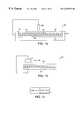
- FIG. 1 ashows a cross-sectional view of a display according to one embodiment of the invention.
- FIG. 1 bshows a partial cross-sectional view of a display according to one embodiment of the invention.
- FIG. 1 cis a chart providing two series of triboelectric elements.
- FIG. 2shows a cross-sectional view of a stylus for addressing a display according to one embodiment of the invention.
- FIG. 3 ashows a cross-sectional view of a stylus for addressing a display according to one embodiment of the invention.
- FIG. 3 bshows a bottom view of the stylus of FIG. 3 a.
- FIG. 4 ashows a schematic view of a stylus for addressing a display according to one embodiment of the invention.
- FIG. 4 bshows a cross-sectional view of a stylus for addressing a display according to one embodiment of the invention.
- FIG. 4 cshows a cross-sectional view of a stylus for addressing display according to one embodiment of the invention.
- FIG. 4 dshows a cross-sectional view of a stylus for addressing a display according to one embodiment of the invention.
- FIG. 4 eshows a schematic view of a stylus for addressing a display according to one embodiment of the invention
- FIG. 5shows a cross-sectional view of a display according to one embodiment of the invention.
- FIG. 6shows a perspective view of a display according to one embodiment of the invention.
- FIG. 7 ashows a perspective view of a display according to one embodiment of the invention.
- FIG. 7 bshows a perspective view of a display system according to one embodiment of the invention.
- FIG. 8 ashows a perspective view of a display according to one embodiment of the invention.
- FIG. 8 bshows a simplified circuit diagram of the display of FIG. 8 a.
- FIGS. 9 ashows a perspective view of a display used with a writing implement according to one embodiment of the invention.
- FIG. 9 bshows a perspective view of a display comprising a drawing made with the writing implement of FIG. 9 a according to one embodiment of the invention.
- FIG. 9 cshows a plan view of a writing implement according to one embodiment of the invention.
- FIG. 9 dshows a cross-sectional view of a drawing implement and a stylus according to one embodiment of the invention.
- FIG. 10shows a cross-sectional view of a display according to one embodiment of the invention.
- FIG. 11shows a perspective view of a display according to one embodiment of the invention.
- FIG. 12 ashows a plan view of a display according to one embodiment of the invention.
- FIG. 12 bshows a cross-sectional view of a portion of a display according to one embodiment of the invention.
- FIG. 13shows a cross-sectional view of a portion of a display according to one embodiment of the invention.
- FIG. 14 ashows a cross-sectional view of a portion of a display according one embodiment of the invention.
- FIG. 14 billustrates the rear electrodes of the display of FIG. 14 a.
- FIG. 14 cshows a cross-sectional view of a portion of a display according one embodiment of the invention.
- FIG. 15 ashows a cross-sectional view of a display according to one embodiment of the invention.
- FIG. 15 bshows a perspective view of a display according one embodiment of the invention.
- FIGS. 16 a - 16 fshow various methods of addressing a display with an electrode.
- FIG. 17shows a cross-sectional view of a display according to one embodiment of the invention.
- a display 10includes a casing 12 , a rear electrode 14 disposed inside the casing 12 , an encapsulated display media 16 disposed adjacent the rear electrode 14 , a protective layer 18 disposed adjacent the display media 16 , and a movable electrode 20 .
- the display 10can be used as a drawing system.
- the protective layer 18serves as a drawing surface.
- the movable electrode 20comprises a charge conducting mechanism.
- the movable electrode 20is a writing device.
- the writing device 20comprises a stylus.
- the display 10 of the present inventioncan be addressed mechanically by means of a robotic arm or charge-carrying print head that is moved relative to the drawing surface.
- an electrostatic printercan be used to draw on the drawing surface.
- the movable electrode 20 contacts the drawing surface 18the movable electrode 20 and the rear electrode 14 apply an electric field across the display media 16 , and thereby display an image on the drawing surface 18 of the system 10 .
- the casing 12is made from a plastic container capable of holding the display media 16 , the rear electrode 14 , and any necessary electronics.
- the casing 12can be made of any other material.
- the casing 12may be of any size, ranging from small for toy applications and large for applications in presentation displays.
- the casing 12can also include compartments for storing the drawing instrument 20 and other accessories such as an eraser.
- the encapsulated display media 16includes a particle-based display media.
- the particle-based display mediais made from an electronic ink.
- An electronic inkis an optoelectronically active material which comprises at least two phases: an electrophoretic contrast media phase 17 and a coating/binding phase 19 .
- the electrophoretic phase 17includes, in some embodiments, a single species of electrophoretic particles dispersed in a clear or dyed medium, or more than one species of electrophoretic particles having distinct physical and electrical characteristics dispersed in a clear or dyed medium.
- the electrophoretic phase 17is encapsulated, that is, there is a capsule 13 wall phase between the two phases.
- the optical quality of an electronic inkis quite distinct from other electronic display materials.
- the most notable differenceis that the electronic ink provides a high degree of both reflectance and contrast because it is pigment based (as are ordinary printing inks).
- the light scattered from the electronic inkcomes from a very thin layer of pigment close to the top of the viewing surface. In this respect it resembles an ordinary, printed image.
- electronic inkis easily viewed from a wide range of viewing angles in the same manner as a printed page, and such ink approximates a Lambertian contrast curve more closely than any other electronic display material. Since electronic ink can be printed, it can be included on the same surface with any other printed material, including traditional inks.
- Electronic inkcan be made optically stable in all display configurations, that is, the ink can be set to a persistent optical state. Fabrication of a display by printing an electronic ink is particularly useful in low power applications because of this stability.
- a capsule 13is filled with a plurality of particles and a dyed suspending fluid.
- the particlesare titania particles.
- a direct-current electric field of the appropriate polarityis applied across the capsule 13 , the particles move to the drawing surface 18 and scatter light.
- the applied electric fieldis reversed, the particles move to the rear surface of the display media 16 and the drawing surface then appears dark.
- the capsule 13includes a first set of particles and a second set of particles in the capsule 13 .
- the first set of particles and the second set of particleshave contrasting optical properties.
- the first set of particles and the second set of particlescan have differing electrophoretic mobilities.
- the first set of particles and the second set of particlescan have contrasting colors.
- the first set of particlescan be white, while the second set of particles can be black.
- the capsulefurther includes a substantially clear fluid.
- the capsulehas a rear electrode 14 on one side and a writing instrument comprising an electrode on the other side.
- the electrodes 13 , 20are connected to a source of voltage (not shown), which may provide an alternating-current (AC) field or a direct-current (DC) field to the capsule 13 .
- a source of voltagenot shown
- ACalternating-current
- DCdirect-current
- the display media 16is formed with a suspended particle display media.
- the suspended particle display mediaincludes needle-like particles in a transparent fluid. The particles change their orientation upon application of an AC field across the electrodes. When the AC field is applied, the particles are oriented perpendicular with respect to the drawing surface 18 and the surface appears transparent. When the AC field is removed, the particles are randomly oriented and the display drawing surface 18 appears opaque.
- Electronic ink displaysare novel in that they can be addressed by DC voltages and draw very little current.
- the conductive leads and electrodes used to deliver the voltage to electronic ink displayscan be of relatively high resistivity.
- the ability to use resistive conductorssubstantially widens the number and type of materials that can be used as conductors in electronic ink displays.
- ITOindium tin oxide
- the use of costly vacuum sputtered indium tin oxide (ITO) conductorsa standard material in liquid crystal devices, is not required.
- the replacement of ITO with other materialscan provide benefits in appearance, processing capabilities (printed conductors), flexibility, and durability.
- the printed electrodesare in contact only with a solid binder, not with a fluid layer (like liquid crystals).
- conductive materialswhich would otherwise dissolve or be degraded by contact with liquid crystals, can be used in an electronic ink application.
- These conductive coatingsinclude conducting or semiconducting colloids, examples of which are indium tin oxide and antimony-doped tin oxide.
- Organic conductorspolymeric conductors and molecular organic conductors also may be used.
- Polymersinclude, but are not limited to, polyaniline and derivatives, polythiophene and derivatives, poly3,4-ethylenedioxythiophene (PEDOT) and derivatives, polypyrrole and derivatives, and polyphenylenevinylene (PPV) and derivatives.
- Organic molecular conductorsinclude, but are not limited to, derivatives of naphthalene, phthalocyanine, and pentacene.
- Polymer layerscan be made thinner and more transparent than with traditional displays because conductivity requirements are not as stringent.
- the display media 16includes a binder material which binds the capsules 17 together.
- the binderis used as a non-conducting, adhesive medium supporting and protecting the capsules, as well as binding the electrode materials to the capsule dispersion. Binders are available in many forms and chemical types.
- the coating/binding phase 19includes, in one embodiment, a polymer matrix that surrounds the electrophoretic phase 17 .
- the polymer in the polymeric binderis capable of being dried, crosslinked, or otherwise cured as in traditional inks, and therefore a printing process can be used to deposit the electronic ink onto a substrate.
- the binder materialcan be water-soluble polymers, water-borne polymers, oil-soluble polymers, thermoset and thermoplastic polymers, or radiation-cured polymers.
- water-soluble polymersare the various polysaccharides, the polyvinyl alcohols, N-methyl Pyrollidone, N-vinyl pyrollidone, the various Carbowax® species (Union Carbide, Danbury, Conn.), and poly-2-hydroxyethylacrylate.
- the water-dispersed or water-borne systemsare generally latex compositions, typified by the Neorez® and Neocryl® resins (Zeneca Resins, Wilmington, Mass.), Acrysol® (Rohm and Haas, Philadelphia, Pa.), Bayhydrol® (Bayer, Pittsburgh, Pa.), and the Cytec Industries (West Paterson, N.J.) HP line.
- Neorez® and Neocryl® resinsZeneca Resins, Wilmington, Mass.
- Acrysol®Rohm and Haas, Philadelphia, Pa.
- Bayhydrol®Bayhydrol®
- Cytec IndustriesWest Paterson, N.J. HP line.
- a typical application of a water-borne resin and aqueous capsulesfollows. A volume of particles is centrifuged at low speed to separate excess water. After a given centrifugation process, for example 10 minutes at 60 ⁇ G, the capsules are found at the bottom of the centrifuge tube, while the water portion is at the top. The water portion is carefully removed. The mass of the remaining capsules is measured, and a mass of resin is added such that the mass of resin is between one eighth and one tenth of the weight of the capsules. This mixture is gently mixed on an oscillating mixer for approximately one half hour. After about one half hour, the mixture is ready to be coated onto the appropriate substrate.
- thermoset systemsare exemplified by the family of epoxies. These binary systems can vary greatly in viscosity, and the reactivity of the pair determines the “pot life” of the mixture. If the pot life is long enough to allow a coating operation, capsules may be coated in an ordered arrangement in a coating process prior to the resin curing and hardening.
- Thermoplastic polymerswhich are often polyesters, are molten at high temperatures.
- a typical application of this type of productis hot-melt glue.
- a dispersion of heat-resistant capsulescould be coated in such a medium. The solidification process begins during cooling, and the final hardness, clarity and flexibility are affected by the branching and molecular weight of the polymer.
- Oil or solvent-soluble polymersare often similar in composition to the waterborne system, with the obvious exception of the water itself.
- the latitude in formulation for solvent systemsis enormous, limited only by solvent choices and polymer solubility.
- Of considerable concern in solvent-based systemsis the viability of the capsule itself—the integrity of the capsule wall cannot be compromised in any way by the solvent.
- Radiation cure resinsare generally found among the solvent-based systems. Capsules may be dispersed in such a medium and coated, and the resin may then be cured by a timed exposure to a threshold level of ultraviolet radiation, either long or short wavelength. As in all cases of curing polymer resins, final properties are determined by the branching and molecular weights of the monomers, oligomers and crosslinkers.
- water-reducible monomers and oligomersare, however, marketed. In the strictest sense, they are not water soluble, but water is an acceptable diluent at low concentrations and can be dispersed relatively easily in the mixture. Under these circumstances, water is used to reduce the viscosity (initially from thousands to hundreds of thousands centipoise).
- Water-based capsulessuch as those made from a protein or polysaccharide material, for example, could be dispersed in such a medium and coated, provided the viscosity could be sufficiently lowered. Curing in such systems is generally by ultraviolet radiation.
- the binder materialrenders the display media elastomeric.
- a binder material including polyurethanecan render the display media elastomeric.
- the binder materialrenders the display media brittle.
- a binder material comprising an epoxycan render the display media brittle.
- the binder materialhas ultraviolet light protective properties, for example, by incorporated ultraviolet light absorbers, such as benzotriazole derivative material, in the binder.
- a display media having an elastomeric and/or UV protective materialincreases durability and lifetime of the display 10 .
- Encapsulation of the electrophoretic suspensionserves as a superior media for use in drawing devices and as a substrate for electrostatic printing.
- the benefits of microencapsulation for such purposesderive from the polymeric nature of the microcapsule wall and surrounding binder, which offers greater structural integrity than a non-encapsulated electrophoretic suspension.
- encapsulated electrophoretic suspensionsovercomes the problems encountering by prior electrophoretic drawing devices in which support walls were used as spacers. These walls cause gaps in the image and reduce the total addressable portion of the display.
- a microencapsulated electrophoretic mediais inherently supported and does not require such imageinterrupting walls. Therefore, it is possible to achieve a continuous image tracing.
- the encapsulated display media 16can be coated directly onto a plastic substrate in a process which offers a means of economical production for large surface areas. Furthermore, encapsulated display media 16 can be made flexible or set into curves and contours. This offers new manufacturing processes and design capabilities.
- encapsulated electrophoretic drawing systemrequires some electrical charge, it operates by field effect and hence draws minimal power. Further, some electrophoretic systems exhibit bistability such that once they are addressed to a dark or light state, they stay dark or light without any further power requirement, and some systems can even maintain a gray state without power. Such images can last for several months or more without requiring any further power.
- the protective layer 18is made from lexan, polycarbonate, or mylar.
- the protective layer 18includes an ultraviolet light protective coating.
- the coatingcan be imbued with UV-protective polymer material such as polyvinylfluoride or LEXAN HP 12W (polycarbonate base) or other light stabilizing additives such as Benzotriazole or Hydroperoxide decomposer (e.g., HALS, Hindered Benzoate and Phosphite), or combination of these materials.
- the protective layer 18is a scratch resistant coating.
- the protective coating 18is made from a material, which reduces grease and oil build-up on the screen surface.
- the display 10further includes a charge-generating mechanism (not shown).
- the charge-generating mechanismcan be incorporated in the casing 14 , or the movable electrode 20 .
- the charge-generating mechanismis a battery and an electronic circuit, which is capable of increasing a voltage into a range from 20 volts to 1000 volts or more, and more preferably from 100 volts to 500 volts.
- the charge-generating mechanismincludes a circuit which automatically reduces an applied voltage to zero after a pre-determined period of time to preserve batteries.
- the charge-generating mechanismhas a safety mechanism to prevent shocking the user.
- the charge-generating mechanismcan use resistors to limit maximum current drawn from the charge-generating mechanism.
- the resistanceshould be sufficient to keep the generated current to a level below that which can be felt by the user.
- the charge-generating mechanismcan have an interlock mechanism.
- the interlock mechanismprevents the user from simultaneously contacting the writing instrument and another charge-carrying device such as an eraser to be described.
- another charge-carrying devicesuch as an eraser to be described.
- at least one of the terminals of the writing instrument and the erasercan be adapted to disconnect when the user comes in contact with both.
- the display 10includes means for generating an electrostatic charge, such as Van de Graff generator, fluid pumps, or triboelectric forces.
- a Van de Graff generatorgenerates high voltage by providing physical separation of charge through a belt.
- a fluid pumpgenerates high voltage by providing physical separation of charge through fluid displacement.
- FIG. 1 billustrates a display 10 ′ using a triboelectric force.
- the system 10 ′includes a rear electrode 14 ′ in electrical communication with a slider 3 .
- the slider 3slides across the protective layer 18 ′, thereby generating a static charge.
- the static chargecan be stored in a capacitor and discharged as the user writes. This embodiment does not require a battery.
- FIG. 1 cis a chart providing two series of triboelectric elements from which an appropriate slider material and the protective layer can be selected.
- the display 10has an intervening dielectric layer.
- the dielectric layercan be placed between the protective layer 18 and the display media 16 , be incorporated into the protective layer 18 , or be incorporated into the binder material.
- the dielectric layercan store electric charge long enough to address the display media, without bleeding the charge.
- the dielectric layeralso allows applied voltage to pass through the layer and reach the display media. In this manner, the writing speed on the writing device can be increased, since the writing device need not be positioned above the display media for a duration necessary to address the display media.
- the dielectric layeris fabricated from a cross-linked polymer layer.
- the dielectric layeris fabricated from a film made of, for example, polyethylene phthalate, polyethylene naphthalate, polypropylene, polyethylene, polyvinylchloride, polysulfone, polyphnylene oxide, ionomer, polycarbonate, nylon or fluororesin layered with a bond or adhesive or such.
- a stylus 20 ′comprises an elongated probe 22 with a tip 24 .
- the tip 24may be shaped small to permit drawing of a fine line.
- the tip 24includes an electrode 26 which is flush with a surface of the tip 24 .
- the electrode 26encompasses a smaller area than the tip 24 .
- the electrode 26is connected to a voltage source (not shown) through a wire 21 .
- the tip 24is rounded. This configuration of the stylus 20 ′ permits a wider area of the stylus 20 ′ to come into contact with a drawing surface, while allowing a fine line to be drawn without puncturing the drawing surface.
- the electrode 26is covered with a dielectric coating, which protects the stylus 20 ′ and prevents exposure of the electrode 26 to the environment.
- the tip 24 of the stylus 20 ′comprises an elastomeric material.
- the stylusincludes a damping mechanism such as a spring built into the tip as to cushion the drawing surface from the physical forces caused by the motion of the user's hand.
- a damping mechanismsuch as a spring built into the tip as to cushion the drawing surface from the physical forces caused by the motion of the user's hand.
- FIGS. 3 a and 3 bdepict another embodiment in which a stylus 20 ′′ includes multiple electrodes 26 a , 26 b , 26 c , that are insulated from each other.
- a voltagecan be applied to all or any of the electrodes 26 a , 26 b , 26 c , thereby controlling the width and shape of the line drawn on the drawing surface. For example, when an electric field is applied through only the electrode 26 a, a thin line is drawn on the drawing surface. However, when an electric field is applied through both the electrodes 26 a , 26 b , a thicker line is drawn, and even a thicker line is drawn when an electric field is applied through all three electrodes 26 a , 26 b , 26 c .
- the stylus 20 ′′includes a switch 25 , and a logic circuit 27 which activates the various electrodes 26 a , 26 b , 26 c.
- the width of the line drawn on the drawing systemis controlled by varying the voltage potential applied across the display media.
- the duty cycle or the magnitude and/or duration of voltage appliedcan be varied.
- FIGS. 4 a - 4 cdepict other embodiments in which a stylus 30 includes a charge generating device 32 and/or charge-storage device 34 .
- the charge-generating devicecan be a piezo electric device 32 , 32 ′, 32 ′′ and the charge storage device can be a capacitor 34 , 34 ′, 34 ′′.
- the display 10 ′′can include a voltage source 5 and a charge storage device 34 external to the stylus 30 , as illustrated in FIG. 4 e . Referring to FIG.
- pressing the stylus 30 ′ against the drawing surface through a natural drawing motionmechanically triggers the piezo electric device 32 ′ to generate a current and to charge the capacitor 34 ′.
- a switch 35 on the stylus 30 ′′can be clicked to trigger the piezo electric device 32 ′ to generate a current and to charge the capacitor 34 ′′.
- the stylusincludes a switch which permits the user to reverse the electric field applied across the display media, and thereby switch from drawing in one color to drawing in another color.
- the second colormay have the effect of erasing what is drawn using the first color.
- the usercan draw in blue on a white background prior to switching, and draw in white on a blue background after switching.
- the voltage applied to the electrode 36can switch from +100 v to ⁇ 100 v, where the voltage applied to the rear electrode of the drawing device is 0 v.
- the voltage applied to the electrode 36 of the stylus 30can remain 0 v and the voltage applied to the rear electrode varied.
- the stylus 40includes two electrodes 42 , 44 placed at opposite ends of the stylus 40 .
- Different voltagesare applied to each of the electrodes 42 , 44 , such that electrode 42 allows the user to draw in one color, while electrode 44 allows the user to draw in a different color.
- a positive voltagecan be applied to electrode 42 to write on the drawing surface, while a negative voltage of the same magnitude can be applied to electrode 44 to erase the drawing on the drawing surface.
- the switch 45allows the user to select one of the two electrodes 42 , 44 .
- the rear electrodeis set to ground.
- a display 50includes a casing 52 , a rear electrode 53 disposed inside the casing 52 , an encapsulated display media 54 disposed adjacent the rear electrode 53 , a piezoelectric film 56 disposed adjacent the display media 54 , and a protective layer 55 disposed adjacent the piezoelectric film 56 .
- the stylus 58need not be electrically connected to the drawing device 50 or include a charge generator.
- the piezoelectric film 56becomes charged.
- the piezoelectric 56 filmcan comprise a polymeric material.
- the piezoelectric filmcan comprise vinylidene fluoride homopolymer or a copolymer of vinylidene fluoride and one or more copolymerizable monomers.
- the display media 54includes capsules, each capsule comprising a plurality of particles dispersed in a fluid medium.
- a drawing system 60which is substantially similar to the display of FIG. 1 a further includes a piezo electric button 62 connected to a capacitor 68 .
- the capacitoris connected to the stylus 69 .
- the system 60can further include means for mechanically storing energy using, for example, a spring and subsequently transferring the mechanical energy to the piezo electric device 62 .
- a drawing system 70which is substantially similar to the display of FIG. 1 a further includes an eraser 72 .
- the eraser 72is physically connected to the drawing system 70 through a cable 73 .
- An image created on the drawing surface 71 by applying an electric field across the display media of the drawing system 70 through the writing instrument (not shown) and the rear electrode (not shown)can be erased by applying an oppositely charged electric field across the display media through the eraser 72 and the rear electrode.
- the eraser 72 ′is positioned inside the device casing 74 above the drawing surface 71 in the form of a sliding bar 76 as shown in FIG. 7 b .
- the sliding bar 76includes a tab 78 , which the user can use to slide the eraser bar 76 across the drawing surface 71 , thereby erasing an image drawn on the drawing surface 71 .
- the sliding bar 76has an electrode which can be set to positive or negative voltage to cause the screen to change its color.
- a drawing system 80includes a casing 82 , a rear electrode, an encapsulated display media, a protective layer, and an electrode surface 84 .
- the protective layer 85functions as the drawing surface.
- a usertouches the electrodes surface 84 with his or her first hand 86 , while the user writes on the drawing surface 85 with the second hand 88 .
- a separate writing instrumentmay not be necessary.
- a voltage sourceis placed inside the casing 82 . Since the human body is electrically conductive, an electric field can be created across the display media through the user's second hand 88 and the rear electrode. As illustrated in FIG. 8 b , a typical skin resistance is about 10 k ⁇ -500 k ⁇ .
- the drawing system 80has an internal 1 m ⁇ current limiting resistor (R CL ) When 100 V is applied, the resistor (R CL ) would limit current flowing though the body and the display system to 100 k ⁇ .
- the electrode surface 84can be a button. Alternatively, the electrode surface 84 can be a part of a stylus.
- the movable electrode of the present inventioncan have a variety of shapes or forms to provide different drawing tips.
- the movable electrodecan include a calligraphic tip, brush, sponge, fabric, roller, or elastomeric solid, which is electrically connected to a source of charge such an electrode surface, a voltage source, or a stylus.
- the writing instrumentcan comprise a non-conductive object coated with a conductive layer.
- the writing instrumentcan be cones, shapes and cards.
- the movable electrodecan comprise a stamp in any shape or form.
- a writing implement 90can be used with the drawing system of the present invention.
- the writing implement 90can be in the form of a card.
- the writing implement 90includes an invisible conductive pattern 92 printed on the back side of the card.
- the writing implement 90is placed on a drawing surface 93 of the drawing system 94 a and a voltage is applied to the conductive pattern 92 using a stylus 95 , the conductive pattern leaves a surprise image 96 on the drawing surface 93 .
- the writing implement 90includes a cut out hole 91 in the form of letter A.
- this writing implement 90When using this writing implement 90 , the user places the writing implement 90 on the drawing surface 93 and fills in the letter A using the stylus. An edge of the cut out hole 91 includes a conductor 97 which is connected to the conductor pattern 92 . Thus, when the stylus contacts the conductor 97 , a surprise image 96 corresponding to the conductor pattern 92 appears on the drawing surface.
- the drawing implement 90is removed from the drawing surface 93 , the letter A remains, but next to it a picture of an apple 96 is also shown. The embodiment can be useful as a teaching tool for children.
- FIG. 10depicts an embodiment in which a display 100 has both erasable and non-erasable portions for flexibility.
- the display 100includes a casing 102 , a rear electrode 104 , an encapsulated display media 106 , a top electrode 108 , a protective layer 109 , and a stylus 107 .
- a first portion of the drawing device 100is available for the user to draw on, while a second portion of the drawing device 100 provides a predetermined image.
- the top electrode 108 and the rear electrode 104apply an electric field across the display media 106 .
- an animated figurecan be provided on the drawing surface 109 using this embodiment.
- a figure holding a “BLUE” signcan appear when the stylus 107 is set to draw in blue, and the “WHITE” sign can appear when the stylus 107 is set to draw in white.
- the display of the present inventioncan be integrated with other multimedia elements including audio feedback tones or music, to enhance the drawing experience.
- a speaker included in the displaycan emit sound when the stylus is toggled from a first voltage to a second voltage.
- a display 110provides multiple drawing surfaces.
- the display 110includes a casing 112 , a flexible display media 114 arranged in a continuous belt loop, a rear electrode 116 disposed inside the belt loop, and a protective layer 118 serving as a drawing surface
- the display media 114loops around a pair of rollers 119 and a knob 117 for rolling the belt loop.
- the usercan roll between different drawing surfaces. For examples the user can draw on the first drawing surface of the display media, 114 a , then roll it to the back in order to save the drawing, and still have another fresh drawing surface, 114 b .
- the display media 114comprises an encapsulated electrophoretic display media
- the first drawing surface of the display media, 114 aprovides a first color combination such as black and white
- the second drawing surface of the display media, 114 bprovides a second color combination such as yellow and blue
- the display 110further includes an elaser 113 , which erases the surface of the display media 114 as it rolls back.
- a display of the present inventionis flexible.
- the flexible displayis used as a wallpaper which provides a drawing surface.
- the displaycan be constructed by coating a transparent protective layer with an encapsulated electrophoretic display media and then laminating this coated structure with a rear electrode.
- Examples of flexible, transparent protective layerinclude polyester, polycarbonate, polyvinylfluoride, acrylic, and polychlorotriflouroethylene.
- the rear electrodecan comprise a flexible polymeric conductor material such as conductive particle doped with polymers, conductive polymers (e.g., polyaniline, polyacetylene, polythiophene), doped polymers, metallized polymers, or polymer film coated with conductive material (e.g., metal, metal oxide, conductive particle dispersion, and conductive polymer dispersion).
- conductive polymerse.g., polyaniline, polyacetylene, polythiophene
- doped polymerse.g., polyaniline, polyacetylene, polythiophene
- metallized polymerse.g., polymer film coated with conductive material (e.g., metal, metal oxide, conductive particle dispersion, and conductive polymer dispersion).
- conductive materiale.g., metal, metal oxide, conductive particle dispersion, and conductive polymer dispersion
- the flexible displaycan be used as an “electronic paper.”
- An electronic papercan be used anywhere paper is used today but offers the ability to be updated via stylus, printhead or similar means.
- An electronic papercan be used as reusable fax and copier paper, re-writable bar-codes, labels and packaging, re-writable displays on plastic cards, credit cards, laminated driver's licenses and magnetic strip cards, reprintable signs and billboards, and reusable newspapers, magazines, greeting cards and books.
- the encapsulated display media or the display media in combination with the rear electrode of the drawing systemcan be removed and replaced with a fresh display media or display media/rear electrode combination by the user, such that the user can keep his or her drawings.
- the rear electrode of the drawing systemcan be removed and replaced with a different rear electrode.
- the systemmay include a connector which provides electrical communication between a voltage source and the rear electrode.
- These removable electrodeswould permit a variety of rear electrode patterns to be used with the drawing system.
- the electrodecan be patterned to include a first section connected to the ground and a second section connected to the stylus potential.
- the first section connected to groundcan be revealed when the stylus is placed adjacent the first section.
- This embodimentcan be used to create a coloring book.
- an outlinecan be provided on the drawing surface using this embodiment.
- the userfirst sets the entire drawing surface to display a single color such as blue.
- a rear electrode having a non-conductive pattern of an outline such as a mapis inserted in the drawing system.
- An electric fieldis applied to the display media of the drawing system to change the color of the display from blue to another color, such as white.
- the outline of the mapremains in blue, while the rest of the display becomes white.
- the usercan now write on the drawing surface in blue and may write visibly over the map shown on the drawing surface.
- a drawing system 120permits the user to write using a stylus or a charge-generating electrostatic print head 124 .
- an electrostatic print head 124is moved across a fixed electrophoretic display media to create an image.
- the electrostatic print head 124senses its location on the drawing system 120 such that it can print locally on the display surface.
- the drawing system 120in this embodiment, can be used as a printer.
- the electrostatic print head 124can move automatically or manually.
- the system 120can further include a speed sensor for detecting manual scanning of the print head.
- a drawing systememploys both electrophoretic effect and other means to permit a user to draw on the system.
- the system 125includes a casing 126 , an encapsulated display media 127 in the form of a belt loop, a rear electrode 128 disposed within the belt loop, and a protective coating 129 .
- the system 125further includes an electrostatic printer 123 for providing an underlying image on the drawing surface 129 .
- the usercan use a standard dry-erasable marker 121 to draw on the drawing surface 129 as is typically used on white boards. Both the underlying image and the user's markings are visible on the drawing surface 129 .
- the drawing system 125further includes an optical input means (e.g., scanner) for scanning a drawing provided by the standard dry-erasable marker 121 .
- the drawing systemincludes a first region which displays a permanent image and a second region in which the user can write on and erase.
- the drawing systemcan include a blank map or a blank calendar.
- the drawing system 130includes the rear electrode separated into multiple regions 132 , 134 .
- the first region 132has a voltage equal to the voltage of the stylus 136 , such that an electric field cannot be applied across the display media 138 adjacent the first region 132 . Therefore, the user cannot write on or erase on the first region 132 .
- the second region 134has a voltage different from the voltage of the stylus 136 , such that an electric field can be applied across the display media 138 adjacent the second region 134 .
- the userdraws on the second region 134 .
- the drawing system 130can include a rear electrode having an electrode pattern corresponding to an image to be permanently displayed on the drawing system 130 .
- the drawing system 140provides multiple optical properties, such as permitting the user to draw in multiple colors.
- the drawing system 140includes a pixelated rear electrode 144 .
- the rear electrode 144is patterned into multiple pixel or line electrodes 144 a , 144 b , 144 c .
- the pixel or line electrodes 144 a , 144 b , 144 chave a width of less than about 1 mm.
- the first electrodes 144 acorrespond to a first optical property (e.g., red)
- the second electrodes 144 bcorrespond to a second optical property (e.g., green)
- the third electrodes 144 ccorrespond to a third optical property (e.g., blue).
- the drawing system 140further includes an encapsulated display media 146 , which includes particles or solvent of different optical properties, such as color.
- the display media 146can include particles or solvent of red, green, and blue, or cyan, magenta, and yellow.
- a capsule adjacent the first electrode 144 aincludes white particles and a red dye
- a capsule adjacent the second electrode 144 bincludes white particles and a green dye
- a capsule adjacent the third electrode 144 cincludes white particles and a blue dye.
- the display media 146 adjacent the first electrode 144 aforms a red region 146 a .
- the display media 146 adjacent the second electrode 144 bforms a green region 146 b .
- the display media 146 adjacent the third electrode 144 cforms a blue region 146 c.
- a voltage which differs from the voltage of the stylus 148is applied to the pixel or line electrodes 144 a corresponding to red.
- the electrodes 144 aare connected to a common red electrode.
- the stylus 148 and the rear electrodes 144 aestablish an electric field across the display media 146 , such that white particles migrate away from the protective layer 149 and displaying the color of the red dye.
- a voltage that matches the voltage of the stylus 148is applied to the pixel or line electrodes 144 b , 144 c corresponding to green and blue, such that an electric field across the green region 146 b and the blue region 146 c cannot be established.
- the second electrodes 144 bare connected to a common green electrode.
- the third electrodes 144 care connected to a common blue region.
- the stylus 148does not electrophoretically affect any media except the media corresponding to the red regions 146 a .
- various color effectssuch as color combinations may be achieved.
- a pixelated rear electrodeis created by providing a dielectric substrate of one or more layers in which multiple electrodes corresponding to the same color are provided on a single layer and connected in parallel.
- the pixelated electrodescan be provided on a single substrate.
- the drawing system 150includes a display media 154 comprising a red region 154 a , a green region 154 b , and a blue region 154 c as substantially described with respect to FIG. 14 a , and a movable rear electrode 152 which addresses one of the three regions 154 a , 154 b , 154 c at a time.
- a movable rear electrode 152When the movable rear electrode 152 is placed adjacent a region, an electric field is applied to that region to display the color of that region.
- a mechanical switchcan be used to move the electrode.
- FIGS. 14 a and 14 bare provided as examples only. Other embodiments for providing a color display can be used in accordance with the present invention.
- Commonly-owned, co-pending U.S. patent application Ser. No. 09/140,862 filed Aug. 27, 1998, which describes color electrophoretic displaysis incorporated herein by reference.
- a display 200includes a rear electrode 202 , a display media 204 , a front electrode 206 , and a touchscreen 208 .
- the touchscreen 208is disposed adjacent the front electrode 206 .
- the touchscreen 208can be laminated to or integrated with the display media 204 .
- one of the electrodes of the touchscreencan be applied directly on the front electrode 206 of the display 200 .
- Touchscreenswhich operate through resistive and capacitive effects are known to those skilled in the art.
- the display 200is activated when a drawing instrument is pressed against the touchscreen 208 .
- the touchscreencan be positioned behind the drawing system.
- the display of the present inventionis incorporated into a data capture mechanism, such as a credit card authorization terminal.
- a usersigns his or her signature on a drawing surface of the display, and his or her signature is captured and digitized.
- the stylus or data sourceemits wireless waves that are received by a sensing mechanism underneath the microencapsulated electrophoretic layer and bottom electrode.
- the flexibility of the microencapsulated electrophoretic layeris utilized to permit localized pressure to transfer through the display media to a pressure-sensitive array or touch screen-type device in front of or behind the display media.
- One advantage of this embodimentis that while the signature or data tracing may be digitized at a coarse resolution, its image is displayed in analog by the display media at higher resolutions.
- the stylus or data sourceemits infrared or visible signals that transfer through the display media to a sensing mechanism; here the wide temperature operating range of microencapsulated electrophoretic displays is useful.
- the stylustransmits acoustic waves that are again sensed by a mechanism behind the display media.
- the sensing mechanism describe abovecan provide information about the location of the instrument on the display.
- the display 160includes an electrostatic printing mechanism.
- the electrostatic printing mechanismis included in a sliding bar 162 , which may have one or more electrodes.
- the electrodesare connected to a driving mechanism such as an integrated circuit.
- the electrodescan also be connected to a data source such as a data storage device or a communications device.
- the communications devicecan be, for example, a pager, a receiver, a modem, an infrared port or direct cable connection.
- the sliding bar 162can further include logic circuitry and position sensors.
- the sliding barcan be used as a manual or automatic electrostatic print head and can transfer images to the drawing screen when the user slides the sliding bar 162 .
- the system 100can further include mechanical or optic speed sensing device to detect the manual scanning of the print head.
- the display 160 of FIG. 15 ballows a user to download and display an image on the drawing screen.
- the imagecan be text (newspaper, book, e.g.), a dotted line image, a partial image, an image from a scrapbook or database, or even an interactive series of images.
- the drawing deviceWhen equipped with a communications device and appropriate logic circuitry, the drawing device thereby can serve as a low-cost information display device such as an extremely cheap web browser.
- the sliding bar 162supports a scanning device.
- the scanning devicecan digitize the image provided on the screen of the drawing system. When used in combination with a data storage device, memory device, or communications device, this will allow the drawing system to store, recall and transmit images.
- an external scanning devicecan be used with the display 10 system.
- the sliding bar 162slides across the screen as shown in FIG. 16 a or is manually moved across the screen as shown in FIG. 16 g to erase, scan, or draw.
- the screen of the drawing systemcan be moved relative to an electrode to perform the same functions.
- the screencan be provided in a conveyor belt-like construction, where the screen moves as shown in FIG. 16 b , or where the electrode moves as shown in FIG. 16 d .
- the screencan be pulled out of a roll of display media as with a window shutter as shown in FIG. 16 f , or the screen can be pulled through the sliding bar from side to side as shown in FIGS. 16 c and 16 e.
- a display system 170includes a clear rear conductive electrode 172 , a photoconductive dispersion layer 173 , an encapsulated display media 174 , and a top electrode 176 .
- the display system 170can “pick up” images from light-reflecting or light-emitting sources.
- the light 178 from an image displayed on a light-reflecting or light-emitting sourcestrikes the photoconductive layer 173 , causing the rear electrode 172 along with the top electrode 176 to apply an electric field across the display media 174 , and thereby reproduce the picked up image on the display system 170 .
- the means for generating the electric fieldcan be built internally or externally to the display system.
- the system 170can further include a light source (e.g., fluorescent light) for illuminating the substrate which reflects the light.
- the light-reflecting substratecan be paper.
- the user of the display system 170can hold the display system 170 up to a light emitting display, such as a television or computer screen, move a sliding bar described above (not shown) across the top surface of the system 170 , and thereby cause the display system 170 to reproduce the image on the television or computer screen.
- a light emitting displaysuch as a television or computer screen
- the usersimply places the display system 170 in front of the television or computer screen to capture the image shown on the television or computer screen.
- a light source internal or external to the display system 170can illuminate a substrate and capture light-reflecting from the substrate, thereby copying the image on the substrate.
- Such systemcan be used as a toy, or as a novel way of transporting temporary images. For instance, a user can hold an electronic paper to his or her computer screen, image his or her day's agenda, and then carry this paper throughout the day.
- the term “display” and the term “drawing system”have been used interchangably herein. Both terms include devices capable of providing drawing, copying, printing, or erasing functions.
- the term “movable electrode” as used hereinincludes a writing device, an eraser, a printer, or a scanner.
- the “movable electrode”also refers to an electrode capable of moving relative to a display surface by either moving the electrode or moving the display.
Landscapes
- Physics & Mathematics (AREA)
- Nonlinear Science (AREA)
- General Physics & Mathematics (AREA)
- Optics & Photonics (AREA)
- Chemical & Material Sciences (AREA)
- Engineering & Computer Science (AREA)
- Crystallography & Structural Chemistry (AREA)
- Mathematical Physics (AREA)
- Theoretical Computer Science (AREA)
- Health & Medical Sciences (AREA)
- Life Sciences & Earth Sciences (AREA)
- Chemical Kinetics & Catalysis (AREA)
- Electrochemistry (AREA)
- Molecular Biology (AREA)
- Electrochromic Elements, Electrophoresis, Or Variable Reflection Or Absorption Elements (AREA)
- Toys (AREA)
Abstract
Description
This invention claims priority to provisional application U.S. Ser. No. 60/085,096 filed on May 12, 1998.
This invention is related to a display device, and more specifically to a drawing device.
An erasable drawing device is known. An erasable drawing device, typically, consists of a blackboard, paper pad, or white board, and an erasable marking device such as a chalk, pencil or dry-erasable marker.
One drawback of such drawing device is that the marking device can dissipate, requiring replacement. Another drawback is that the marking device can make marks on surfaces other than the screen of the drawing device, thereby creating a mess. Still another drawback is that the screen may not erase completely even with cleansers and vigorous erasing.
An electronic drawing device overcomes some the problems described above. An electronic drawing device, typically, includes a touch screen and appropriate logic to cause an underlying electronic display to update its image in response to the motion of a stylus. The device, for example, includes a graphics input pad having an array of transparent capacitive pixels, which change their capacitance in response to a conductive tipped stylus passing over the pad. The change in capacitance is sensed and used to address an LCD matrix. A drawback of this electronic drawing device is that it requires sophisticated electronics and significant amount of power. U.S. Pat. No. 4,639,720 describes an electronic drawing device.
A magnetophoretic display, typically used as children's drawing toy, is another example of an erasable drawing device. In a magnetophoretic display, a stylus used to write on the display contains a magnet, and a contrast media on the display contains black ferrous material and white titanium dioxide. The magnetophoretic display requires no power. However, the magnetophoretic display does not typically permit the user to selectively erase portions of a drawing on the display, unless the user is able to access both the front and back of the magnetophoretic media. Typically, manufacturers of magnetophoretic displays simply provide access to only one surface. The display is erased using a sliding bar magnet embedded behind the magnetophoretic media. Therefore, the display cannot be selectively erased.
An electrostatically-addressed liquid crystal display is another type of drawing device known in the art. Liquid crystal drawing devices, however, suffer from poor image duration due to dissipation of the surface static charge which maintains the image. With higher voltages and additional resistive layers, it is possible to extend image duration, but even then, a duration exceeding 30 minutes is considered state of the art. U.S. Pat. Nos. 5,351,143 and 5,117,297, describe liquid crystal drawing devices.
An electrophoretic display is also used as a drawing device. In an electrophoretic drawing device, electrophoretic particles in a display media of the device migrate toward or away from the drawing surface of the device upon application of an electric field across the display media. For example, the drawing device can contain a back electrode covered by an electrophoretic coating. To write, a positive voltage is applied to the back electrode and a stylus contacting the electrophoretic coating is set at ground. The stylus acts as a top electrode in a local area. A voltage potential is created between the stylus and the back electrode which causes migration of the electrophoretic particles and a color change of the device. The overall system may be covered with a dielectric or anisotropic top layer that protects the electrophoretic media. Chiang et al. “A Stylus Writable Electrophoretic Display Device,” Society for Information Display 1979 Digest describes an electrophoretic drawing device. Although electrophoretic displays offer excellent contrast and brightness as well as favorable electrical properties and image duration, electrophoretic displays have not been broadly commercialized due to difficulty in manufacture and lifetime issues related to particle agglomeration and migration within the display.
In one aspect, the invention features a display. In one embodiment, the display comprises an encapsulated display media having a first surface and a second surface, a rear electrode disposed adjacent the second surface of the display media, and a movable electrode. The display media comprises a plurality of capsules, each capsule comprising a plurality of particles dispersed in a fluid. The movable electrode, in conjunction with the rear electrode, applies an electric field across the display media.
In one detailed embodiment, the movable electrode comprises a writing device. The writing device can comprise a charge generator. The charge generator can comprise an electronic circuit capable of increasing a voltage from about 20 V to about 1000 V. The charge generator can further comprise an electronic circuit, which reduces an applied voltage to zero after a predetermined time interval. The writing device can comprise a charge storage device. The writing device can comprise a stylus. For example, the stylus can comprise an electrode tip disposed within a curved end of the stylus. The stylus can further comprise a plurality of concentric electrodes. The writing device can include an activator, such as a piezoelectric device, which activates the charge generator. The writing device can have a first end and a second end. The display media displays a first color when the first end is disposed adjacent the first surface of the display media and a second color when the second end is disposed adjacent the first surface of the display media.
In another detailed embodiment, the movable electrode comprises an eraser. In still another detailed embodiment, the movable electrode comprises a user touching the first surface of the display media. In still another detailed embodiment, the movable electrode comprises a sliding bar, which slides across the first surface of the display media. The sliding bar can include a charge generator, an activator which activates the charge generator, an electrostatic print head, and/or a scanner. The charge generator can be a Van de Graaff device, a triboelectric mechanism, or a hand-driven electric generator. The sliding bar can communicate with a data storage device. Alternatively, the sliding bar can comprise a data storage device.
In still another detailed embodiment, the movable electrode comprises a switch, which reverses an electric field applied to the display media upon activation of the switch. For example, a color displayed on the first surface of the display media can change upon activation of the switch.
In one embodiment, the rear electrode comprises a first region having a voltage different from a voltage of the movable electrode and a second region having a voltage :matching the voltage of the movable electrode. In another embodiment, the rear electrode comprises a conductive pattern. In still another embodiment, the display media comprises a plurality of electrophoretic particles comprising a plurality of colors, and the rear electrode comprises a plurality of pixel electrodes, each pixel electrode being set at a voltage for displaying particles of a selected color on the first surface of the display media. Alternatively, the rear electrode can be movable.
In another detailed embodiment, the display further comprises a touch screen disposed adjacent the first surface or the second surface of the display media. The touch screen can be laminated to the display media.
In another embodiment, the display comprises a display media forming a continuous loop, and an electrode disposed inside the continuous loop of the display media. In one detailed embodiment, the display further comprises a case containing the display media and the electrode. The case has a first surface and a second surface. The first surface comprises a protective layer and serves as a writing surface. In another detailed embodiment, the display further comprises a movable electrode. The movable electrode, in conjunction with the electrode, applies an electric field across the display media.
In still another embodiment, the display comprises a display media having a first surface and a second surface, an electrode disposed on the first surface of the display media, and a photoconductor disposed on the second surface of the display media. The display media displays a replica of an image shown on a substrate when the photoconductor is provided adjacent the substrate. In one detailed embodiment, the substrate comprises an emissive display such as a computer screen or a television screen.
In another detailed embodiment, the substrate comprises a reflective display. The reflective display can be a piece of paper. In another detailed embodiment, the display further comprises a light source for illuminating the substrate.
In another aspect, the invention features a method for creating an image on a display. The method comprises the steps of: (a) providing a display comprising an encapsulated display media comprising a plurality of capsules, each capsule comprising a plurality of particles dispersed in a fluid, the display media having a first surface and a second surface and a rear electrode disposed on the second surface of the display media; (b) placing a movable electrode adjacent the first surface of the display media; and (c) applying an electric field across the display media through the movable electrode and the rear electrode, thereby creating an image on the first surface of the display media.
In another aspect, the invention features a method for reproducing an image. The method comprises the steps of: (a) providing a display comprising: a1) a display media comprising a first surface and a second surface, a2) an electrode disposed on the first surface of the display media, and a3) a photoconductor disposed on the second surface of the display media; and (b) placing the photoconductor adjacent a substrate comprising an image, thereby reproducing the image from the substrate on the display media.
The foregoing and other objects, features and advantages of the present invention, as well as the invention itself, will be more fully understood from the following description of preferred embodiments, when read together with the accompanying drawings, in which:
FIG. 1ashows a cross-sectional view of a display according to one embodiment of the invention.
FIG. 1bshows a partial cross-sectional view of a display according to one embodiment of the invention.
FIG. 1cis a chart providing two series of triboelectric elements.
FIG. 2 shows a cross-sectional view of a stylus for addressing a display according to one embodiment of the invention.
FIG. 3ashows a cross-sectional view of a stylus for addressing a display according to one embodiment of the invention.
FIG. 3bshows a bottom view of the stylus of FIG. 3a.
FIG. 4ashows a schematic view of a stylus for addressing a display according to one embodiment of the invention.
FIG. 4bshows a cross-sectional view of a stylus for addressing a display according to one embodiment of the invention.
FIG. 4cshows a cross-sectional view of a stylus for addressing display according to one embodiment of the invention.
FIG. 4dshows a cross-sectional view of a stylus for addressing a display according to one embodiment of the invention.
FIG. 4eshows a schematic view of a stylus for addressing a display according to one embodiment of the invention
FIG. 5 shows a cross-sectional view of a display according to one embodiment of the invention.
FIG. 6 shows a perspective view of a display according to one embodiment of the invention.
FIG. 7ashows a perspective view of a display according to one embodiment of the invention.
FIG. 7bshows a perspective view of a display system according to one embodiment of the invention.
FIG. 8ashows a perspective view of a display according to one embodiment of the invention.
FIG. 8bshows a simplified circuit diagram of the display of FIG. 8a.
FIGS. 9ashows a perspective view of a display used with a writing implement according to one embodiment of the invention.
FIG. 9bshows a perspective view of a display comprising a drawing made with the writing implement of FIG. 9aaccording to one embodiment of the invention.
FIG. 9cshows a plan view of a writing implement according to one embodiment of the invention.
FIG. 9dshows a cross-sectional view of a drawing implement and a stylus according to one embodiment of the invention.
FIG. 10 shows a cross-sectional view of a display according to one embodiment of the invention.
FIG. 11 shows a perspective view of a display according to one embodiment of the invention.
FIG. 12ashows a plan view of a display according to one embodiment of the invention.
FIG. 12bshows a cross-sectional view of a portion of a display according to one embodiment of the invention.
FIG. 13 shows a cross-sectional view of a portion of a display according to one embodiment of the invention.
FIG. 14ashows a cross-sectional view of a portion of a display according one embodiment of the invention.
FIG. 14billustrates the rear electrodes of the display of FIG. 14a.
FIG. 14cshows a cross-sectional view of a portion of a display according one embodiment of the invention.
FIG. 15ashows a cross-sectional view of a display according to one embodiment of the invention.
FIG. 15bshows a perspective view of a display according one embodiment of the invention.
FIGS. 16a-16fshow various methods of addressing a display with an electrode.
FIG. 17 shows a cross-sectional view of a display according to one embodiment of the invention.
Referring to FIG. 1a, adisplay 10 includes acasing 12, arear electrode 14 disposed inside thecasing 12, an encapsulateddisplay media 16 disposed adjacent therear electrode 14, aprotective layer 18 disposed adjacent thedisplay media 16, and amovable electrode 20. Thedisplay 10 can be used as a drawing system. Theprotective layer 18 serves as a drawing surface. Themovable electrode 20 comprises a charge conducting mechanism. In one embodiment, themovable electrode 20 is a writing device. In the embodiment of FIG. 1, thewriting device 20 comprises a stylus. Alternatively, thedisplay 10 of the present invention can be addressed mechanically by means of a robotic arm or charge-carrying print head that is moved relative to the drawing surface. For example, an electrostatic printer can be used to draw on the drawing surface. When themovable electrode 20 contacts thedrawing surface 18, themovable electrode 20 and therear electrode 14 apply an electric field across thedisplay media 16, and thereby display an image on thedrawing surface 18 of thesystem 10.
In one embodiment, thecasing 12 is made from a plastic container capable of holding thedisplay media 16, therear electrode 14, and any necessary electronics. Alternatively, thecasing 12 can be made of any other material. Thecasing 12 may be of any size, ranging from small for toy applications and large for applications in presentation displays. Thecasing 12 can also include compartments for storing thedrawing instrument 20 and other accessories such as an eraser.
In one embodiment, the encapsulateddisplay media 16 includes a particle-based display media. In one detailed embodiment, the particle-based display media is made from an electronic ink. An electronic ink is an optoelectronically active material which comprises at least two phases: an electrophoreticcontrast media phase 17 and a coating/bindingphase 19. Theelectrophoretic phase 17 includes, in some embodiments, a single species of electrophoretic particles dispersed in a clear or dyed medium, or more than one species of electrophoretic particles having distinct physical and electrical characteristics dispersed in a clear or dyed medium. In some embodiments theelectrophoretic phase 17 is encapsulated, that is, there is acapsule 13 wall phase between the two phases.
The optical quality of an electronic ink is quite distinct from other electronic display materials. The most notable difference is that the electronic ink provides a high degree of both reflectance and contrast because it is pigment based (as are ordinary printing inks). The light scattered from the electronic ink comes from a very thin layer of pigment close to the top of the viewing surface. In this respect it resembles an ordinary, printed image. Also, electronic ink is easily viewed from a wide range of viewing angles in the same manner as a printed page, and such ink approximates a Lambertian contrast curve more closely than any other electronic display material. Since electronic ink can be printed, it can be included on the same surface with any other printed material, including traditional inks. Electronic ink can be made optically stable in all display configurations, that is, the ink can be set to a persistent optical state. Fabrication of a display by printing an electronic ink is particularly useful in low power applications because of this stability.
In one embodiment, acapsule 13 is filled with a plurality of particles and a dyed suspending fluid. In one detailed embodiment, the particles are titania particles. When a direct-current electric field of the appropriate polarity is applied across thecapsule 13, the particles move to thedrawing surface 18 and scatter light. When the applied electric field is reversed, the particles move to the rear surface of thedisplay media 16 and the drawing surface then appears dark.
In another detailed embodiment, thecapsule 13 includes a first set of particles and a second set of particles in thecapsule 13. The first set of particles and the second set of particles have contrasting optical properties. For example, the first set of particles and the second set of particles can have differing electrophoretic mobilities. In addition, the first set of particles and the second set of particles can have contrasting colors. For example, the first set of particles can be white, while the second set of particles can be black. The capsule further includes a substantially clear fluid. The capsule has arear electrode 14 on one side and a writing instrument comprising an electrode on the other side. Theelectrodes capsule 13. Upon application of an electric field across theelectrodes surface 18, while the second set of particles move toward therear electrode 14.
In another detailed embodiment, thedisplay media 16 is formed with a suspended particle display media. The suspended particle display media includes needle-like particles in a transparent fluid. The particles change their orientation upon application of an AC field across the electrodes. When the AC field is applied, the particles are oriented perpendicular with respect to thedrawing surface 18 and the surface appears transparent. When the AC field is removed, the particles are randomly oriented and thedisplay drawing surface 18 appears opaque. Commonly-owned, co-pending U.S. patent application Ser. No. 09/140,792 filed on Aug. 27, 1998, which describes electrophoretic displays, is incorporated herein by reference.
Electronic ink displays are novel in that they can be addressed by DC voltages and draw very little current. As such, the conductive leads and electrodes used to deliver the voltage to electronic ink displays can be of relatively high resistivity. The ability to use resistive conductors substantially widens the number and type of materials that can be used as conductors in electronic ink displays. In particular, the use of costly vacuum sputtered indium tin oxide (ITO) conductors, a standard material in liquid crystal devices, is not required. Aside from cost savings, the replacement of ITO with other materials can provide benefits in appearance, processing capabilities (printed conductors), flexibility, and durability. Additionally, the printed electrodes are in contact only with a solid binder, not with a fluid layer (like liquid crystals). This means that some conductive materials, which would otherwise dissolve or be degraded by contact with liquid crystals, can be used in an electronic ink application. These include opaque metallic inks for the rear electrode (e.g., silver and graphite inks), as well as conductive transparent inks for either substrate. These conductive coatings include conducting or semiconducting colloids, examples of which are indium tin oxide and antimony-doped tin oxide. Organic conductors (polymeric conductors and molecular organic conductors) also may be used. Polymers include, but are not limited to, polyaniline and derivatives, polythiophene and derivatives, poly3,4-ethylenedioxythiophene (PEDOT) and derivatives, polypyrrole and derivatives, and polyphenylenevinylene (PPV) and derivatives. Organic molecular conductors include, but are not limited to, derivatives of naphthalene, phthalocyanine, and pentacene. Polymer layers can be made thinner and more transparent than with traditional displays because conductivity requirements are not as stringent.
In one embodiment, thedisplay media 16 includes a binder material which binds thecapsules 17 together. The binder is used as a non-conducting, adhesive medium supporting and protecting the capsules, as well as binding the electrode materials to the capsule dispersion. Binders are available in many forms and chemical types. The coating/bindingphase 19 includes, in one embodiment, a polymer matrix that surrounds theelectrophoretic phase 17. In this embodiment, the polymer in the polymeric binder is capable of being dried, crosslinked, or otherwise cured as in traditional inks, and therefore a printing process can be used to deposit the electronic ink onto a substrate. In another embodiment, the binder material can be water-soluble polymers, water-borne polymers, oil-soluble polymers, thermoset and thermoplastic polymers, or radiation-cured polymers.
Among the water-soluble polymers are the various polysaccharides, the polyvinyl alcohols, N-methyl Pyrollidone, N-vinyl pyrollidone, the various Carbowax® species (Union Carbide, Danbury, Conn.), and poly-2-hydroxyethylacrylate.
The water-dispersed or water-borne systems are generally latex compositions, typified by the Neorez® and Neocryl® resins (Zeneca Resins, Wilmington, Mass.), Acrysol® (Rohm and Haas, Philadelphia, Pa.), Bayhydrol® (Bayer, Pittsburgh, Pa.), and the Cytec Industries (West Paterson, N.J.) HP line. These are generally latices of polyurethanes, occasionally compounded with one or more of the acrylics, polyesters, polycarbonates or silicones, each lending the final cured resin in a specific set of properties defined by glass transition temperature, degree of “tack,” softness, clarity, flexibility, water permeability and solvent resistance, elongation modulus and tensile strength, thermoplastic flow, and solids level. Some water-borne systems can be mixed with reactive monomers and catalyzed to form more complex resins. Some can be further cross-linked by the use of a crosslinking reagent, such as an aziridine, for example, which reacts with carboxyl groups.
A typical application of a water-borne resin and aqueous capsules follows. A volume of particles is centrifuged at low speed to separate excess water. After a given centrifugation process, for example 10 minutes at 60×G, the capsules are found at the bottom of the centrifuge tube, while the water portion is at the top. The water portion is carefully removed. The mass of the remaining capsules is measured, and a mass of resin is added such that the mass of resin is between one eighth and one tenth of the weight of the capsules. This mixture is gently mixed on an oscillating mixer for approximately one half hour. After about one half hour, the mixture is ready to be coated onto the appropriate substrate.
The thermoset systems are exemplified by the family of epoxies. These binary systems can vary greatly in viscosity, and the reactivity of the pair determines the “pot life” of the mixture. If the pot life is long enough to allow a coating operation, capsules may be coated in an ordered arrangement in a coating process prior to the resin curing and hardening.
Thermoplastic polymers, which are often polyesters, are molten at high temperatures. A typical application of this type of product is hot-melt glue. A dispersion of heat-resistant capsules could be coated in such a medium. The solidification process begins during cooling, and the final hardness, clarity and flexibility are affected by the branching and molecular weight of the polymer.
Oil or solvent-soluble polymers are often similar in composition to the waterborne system, with the obvious exception of the water itself. The latitude in formulation for solvent systems is enormous, limited only by solvent choices and polymer solubility. Of considerable concern in solvent-based systems is the viability of the capsule itself—the integrity of the capsule wall cannot be compromised in any way by the solvent.
Radiation cure resins are generally found among the solvent-based systems. Capsules may be dispersed in such a medium and coated, and the resin may then be cured by a timed exposure to a threshold level of ultraviolet radiation, either long or short wavelength. As in all cases of curing polymer resins, final properties are determined by the branching and molecular weights of the monomers, oligomers and crosslinkers.
A number of “water-reducible” monomers and oligomers are, however, marketed. In the strictest sense, they are not water soluble, but water is an acceptable diluent at low concentrations and can be dispersed relatively easily in the mixture. Under these circumstances, water is used to reduce the viscosity (initially from thousands to hundreds of thousands centipoise). Water-based capsules, such as those made from a protein or polysaccharide material, for example, could be dispersed in such a medium and coated, provided the viscosity could be sufficiently lowered. Curing in such systems is generally by ultraviolet radiation.
In one detailed embodiment, the binder material renders the display media elastomeric. For example, a binder material including polyurethane can render the display media elastomeric. In another embodiment, the binder material renders the display media brittle. For example, a binder material comprising an epoxy can render the display media brittle. In another embodiment, the binder material has ultraviolet light protective properties, for example, by incorporated ultraviolet light absorbers, such as benzotriazole derivative material, in the binder. A display media having an elastomeric and/or UV protective material increases durability and lifetime of thedisplay 10.
Encapsulation of the electrophoretic suspension serves as a superior media for use in drawing devices and as a substrate for electrostatic printing. The benefits of microencapsulation for such purposes derive from the polymeric nature of the microcapsule wall and surrounding binder, which offers greater structural integrity than a non-encapsulated electrophoretic suspension. In addition, encapsulated electrophoretic suspensions overcomes the problems encountering by prior electrophoretic drawing devices in which support walls were used as spacers. These walls cause gaps in the image and reduce the total addressable portion of the display. A microencapsulated electrophoretic media is inherently supported and does not require such imageinterrupting walls. Therefore, it is possible to achieve a continuous image tracing.
In addition, the encapsulateddisplay media 16 can be coated directly onto a plastic substrate in a process which offers a means of economical production for large surface areas. Furthermore, encapsulateddisplay media 16 can be made flexible or set into curves and contours. This offers new manufacturing processes and design capabilities.
Although encapsulated electrophoretic drawing system requires some electrical charge, it operates by field effect and hence draws minimal power. Further, some electrophoretic systems exhibit bistability such that once they are addressed to a dark or light state, they stay dark or light without any further power requirement, and some systems can even maintain a gray state without power. Such images can last for several months or more without requiring any further power.
In one embodiment, theprotective layer 18 is made from lexan, polycarbonate, or mylar. In another embodiment, theprotective layer 18 includes an ultraviolet light protective coating. For example, the coating can be imbued with UV-protective polymer material such as polyvinylfluoride or LEXAN HP 12W (polycarbonate base) or other light stabilizing additives such as Benzotriazole or Hydroperoxide decomposer (e.g., HALS, Hindered Benzoate and Phosphite), or combination of these materials. In another embodiment, theprotective layer 18 is a scratch resistant coating. In still another embodiment, theprotective coating 18 is made from a material, which reduces grease and oil build-up on the screen surface.
Referring to FIG. 1a, thedisplay 10 further includes a charge-generating mechanism (not shown). The charge-generating mechanism can be incorporated in thecasing 14, or themovable electrode 20. In one embodiment, the charge-generating mechanism is a battery and an electronic circuit, which is capable of increasing a voltage into a range from 20 volts to 1000 volts or more, and more preferably from 100 volts to 500 volts. In another embodiment, the charge-generating mechanism includes a circuit which automatically reduces an applied voltage to zero after a pre-determined period of time to preserve batteries. In another embodiment, the charge-generating mechanism has a safety mechanism to prevent shocking the user. For example, the charge-generating mechanism can use resistors to limit maximum current drawn from the charge-generating mechanism. In general, the resistance should be sufficient to keep the generated current to a level below that which can be felt by the user. In still another embodiment, the charge-generating mechanism can have an interlock mechanism. The interlock mechanism prevents the user from simultaneously contacting the writing instrument and another charge-carrying device such as an eraser to be described. For example, at least one of the terminals of the writing instrument and the eraser can be adapted to disconnect when the user comes in contact with both.
In another embodiment, thedisplay 10 includes means for generating an electrostatic charge, such as Van de Graff generator, fluid pumps, or triboelectric forces. A Van de Graff generator generates high voltage by providing physical separation of charge through a belt. A fluid pump generates high voltage by providing physical separation of charge through fluid displacement. FIG. 1billustrates adisplay 10′ using a triboelectric force. Thesystem 10′ includes arear electrode 14′ in electrical communication with aslider 3. Theslider 3 slides across theprotective layer 18′, thereby generating a static charge. The static charge can be stored in a capacitor and discharged as the user writes. This embodiment does not require a battery. FIG. 1cis a chart providing two series of triboelectric elements from which an appropriate slider material and the protective layer can be selected.
In one embodiment, thedisplay 10 has an intervening dielectric layer. The dielectric layer can be placed between theprotective layer 18 and thedisplay media 16, be incorporated into theprotective layer 18, or be incorporated into the binder material. The dielectric layer can store electric charge long enough to address the display media, without bleeding the charge. The dielectric layer also allows applied voltage to pass through the layer and reach the display media. In this manner, the writing speed on the writing device can be increased, since the writing device need not be positioned above the display media for a duration necessary to address the display media. In one embodiment, the dielectric layer is fabricated from a cross-linked polymer layer. In one detailed embodiment, the dielectric layer is fabricated from a film made of, for example, polyethylene phthalate, polyethylene naphthalate, polypropylene, polyethylene, polyvinylchloride, polysulfone, polyphnylene oxide, ionomer, polycarbonate, nylon or fluororesin layered with a bond or adhesive or such.
Referring to FIG. 2, astylus 20′ comprises anelongated probe 22 with atip 24. In one embodiment, thetip 24 may be shaped small to permit drawing of a fine line. Thetip 24 includes anelectrode 26 which is flush with a surface of thetip 24. In some embodiments, theelectrode 26 encompasses a smaller area than thetip 24. Theelectrode 26 is connected to a voltage source (not shown) through a wire21. In some embodiments, thetip 24 is rounded. This configuration of thestylus 20′ permits a wider area of thestylus 20′ to come into contact with a drawing surface, while allowing a fine line to be drawn without puncturing the drawing surface. In one embodiment, theelectrode 26 is covered with a dielectric coating, which protects thestylus 20′ and prevents exposure of theelectrode 26 to the environment. In another embodiment, thetip 24 of thestylus 20′ comprises an elastomeric material.
In another embodiment, the stylus includes a damping mechanism such as a spring built into the tip as to cushion the drawing surface from the physical forces caused by the motion of the user's hand.
FIGS. 3aand3bdepict another embodiment in which astylus 20″ includesmultiple electrodes electrodes electrode 26a, a thin line is drawn on the drawing surface. However, when an electric field is applied through both theelectrodes electrodes stylus 20″ includes a switch25, and alogic circuit 27 which activates thevarious electrodes
In one embodiment, the width of the line drawn on the drawing system is controlled by varying the voltage potential applied across the display media. For example, the duty cycle or the magnitude and/or duration of voltage applied can be varied.
FIGS. 4a-4cdepict other embodiments in which astylus 30 includes acharge generating device 32 and/or charge-storage device 34. In the embodiments of FIGS. 4a-4c, the charge-generating device can be a piezoelectric device capacitor display 10″ can include avoltage source 5 and acharge storage device 34 external to thestylus 30, as illustrated in FIG. 4e. Referring to FIG. 4b, pressing thestylus 30′ against the drawing surface through a natural drawing motion mechanically triggers the piezoelectric device 32′ to generate a current and to charge thecapacitor 34′. Referring to FIG. 4c, aswitch 35 on thestylus 30″ can be clicked to trigger the piezoelectric device 32′ to generate a current and to charge thecapacitor 34″.
In one embodiment, the stylus includes a switch which permits the user to reverse the electric field applied across the display media, and thereby switch from drawing in one color to drawing in another color. The second color may have the effect of erasing what is drawn using the first color. For example, the user can draw in blue on a white background prior to switching, and draw in white on a blue background after switching. In one example, the voltage applied to theelectrode 36 can switch from +100 v to −100 v, where the voltage applied to the rear electrode of the drawing device is 0 v. Alternatively, the voltage applied to theelectrode 36 of thestylus 30 can remain 0 v and the voltage applied to the rear electrode varied.
Referring to FIG. 4d, thestylus 40 includes twoelectrodes stylus 40. Different voltages are applied to each of theelectrodes electrode 42 allows the user to draw in one color, whileelectrode 44 allows the user to draw in a different color. In another embodiment, a positive voltage can be applied toelectrode 42 to write on the drawing surface, while a negative voltage of the same magnitude can be applied toelectrode 44 to erase the drawing on the drawing surface. Theswitch 45 allows the user to select one of the twoelectrodes
Referring to FIG. 5, adisplay 50 includes acasing 52, arear electrode 53 disposed inside thecasing 52, an encapsulateddisplay media 54 disposed adjacent therear electrode 53, apiezoelectric film 56 disposed adjacent thedisplay media 54, and aprotective layer 55 disposed adjacent thepiezoelectric film 56. In this embodiment, thestylus 58 need not be electrically connected to thedrawing device 50 or include a charge generator. When a force is applied to thepiezoelectric film 56 by pressing it with thestylus 58, thepiezoelectric film 56 becomes charged. Thus a voltage potential can be created cross thedisplay media 54 through thepiezoelectric film 56 and therear electrode 53. The piezoelectric56 film can comprise a polymeric material. For example, the piezoelectric film can comprise vinylidene fluoride homopolymer or a copolymer of vinylidene fluoride and one or more copolymerizable monomers. Thedisplay media 54 includes capsules, each capsule comprising a plurality of particles dispersed in a fluid medium.
Referring to FIG. 6, adrawing system 60 which is substantially similar to the display of FIG. 1afurther includes a piezoelectric button 62 connected to acapacitor 68. The capacitor is connected to thestylus 69. When the user presses the piezoelectric button 62, thecapacitor 68 becomes charged. Thesystem 60 can further include means for mechanically storing energy using, for example, a spring and subsequently transferring the mechanical energy to the piezoelectric device 62.
Referring to FIG. 7a, adrawing system 70 which is substantially similar to the display of FIG. 1afurther includes aneraser 72. Theeraser 72 is physically connected to thedrawing system 70 through acable 73. An image created on thedrawing surface 71 by applying an electric field across the display media of thedrawing system 70 through the writing instrument (not shown) and the rear electrode (not shown) can be erased by applying an oppositely charged electric field across the display media through theeraser 72 and the rear electrode. In one embodiment, theeraser 72′ is positioned inside thedevice casing 74 above the drawingsurface 71 in the form of a slidingbar 76 as shown in FIG. 7b. The slidingbar 76 includes atab 78, which the user can use to slide theeraser bar 76 across the drawingsurface 71, thereby erasing an image drawn on thedrawing surface 71. In one embodiment, the slidingbar 76 has an electrode which can be set to positive or negative voltage to cause the screen to change its color.
Referring to FIG. 8a, adrawing system 80 includes acasing 82, a rear electrode, an encapsulated display media, a protective layer, and anelectrode surface 84. Theprotective layer 85 functions as the drawing surface. In this embodiment, a user touches the electrodes surface84 with his or herfirst hand 86, while the user writes on thedrawing surface 85 with thesecond hand 88. In this embodiment, a separate writing instrument may not be necessary. A voltage source is placed inside thecasing 82. Since the human body is electrically conductive, an electric field can be created across the display media through the user'ssecond hand 88 and the rear electrode. As illustrated in FIG. 8b, a typical skin resistance is about 10 k Ω-500 k Ω. As long as equivalent resistance (REQ) of display is much higher than the skin resistance, most of the applied field will drop across the system. In one embodiment, thedrawing system 80 has an internal 1 m Ω current limiting resistor (RCL) When 100 V is applied, the resistor (RCL) would limit current flowing though the body and the display system to 100 k Ω. Theelectrode surface 84 can be a button. Alternatively, theelectrode surface 84 can be a part of a stylus.
In one embodiment, the movable electrode of the present invention can have a variety of shapes or forms to provide different drawing tips. For example, the movable electrode can include a calligraphic tip, brush, sponge, fabric, roller, or elastomeric solid, which is electrically connected to a source of charge such an electrode surface, a voltage source, or a stylus. In another example, the writing instrument can comprise a non-conductive object coated with a conductive layer. In still another example, the writing instrument can be cones, shapes and cards. In still another example, the movable electrode can comprise a stamp in any shape or form.
Referring to FIGS. 9a-9d, a writing implement90 can be used with the drawing system of the present invention. The writing implement90 can be in the form of a card. The writing implement90 includes an invisibleconductive pattern 92 printed on the back side of the card. When the writing implement90 is placed on adrawing surface 93 of the drawing system94aand a voltage is applied to theconductive pattern 92 using astylus 95, the conductive pattern leaves asurprise image 96 on thedrawing surface 93. In the embodiment of FIGS. 9a-9c, the writing implement90 includes a cut outhole 91 in the form of letter A. When using this writing implement90, the user places the writing implement90 on thedrawing surface 93 and fills in the letter A using the stylus. An edge of the cut outhole 91 includes aconductor 97 which is connected to theconductor pattern 92. Thus, when the stylus contacts theconductor 97, asurprise image 96 corresponding to theconductor pattern 92 appears on the drawing surface. When the drawing implement90 is removed from the drawingsurface 93, the letter A remains, but next to it a picture of anapple 96 is also shown. The embodiment can be useful as a teaching tool for children.
FIG. 10 depicts an embodiment in which adisplay 100 has both erasable and non-erasable portions for flexibility. Referring to FIG. 10, thedisplay 100 includes acasing 102, arear electrode 104, an encapsulateddisplay media 106, atop electrode 108, aprotective layer 109, and astylus 107. In this embodiment, a first portion of thedrawing device 100 is available for the user to draw on, while a second portion of thedrawing device 100 provides a predetermined image. In the second portion, thetop electrode 108 and therear electrode 104 apply an electric field across thedisplay media 106. For example, an animated figure can be provided on thedrawing surface 109 using this embodiment. A figure holding a “BLUE” sign can appear when thestylus 107 is set to draw in blue, and the “WHITE” sign can appear when thestylus 107 is set to draw in white.
The display of the present invention can be integrated with other multimedia elements including audio feedback tones or music, to enhance the drawing experience. For example, a speaker included in the display can emit sound when the stylus is toggled from a first voltage to a second voltage.
Referring to FIG. 11, adisplay 110 provides multiple drawing surfaces. Thedisplay 110 includes acasing 112, aflexible display media 114 arranged in a continuous belt loop, arear electrode 116 disposed inside the belt loop, and aprotective layer 118 serving as a drawing surface Thedisplay media 114 loops around a pair ofrollers 119 and aknob 117 for rolling the belt loop. In this embodiment, the user can roll between different drawing surfaces. For examples the user can draw on the first drawing surface of the display media,114a, then roll it to the back in order to save the drawing, and still have another fresh drawing surface,114b. In one embodiment, thedisplay media 114 comprises an encapsulated electrophoretic display media In one detailed embodiment, the first drawing surface of the display media,114a, provides a first color combination such as black and white, while the second drawing surface of the display media,114b, provides a second color combination such as yellow and blue. In another embodiment, thedisplay 110 further includes anelaser 113, which erases the surface of thedisplay media 114 as it rolls back.
In one embodiment, a display of the present invention is flexible. In one detailed embodiment, the flexible display is used as a wallpaper which provides a drawing surface. The display can be constructed by coating a transparent protective layer with an encapsulated electrophoretic display media and then laminating this coated structure with a rear electrode. Examples of flexible, transparent protective layer include polyester, polycarbonate, polyvinylfluoride, acrylic, and polychlorotriflouroethylene. The rear electrode can comprise a flexible polymeric conductor material such as conductive particle doped with polymers, conductive polymers (e.g., polyaniline, polyacetylene, polythiophene), doped polymers, metallized polymers, or polymer film coated with conductive material (e.g., metal, metal oxide, conductive particle dispersion, and conductive polymer dispersion). In another embodiment, the display media and the rear electrode are printed on the protective layer. Details of the printing methods are described in commonly owned U.S. patent application Ser. No. 08/935,800 filed on Sep. 23, 1997, incorporated herein by reference.
In another detailed embodiment, the flexible display can be used as an “electronic paper.” An electronic paper can be used anywhere paper is used today but offers the ability to be updated via stylus, printhead or similar means. An electronic paper can be used as reusable fax and copier paper, re-writable bar-codes, labels and packaging, re-writable displays on plastic cards, credit cards, laminated driver's licenses and magnetic strip cards, reprintable signs and billboards, and reusable newspapers, magazines, greeting cards and books.
In one embodiment, the encapsulated display media or the display media in combination with the rear electrode of the drawing system can be removed and replaced with a fresh display media or display media/rear electrode combination by the user, such that the user can keep his or her drawings. In another embodiment, the rear electrode of the drawing system can be removed and replaced with a different rear electrode. In these embodiments, the system may include a connector which provides electrical communication between a voltage source and the rear electrode. These removable electrodes would permit a variety of rear electrode patterns to be used with the drawing system. For example, the electrode can be patterned to include a first section connected to the ground and a second section connected to the stylus potential. In this embodiment, the first section connected to ground can be revealed when the stylus is placed adjacent the first section. This embodiment can be used to create a coloring book. In another example, an outline can be provided on the drawing surface using this embodiment. The user first sets the entire drawing surface to display a single color such as blue. A rear electrode having a non-conductive pattern of an outline such as a map is inserted in the drawing system. An electric field is applied to the display media of the drawing system to change the color of the display from blue to another color, such as white. The outline of the map remains in blue, while the rest of the display becomes white. The user can now write on the drawing surface in blue and may write visibly over the map shown on the drawing surface.
Referring to FIG. 12a, adrawing system 120 permits the user to write using a stylus or a charge-generatingelectrostatic print head 124. In one embodiment, anelectrostatic print head 124 is moved across a fixed electrophoretic display media to create an image. In one embodiment, theelectrostatic print head 124 senses its location on thedrawing system 120 such that it can print locally on the display surface. Thedrawing system 120, in this embodiment, can be used as a printer. Theelectrostatic print head 124 can move automatically or manually. Thesystem 120 can further include a speed sensor for detecting manual scanning of the print head.
In one embodiment, a drawing system employs both electrophoretic effect and other means to permit a user to draw on the system. Referring to FIG. 12b, thesystem 125 includes acasing 126, an encapsulateddisplay media 127 in the form of a belt loop, arear electrode 128 disposed within the belt loop, and aprotective coating 129. Thesystem 125 further includes anelectrostatic printer 123 for providing an underlying image on thedrawing surface 129. In addition, the user can use a standard dry-erasable marker 121 to draw on thedrawing surface 129 as is typically used on white boards. Both the underlying image and the user's markings are visible on thedrawing surface 129. In one detailed embodiment, thedrawing system 125 further includes an optical input means (e.g., scanner) for scanning a drawing provided by the standard dry-erasable marker 121.
In one embodiment, the drawing system includes a first region which displays a permanent image and a second region in which the user can write on and erase. For example, the drawing system can include a blank map or a blank calendar. Referring to FIG. 13, thedrawing system 130 includes the rear electrode separated intomultiple regions first region 132 has a voltage equal to the voltage of thestylus 136, such that an electric field cannot be applied across thedisplay media 138 adjacent thefirst region 132. Therefore, the user cannot write on or erase on thefirst region 132. Thesecond region 134 has a voltage different from the voltage of thestylus 136, such that an electric field can be applied across thedisplay media 138 adjacent thesecond region 134. The user draws on thesecond region 134. Thedrawing system 130 can include a rear electrode having an electrode pattern corresponding to an image to be permanently displayed on thedrawing system 130.
In one embodiment, the drawing system provides multiple optical properties, such as permitting the user to draw in multiple colors. Referring to FIGS. 14aand14b, the drawing system140 includes a pixelatedrear electrode 144. Therear electrode 144 is patterned into multiple pixel orline electrodes line electrodes first electrodes 144acorrespond to a first optical property (e.g., red), thesecond electrodes 144bcorrespond to a second optical property (e.g., green), and thethird electrodes 144ccorrespond to a third optical property (e.g., blue). The drawing system140 further includes an encapsulateddisplay media 146, which includes particles or solvent of different optical properties, such as color. For example, thedisplay media 146 can include particles or solvent of red, green, and blue, or cyan, magenta, and yellow. In one detailed embodiment, a capsule adjacent thefirst electrode 144aincludes white particles and a red dye, a capsule adjacent thesecond electrode 144bincludes white particles and a green dye, and a capsule adjacent thethird electrode 144cincludes white particles and a blue dye. In this embodiment, thedisplay media 146 adjacent thefirst electrode 144aforms ared region 146a. Thedisplay media 146 adjacent thesecond electrode 144bforms agreen region 146b. Thedisplay media 146 adjacent thethird electrode 144cforms ablue region 146c.
In order to draw in red, a voltage which differs from the voltage of thestylus 148 is applied to the pixel orline electrodes 144acorresponding to red. Theelectrodes 144aare connected to a common red electrode. Thestylus 148 and therear electrodes 144aestablish an electric field across thedisplay media 146, such that white particles migrate away from theprotective layer 149 and displaying the color of the red dye. A voltage that matches the voltage of thestylus 148 is applied to the pixel orline electrodes green region 146band theblue region 146ccannot be established. Thesecond electrodes 144bare connected to a common green electrode. Thethird electrodes 144care connected to a common blue region. Thestylus 148, therefore, does not electrophoretically affect any media except the media corresponding to thered regions 146a. By setting the rear electrodes at differing voltage potentials, various color effects (such as color combinations) may be achieved.
In one embodiment, a pixelated rear electrode is created by providing a dielectric substrate of one or more layers in which multiple electrodes corresponding to the same color are provided on a single layer and connected in parallel. Alternatively, the pixelated electrodes can be provided on a single substrate.
In another embodiment, thedrawing system 150 includes a display media154 comprising a red region154a, a green region154b, and a blue region154cas substantially described with respect to FIG. 14a, and a movablerear electrode 152 which addresses one of the three regions154a,154b,154cat a time. When the movablerear electrode 152 is placed adjacent a region, an electric field is applied to that region to display the color of that region. A mechanical switch can be used to move the electrode.
The embodiments of FIGS. 14aand14bare provided as examples only. Other embodiments for providing a color display can be used in accordance with the present invention. Commonly-owned, co-pending U.S. patent application Ser. No. 09/140,862 filed Aug. 27, 1998, which describes color electrophoretic displays is incorporated herein by reference.
Referring to FIG. 15a, adisplay 200 includes arear electrode 202, adisplay media 204, afront electrode 206, and atouchscreen 208. Thetouchscreen 208 is disposed adjacent thefront electrode 206. Alternatively, thetouchscreen 208 can be laminated to or integrated with thedisplay media 204. For example, one of the electrodes of the touchscreen can be applied directly on thefront electrode 206 of thedisplay 200. Touchscreens which operate through resistive and capacitive effects are known to those skilled in the art. In this embodiment, thedisplay 200 is activated when a drawing instrument is pressed against thetouchscreen 208. Alternatively, the touchscreen can be positioned behind the drawing system.
In one embodiment, the display of the present invention is incorporated into a data capture mechanism, such as a credit card authorization terminal. In this embodiment, a user signs his or her signature on a drawing surface of the display, and his or her signature is captured and digitized. In one example, the stylus or data source emits wireless waves that are received by a sensing mechanism underneath the microencapsulated electrophoretic layer and bottom electrode. In another example, the flexibility of the microencapsulated electrophoretic layer is utilized to permit localized pressure to transfer through the display media to a pressure-sensitive array or touch screen-type device in front of or behind the display media. One advantage of this embodiment is that while the signature or data tracing may be digitized at a coarse resolution, its image is displayed in analog by the display media at higher resolutions. In another example, the stylus or data source emits infrared or visible signals that transfer through the display media to a sensing mechanism; here the wide temperature operating range of microencapsulated electrophoretic displays is useful. In another example, the stylus transmits acoustic waves that are again sensed by a mechanism behind the display media. The sensing mechanism describe above can provide information about the location of the instrument on the display.
Referring to FIG. 15b, thedisplay 160 includes an electrostatic printing mechanism. The electrostatic printing mechanism is included in a slidingbar 162, which may have one or more electrodes. The electrodes are connected to a driving mechanism such as an integrated circuit. The electrodes can also be connected to a data source such as a data storage device or a communications device. The communications device can be, for example, a pager, a receiver, a modem, an infrared port or direct cable connection. The slidingbar 162 can further include logic circuitry and position sensors. In this embodiment, the sliding bar can be used as a manual or automatic electrostatic print head and can transfer images to the drawing screen when the user slides the slidingbar 162. Thesystem 100 can further include mechanical or optic speed sensing device to detect the manual scanning of the print head.
Thedisplay 160 of FIG. 15ballows a user to download and display an image on the drawing screen. The image can be text (newspaper, book, e.g.), a dotted line image, a partial image, an image from a scrapbook or database, or even an interactive series of images. When equipped with a communications device and appropriate logic circuitry, the drawing device thereby can serve as a low-cost information display device such as an extremely cheap web browser.
In another embodiment, the slidingbar 162 supports a scanning device. The scanning device can digitize the image provided on the screen of the drawing system. When used in combination with a data storage device, memory device, or communications device, this will allow the drawing system to store, recall and transmit images. Alternatively, an external scanning device can be used with thedisplay 10 system.
In one embodiment, the slidingbar 162 slides across the screen as shown in FIG. 16aor is manually moved across the screen as shown in FIG. 16gto erase, scan, or draw. Alternatively, the screen of the drawing system can be moved relative to an electrode to perform the same functions. For example, the screen can be provided in a conveyor belt-like construction, where the screen moves as shown in FIG. 16b, or where the electrode moves as shown in FIG. 16d. Alternatively, the screen can be pulled out of a roll of display media as with a window shutter as shown in FIG. 16f, or the screen can be pulled through the sliding bar from side to side as shown in FIGS. 16cand16e.
Referring to FIG. 17, adisplay system 170 includes a clear rearconductive electrode 172, aphotoconductive dispersion layer 173, an encapsulateddisplay media 174, and atop electrode 176. By providing a clearrear electrode 172, aphotoconductive layer 173, and by adding appropriate logic, thedisplay system 170 can “pick up” images from light-reflecting or light-emitting sources. The light178 from an image displayed on a light-reflecting or light-emitting source strikes thephotoconductive layer 173, causing therear electrode 172 along with thetop electrode 176 to apply an electric field across thedisplay media 174, and thereby reproduce the picked up image on thedisplay system 170. The means for generating the electric field can be built internally or externally to the display system. Thesystem 170 can further include a light source (e.g., fluorescent light) for illuminating the substrate which reflects the light. The light-reflecting substrate can be paper. The details of a display system including a photoconductive electrode are provided in commonly-owned co-pending U.S. patent application Ser. No. 09/272,716, filed on Mar. 18, 1999.
In one embodiment in which thedisplay system 170 lacks atop electrode 176, the user of thedisplay system 170 can hold thedisplay system 170 up to a light emitting display, such as a television or computer screen, move a sliding bar described above (not shown) across the top surface of thesystem 170, and thereby cause thedisplay system 170 to reproduce the image on the television or computer screen. In another embodiment, in which thedisplay system 170 includes thetop electrode 176, the user simply places thedisplay system 170 in front of the television or computer screen to capture the image shown on the television or computer screen. Alternatively, a light source internal or external to thedisplay system 170 can illuminate a substrate and capture light-reflecting from the substrate, thereby copying the image on the substrate. Such system can be used as a toy, or as a novel way of transporting temporary images. For instance, a user can hold an electronic paper to his or her computer screen, image his or her day's agenda, and then carry this paper throughout the day.
The term “display” and the term “drawing system” have been used interchangably herein. Both terms include devices capable of providing drawing, copying, printing, or erasing functions. The term “movable electrode” as used herein includes a writing device, an eraser, a printer, or a scanner. The “movable electrode” also refers to an electrode capable of moving relative to a display surface by either moving the electrode or moving the display.
While the invention has been particularly shown and described with reference to specific preferred embodiments, it should be understood by those skilled in the art that various changes in form and detail may be made therein without departing from the spirit and scope of the invention as defined by the appended claims.
Claims (68)
1. A display comprising:
an encapsulated electrophoretic display media comprising a belt loop and containing a plurality of capsules, each capsule comprising a plurality of electrophoretic particles dispersed in a fluid, the display media having a first surface and a second surface, the belt loop adapted to loop around at least a pair of rollers;
a rear electrode disposed inside the belt loop and between the first surface and the second surface of the display media; and
a movable electrode, in conjunction with the rear electrode, applying an electric field across the display media.
2. The display ofclaim 1 wherein the movable electrode comprises a writing device.
3. The display ofclaim 2 wherein the writing device comprises a charge generator.
4. The display ofclaim 3 wherein the charge generator further comprises an electronic circuit capable of increasing a voltage from about 20 V to about 1000 V.
5. The display ofclaim 4 wherein the charge generator further comprises an electronic circuit which reduces an applied voltage to zero after a predetermined time interval.
6. The display ofclaim 3 wherein the writing device includes an activator which activates the charge generator.
7. The display ofclaim 6 wherein the activator comprises a piezoelectric device.
8. The display ofclaim 3 wherein the charge generator comprises one of Van de Graaff device, triboelectric mechanism, and a hand-driven electric generator.
9. The display ofclaim 2 wherein the writing device comprises a charge storage device.
10. The display ofclaim 2 wherein the writing device comprises a stylus.
11. The display ofclaim 10 wherein the stylus comprises an electrode tip disposed within a curved end of the stylus.
12. The display ofclaim 10 wherein the stylus comprises a plurality of concentric electrodes.
13. The display ofclaim 10 wherein the stylus comprises a dielectric coating covering the electrode tip.
14. The display ofclaim 10 wherein the stylus comprises an elastomeric material.
15. The display ofclaim 2 wherein the writing device has a first end and a second end, wherein the display media displays a first color when the first end is disposed adjacent the first surface of the display media and a second color when the second end is disposed adjacent the first surface of the display media.
16. The display ofclaim 2 wherein the writing device emits one of infrared, visible light, or acoustic energy.
17. The display ofclaim 1 further comprising a protective layer disposed adjacent one of the surfaces of the display media.
18. The display ofclaim 1 wherein the encapsulated display media comprises a binder which is substantially ultraviolet light protective.
19. The display ofclaim 1 wherein the movable electrode comprises an eraser.
20. The display ofclaim 1 further comprising a dielectric layer disposed adjacent one of the surfaces of the display media.
21. The display ofclaim 1 wherein the movable electrode comprises a plurality of insulated electrodes.
22. The display ofclaim 1 wherein the movable electrode comprises a sliding bar, which slides across the first surface of the display media.
23. The display ofclaim 22 wherein the sliding bar comprises a charge generator.
24. The display ofclaim 23 wherein the sliding bar comprises an activator which activates the charge generator.
25. The display ofclaim 22 wherein the sliding bar is in communication with a data storage device.
26. The display ofclaim 22 wherein the sliding bar comprises a data storage device.
27. The display ofclaim 22 wherein the sliding bar comprises a scanner.
28. The display ofclaim 22 wherein the sliding bar comprises an eraser.
29. The display ofclaim 1 further comprising a piezoelectric film disposed adjacent one of the surfaces of the display media.
30. The display ofclaim 1 wherein the movable electrode comprises a switch which reverses an electric field applied to the display media upon activation of the switch.
31. The display ofclaim 30 wherein a color displayed on the first surface of the display media changes upon activation of the switch.
32. The display ofclaim 1 wherein the movable electrode comprises a stamp.
33. The display ofclaim 1 wherein the movable electrode comprises a user's hand.
34. The display ofclaim 1 wherein the display media further comprises a top electrode disposed over a portion of one of the surfaces of the display media.
35. The display ofclaim 1 wherein the display media is flexible.
36. The display ofclaim 1 wherein the rear electrode comprises a polymer layer and a conductive coating.
37. The display ofclaim 36 wherein the rear electrode is flexible.
38. The display ofclaim 1 wherein the movable electrode comprises an electrostatic print head.
39. The display ofclaim 35 further comprising a speed sensor.
40. The display ofclaim 38 further comprising a logic circuit for driving the electrostatic print head.
41. The display ofclaim 1 wherein the rear electrode comprises a first region having a voltage different from a voltage of the movable electrode and a second region having a voltage matching the voltage of the movable electrode.
42. The display ofclaim 1 further comprising a casing containing a removable display media.
43. The display ofclaim 1 further comprising a casing containing the display media and a removable rear electrode.
44. The display ofclaim 1 wherein the rear electrode is disposed on an inner surface of the belt loop.
45. The display ofclaim 1 wherein the rear electrode comprises a conductive pattern.
46. The display ofclaim 1 wherein the plurality of electrophoretic particles comprise a plurality of colors, and wherein the rear electrode comprises a plurality of pixel electrodes, each pixel electrode being set at a voltage for displaying particles of a selected color on the first surface of the display media.
47. The display ofclaim 1 wherein the rear electrode is movable.
48. The display ofclaim 1 further comprising a touchscreen disposed adjacent the first surface of the display media.
49. The display ofclaim 1 further comprising a touchscreen disposed adjacent to the rear electrode.
50. The display ofclaim 1 wherein the rear electrode comprises a first region and a second region, and a voltage applied to the first region differs from a voltage applied to the second region.
51. The display ofclaim 1 further compromising a writing implement comprising a substrate, and a conductor pattern disposed on the substrate, wherein an image corresponding to the conductor pattern appears on the first surface of the display media when a moving electrode comes in contact with a portion of the conductor pattern, and the image remains on the display media upon removal of the writing implement.
52. The display ofclaim 51 wherein the conductor pattern comprises a transparent conductor pattern.
53. The display ofclaim 51 wherein the substrate comprises an inner edge defining a cut out portion, a portion of the inner edge being in electrical contact with the conductor pattern, such that the image corresponding to the conductor pattern appears on the first surface of the display when the writing implement comes in contact with the display media through the cut out portion.
54. The display ofclaim 1 wherein at least one of the first and the second surfaces is a drawing surface.
55. A method for creating an image on a display comprising the steps of:
a) providing a display including an encapsulated electrophoretic display media comprising a belt loop and containing a plurality of capsules, each capsule comprising a plurality of electrophoretic particles dispersed in a fluid, the display media having a first surface and a second surface, and a rear electrode disposed inside the belt loop and between the first surface and the second surface of the display media;
b) placing a movable electrode adjacent the first surface of the display media;
c) applying an electric field across the display media through the movable electrode and the rear electrode, thereby creating an image on the first surface of the display media;
d) looping the belt loop of the display media around at least a pair of rollers; and
e) rolling the rollers to cause the display media to roll.
56. The method ofclaim 55 further comprising step f) selecting a line width of the image through a switch disposed on the movable electrode.
57. The method ofclaim 55 wherein step (c) comprises applying a first electric field to create an image comprising a first color and applying a second electric field to create an image comprising a second color.
58. The method ofclaim 55 wherein step (c) comprises sliding an electrostatic print head across the first surface of the display media.
59. The method ofclaim 55 wherein step c) comprises creating an image on the writing system by drawing with a user's hand.
60. The method ofclaim 55 , further comprising providing a sliding bar that slides across the first surface of the display media.
61. The method ofclaim 60 wherein the sliding bar is stationary but slides across the first surface of the display media as the display media rolls past the sliding bar.
62. The method ofclaim 60 wherein the sliding bar comprises a charge generator.
63. The method ofclaim 60 further comprising using the sliding bar to erase at least a portion of the image.
64. The method ofclaim 60 further comprising using the sliding bar to draw at least a portion of the image.
65. The method ofclaim 60 further comprising using the sliding bar to scan at least a portion of the image.
66. The method ofclaim 60 further comprising using the sliding bar to store at least a portion of the image.
67. The method ofclaim 55 wherein the display further comprises a protective layer disposed adjacent one of the surfaces of the display media.
68. The method ofclaim 55 wherein the rear electrode is disposed on an inner surface of the belt loop.
Priority Applications (2)
| Application Number | Priority Date | Filing Date | Title |
|---|---|---|---|
| US09/310,300US6473072B1 (en) | 1998-05-12 | 1999-05-12 | Microencapsulated electrophoretic electrostatically-addressed media for drawing device applications |
| US10/244,823US6738050B2 (en) | 1998-05-12 | 2002-09-16 | Microencapsulated electrophoretic electrostatically addressed media for drawing device applications |
Applications Claiming Priority (2)
| Application Number | Priority Date | Filing Date | Title |
|---|---|---|---|
| US8509698P | 1998-05-12 | 1998-05-12 | |
| US09/310,300US6473072B1 (en) | 1998-05-12 | 1999-05-12 | Microencapsulated electrophoretic electrostatically-addressed media for drawing device applications |
Related Child Applications (1)
| Application Number | Title | Priority Date | Filing Date |
|---|---|---|---|
| US10/244,823DivisionUS6738050B2 (en) | 1998-05-12 | 2002-09-16 | Microencapsulated electrophoretic electrostatically addressed media for drawing device applications |
Publications (1)
| Publication Number | Publication Date |
|---|---|
| US6473072B1true US6473072B1 (en) | 2002-10-29 |
Family
ID=22189444
Family Applications (2)
| Application Number | Title | Priority Date | Filing Date |
|---|---|---|---|
| US09/310,300Expired - LifetimeUS6473072B1 (en) | 1998-05-12 | 1999-05-12 | Microencapsulated electrophoretic electrostatically-addressed media for drawing device applications |
| US10/244,823Expired - LifetimeUS6738050B2 (en) | 1998-05-12 | 2002-09-16 | Microencapsulated electrophoretic electrostatically addressed media for drawing device applications |
Family Applications After (1)
| Application Number | Title | Priority Date | Filing Date |
|---|---|---|---|
| US10/244,823Expired - LifetimeUS6738050B2 (en) | 1998-05-12 | 2002-09-16 | Microencapsulated electrophoretic electrostatically addressed media for drawing device applications |
Country Status (6)
| Country | Link |
|---|---|
| US (2) | US6473072B1 (en) |
| EP (1) | EP1078331A2 (en) |
| JP (2) | JP4651193B2 (en) |
| AU (1) | AU3987299A (en) |
| CA (1) | CA2330950A1 (en) |
| WO (1) | WO1999059101A2 (en) |
Cited By (390)
| Publication number | Priority date | Publication date | Assignee | Title |
|---|---|---|---|---|
| US20020021270A1 (en)* | 2000-08-17 | 2002-02-21 | Albert Jonathan D. | Bistable electro-optic desplay, and method for addressing same |
| US20020050784A1 (en)* | 2000-11-01 | 2002-05-02 | Shuichi Maeda | Display unit, display device, and method for manufacturing the display device |
| US20020090980A1 (en)* | 2000-12-05 | 2002-07-11 | Wilcox Russell J. | Displays for portable electronic apparatus |
| US20020105600A1 (en)* | 2000-12-01 | 2002-08-08 | Tatsuya Shimoda | Electrophoretic device, electronic sheet including the same, electronic book including the electronic sheet, and manufacturing method thereof |
| US20020131147A1 (en)* | 1998-08-27 | 2002-09-19 | Paolini Richard J. | Electrophoretic medium and process for the production thereof |
| US20020130832A1 (en)* | 2001-03-13 | 2002-09-19 | Baucom Allan Scott | Apparatus for displaying drawings |
| US20020167500A1 (en)* | 1998-09-11 | 2002-11-14 | Visible Techknowledgy, Llc | Smart electronic label employing electronic ink |
| US20020171910A1 (en)* | 2001-05-15 | 2002-11-21 | Pullen Anthony Edward | Electrophoretic displays containing magnetic particles |
| US20020180687A1 (en)* | 2001-04-02 | 2002-12-05 | E Ink Corporation | Electrophoretic medium and display with improved image stability |
| US20020190936A1 (en)* | 1999-09-28 | 2002-12-19 | Brother International Corporation | Methods and apparatus for subjecting an element to an electrical filed |
| US20030011867A1 (en)* | 2001-07-09 | 2003-01-16 | Loxley Andrew L. | Electro-optic display and adhesive composition for use therein |
| US20030025855A1 (en)* | 2001-07-09 | 2003-02-06 | E Lnk Corporation | Electro-optic display and lamination adhesive |
| US20030038755A1 (en)* | 2001-08-16 | 2003-02-27 | E Ink Corporation | Light modulation by frustration of total internal reflection |
| US20030048256A1 (en)* | 2001-09-07 | 2003-03-13 | Salmon Peter C. | Computing device with roll up components |
| US20030053189A1 (en)* | 2001-09-14 | 2003-03-20 | E Ink Corporation | Methods for addressing electro-optic materials |
| US20030063369A1 (en)* | 2001-08-23 | 2003-04-03 | Hideyuki Kawai | Electrophoretic device, method for manufacturing electrophoretic device, and electronic apparatus |
| US20030095094A1 (en)* | 2000-04-13 | 2003-05-22 | Canon Kabushiki Kaisha | Electrophoretic display method and device |
| US20030108306A1 (en)* | 2001-12-12 | 2003-06-12 | Axsun Technologies, Inc. | MEMS tunable optical filter system with moisture getter for frequency stability |
| US20030137496A1 (en)* | 2002-01-23 | 2003-07-24 | Chad Stevens | Systems and methods for facilitating interaction with a whiteboard |
| US20030170456A1 (en)* | 2002-02-15 | 2003-09-11 | Eastman Kodak Company | Multilayer with spacers, touch screen and method |
| US6621098B1 (en)* | 1999-11-29 | 2003-09-16 | The Penn State Research Foundation | Thin-film transistor and methods of manufacturing and incorporating a semiconducting organic material |
| US20030214695A1 (en)* | 2002-03-18 | 2003-11-20 | E Ink Corporation | Electro-optic displays, and methods for driving same |
| US20030222315A1 (en)* | 2002-04-24 | 2003-12-04 | E Ink Corporation | Backplanes for display applications, and components for use therein |
| WO2003107315A2 (en) | 2002-06-13 | 2003-12-24 | E Ink Corporation | Methods for driving electro-optic displays |
| US20040014265A1 (en)* | 2002-04-24 | 2004-01-22 | E Ink Corporation | Processes for forming backplanes for electro-optic displays |
| US20040012839A1 (en)* | 2002-05-23 | 2004-01-22 | E Ink Corporation | Capsules, materials for use therein and electrophoretic media and displays containing such capsules |
| US6690350B2 (en) | 2001-01-11 | 2004-02-10 | Xerox Corporation | Rotating element sheet material with dual vector field addressing |
| US20040030111A1 (en)* | 2002-06-19 | 2004-02-12 | Turner Douglas H. | Oligonucleotide directed misfolding of RNA |
| US6693620B1 (en)* | 1999-05-03 | 2004-02-17 | E Ink Corporation | Threshold addressing of electrophoretic displays |
| US20040041799A1 (en)* | 2001-10-16 | 2004-03-04 | Vincent Kent D. | Electronic writing and erasing pencil |
| US6704133B2 (en) | 1998-03-18 | 2004-03-09 | E-Ink Corporation | Electro-optic display overlays and systems for addressing such displays |
| US20040080483A1 (en)* | 2000-12-28 | 2004-04-29 | Yoshitaka Chosa | Touch panel-integrated reflection type lcd device and electronic device |
| US6738050B2 (en)* | 1998-05-12 | 2004-05-18 | E Ink Corporation | Microencapsulated electrophoretic electrostatically addressed media for drawing device applications |
| US20040112750A1 (en)* | 2002-09-03 | 2004-06-17 | E Ink Corporation | Electrophoretic medium with gaseous suspending fluid |
| US6753845B1 (en)* | 2000-11-03 | 2004-06-22 | Electronics For Imaging, Inc. | Methods and apparatus for addressing pixels in a display |
| US20040119680A1 (en)* | 2002-12-18 | 2004-06-24 | Xerox Corporation | Switching of two-particle electrophoretic display media with a combination of AC and DC electric field for contrast enhancement |
| US20040136048A1 (en)* | 1995-07-20 | 2004-07-15 | E Ink Corporation | Dielectrophoretic displays |
| US20040144575A1 (en)* | 2003-01-27 | 2004-07-29 | Yitzhak Zloter | Digitizer pen for writing on reusable paper |
| US20040156170A1 (en)* | 2001-04-10 | 2004-08-12 | Gerhard Mager | Household appliance with a display device |
| US20040212582A1 (en)* | 2003-04-28 | 2004-10-28 | Robbie Thielemans | Electronic display system and display apparatus |
| US6822782B2 (en) | 2001-05-15 | 2004-11-23 | E Ink Corporation | Electrophoretic particles and processes for the production thereof |
| US20040233176A1 (en)* | 2003-05-23 | 2004-11-25 | Bar-Long Denq | Touch panel with magnetic display unit |
| US20040233509A1 (en)* | 2002-12-23 | 2004-11-25 | E Ink Corporation | Flexible electro-optic displays |
| US6847347B1 (en) | 2000-08-17 | 2005-01-25 | Xerox Corporation | Electromagnetophoretic display system and method |
| US6846377B2 (en) | 1999-12-17 | 2005-01-25 | Xerox Corporation | System and method for rotatable element assembly and laminate substrate assembly |
| US6864875B2 (en) | 1998-04-10 | 2005-03-08 | E Ink Corporation | Full color reflective display with multichromatic sub-pixels |
| US20050094265A1 (en)* | 2002-10-28 | 2005-05-05 | Shih-Yuan Wang | Ink with bragg reflectors |
| US20050104804A1 (en)* | 2002-02-19 | 2005-05-19 | Feenstra Bokke J. | Display device |
| US6897848B2 (en)* | 2001-01-11 | 2005-05-24 | Xerox Corporation | Rotating element sheet material and stylus with gradient field addressing |
| US20050110702A1 (en)* | 2003-11-21 | 2005-05-26 | Aoki Paul M. | Collapsible display device and methods for using the same |
| WO2005054933A2 (en) | 2003-11-26 | 2005-06-16 | E Ink Corporation | Electro-optic displays with reduced remnant voltage |
| US20050128581A1 (en)* | 2002-10-28 | 2005-06-16 | Samuels Brian C. | Bragg reflector |
| US20050146774A1 (en)* | 2002-06-10 | 2005-07-07 | E Ink Corporation | Components and methods for use in electro-optic displays |
| US20050161501A1 (en)* | 2001-12-21 | 2005-07-28 | Giesecke & Devrient Gmbh | Value document and device for processing value documents |
| US6924792B1 (en)* | 2000-03-10 | 2005-08-02 | Richard V. Jessop | Electrowetting and electrostatic screen display systems, colour displays and transmission means |
| US20050195469A1 (en)* | 2004-03-02 | 2005-09-08 | Van Brocklin Andrew L. | Phase change electrophoretic imaging for rewritable applications |
| US6970154B2 (en)* | 2001-01-11 | 2005-11-29 | Jpmorgan Chase Bank | Fringe-field filter for addressable displays |
| US20050280634A1 (en)* | 2004-06-21 | 2005-12-22 | Matsushita Electric Industrial Co., Ltd. | Input panel and input device using the panel |
| US20060007524A1 (en)* | 2004-07-07 | 2006-01-12 | Tam Man C | Display member incorporating a patterned adhesive layer |
| US6987603B2 (en) | 2003-01-31 | 2006-01-17 | E Ink Corporation | Construction of electrophoretic displays |
| US7002728B2 (en) | 1997-08-28 | 2006-02-21 | E Ink Corporation | Electrophoretic particles, and processes for the production thereof |
| US7012600B2 (en) | 1999-04-30 | 2006-03-14 | E Ink Corporation | Methods for driving bistable electro-optic displays, and apparatus for use therein |
| US7012735B2 (en) | 2003-03-27 | 2006-03-14 | E Ink Corporaiton | Electro-optic assemblies, and materials for use therein |
| US7015892B1 (en)* | 1999-09-10 | 2006-03-21 | Takara Co., Ltd. | Magnetophoretic display panel |
| US7015875B2 (en)* | 2001-06-29 | 2006-03-21 | Novus Partners Llc | Dynamic device for billboard advertising |
| US20060066640A1 (en)* | 2004-09-27 | 2006-03-30 | Manish Kothari | Display region architectures |
| US7034783B2 (en) | 2003-08-19 | 2006-04-25 | E Ink Corporation | Method for controlling electro-optic display |
| US20060093858A1 (en)* | 2001-12-25 | 2006-05-04 | A Son Enterprise, Inc. | Front face erasable microcapsule magnetophoretic display sheet, erasing magnet and writing magnet |
| US20060127872A1 (en)* | 2004-03-17 | 2006-06-15 | James Marggraff | Method and device for associating a user writing with a user-writable element |
| US20060132429A1 (en)* | 2004-12-21 | 2006-06-22 | Eastman Kodak Company | Scrolling electronic signage |
| US7075703B2 (en) | 2004-01-16 | 2006-07-11 | E Ink Corporation | Process for sealing electro-optic displays |
| US7079305B2 (en) | 2001-03-19 | 2006-07-18 | E Ink Corporation | Electrophoretic medium and process for the production thereof |
| US7088352B2 (en) | 2002-06-19 | 2006-08-08 | Novus Partners Llc | Dynamic device and method for dispensing machines |
| US20060176269A1 (en)* | 2003-07-24 | 2006-08-10 | Koninklijke Philips Electronics N.V. | Activation of electronic paint with registration codes |
| US7098869B2 (en) | 2001-06-29 | 2006-08-29 | Novus Partners Llc | Business method for billboard advertising |
| US7098870B2 (en) | 2001-06-29 | 2006-08-29 | Novus Partners Llc | Advertising method for dynamic billboards |
| US20060192726A1 (en)* | 2003-04-01 | 2006-08-31 | Koninkljke Electronics N.V. | Apparatus with display |
| US7110164B2 (en) | 2002-06-10 | 2006-09-19 | E Ink Corporation | Electro-optic displays, and processes for the production thereof |
| US7110163B2 (en) | 2001-07-09 | 2006-09-19 | E Ink Corporation | Electro-optic display and lamination adhesive for use therein |
| US20060210339A1 (en)* | 1998-10-22 | 2006-09-21 | Tatsuya Shimoda | Electronic paper printer |
| US7116466B2 (en) | 2004-07-27 | 2006-10-03 | E Ink Corporation | Electro-optic displays |
| US7119759B2 (en) | 1999-05-03 | 2006-10-10 | E Ink Corporation | Machine-readable displays |
| US7119772B2 (en) | 1999-04-30 | 2006-10-10 | E Ink Corporation | Methods for driving bistable electro-optic displays, and apparatus for use therein |
| US20060244718A1 (en)* | 2003-07-24 | 2006-11-02 | Koninklijke Philips Electronics N.V. | Robust position detection for a multi-stroke electronic brush display |
| US20060243806A1 (en)* | 2005-04-28 | 2006-11-02 | International Business Machines Corporation | Device for storing and displaying selected bar codes |
| US7138984B1 (en)* | 2001-06-05 | 2006-11-21 | Idc, Llc | Directly laminated touch sensitive screen |
| US7158276B1 (en)* | 2006-03-24 | 2007-01-02 | Daxon Technology Inc. | Pressure sensitive electrochromic device and method of fabricating the same |
| US7167155B1 (en) | 1995-07-20 | 2007-01-23 | E Ink Corporation | Color electrophoretic displays |
| US7173752B2 (en) | 2003-11-05 | 2007-02-06 | E Ink Corporation | Electro-optic displays, and materials for use therein |
| US7176880B2 (en) | 1999-07-21 | 2007-02-13 | E Ink Corporation | Use of a storage capacitor to enhance the performance of an active matrix driven electronic display |
| US20070041703A1 (en)* | 2005-08-19 | 2007-02-22 | Chun-Ming Wang | Methods for forming layers within a MEMS device using liftoff processes to achieve a tapered edge |
| US7184197B2 (en) | 2003-01-30 | 2007-02-27 | Sipix Imaging, Inc. | High performance capsules for electrophoretic displays |
| US7190008B2 (en) | 2002-04-24 | 2007-03-13 | E Ink Corporation | Electro-optic displays, and components for use therein |
| US7193625B2 (en) | 1999-04-30 | 2007-03-20 | E Ink Corporation | Methods for driving electro-optic displays, and apparatus for use therein |
| US20070076289A1 (en)* | 2005-09-28 | 2007-04-05 | Xiaojia Wang | Electrophoretic display and methods of addressing such display |
| US7202847B2 (en) | 2002-06-28 | 2007-04-10 | E Ink Corporation | Voltage modulated driver circuits for electro-optic displays |
| US7206119B2 (en) | 2003-12-31 | 2007-04-17 | E Ink Corporation | Electro-optic displays, and method for driving same |
| US7230750B2 (en) | 2001-05-15 | 2007-06-12 | E Ink Corporation | Electrophoretic media and processes for the production thereof |
| US7230751B2 (en) | 2005-01-26 | 2007-06-12 | E Ink Corporation | Electrophoretic displays using gaseous fluids |
| US7236284B2 (en) | 1995-05-01 | 2007-06-26 | Idc, Llc | Photonic MEMS and structures |
| US7247379B2 (en) | 1997-08-28 | 2007-07-24 | E Ink Corporation | Electrophoretic particles, and processes for the production thereof |
| WO2007104003A2 (en) | 2006-03-08 | 2007-09-13 | E Ink Corporation | Methods for production of electro-optic displays |
| US7280265B2 (en) | 1994-05-05 | 2007-10-09 | Idc, Llc | Interferometric modulation of radiation |
| US20070247401A1 (en)* | 2006-04-19 | 2007-10-25 | Teruo Sasagawa | Microelectromechanical device and method utilizing nanoparticles |
| US7289259B2 (en) | 2004-09-27 | 2007-10-30 | Idc, Llc | Conductive bus structure for interferometric modulator array |
| US7302157B2 (en) | 2004-09-27 | 2007-11-27 | Idc, Llc | System and method for multi-level brightness in interferometric modulation |
| US20070272589A1 (en)* | 2003-03-21 | 2007-11-29 | Suh Kwang S | Allowance Method for Point to Ground Resistance of Tray |
| US7304784B2 (en) | 2004-09-27 | 2007-12-04 | Idc, Llc | Reflective display device having viewable display on both sides |
| US20070279378A1 (en)* | 2006-06-05 | 2007-12-06 | Fuji Xerox Co., Ltd. | Display medium, display device, and display method |
| US20070277659A1 (en)* | 2006-06-02 | 2007-12-06 | Kent Diplays Incorporated | Method of simultaneous singulation and edge sealing of plastic displays |
| US7312916B2 (en) | 2002-08-07 | 2007-12-25 | E Ink Corporation | Electrophoretic media containing specularly reflective particles |
| US7317568B2 (en) | 2004-09-27 | 2008-01-08 | Idc, Llc | System and method of implementation of interferometric modulators for display mirrors |
| US7321456B2 (en) | 2004-09-27 | 2008-01-22 | Idc, Llc | Method and device for corner interferometric modulation |
| US20080024460A1 (en)* | 2003-02-21 | 2008-01-31 | Seiko Epson Corporation | Writing device for color electronic paper |
| US7327511B2 (en) | 2004-03-23 | 2008-02-05 | E Ink Corporation | Light modulators |
| US7327510B2 (en) | 2004-09-27 | 2008-02-05 | Idc, Llc | Process for modifying offset voltage characteristics of an interferometric modulator |
| US7339715B2 (en) | 2003-03-25 | 2008-03-04 | E Ink Corporation | Processes for the production of electrophoretic displays |
| US7365394B2 (en) | 2000-04-18 | 2008-04-29 | E Ink Corporation | Process for fabricating thin film transistors |
| US7365733B2 (en) | 2002-12-16 | 2008-04-29 | E Ink Corporation | Backplanes for electro-optic displays |
| US7369294B2 (en) | 2004-09-27 | 2008-05-06 | Idc, Llc | Ornamental display device |
| US7372619B2 (en) | 1994-05-05 | 2008-05-13 | Idc, Llc | Display device having a movable structure for modulating light and method thereof |
| US7372613B2 (en) | 2004-09-27 | 2008-05-13 | Idc, Llc | Method and device for multistate interferometric light modulation |
| US20080117495A1 (en)* | 1995-07-20 | 2008-05-22 | E Ink Corporation | Dielectrophoretic displays |
| US7382363B2 (en) | 2001-07-27 | 2008-06-03 | E Ink Corporation | Microencapsulated electrophoretic display with integrated driver |
| US7385744B2 (en) | 2006-06-28 | 2008-06-10 | Qualcomm Mems Technologies, Inc. | Support structure for free-standing MEMS device and methods for forming the same |
| US7388572B2 (en) | 2004-02-27 | 2008-06-17 | E Ink Corporation | Backplanes for electro-optic displays |
| US7411719B2 (en) | 1995-07-20 | 2008-08-12 | E Ink Corporation | Electrophoretic medium and process for the production thereof |
| US7420549B2 (en) | 2003-10-08 | 2008-09-02 | E Ink Corporation | Electro-wetting displays |
| US7420725B2 (en) | 2004-09-27 | 2008-09-02 | Idc, Llc | Device having a conductive light absorbing mask and method for fabricating same |
| US20080235634A1 (en)* | 2007-03-22 | 2008-09-25 | Arinc Incorporated | Electronic paper device for use by aircraft pilots and crew |
| US20080235626A1 (en)* | 2007-03-22 | 2008-09-25 | Arinc Incorporated | Electronic paper device for use by aircraft and railway passengers |
| US7453445B2 (en) | 2004-08-13 | 2008-11-18 | E Ink Corproation | Methods for driving electro-optic displays |
| US20080291129A1 (en)* | 2007-05-21 | 2008-11-27 | E Ink Corporation | Methods for driving video electro-optic displays |
| US7460246B2 (en) | 2004-09-27 | 2008-12-02 | Idc, Llc | Method and system for sensing light using interferometric elements |
| US7471442B2 (en) | 2006-06-15 | 2008-12-30 | Qualcomm Mems Technologies, Inc. | Method and apparatus for low range bit depth enhancements for MEMS display architectures |
| US7476327B2 (en) | 2004-05-04 | 2009-01-13 | Idc, Llc | Method of manufacture for microelectromechanical devices |
| US7477444B2 (en) | 2006-09-22 | 2009-01-13 | E Ink Corporation & Air Products And Chemical, Inc. | Electro-optic display and materials for use therein |
| US20090014532A1 (en)* | 1998-09-11 | 2009-01-15 | Metrologic Instruments, Inc. | Electronic-ink based display system employing a plurality of RF-based activator modules in wireless communication with a plurality of remotely-updateable electronic display devices, each employing an electronic ink layer integrated within a stacked architecture |
| US20090033811A1 (en)* | 2007-07-31 | 2009-02-05 | Kent Displays Incorporated | Multiple color writing tablet |
| US20090033631A1 (en)* | 2007-07-30 | 2009-02-05 | Motorola, Inc. | Rewritable Electronic Drawing Surface Using Bistable Media |
| CN100460974C (en)* | 2006-06-16 | 2009-02-11 | 达信科技股份有限公司 | Pressure-sensitive electrochromic assembly and manufacturing method thereof |
| WO2009020818A1 (en)* | 2007-08-03 | 2009-02-12 | E Ink Corporation | Processes for the production of electrophoretic displays |
| US7492339B2 (en) | 2004-03-26 | 2009-02-17 | E Ink Corporation | Methods for driving bistable electro-optic displays |
| US7492497B2 (en) | 2006-08-02 | 2009-02-17 | E Ink Corporation | Multi-layer light modulator |
| US20090073541A1 (en)* | 2007-09-19 | 2009-03-19 | Mario Rabinowitz | Control Grid Increased Efficiency and Capacity for Solar Concentrators and Similar Equipment |
| US20090096942A1 (en)* | 2007-07-31 | 2009-04-16 | Kent Displays Incorporated | Selectively erasable electronic writing tablet |
| US7527995B2 (en) | 2004-09-27 | 2009-05-05 | Qualcomm Mems Technologies, Inc. | Method of making prestructure for MEMS systems |
| US7527998B2 (en) | 2006-06-30 | 2009-05-05 | Qualcomm Mems Technologies, Inc. | Method of manufacturing MEMS devices providing air gap control |
| US7528822B2 (en) | 2001-11-20 | 2009-05-05 | E Ink Corporation | Methods for driving electro-optic displays |
| US7532377B2 (en) | 1998-04-08 | 2009-05-12 | Idc, Llc | Movable micro-electromechanical device |
| US7535624B2 (en) | 2001-07-09 | 2009-05-19 | E Ink Corporation | Electro-optic display and materials for use therein |
| US7535466B2 (en) | 2004-09-27 | 2009-05-19 | Idc, Llc | System with server based control of client device display features |
| US7545552B2 (en) | 2006-10-19 | 2009-06-09 | Qualcomm Mems Technologies, Inc. | Sacrificial spacer process and resultant structure for MEMS support structure |
| US7550810B2 (en) | 2006-02-23 | 2009-06-23 | Qualcomm Mems Technologies, Inc. | MEMS device having a layer movable at asymmetric rates |
| US7551346B2 (en) | 2003-11-05 | 2009-06-23 | E Ink Corporation | Electro-optic displays, and materials for use therein |
| US7554712B2 (en) | 2005-06-23 | 2009-06-30 | E Ink Corporation | Edge seals for, and processes for assembly of, electro-optic displays |
| US7554714B2 (en) | 2004-09-27 | 2009-06-30 | Idc, Llc | Device and method for manipulation of thermal response in a modulator |
| US7554711B2 (en) | 1998-04-08 | 2009-06-30 | Idc, Llc. | MEMS devices with stiction bumps |
| US7561324B2 (en) | 2002-09-03 | 2009-07-14 | E Ink Corporation | Electro-optic displays |
| US7564612B2 (en) | 2004-09-27 | 2009-07-21 | Idc, Llc | Photonic MEMS and structures |
| US7564613B2 (en) | 2006-04-19 | 2009-07-21 | Qualcomm Mems Technologies, Inc. | Microelectromechanical device and method utilizing a porous surface |
| US7567373B2 (en) | 2004-07-29 | 2009-07-28 | Idc, Llc | System and method for micro-electromechanical operation of an interferometric modulator |
| US7566940B2 (en) | 2005-07-22 | 2009-07-28 | Qualcomm Mems Technologies, Inc. | Electromechanical devices having overlying support structures |
| US20090195568A1 (en)* | 2003-03-31 | 2009-08-06 | E Ink Corporation | Methods for driving electro-optic displays |
| US7583427B2 (en) | 2002-06-10 | 2009-09-01 | E Ink Corporation | Components and methods for use in electro-optic displays |
| US7582952B2 (en) | 2006-02-21 | 2009-09-01 | Qualcomm Mems Technologies, Inc. | Method for providing and removing discharging interconnect for chip-on-glass output leads and structures thereof |
| US7586484B2 (en) | 2004-09-27 | 2009-09-08 | Idc, Llc | Controller and driver features for bi-stable display |
| US20090237374A1 (en)* | 2008-03-20 | 2009-09-24 | Motorola, Inc. | Transparent pressure sensor and method for using |
| US7602374B2 (en) | 2003-09-19 | 2009-10-13 | E Ink Corporation | Methods for reducing edge effects in electro-optic displays |
| US7623287B2 (en) | 2006-04-19 | 2009-11-24 | Qualcomm Mems Technologies, Inc. | Non-planar surface structures and process for microelectromechanical systems |
| US7625825B2 (en) | 2007-06-14 | 2009-12-01 | Qualcomm Mems Technologies, Inc. | Method of patterning mechanical layer for MEMS structures |
| US7630114B2 (en) | 2005-10-28 | 2009-12-08 | Idc, Llc | Diffusion barrier layer for MEMS devices |
| US7630119B2 (en) | 2004-09-27 | 2009-12-08 | Qualcomm Mems Technologies, Inc. | Apparatus and method for reducing slippage between structures in an interferometric modulator |
| US7636191B2 (en) | 2003-07-24 | 2009-12-22 | E Ink Corporation | Electro-optic display |
| US20090314835A1 (en)* | 2008-06-23 | 2009-12-24 | United Parcel Services Of America, Inc. | System for shipping an item using an electronic envelope |
| US20090319078A1 (en)* | 2008-06-23 | 2009-12-24 | United Parcel Services Of America, Inc. | Method for shipping an item using an electronic envelope |
| US7642110B2 (en) | 2002-02-12 | 2010-01-05 | Qualcomm Mems Technologies, Inc. | Method for fabricating a structure for a microelectromechanical systems (MEMS) device |
| US7649671B2 (en) | 2006-06-01 | 2010-01-19 | Qualcomm Mems Technologies, Inc. | Analog interferometric modulator device with electrostatic actuation and release |
| US7649666B2 (en) | 2006-12-07 | 2010-01-19 | E Ink Corporation | Components and methods for use in electro-optic displays |
| US7649674B2 (en) | 2002-06-10 | 2010-01-19 | E Ink Corporation | Electro-optic display with edge seal |
| US7653371B2 (en) | 2004-09-27 | 2010-01-26 | Qualcomm Mems Technologies, Inc. | Selectable capacitance circuit |
| US7660031B2 (en) | 2004-09-27 | 2010-02-09 | Qualcomm Mems Technologies, Inc. | Device and method for modifying actuation voltage thresholds of a deformable membrane in an interferometric modulator |
| US7667886B2 (en) | 2007-01-22 | 2010-02-23 | E Ink Corporation | Multi-layer sheet for use in electro-optic displays |
| US7672040B2 (en) | 2003-11-05 | 2010-03-02 | E Ink Corporation | Electro-optic displays, and materials for use therein |
| US7679814B2 (en) | 2001-04-02 | 2010-03-16 | E Ink Corporation | Materials for use in electrophoretic displays |
| US7688497B2 (en) | 2007-01-22 | 2010-03-30 | E Ink Corporation | Multi-layer sheet for use in electro-optic displays |
| US7706042B2 (en) | 2006-12-20 | 2010-04-27 | Qualcomm Mems Technologies, Inc. | MEMS device and interconnects for same |
| US7719500B2 (en) | 2004-09-27 | 2010-05-18 | Qualcomm Mems Technologies, Inc. | Reflective display pixels arranged in non-rectangular arrays |
| US7719752B2 (en) | 2007-05-11 | 2010-05-18 | Qualcomm Mems Technologies, Inc. | MEMS structures, methods of fabricating MEMS components on separate substrates and assembly of same |
| US20100147441A1 (en)* | 2005-09-29 | 2010-06-17 | Panasonic Corporation | Method of mounting electronic circuit constituting member and relevant mounting apparatus |
| NL2002483C2 (en)* | 2009-02-03 | 2010-08-04 | Vluttersven Beheer B V | Display device and watch. |
| US7791489B2 (en) | 2003-09-03 | 2010-09-07 | Metrologic Instruments, Inc. | Electronic-ink based RFID tag for attachment to a consumer item and displaying graphical indicia indicating whether or not said consumer items has been read and its integrated RFID module has been activated or deactivated |
| US7808703B2 (en) | 2004-09-27 | 2010-10-05 | Qualcomm Mems Technologies, Inc. | System and method for implementation of interferometric modulator displays |
| US20100259489A1 (en)* | 2009-04-10 | 2010-10-14 | Hsin-Chung Chen | Touch control display apparatus and position indicator thereof |
| US20100265214A1 (en)* | 2007-07-31 | 2010-10-21 | Kent Displays Incorporated | Writing tablet information recording device |
| US20100265192A1 (en)* | 2009-04-17 | 2010-10-21 | Cheng-Hao Lee | Touch electrophoretic display apparatus |
| US7826129B2 (en) | 2007-03-06 | 2010-11-02 | E Ink Corporation | Materials for use in electrophoretic displays |
| US7831933B2 (en) | 2004-03-17 | 2010-11-09 | Leapfrog Enterprises, Inc. | Method and system for implementing a user interface for a device employing written graphical elements |
| US7835061B2 (en) | 2006-06-28 | 2010-11-16 | Qualcomm Mems Technologies, Inc. | Support structures for free-standing electromechanical devices |
| US7839564B2 (en) | 2002-09-03 | 2010-11-23 | E Ink Corporation | Components and methods for use in electro-optic displays |
| US7843624B2 (en) | 2006-03-08 | 2010-11-30 | E Ink Corporation | Electro-optic displays, and materials and methods for production thereof |
| US7843621B2 (en) | 2002-06-10 | 2010-11-30 | E Ink Corporation | Components and testing methods for use in the production of electro-optic displays |
| US7848006B2 (en) | 1995-07-20 | 2010-12-07 | E Ink Corporation | Electrophoretic displays with controlled amounts of pigment |
| US7853193B2 (en) | 2004-03-17 | 2010-12-14 | Leapfrog Enterprises, Inc. | Method and device for audibly instructing a user to interact with a function |
| US7863079B2 (en) | 2008-02-05 | 2011-01-04 | Qualcomm Mems Technologies, Inc. | Methods of reducing CD loss in a microelectromechanical device |
| US20110007042A1 (en)* | 2009-07-07 | 2011-01-13 | Semiconductor Energy Laboratory Co., Ltd. | Display device |
| USRE42119E1 (en) | 2002-02-27 | 2011-02-08 | Qualcomm Mems Technologies, Inc. | Microelectrochemical systems device and method for fabricating same |
| US7893435B2 (en) | 2000-04-18 | 2011-02-22 | E Ink Corporation | Flexible electronic circuits and displays including a backplane comprising a patterned metal foil having a plurality of apertures extending therethrough |
| US7895088B2 (en) | 1999-04-28 | 2011-02-22 | Novus Partners, Llc | System permitting the display of video or still image content on selected displays of an electronic display network according to customer dictates |
| US20110050394A1 (en)* | 2009-08-27 | 2011-03-03 | Symbol Technologies, Inc. | Systems and methods for pressure-based authentication of an input on a touch screen |
| US7903319B2 (en) | 2006-07-11 | 2011-03-08 | E Ink Corporation | Electrophoretic medium and display with improved image stability |
| US7903047B2 (en) | 2006-04-17 | 2011-03-08 | Qualcomm Mems Technologies, Inc. | Mode indicator for interferometric modulator displays |
| US7916980B2 (en) | 2006-01-13 | 2011-03-29 | Qualcomm Mems Technologies, Inc. | Interconnect structure for MEMS device |
| US7916124B1 (en) | 2001-06-20 | 2011-03-29 | Leapfrog Enterprises, Inc. | Interactive apparatus using print media |
| US7920135B2 (en) | 2004-09-27 | 2011-04-05 | Qualcomm Mems Technologies, Inc. | Method and system for driving a bi-stable display |
| US7922099B1 (en) | 2005-07-29 | 2011-04-12 | Leapfrog Enterprises, Inc. | System and method for associating content with an image bearing surface |
| US7936497B2 (en) | 2004-09-27 | 2011-05-03 | Qualcomm Mems Technologies, Inc. | MEMS device having deformable membrane characterized by mechanical persistence |
| US7952790B2 (en) | 2006-03-22 | 2011-05-31 | E Ink Corporation | Electro-optic media produced using ink jet printing |
| US7952557B2 (en) | 2001-11-20 | 2011-05-31 | E Ink Corporation | Methods and apparatus for driving electro-optic displays |
| US20110147746A1 (en)* | 2009-12-23 | 2011-06-23 | Samsung Electronics Co., Ltd. | Touch screen substrate, method of manufacturing the same, and display panel including the touch screen substrate |
| KR20110082258A (en)* | 2010-01-11 | 2011-07-19 | 삼성전자주식회사 | Display substrate and manufacturing method thereof |
| US20110175875A1 (en)* | 2010-01-15 | 2011-07-21 | Craig Lin | Driving methods with variable frame time |
| US7986450B2 (en) | 2006-09-22 | 2011-07-26 | E Ink Corporation | Electro-optic display and materials for use therein |
| US7999787B2 (en) | 1995-07-20 | 2011-08-16 | E Ink Corporation | Methods for driving electrophoretic displays using dielectrophoretic forces |
| US8005276B2 (en) | 2008-04-04 | 2011-08-23 | Validity Sensors, Inc. | Apparatus and method for reducing parasitic capacitive coupling and noise in fingerprint sensing circuits |
| US8009348B2 (en) | 1999-05-03 | 2011-08-30 | E Ink Corporation | Machine-readable displays |
| US8008736B2 (en) | 2004-09-27 | 2011-08-30 | Qualcomm Mems Technologies, Inc. | Analog interferometric modulator device |
| US20110216104A1 (en)* | 2010-03-08 | 2011-09-08 | Bryan Hans Chan | Driving methods for electrophoretic displays |
| US8018640B2 (en) | 2006-07-13 | 2011-09-13 | E Ink Corporation | Particles for use in electrophoretic displays |
| US20110227836A1 (en)* | 2008-03-20 | 2011-09-22 | Motorola, Inc. | Transparent force sensor and method of fabrication |
| US20110234513A1 (en)* | 2010-03-26 | 2011-09-29 | Hong Fu Jin Precision Industry (Shenzhen) Co., Ltd | Electronic paper display device with touch function |
| US8034209B2 (en) | 2007-06-29 | 2011-10-11 | E Ink Corporation | Electro-optic displays, and materials and methods for production thereof |
| CN102213890A (en)* | 2011-06-24 | 2011-10-12 | 江汉大学 | electronic blackboard |
| US8040594B2 (en) | 1997-08-28 | 2011-10-18 | E Ink Corporation | Multi-color electrophoretic displays |
| US8049947B2 (en) | 2002-06-10 | 2011-11-01 | E Ink Corporation | Components and methods for use in electro-optic displays |
| US8054526B2 (en) | 2008-03-21 | 2011-11-08 | E Ink Corporation | Electro-optic displays, and color filters for use therein |
| US20110273394A1 (en)* | 2010-05-10 | 2011-11-10 | Symbol Technologies, Inc. | Methods and apparatus for a transparent and flexible force-sensitive touch panel |
| US8059326B2 (en) | 1994-05-05 | 2011-11-15 | Qualcomm Mems Technologies Inc. | Display devices comprising of interferometric modulator and sensor |
| US8064124B2 (en) | 2006-01-18 | 2011-11-22 | Qualcomm Mems Technologies, Inc. | Silicon-rich silicon nitrides as etch stops in MEMS manufacture |
| US8068268B2 (en) | 2007-07-03 | 2011-11-29 | Qualcomm Mems Technologies, Inc. | MEMS devices having improved uniformity and methods for making them |
| US20110298776A1 (en)* | 2010-06-04 | 2011-12-08 | Craig Lin | Driving method for electrophoretic displays |
| US8077935B2 (en) | 2004-04-23 | 2011-12-13 | Validity Sensors, Inc. | Methods and apparatus for acquiring a swiped fingerprint image |
| US8098418B2 (en) | 2009-03-03 | 2012-01-17 | E. Ink Corporation | Electro-optic displays, and color filters for use therein |
| US8107212B2 (en) | 2007-04-30 | 2012-01-31 | Validity Sensors, Inc. | Apparatus and method for protecting fingerprint sensing circuitry from electrostatic discharge |
| US8115729B2 (en) | 1999-05-03 | 2012-02-14 | E Ink Corporation | Electrophoretic display element with filler particles |
| US8116540B2 (en) | 2008-04-04 | 2012-02-14 | Validity Sensors, Inc. | Apparatus and method for reducing noise in fingerprint sensing circuits |
| US8125501B2 (en) | 2001-11-20 | 2012-02-28 | E Ink Corporation | Voltage modulated driver circuits for electro-optic displays |
| US8131026B2 (en) | 2004-04-16 | 2012-03-06 | Validity Sensors, Inc. | Method and apparatus for fingerprint image reconstruction |
| US8139050B2 (en) | 1995-07-20 | 2012-03-20 | E Ink Corporation | Addressing schemes for electronic displays |
| US8165355B2 (en) | 2006-09-11 | 2012-04-24 | Validity Sensors, Inc. | Method and apparatus for fingerprint motion tracking using an in-line array for use in navigation applications |
| US8174490B2 (en) | 2003-06-30 | 2012-05-08 | E Ink Corporation | Methods for driving electrophoretic displays |
| US8175345B2 (en) | 2004-04-16 | 2012-05-08 | Validity Sensors, Inc. | Unitized ergonomic two-dimensional fingerprint motion tracking device and method |
| US8177942B2 (en) | 2003-11-05 | 2012-05-15 | E Ink Corporation | Electro-optic displays, and materials for use therein |
| US8204281B2 (en) | 2007-12-14 | 2012-06-19 | Validity Sensors, Inc. | System and method to remove artifacts from fingerprint sensor scans |
| US20120154340A1 (en)* | 2010-12-21 | 2012-06-21 | Sandeep Vuppu | Active Stylus for Use with Touch-Sensitive Interfaces and Corresponding Method |
| US8224044B2 (en) | 2004-10-04 | 2012-07-17 | Validity Sensors, Inc. | Fingerprint sensing assemblies and methods of making |
| US8229184B2 (en) | 2004-04-16 | 2012-07-24 | Validity Sensors, Inc. | Method and algorithm for accurate finger motion tracking |
| US8226836B2 (en) | 2004-09-27 | 2012-07-24 | Qualcomm Mems Technologies, Inc. | Mirror and mirror layer for optical modulator and method |
| US8234507B2 (en) | 2009-01-13 | 2012-07-31 | Metrologic Instruments, Inc. | Electronic-ink display device employing a power switching mechanism automatically responsive to predefined states of device configuration |
| US8261967B1 (en) | 2006-07-19 | 2012-09-11 | Leapfrog Enterprises, Inc. | Techniques for interactively coupling electronic content with printed media |
| US8270064B2 (en) | 2009-02-09 | 2012-09-18 | E Ink Corporation | Electrophoretic particles, and processes for the production thereof |
| US8276816B2 (en) | 2007-12-14 | 2012-10-02 | Validity Sensors, Inc. | Smart card system with ergonomic fingerprint sensor and method of using |
| US8278946B2 (en) | 2009-01-15 | 2012-10-02 | Validity Sensors, Inc. | Apparatus and method for detecting finger activity on a fingerprint sensor |
| US8289250B2 (en) | 2004-03-31 | 2012-10-16 | E Ink Corporation | Methods for driving electro-optic displays |
| US8290150B2 (en) | 2007-05-11 | 2012-10-16 | Validity Sensors, Inc. | Method and system for electronically securing an electronic device using physically unclonable functions |
| US8314784B2 (en) | 2008-04-11 | 2012-11-20 | E Ink Corporation | Methods for driving electro-optic displays |
| US8319759B2 (en) | 2003-10-08 | 2012-11-27 | E Ink Corporation | Electrowetting displays |
| US8331096B2 (en) | 2010-08-20 | 2012-12-11 | Validity Sensors, Inc. | Fingerprint acquisition expansion card apparatus |
| US8358815B2 (en) | 2004-04-16 | 2013-01-22 | Validity Sensors, Inc. | Method and apparatus for two-dimensional finger motion tracking and control |
| US8363299B2 (en) | 2002-06-10 | 2013-01-29 | E Ink Corporation | Electro-optic displays, and processes for the production thereof |
| EP2555182A1 (en) | 2007-02-02 | 2013-02-06 | E Ink Corporation | Electrophoretic displays having transparent electrode and conductor connected thereto |
| US8374407B2 (en) | 2009-01-28 | 2013-02-12 | Validity Sensors, Inc. | Live finger detection |
| US8391568B2 (en) | 2008-11-10 | 2013-03-05 | Validity Sensors, Inc. | System and method for improved scanning of fingerprint edges |
| US8390918B2 (en) | 2001-04-02 | 2013-03-05 | E Ink Corporation | Electrophoretic displays with controlled amounts of pigment |
| US8390301B2 (en) | 2006-03-08 | 2013-03-05 | E Ink Corporation | Electro-optic displays, and materials and methods for production thereof |
| FR2980425A1 (en)* | 2011-09-27 | 2013-03-29 | Valeo Vision | PIECE FOR MOTOR VEHICLE |
| US8421890B2 (en) | 2010-01-15 | 2013-04-16 | Picofield Technologies, Inc. | Electronic imager using an impedance sensor grid array and method of making |
| US20130120284A1 (en)* | 2011-11-15 | 2013-05-16 | Shenzhen China Star Optoelectronics Technology Co., Ltd. | Energy saving type touch-controlled liquid crystal display device |
| US8447077B2 (en) | 2006-09-11 | 2013-05-21 | Validity Sensors, Inc. | Method and apparatus for fingerprint motion tracking using an in-line array |
| US8446664B2 (en) | 2010-04-02 | 2013-05-21 | E Ink Corporation | Electrophoretic media, and materials for use therein |
| WO2013074167A1 (en) | 2011-11-18 | 2013-05-23 | Avon Products, Inc. | Use of electrophoretic microcapsules in a cosmetic composition |
| US8457013B2 (en) | 2009-01-13 | 2013-06-04 | Metrologic Instruments, Inc. | Wireless dual-function network device dynamically switching and reconfiguring from a wireless network router state of operation into a wireless network coordinator state of operation in a wireless communication network |
| US8538097B2 (en) | 2011-01-26 | 2013-09-17 | Validity Sensors, Inc. | User input utilizing dual line scanner apparatus and method |
| US8558783B2 (en) | 2001-11-20 | 2013-10-15 | E Ink Corporation | Electro-optic displays with reduced remnant voltage |
| US8594393B2 (en) | 2011-01-26 | 2013-11-26 | Validity Sensors | System for and method of image reconstruction with dual line scanner using line counts |
| US8593396B2 (en) | 2001-11-20 | 2013-11-26 | E Ink Corporation | Methods and apparatus for driving electro-optic displays |
| US8600122B2 (en) | 2009-01-15 | 2013-12-03 | Validity Sensors, Inc. | Apparatus and method for culling substantially redundant data in fingerprint sensing circuits |
| US8610988B2 (en) | 2006-03-09 | 2013-12-17 | E Ink Corporation | Electro-optic display with edge seal |
| US20140016321A1 (en)* | 2012-07-10 | 2014-01-16 | E Ink Holdings Inc. | Lamp |
| US8654436B1 (en) | 2009-10-30 | 2014-02-18 | E Ink Corporation | Particles for use in electrophoretic displays |
| US8659816B2 (en) | 2011-04-25 | 2014-02-25 | Qualcomm Mems Technologies, Inc. | Mechanical layer and methods of making the same |
| EP2711770A2 (en) | 2005-10-18 | 2014-03-26 | E Ink Corporation | Components for electro-optic displays |
| US8698594B2 (en) | 2008-07-22 | 2014-04-15 | Synaptics Incorporated | System, device and method for securing a user device component by authenticating the user of a biometric sensor by performance of a replication of a portion of an authentication process performed at a remote computing device |
| US8716613B2 (en) | 2010-03-02 | 2014-05-06 | Synaptics Incoporated | Apparatus and method for electrostatic discharge protection |
| US8754859B2 (en) | 2009-10-28 | 2014-06-17 | E Ink Corporation | Electro-optic displays with touch sensors and/or tactile feedback |
| US8791792B2 (en) | 2010-01-15 | 2014-07-29 | Idex Asa | Electronic imager using an impedance sensor grid array mounted on or about a switch and method of making |
| US8817357B2 (en) | 2010-04-09 | 2014-08-26 | Qualcomm Mems Technologies, Inc. | Mechanical layer and methods of forming the same |
| US8866347B2 (en) | 2010-01-15 | 2014-10-21 | Idex Asa | Biometric image sensing |
| US8885244B2 (en) | 2004-09-27 | 2014-11-11 | Qualcomm Mems Technologies, Inc. | Display device |
| US8902153B2 (en) | 2007-08-03 | 2014-12-02 | E Ink Corporation | Electro-optic displays, and processes for their production |
| US8928967B2 (en) | 1998-04-08 | 2015-01-06 | Qualcomm Mems Technologies, Inc. | Method and device for modulating light |
| US8928562B2 (en) | 2003-11-25 | 2015-01-06 | E Ink Corporation | Electro-optic displays, and methods for driving same |
| US20150048846A1 (en)* | 2013-08-13 | 2015-02-19 | Samsung Electronics Company, Ltd. | Interaction Sensing |
| US8963159B2 (en) | 2011-04-04 | 2015-02-24 | Qualcomm Mems Technologies, Inc. | Pixel via and methods of forming the same |
| US8963874B2 (en) | 2010-07-31 | 2015-02-24 | Symbol Technologies, Inc. | Touch screen rendering system and method of operation thereof |
| US8970540B1 (en)* | 2010-09-24 | 2015-03-03 | Amazon Technologies, Inc. | Memo pad |
| CN104408976A (en)* | 2014-11-26 | 2015-03-11 | 江汉大学 | Electronic blackboard and imaging pen |
| US9001040B2 (en) | 2010-06-02 | 2015-04-07 | Synaptics Incorporated | Integrated fingerprint sensor and navigation device |
| US9001412B2 (en) | 2004-09-27 | 2015-04-07 | Qualcomm Mems Technologies, Inc. | Electromechanical device with optical function separated from mechanical and electrical function |
| US9005494B2 (en) | 2004-01-20 | 2015-04-14 | E Ink Corporation | Preparation of capsules |
| US20150212578A1 (en)* | 2014-01-27 | 2015-07-30 | Apple Inc. | Touch Implement with Haptic Feedback for Simulating Surface Texture |
| WO2015116213A1 (en) | 2014-01-31 | 2015-08-06 | Hewlett-Packard Development Company, L.P. | Media with recessed e-paper display |
| US9116379B2 (en) | 2012-05-22 | 2015-08-25 | Kent Displays Incorporated | Electronic display with semitransparent back layer |
| US9134561B2 (en) | 2011-11-01 | 2015-09-15 | Kent Displays Incorporated | Writing tablet information recording device |
| US9134527B2 (en) | 2011-04-04 | 2015-09-15 | Qualcomm Mems Technologies, Inc. | Pixel via and methods of forming the same |
| US9137438B2 (en) | 2012-03-27 | 2015-09-15 | Synaptics Incorporated | Biometric object sensor and method |
| US9152838B2 (en) | 2012-03-29 | 2015-10-06 | Synaptics Incorporated | Fingerprint sensor packagings and methods |
| US9170467B2 (en) | 2005-10-18 | 2015-10-27 | E Ink Corporation | Color electro-optic displays, and processes for the production thereof |
| US9171508B2 (en) | 2007-05-03 | 2015-10-27 | E Ink California, Llc | Driving bistable displays |
| US9195877B2 (en) | 2011-12-23 | 2015-11-24 | Synaptics Incorporated | Methods and devices for capacitive image sensing |
| EP2947647A2 (en) | 2003-06-30 | 2015-11-25 | E Ink Corporation | Methods for driving electro-optic displays |
| US9199441B2 (en) | 2007-06-28 | 2015-12-01 | E Ink Corporation | Processes for the production of electro-optic displays, and color filters for use therein |
| US9235075B2 (en) | 2012-05-22 | 2016-01-12 | Kent Displays Incorporated | Electronic display with patterned layer |
| US9251329B2 (en) | 2012-03-27 | 2016-02-02 | Synaptics Incorporated | Button depress wakeup and wakeup strategy |
| US9268991B2 (en) | 2012-03-27 | 2016-02-23 | Synaptics Incorporated | Method of and system for enrolling and matching biometric data |
| US9274553B2 (en) | 2009-10-30 | 2016-03-01 | Synaptics Incorporated | Fingerprint sensor and integratable electronic display |
| US9293511B2 (en) | 1998-07-08 | 2016-03-22 | E Ink Corporation | Methods for achieving improved color in microencapsulated electrophoretic devices |
| US9336428B2 (en) | 2009-10-30 | 2016-05-10 | Synaptics Incorporated | Integrated fingerprint sensor and display |
| US9373289B2 (en) | 2007-06-07 | 2016-06-21 | E Ink California, Llc | Driving methods and circuit for bi-stable displays |
| US9400911B2 (en) | 2009-10-30 | 2016-07-26 | Synaptics Incorporated | Fingerprint sensor and integratable electronic display |
| US9400570B2 (en) | 2014-11-14 | 2016-07-26 | Apple Inc. | Stylus with inertial sensor |
| US9406580B2 (en) | 2011-03-16 | 2016-08-02 | Synaptics Incorporated | Packaging for fingerprint sensors and methods of manufacture |
| US9412314B2 (en) | 2001-11-20 | 2016-08-09 | E Ink Corporation | Methods for driving electro-optic displays |
| US9470950B2 (en) | 2002-06-10 | 2016-10-18 | E Ink Corporation | Electro-optic displays, and processes for the production thereof |
| US9530363B2 (en) | 2001-11-20 | 2016-12-27 | E Ink Corporation | Methods and apparatus for driving electro-optic displays |
| US9529240B2 (en) | 2014-01-17 | 2016-12-27 | E Ink Corporation | Controlled polymeric material conductivity for use in a two-phase electrode layer |
| US20170045954A1 (en)* | 2014-01-31 | 2017-02-16 | Hewlett-Packard Development Company, L.P. | E-paper display writer |
| US9575573B2 (en) | 2014-12-18 | 2017-02-21 | Apple Inc. | Stylus with touch sensor |
| US20170061895A1 (en)* | 2015-08-31 | 2017-03-02 | E Ink Corporation | Devices and techniques for electronically erasing a drawing device |
| US9600709B2 (en) | 2012-03-28 | 2017-03-21 | Synaptics Incorporated | Methods and systems for enrolling biometric data |
| US9620067B2 (en) | 2003-03-31 | 2017-04-11 | E Ink Corporation | Methods for driving electro-optic displays |
| US9664978B2 (en) | 2002-10-16 | 2017-05-30 | E Ink Corporation | Electrophoretic displays |
| US9665762B2 (en) | 2013-01-11 | 2017-05-30 | Synaptics Incorporated | Tiered wakeup strategy |
| US9666635B2 (en) | 2010-02-19 | 2017-05-30 | Synaptics Incorporated | Fingerprint sensing circuit |
| US9785299B2 (en) | 2012-01-03 | 2017-10-10 | Synaptics Incorporated | Structures and manufacturing methods for glass covered electronic devices |
| US9798917B2 (en) | 2012-04-10 | 2017-10-24 | Idex Asa | Biometric sensing |
| US9817489B2 (en) | 2014-01-27 | 2017-11-14 | Apple Inc. | Texture capture stylus and method |
| US9851612B2 (en) | 2014-04-02 | 2017-12-26 | Kent Displays Inc. | Liquid crystal display with identifiers |
| US9927889B2 (en)* | 2011-04-11 | 2018-03-27 | Wacom Co., Ltd. | Position pointer |
| US9964831B2 (en) | 2007-11-14 | 2018-05-08 | E Ink Corporation | Electro-optic assemblies, and adhesives and binders for use therein |
| US9966018B2 (en) | 2002-06-13 | 2018-05-08 | E Ink Corporation | Methods for driving electro-optic displays |
| US10042446B2 (en) | 2013-08-13 | 2018-08-07 | Samsung Electronics Company, Ltd. | Interaction modes for object-device interactions |
| US10043052B2 (en) | 2011-10-27 | 2018-08-07 | Synaptics Incorporated | Electronic device packages and methods |
| US10048564B2 (en) | 2003-11-05 | 2018-08-14 | E Ink Corporation | Electro-optic displays, and materials for use therein |
| CN108535930A (en)* | 2018-06-11 | 2018-09-14 | 赵力衡 | A kind of electronic ink screen and its use control method |
| US10088701B2 (en) | 2013-11-01 | 2018-10-02 | Kent Displays Inc. | Electronic writing device with dot pattern recognition system |
| US10088732B2 (en) | 2002-03-14 | 2018-10-02 | Semiconductor Energy Laboratory Co., Ltd. | Display device and method of fabricating the same |
| US10175550B2 (en) | 2014-11-07 | 2019-01-08 | E Ink Corporation | Applications of electro-optic displays |
| US10190743B2 (en) | 2012-04-20 | 2019-01-29 | E Ink Corporation | Illumination systems for reflective displays |
| US10203786B1 (en)* | 2015-12-09 | 2019-02-12 | Amazon Technologies, Inc. | Touch enabled user device with unpowered display |
| US10209530B2 (en) | 2015-12-07 | 2019-02-19 | E Ink Corporation | Three-dimensional display |
| US20190081081A1 (en)* | 2015-07-09 | 2019-03-14 | Sharp Kabushiki Kaisha | Active matrix substrate, display device, and manufacturing method |
| US10283069B2 (en)* | 2016-05-12 | 2019-05-07 | Novatek Microelectronics Corp. | Display panel |
| US20190163292A1 (en)* | 2017-11-28 | 2019-05-30 | Egalax_Empia Technology Inc. | Electronic Board Eraser and Controlling Method Thereof |
| US10339876B2 (en) | 2013-10-07 | 2019-07-02 | E Ink California, Llc | Driving methods for color display device |
| US10380931B2 (en) | 2013-10-07 | 2019-08-13 | E Ink California, Llc | Driving methods for color display device |
| US10475396B2 (en) | 2015-02-04 | 2019-11-12 | E Ink Corporation | Electro-optic displays with reduced remnant voltage, and related apparatus and methods |
| US10527899B2 (en) | 2016-05-31 | 2020-01-07 | E Ink Corporation | Backplanes for electro-optic displays |
| WO2020036908A1 (en) | 2018-08-14 | 2020-02-20 | E Ink California, Llc | Piezo electrophoretic display |
| WO2020060960A1 (en) | 2018-09-17 | 2020-03-26 | E Ink Corporation | Backplanes with hexagonal and triangular electrodes |
| WO2020122917A1 (en) | 2018-12-13 | 2020-06-18 | E Ink Corporation | Illumination systems for reflective displays |
| US10726760B2 (en) | 2013-10-07 | 2020-07-28 | E Ink California, Llc | Driving methods to produce a mixed color state for an electrophoretic display |
| US10726798B2 (en) | 2003-03-31 | 2020-07-28 | E Ink Corporation | Methods for operating electro-optic displays |
| US10882042B2 (en) | 2017-10-18 | 2021-01-05 | E Ink Corporation | Digital microfluidic devices including dual substrates with thin-film transistors and capacitive sensing |
| US20210096709A1 (en)* | 2017-11-28 | 2021-04-01 | Egalax_Empia Technology Inc. | Electronic Board Eraser and Controlling Method Thereof for Setting Erasing Area |
| US20210217332A1 (en)* | 2016-08-22 | 2021-07-15 | Zero Lab Co., Ltd. | Magnetic erasing device |
| CN113759632A (en)* | 2021-10-21 | 2021-12-07 | 中山大学 | A washable and stretchable electronic paper display device and preparation method thereof |
| US11249367B2 (en) | 2018-11-30 | 2022-02-15 | E Ink Corporation | Pressure-sensitive writing media comprising electrophoretic materials |
| US11250794B2 (en) | 2004-07-27 | 2022-02-15 | E Ink Corporation | Methods for driving electrophoretic displays using dielectrophoretic forces |
| CN114063319A (en)* | 2021-11-16 | 2022-02-18 | Oppo广东移动通信有限公司 | Display diaphragms, housings and electronics |
| US11422427B2 (en) | 2017-12-19 | 2022-08-23 | E Ink Corporation | Applications of electro-optic displays |
| US11467466B2 (en) | 2012-04-20 | 2022-10-11 | E Ink Corporation | Illumination systems for reflective displays |
| US11511096B2 (en) | 2018-10-15 | 2022-11-29 | E Ink Corporation | Digital microfluidic delivery device |
| US11733580B2 (en) | 2010-05-21 | 2023-08-22 | E Ink Corporation | Method for driving two layer variable transmission display |
| WO2023164078A1 (en) | 2022-02-25 | 2023-08-31 | E Ink Corporation | Electro-optic displays with edge seal components and methods of making the same |
| WO2023211699A1 (en) | 2022-04-27 | 2023-11-02 | E Ink Corporation | Electro-optic display stacks with segmented electrodes and methods of making the same |
| WO2025096239A1 (en) | 2023-10-30 | 2025-05-08 | E Ink Corporation | Electro-optic display with an electro-optic material layer having a binder comprising a polymer with a quaternary ammonium group and a method for manufacturing the same |
| WO2025147410A2 (en) | 2024-01-02 | 2025-07-10 | E Ink Corporation | Electrophoretic media comprising a cationic charge control agent |
| WO2025147504A1 (en) | 2024-01-05 | 2025-07-10 | E Ink Corporation | An electrophoretic medium comprising particles having a pigment core and a polymeric shell |
| WO2025151355A1 (en) | 2024-01-08 | 2025-07-17 | E Ink Corporation | Electrophoretic device having an adhesive layer comprising conductive filler particles and a polymeric dispersant |
Families Citing this family (149)
| Publication number | Priority date | Publication date | Assignee | Title |
|---|---|---|---|---|
| US7023420B2 (en) | 2000-11-29 | 2006-04-04 | E Ink Corporation | Electronic display with photo-addressing means |
| US20030102858A1 (en)* | 1998-07-08 | 2003-06-05 | E Ink Corporation | Method and apparatus for determining properties of an electrophoretic display |
| EP1149326A1 (en)* | 1998-12-21 | 2001-10-31 | E Ink Corporation | Protective electrodes for electrophoretic displays |
| US6724519B1 (en) | 1998-12-21 | 2004-04-20 | E-Ink Corporation | Protective electrodes for electrophoretic displays |
| AU2575700A (en)* | 1999-02-19 | 2000-09-04 | Nok Corporation | Method for producing display panel and display panel |
| AUPQ439299A0 (en) | 1999-12-01 | 1999-12-23 | Silverbrook Research Pty Ltd | Interface system |
| JP2002162652A (en)* | 2000-01-31 | 2002-06-07 | Fujitsu Ltd | Sheet display device, resin spherical body, and microcapsule |
| US7236290B1 (en) | 2000-07-25 | 2007-06-26 | E Ink Corporation | Electrophoretic medium with improved stability |
| JP2002236891A (en)* | 2001-02-08 | 2002-08-23 | Mitsubishi Heavy Ind Ltd | Radio tag with data display function |
| JP4595220B2 (en)* | 2001-03-23 | 2010-12-08 | コニカミノルタビジネステクノロジーズ株式会社 | Rewritable display sheet and image forming apparatus |
| US6580545B2 (en) | 2001-04-19 | 2003-06-17 | E Ink Corporation | Electrochromic-nanoparticle displays |
| JP4797303B2 (en)* | 2001-09-12 | 2011-10-19 | 凸版印刷株式会社 | Identification code indicator |
| JP4934933B2 (en)* | 2001-09-12 | 2012-05-23 | 凸版印刷株式会社 | Program guide display device |
| CN1589462B (en) | 2001-11-20 | 2013-03-27 | 伊英克公司 | Method and controller for driving bistable electro-optic display |
| US20070069975A1 (en)* | 2001-11-28 | 2007-03-29 | Palm, Inc. | Detachable expandable flexible display |
| US20030098857A1 (en)* | 2001-11-28 | 2003-05-29 | Palm, Inc. | Detachable flexible and expandable display with touch sensor apparatus and method |
| US6806453B1 (en)* | 2002-01-17 | 2004-10-19 | Hewlett-Packard Development Company, L.P. | Scanning, copying, and printing with rewritable media |
| US7477242B2 (en) | 2002-05-20 | 2009-01-13 | 3M Innovative Properties Company | Capacitive touch screen with conductive polymer |
| US7126589B2 (en)* | 2002-05-29 | 2006-10-24 | Au Optronics Corporation | Touch control panel |
| US8547628B2 (en)* | 2002-07-17 | 2013-10-01 | Sipix Imaging, Inc. | Methods and compositions for improved electrophoretic display performance |
| JP2005534996A (en)* | 2002-08-06 | 2005-11-17 | イー−インク コーポレイション | Protection of electro-optic display against thermal effects |
| KR100503413B1 (en)* | 2002-10-31 | 2005-07-22 | 한국전자통신연구원 | Template type electrophoretic display and manufacturing method thereof |
| KR100451773B1 (en)* | 2002-11-20 | 2004-10-08 | 엘지.필립스 엘시디 주식회사 | Touch Panel in Digital Resistive Type |
| AU2003272033A1 (en) | 2002-11-21 | 2004-06-15 | Koninklijke Philips Electronics N.V. | Flexible display |
| CN100363960C (en)* | 2002-11-21 | 2008-01-23 | 皇家飞利浦电子股份有限公司 | flexible display |
| US20040217940A1 (en)* | 2003-04-29 | 2004-11-04 | Chi-Pao Huang | Method of Displaying Items in an On Screen Display |
| WO2004099862A2 (en)* | 2003-05-02 | 2004-11-18 | E Ink Corporation | Electrophoretic displays |
| US7479942B2 (en)* | 2003-06-25 | 2009-01-20 | Xerox Corporation | Stylus writing architectures for erasable paper |
| KR20060033871A (en)* | 2003-06-27 | 2006-04-20 | 코닌클리케 필립스 일렉트로닉스 엔.브이. | Adaptive Ultrasonic Positioning System for Electronic Brushes |
| JP2007501954A (en)* | 2003-08-08 | 2007-02-01 | コーニンクレッカ フィリップス エレクトロニクス エヌ ヴィ | Bistable display |
| JP4562376B2 (en)* | 2003-09-17 | 2010-10-13 | 株式会社リコー | Display device |
| WO2005050431A1 (en)* | 2003-11-24 | 2005-06-02 | Koninklijke Philips Electronics, N.V. | Electronic brush position detection |
| KR20060126651A (en)* | 2003-12-17 | 2006-12-08 | 코닌클리케 필립스 일렉트로닉스 엔.브이. | Built-in location code for electronic brush positioning |
| DE102004005690A1 (en)* | 2004-02-05 | 2005-09-01 | Giesecke & Devrient Gmbh | Value document with a display device |
| US20060077184A1 (en)* | 2004-03-17 | 2006-04-13 | James Marggraff | Methods and devices for retrieving and using information stored as a pattern on a surface |
| US7453447B2 (en)* | 2004-03-17 | 2008-11-18 | Leapfrog Enterprises, Inc. | Interactive apparatus with recording and playback capability usable with encoded writing medium |
| US20050253777A1 (en)* | 2004-05-12 | 2005-11-17 | E Ink Corporation | Tiled displays and methods for driving same |
| US20050266386A1 (en)* | 2004-05-28 | 2005-12-01 | Leapfrog Enterprises, Inc. | Print media apparatus including stroke recognition |
| US20060050068A1 (en)* | 2004-08-25 | 2006-03-09 | Pitney Bowes Incorporated | Apparatus for producing three-dimensional static or dynamic images |
| TW200611045A (en)* | 2004-09-17 | 2006-04-01 | Smart Displayer Technology Co Ltd | Flexible display device |
| US8160363B2 (en)* | 2004-09-25 | 2012-04-17 | Samsung Electronics Co., Ltd | Device and method for inputting characters or drawings in a mobile terminal using a virtual screen |
| US8281142B2 (en) | 2005-01-20 | 2012-10-02 | The Invention Science Fund I, Llc | Notarizable electronic paper |
| US7739510B2 (en) | 2005-05-12 | 2010-06-15 | The Invention Science Fund I, Inc | Alert options for electronic-paper verification |
| US7865734B2 (en)* | 2005-05-12 | 2011-01-04 | The Invention Science Fund I, Llc | Write accessibility for electronic paper |
| US8640259B2 (en)* | 2005-01-20 | 2014-01-28 | The Invention Science Fund I, Llc | Notarizable electronic paper |
| WO2006079596A1 (en)* | 2005-01-28 | 2006-08-03 | Siemens Aktiengesellschaft | Electronic memo sheet |
| US20060171104A1 (en)* | 2005-02-01 | 2006-08-03 | Sap Aktiengesellschaft | Portable device with programmable housing |
| JP5049792B2 (en) | 2005-02-11 | 2012-10-17 | クリエーター テクノロジー ビー ヴィ | Wrapped display system with flexible display |
| US7357333B2 (en)* | 2005-05-10 | 2008-04-15 | International Business Machines Corporation | Mechanism for storing authenticity information about a written or printed document |
| US7350716B2 (en)* | 2005-05-10 | 2008-04-01 | International Business Machines Corporation | Mechanism for ensuring authenticity of written and printed documents |
| BRPI0612868B1 (en)* | 2005-07-08 | 2018-04-03 | Canon Kabushiki Kaisha | INK CARTRIDGE UNDERSTANDING HEAD OF THERMAL INK JET |
| US20070091417A1 (en)* | 2005-10-25 | 2007-04-26 | E Ink Corporation | Electrophoretic media and displays with improved binder |
| KR20070113025A (en)* | 2006-05-24 | 2007-11-28 | 엘지전자 주식회사 | Touch screen device and its operation method |
| KR101327581B1 (en)* | 2006-05-24 | 2013-11-12 | 엘지전자 주식회사 | Apparatus and Operating method of touch screen |
| US20090213086A1 (en)* | 2006-04-19 | 2009-08-27 | Ji Suk Chae | Touch screen device and operating method thereof |
| KR20070113022A (en)* | 2006-05-24 | 2007-11-28 | 엘지전자 주식회사 | Touch screen device responding to user input and its operation method |
| KR101269375B1 (en)* | 2006-05-24 | 2013-05-29 | 엘지전자 주식회사 | Touch screen apparatus and Imige displaying method of touch screen |
| KR20070113018A (en)* | 2006-05-24 | 2007-11-28 | 엘지전자 주식회사 | Touch screen device and its execution method |
| TW200805131A (en) | 2006-05-24 | 2008-01-16 | Lg Electronics Inc | Touch screen device and method of selecting files thereon |
| US20080075668A1 (en)* | 2006-09-27 | 2008-03-27 | Goldstein Alan H | Security Device Using Reversibly Self-Assembling Systems |
| US7812813B2 (en)* | 2006-10-12 | 2010-10-12 | International Business Machines Corporation | ePaper stamp |
| US7679603B2 (en)* | 2007-03-05 | 2010-03-16 | Hewlett-Packard Development Company, L.P. | Sensor array |
| US20080252609A1 (en)* | 2007-04-16 | 2008-10-16 | Yan-Zhi Lu | Image display and touch input integration module |
| JP4796539B2 (en)* | 2007-05-14 | 2011-10-19 | 株式会社キングジム | Stylus pen |
| GB2454033A (en)* | 2007-10-24 | 2009-04-29 | Plastic Logic Ltd | Portable paperless electronic printer |
| US20090176481A1 (en)* | 2008-01-04 | 2009-07-09 | Palm, Inc. | Providing Location-Based Services (LBS) Through Remote Display |
| TWI374376B (en)* | 2008-03-26 | 2012-10-11 | Raydium Semiconductor Corp | Touch sensing device and touch sensing apparatus |
| US20090256824A1 (en)* | 2008-04-11 | 2009-10-15 | Sony Ericsson Mobile Communications Ab | Pointer device for capacitive sensitive touch screens |
| KR101613635B1 (en)* | 2008-10-31 | 2016-04-20 | 삼성전자주식회사 | Microcapsule, structure comprising same, article comprising same, and method for preparing same |
| JP2011048333A (en)* | 2009-07-27 | 2011-03-10 | Seiko Epson Corp | Writing device, display sheet, and electronic device |
| TWI398801B (en)* | 2009-08-21 | 2013-06-11 | J Touch Corp | Transparent vibrating elements and their modules |
| CN102043299A (en)* | 2009-10-16 | 2011-05-04 | 群康科技(深圳)有限公司 | Display device and touch display device |
| JP5442479B2 (en) | 2010-02-05 | 2014-03-12 | 株式会社ワコム | Indicator, position detection device and position detection method |
| KR101691154B1 (en)* | 2010-03-05 | 2017-01-02 | 삼성전자주식회사 | Microcapsule array substrate, apparatus for transferring smell information having the substrate, and electronic device having the apparatus |
| TWI405020B (en) | 2010-05-26 | 2013-08-11 | Au Optronics Corp | Electrophoretic display |
| US20110298760A1 (en) | 2010-06-02 | 2011-12-08 | Omer Gila | Systems and methods for writing on and using electronic paper |
| US8595012B2 (en)* | 2010-06-29 | 2013-11-26 | Lenovo (Singapore) Pte. Ltd. | Systems and methods for input device audio feedback |
| US9310923B2 (en) | 2010-12-03 | 2016-04-12 | Apple Inc. | Input device for touch sensitive devices |
| US9329703B2 (en) | 2011-06-22 | 2016-05-03 | Apple Inc. | Intelligent stylus |
| US8638320B2 (en)* | 2011-06-22 | 2014-01-28 | Apple Inc. | Stylus orientation detection |
| US8928635B2 (en)* | 2011-06-22 | 2015-01-06 | Apple Inc. | Active stylus |
| WO2013042123A2 (en)* | 2011-09-21 | 2013-03-28 | Brown Gili | Input and display apparatus and system, and a method for converting analog input data into digital data |
| WO2013054259A2 (en)* | 2011-10-12 | 2013-04-18 | Spg Logica S.R.L. | Method for inserting or dispersing particles with piezoelectric properties inside a layer |
| EP2769264B1 (en)* | 2011-10-20 | 2017-08-16 | Hewlett-Packard Development Company, L.P. | Writing to an electronic imaging substrate |
| US10082889B2 (en) | 2011-10-28 | 2018-09-25 | Atmel Corporation | Multi-electrode active stylus tip |
| US9403399B2 (en) | 2012-06-06 | 2016-08-02 | Milwaukee Electric Tool Corporation | Marking pen |
| US20140011164A1 (en) | 2012-07-09 | 2014-01-09 | Vtech Electronics, Ltd. | Drawing toy with stylus detection |
| US9652090B2 (en) | 2012-07-27 | 2017-05-16 | Apple Inc. | Device for digital communication through capacitive coupling |
| US9557845B2 (en) | 2012-07-27 | 2017-01-31 | Apple Inc. | Input device for and method of communication with capacitive devices through frequency variation |
| US9176604B2 (en) | 2012-07-27 | 2015-11-03 | Apple Inc. | Stylus device |
| JP6021174B2 (en)* | 2012-08-08 | 2016-11-09 | 株式会社ワコム | Position detecting device and position indicator thereof |
| KR101281998B1 (en) | 2012-09-28 | 2013-07-04 | 최재석 | Electronic stamp |
| US9502193B2 (en) | 2012-10-30 | 2016-11-22 | Apple Inc. | Low-travel key mechanisms using butterfly hinges |
| US9710069B2 (en) | 2012-10-30 | 2017-07-18 | Apple Inc. | Flexible printed circuit having flex tails upon which keyboard keycaps are coupled |
| US8941636B2 (en)* | 2013-01-31 | 2015-01-27 | Hewlett-Packard Development Company, L.P. | E-paper printing system |
| CN109375713A (en) | 2013-02-06 | 2019-02-22 | 苹果公司 | Input-output apparatus with the appearance and function that are dynamically adapted |
| US10048775B2 (en) | 2013-03-14 | 2018-08-14 | Apple Inc. | Stylus detection and demodulation |
| JP6103543B2 (en) | 2013-05-27 | 2017-03-29 | アップル インコーポレイテッド | Short stroke switch assembly |
| US9908310B2 (en) | 2013-07-10 | 2018-03-06 | Apple Inc. | Electronic device with a reduced friction surface |
| US9939935B2 (en) | 2013-07-31 | 2018-04-10 | Apple Inc. | Scan engine for touch controller architecture |
| JP6330044B2 (en)* | 2013-07-31 | 2018-05-23 | イー インク コーポレイション | Method for driving an electro-optic display |
| KR102137694B1 (en)* | 2013-09-02 | 2020-07-24 | 원투씨엠 주식회사 | Touch Device by Near Field Communication |
| KR102137690B1 (en)* | 2013-09-02 | 2020-07-24 | 원투씨엠 주식회사 | Touch Device by Near Field Communication |
| KR102206880B1 (en)* | 2013-09-02 | 2021-01-22 | 원투씨엠 주식회사 | Electronic Touch Device |
| WO2015047606A1 (en) | 2013-09-30 | 2015-04-02 | Apple Inc. | Keycaps having reduced thickness |
| WO2015099672A1 (en) | 2013-12-23 | 2015-07-02 | Hewlett-Packard Development Company, L.P. | Writing information on substrate displays |
| WO2015116215A1 (en) | 2014-01-31 | 2015-08-06 | Hewlett-Packard Development Company, L.P. | Mobile imaging device |
| CN105980920B (en) | 2014-01-31 | 2019-06-04 | 惠普发展公司,有限责任合伙企业 | Electronic paper display medium |
| WO2015116211A1 (en) | 2014-01-31 | 2015-08-06 | Hewlett-Packard Development Company, L.P. | Display device |
| US10402003B2 (en) | 2014-01-31 | 2019-09-03 | Hewlett-Packard Development Company, L.P. | Display device |
| WO2015116210A1 (en) | 2014-01-31 | 2015-08-06 | Hewlett-Packard Development Company, L.P. | Display device |
| US10152927B2 (en) | 2014-01-31 | 2018-12-11 | Hewlett-Packard Development Company, L.P. | E-paper imaging via addressable electrode array |
| CN104773013B (en)* | 2014-02-19 | 2016-07-06 | 牡丹江师范学院 | Electronic Teaching Board System |
| HK1231568A1 (en) | 2014-04-25 | 2017-12-22 | Hewlett-Packard Development Company, L.P. | Aligned particle coating |
| CN106471424B (en) | 2014-04-25 | 2019-09-10 | 惠普发展公司,有限责任合伙企业 | It is directed at stratum granulosum |
| CN104199587B (en)* | 2014-07-22 | 2018-09-07 | 上海天马微电子有限公司 | Inductive touch screen, driving detection method thereof and coordinate input device |
| CN106687879B (en) | 2014-07-29 | 2020-03-27 | 惠普发展公司,有限责任合伙企业 | Display device |
| WO2016018257A1 (en) | 2014-07-29 | 2016-02-04 | Hewlett-Packard Development Company, L.P. | Display device |
| CN106575066B (en) | 2014-07-30 | 2020-02-07 | 惠普发展公司,有限责任合伙企业 | Ion writing unit using air flow |
| EP3174723A4 (en) | 2014-07-31 | 2018-05-16 | Hewlett-Packard Development Company, L.P. | Ion writing calibration |
| EP3180678A1 (en) | 2014-08-15 | 2017-06-21 | Apple Inc. | Fabric keyboard |
| US10082880B1 (en) | 2014-08-28 | 2018-09-25 | Apple Inc. | System level features of a keyboard |
| US10128061B2 (en) | 2014-09-30 | 2018-11-13 | Apple Inc. | Key and switch housing for keyboard assembly |
| US9759978B2 (en) | 2014-10-17 | 2017-09-12 | E Ink California, Llc | Composition and process for sealing microcells |
| WO2016068924A1 (en) | 2014-10-30 | 2016-05-06 | Hewlett-Packard Development Company, L.P. | Transaction medium |
| US10067618B2 (en) | 2014-12-04 | 2018-09-04 | Apple Inc. | Coarse scan and targeted active mode scan for touch |
| WO2016126963A1 (en) | 2015-02-04 | 2016-08-11 | E Ink Corporation | Electro-optic displays displaying in dark mode and light mode, and related apparatus and methods |
| JP6527587B2 (en)* | 2015-02-17 | 2019-06-05 | イー インク コーポレイション | Electromagnetic writing device for electro-optical displays |
| EP3295466B1 (en) | 2015-05-13 | 2023-11-29 | Apple Inc. | Keyboard assemblies having reduced thicknesses and method of forming keyboard assemblies |
| WO2016183498A1 (en) | 2015-05-13 | 2016-11-17 | Apple Inc. | Low-travel key mechanism for an input device |
| WO2016183510A1 (en) | 2015-05-13 | 2016-11-17 | Knopf Eric A | Keyboard for electronic device |
| US9934915B2 (en) | 2015-06-10 | 2018-04-03 | Apple Inc. | Reduced layer keyboard stack-up |
| US9971084B2 (en) | 2015-09-28 | 2018-05-15 | Apple Inc. | Illumination structure for uniform illumination of keys |
| WO2017074340A1 (en) | 2015-10-28 | 2017-05-04 | Hewlett-Packard Development Company, L.P. | Passive e-paper imaging |
| USD792926S1 (en) | 2015-12-10 | 2017-07-25 | Milwaukee Electric Tool Corporation | Cap for a writing utensil |
| CN105730082B (en)* | 2016-02-29 | 2018-08-03 | 东莞中世拓实业有限公司 | A kind of micro-capsulated magnetic board |
| US10474277B2 (en) | 2016-05-31 | 2019-11-12 | Apple Inc. | Position-based stylus communication |
| US10353485B1 (en) | 2016-07-27 | 2019-07-16 | Apple Inc. | Multifunction input device with an embedded capacitive sensing layer |
| US10115544B2 (en) | 2016-08-08 | 2018-10-30 | Apple Inc. | Singulated keyboard assemblies and methods for assembling a keyboard |
| US10755877B1 (en) | 2016-08-29 | 2020-08-25 | Apple Inc. | Keyboard for an electronic device |
| US11500538B2 (en) | 2016-09-13 | 2022-11-15 | Apple Inc. | Keyless keyboard with force sensing and haptic feedback |
| US11036943B2 (en) | 2017-07-24 | 2021-06-15 | Hewlett-Packard Development Company, L.P. | Imaging with job ticket |
| WO2019023357A1 (en) | 2017-07-26 | 2019-01-31 | Apple Inc. | Computer with keyboard |
| US10635213B2 (en) | 2018-05-11 | 2020-04-28 | Toyota Motor Engineering & Manufacturing North America, Inc. | On-touch self-powered e-display |
| TWI775662B (en) | 2018-05-17 | 2022-08-21 | 美商伊英克加利福尼亞有限責任公司 | Electro-optic display |
| EP3874317B1 (en) | 2018-10-30 | 2025-03-19 | E Ink Corporation | Electro-optic assembly |
| US10928946B2 (en)* | 2019-02-15 | 2021-02-23 | Dell Products L.P. | Touchscreen stylus and display module interface |
| CN114174961B (en)* | 2019-08-08 | 2022-10-21 | 伊英克公司 | Stylus for addressing magnetically driven display media |
| US12153764B1 (en) | 2020-09-25 | 2024-11-26 | Apple Inc. | Stylus with receive architecture for position determination |
Citations (432)
| Publication number | Priority date | Publication date | Assignee | Title |
|---|---|---|---|---|
| US2766478A (en) | 1951-10-15 | 1956-10-16 | Gasoline Res Ind And Commercia | Encapsulating method and apparatus |
| US2800457A (en) | 1953-06-30 | 1957-07-23 | Ncr Co | Oil-containing microscopic capsules and method of making them |
| US3036388A (en) | 1961-10-27 | 1962-05-29 | Clarence R Tate | Magnetic writing materials set |
| US3384488A (en) | 1964-07-23 | 1968-05-21 | Xcrox Corp | Polychromatic photoelectrophoretic imaging composition |
| US3389194A (en) | 1964-12-07 | 1968-06-18 | Southwest Res Inst | Method for mass producing small spherical particles |
| US3406363A (en) | 1966-05-26 | 1968-10-15 | Clarence R. Tate | Multicolored micromagnets |
| US3423489A (en) | 1966-11-01 | 1969-01-21 | Minnesota Mining & Mfg | Encapsulation process |
| US3460248A (en) | 1966-05-26 | 1969-08-12 | Clarence R Tate | Method for making micromagnets |
| US3585381A (en) | 1969-04-14 | 1971-06-15 | Ncr Co | Encapsulated cholesteric liquid crystal display device |
| US3612758A (en) | 1969-10-03 | 1971-10-12 | Xerox Corp | Color display device |
| US3617374A (en) | 1969-04-14 | 1971-11-02 | Ncr Co | Display device |
| US3668106A (en) | 1970-04-09 | 1972-06-06 | Matsushita Electric Industrial Co Ltd | Electrophoretic display device |
| US3670323A (en) | 1970-12-14 | 1972-06-13 | Zenith Radio Corp | Image-display devices comprising particle light modulators with storage |
| US3756693A (en) | 1970-12-21 | 1973-09-04 | Matsushita Electric Industrial Co Ltd | Electrophoretic display device |
| US3767392A (en) | 1970-04-15 | 1973-10-23 | Matsushita Electric Industrial Co Ltd | Electrophoretic light image reproduction process |
| US3772013A (en) | 1971-01-06 | 1973-11-13 | Xerox Corp | Photoelectrophoretic imaging process employing electrically photosensitive particles and inert particles |
| US3792308A (en) | 1970-06-08 | 1974-02-12 | Matsushita Electric Industrial Co Ltd | Electrophoretic display device of the luminescent type |
| US3806893A (en) | 1971-07-29 | 1974-04-23 | Matsushita Electric Industrial Co Ltd | Method of electrically detecting colloidal memory |
| US3850627A (en) | 1971-01-06 | 1974-11-26 | Xerox Corp | Electrophoretic imaging method |
| US3870517A (en) | 1969-10-18 | 1975-03-11 | Matsushita Electric Industrial Co Ltd | Color image reproduction sheet employed in photoelectrophoretic imaging |
| US3892568A (en) | 1969-04-23 | 1975-07-01 | Matsushita Electric Industrial Co Ltd | Electrophoretic image reproduction process |
| CH563807A5 (en) | 1973-02-14 | 1975-07-15 | Battelle Memorial Institute | Fine granules and microcapsules mfrd. from liquid droplets - partic. of high viscosity requiring forced sepn. of droplets |
| US3909116A (en) | 1972-09-11 | 1975-09-30 | Matsushita Electric Industrial Co Ltd | Light modulating device |
| US3922255A (en) | 1972-05-15 | 1975-11-25 | Rohm & Haas | Method of producing uniform polymer beads |
| US3936816A (en) | 1972-11-02 | 1976-02-03 | Dai Nippon Toryo Kabushiki Kaisha | Flat display system |
| US3972040A (en) | 1973-08-15 | 1976-07-27 | The Secretary Of State For Defence In Her Britannic Majesty's Government Of The United Kingdom Of Great Britain And Northern Ireland | Display systems |
| US4001140A (en) | 1974-07-10 | 1977-01-04 | Ncr Corporation | Capsule manufacture |
| GB1465701A (en) | 1973-11-22 | 1977-03-02 | Plessey Co Ltd | Electrophoretic suspension |
| US4041481A (en) | 1974-10-05 | 1977-08-09 | Matsushita Electric Industrial Co., Ltd. | Scanning apparatus for an electrophoretic matrix display panel |
| US4045327A (en) | 1974-08-28 | 1977-08-30 | Matsushita Electric Industrial Co., Ltd. | Electrophoretic matrix panel |
| US4062009A (en) | 1975-07-17 | 1977-12-06 | Thomson-Csf | Electrophoretic display device |
| US4068927A (en) | 1976-09-01 | 1978-01-17 | North American Philips Corporation | Electrophoresis display with buried lead lines |
| US4071430A (en) | 1976-12-06 | 1978-01-31 | North American Philips Corporation | Electrophoretic image display having an improved switching time |
| US4088395A (en) | 1976-05-27 | 1978-05-09 | American Cyanamid Company | Paper counter-electrode for electrochromic devices |
| US4093534A (en) | 1974-02-12 | 1978-06-06 | Plessey Handel Und Investments Ag | Working fluids for electrophoretic image display devices |
| US4104520A (en) | 1977-05-24 | 1978-08-01 | Xonics, Inc. | Image charge relaxation in electrophoretic displays |
| US4123346A (en) | 1976-05-11 | 1978-10-31 | Thomson-Csf | Electrophoretic device |
| US4123206A (en) | 1977-02-07 | 1978-10-31 | Eastman Kodak Company | Encapsulating apparatus |
| US4126528A (en) | 1977-07-26 | 1978-11-21 | Xerox Corporation | Electrophoretic composition and display device |
| US4126854A (en) | 1976-05-05 | 1978-11-21 | Xerox Corporation | Twisting ball panel display |
| US4143103A (en) | 1976-05-04 | 1979-03-06 | Xerox Corporation | Method of making a twisting ball panel display |
| US4143472A (en) | 1977-04-11 | 1979-03-13 | Pilot Man-Nen Hitsu Kabushiki Kaisha | Displaying magnetic panel and its display device |
| US4147932A (en) | 1977-09-06 | 1979-04-03 | Xonics, Inc. | Low light level and infrared viewing system |
| US4149149A (en) | 1976-02-20 | 1979-04-10 | Hitachi, Ltd. | Circuit for actuating a display with an improved comparator |
| US4166800A (en) | 1977-08-25 | 1979-09-04 | Sandoz, Inc. | Processes for preparation of microspheres |
| US4185621A (en) | 1977-10-28 | 1980-01-29 | Triad, Inc. | Body parameter display incorporating a battery charger |
| US4196437A (en) | 1976-02-05 | 1980-04-01 | Hertz Carl H | Method and apparatus for forming a compound liquid jet particularly suited for ink-jet printing |
| US4201691A (en) | 1978-01-16 | 1980-05-06 | Exxon Research & Engineering Co. | Liquid membrane generator |
| US4203106A (en) | 1977-11-23 | 1980-05-13 | North American Philips Corporation | X-Y addressable electrophoretic display device with control electrode |
| US4211668A (en) | 1977-03-07 | 1980-07-08 | Thalatta, Inc. | Process of microencapsulation and products thereof |
| US4218302A (en) | 1979-08-02 | 1980-08-19 | U.S. Philips Corporation | Electrophoretic display devices |
| US4231641A (en) | 1975-11-29 | 1980-11-04 | Ebauches S.A. | Electro-optic device |
| US4261653A (en) | 1978-05-26 | 1981-04-14 | The Bendix Corporation | Light valve including dipolar particle construction and method of manufacture |
| US4272596A (en) | 1979-06-01 | 1981-06-09 | Xerox Corporation | Electrophoretic display device |
| US4273672A (en) | 1971-08-23 | 1981-06-16 | Champion International Corporation | Microencapsulation process |
| US4279632A (en) | 1979-05-08 | 1981-07-21 | Nasa | Method and apparatus for producing concentric hollow spheres |
| US4285801A (en) | 1979-09-20 | 1981-08-25 | Xerox Corporation | Electrophoretic display composition |
| US4287337A (en) | 1978-11-28 | 1981-09-01 | Etat Francais Represente Par Le Delegue General Pour L'armement | Spiropyran compounds of piperidine or thiazine rings |
| US4298448A (en) | 1979-02-02 | 1981-11-03 | Bbc Brown, Boveri & Company, Limited | Electrophoretic display |
| US4301407A (en) | 1978-10-26 | 1981-11-17 | Siemens Aktiengesellschaft | Hand held testing device for indicating an electric test voltage |
| US4303433A (en) | 1978-08-28 | 1981-12-01 | Torobin Leonard B | Centrifuge apparatus and method for producing hollow microspheres |
| US4305807A (en) | 1980-03-13 | 1981-12-15 | Burroughs Corporation | Electrophoretic display device using a liquid crystal as a threshold device |
| US4311361A (en) | 1980-03-13 | 1982-01-19 | Burroughs Corporation | Electrophoretic display using a non-Newtonian fluid as a threshold device |
| US4314013A (en) | 1979-04-04 | 1982-02-02 | Xerox Corporation | Particle formation by double encapsulation |
| US4324456A (en) | 1979-08-02 | 1982-04-13 | U.S. Philips Corporation | Electrophoretic projection display systems |
| US4368952A (en) | 1979-12-11 | 1983-01-18 | Pilot Man-Nen-Hitsu Kabushiki Kaisha | Magnetic display panel using reversal magnetism |
| GB2044508B (en) | 1979-03-14 | 1983-03-16 | Matsushita Electric Industrial Co Ltd | Electro-osmotic display device |
| US4390403A (en) | 1981-07-24 | 1983-06-28 | Batchelder J Samuel | Method and apparatus for dielectrophoretic manipulation of chemical species |
| US4418346A (en) | 1981-05-20 | 1983-11-29 | Batchelder J Samuel | Method and apparatus for providing a dielectrophoretic display of visual information |
| US4419383A (en) | 1979-12-26 | 1983-12-06 | Magnavox Government And Industrial Electronics Company | Method for individually encapsulating magnetic particles |
| US4422082A (en) | 1980-11-07 | 1983-12-20 | U.S. Philips Corporation | Jet nozzle plate for an ink jet printing head and method of manufacturing such a jet nozzle plate |
| US4430648A (en) | 1980-01-22 | 1984-02-07 | Citizen Watch Company Limited | Combination matrix array display and memory system |
| US4438160A (en) | 1982-01-18 | 1984-03-20 | Sony Corporation | Method of making a rotary ball display device |
| US4439507A (en) | 1982-09-21 | 1984-03-27 | Xerox Corporation | Layered photoresponsive imaging device with photogenerating pigments dispersed in a polyhydroxy ether composition |
| US4444961A (en) | 1980-10-30 | 1984-04-24 | The Dow Chemical Company | Process and apparatus for preparing uniform size polymer beads |
| US4450440A (en) | 1981-12-24 | 1984-05-22 | U.S. Philips Corporation | Construction of an epid bar graph |
| US4500880A (en) | 1981-07-06 | 1985-02-19 | Motorola, Inc. | Real time, computer-driven retail pricing display system |
| US4502934A (en) | 1982-06-01 | 1985-03-05 | Thomson-Csf | Electrode comprising an electrochrome polymer film and a display device using such an electrode |
| US4522472A (en) | 1982-02-19 | 1985-06-11 | North American Philips Corporation | Electrophoretic image display with reduced drives and leads |
| US4538156A (en) | 1983-05-23 | 1985-08-27 | At&T Teletype Corporation | Ink jet printer |
| US4543306A (en) | 1982-06-01 | 1985-09-24 | Thomson-Csf | Electrochemical device which can be used for energy storage |
| GB2094044B (en) | 1981-03-04 | 1985-12-18 | Johnson Matthey Plc | Credit card |
| US4598960A (en) | 1985-04-29 | 1986-07-08 | Copytele, Inc. | Methods and apparatus for connecting closely spaced large conductor arrays employing multi-conductor carrier boards |
| US4605284A (en) | 1981-09-16 | 1986-08-12 | Manchester R & D Partnership | Encapsulated liquid crystal and method |
| US4620916A (en) | 1985-09-19 | 1986-11-04 | Zwemer Dirk A | Degradation retardants for electrophoretic display devices |
| US4623706A (en) | 1984-08-23 | 1986-11-18 | The Dow Chemical Company | Process for preparing uniformly sized polymer particles by suspension polymerization of vibratorily excited monomers in a gaseous or liquid stream |
| US4643528A (en) | 1985-03-18 | 1987-02-17 | Manchester R & D Partnership | Encapsulated liquid crystal and filler material |
| US4648956A (en) | 1984-12-31 | 1987-03-10 | North American Philips Corporation | Electrode configurations for an electrophoretic display device |
| US4655897A (en) | 1984-11-13 | 1987-04-07 | Copytele, Inc. | Electrophoretic display panels and associated methods |
| US4666673A (en) | 1980-10-30 | 1987-05-19 | The Dow Chemical Company | Apparatus for preparing large quantities of uniform size drops |
| US4673303A (en) | 1985-10-07 | 1987-06-16 | Pitney Bowes Inc. | Offset ink jet postage printing |
| US4686524A (en) | 1985-11-04 | 1987-08-11 | North American Philips Corporation | Photosensitive electrophoretic displays |
| GB2149548B (en) | 1983-10-27 | 1987-10-14 | Robert Philp | Contact-less electronic connectors |
| US4703573A (en) | 1985-02-04 | 1987-11-03 | Montgomery John W | Visual and audible activated work and method of forming same |
| US4707080A (en) | 1981-09-16 | 1987-11-17 | Manchester R & D Partnership | Encapsulated liquid crystal material, apparatus and method |
| US4726662A (en) | 1985-09-24 | 1988-02-23 | Talig Corporation | Display including a prismatic lens system or a prismatic reflective system |
| US4730186A (en)* | 1984-04-20 | 1988-03-08 | Hitachi, Ltd. | Input integrated flat panel display system |
| US4732830A (en) | 1984-11-13 | 1988-03-22 | Copytele, Inc. | Electrophoretic display panels and associated methods |
| US4742345A (en) | 1985-11-19 | 1988-05-03 | Copytele, Inc. | Electrophoretic display panel apparatus and methods therefor |
| US4741604A (en) | 1985-02-01 | 1988-05-03 | Kornfeld Cary D | Electrode arrays for cellular displays |
| US4746917A (en) | 1986-07-14 | 1988-05-24 | Copytele, Inc. | Method and apparatus for operating an electrophoretic display between a display and a non-display mode |
| US4748366A (en) | 1986-09-02 | 1988-05-31 | Taylor George W | Novel uses of piezoelectric materials for creating optical effects |
| EP0268877A2 (en) | 1981-09-16 | 1988-06-01 | MANCHESTER R & D LIMITED PARTNERSHIP | Encapsulated liquid crystal and method |
| US4772820A (en) | 1986-09-11 | 1988-09-20 | Copytele, Inc. | Monolithic flat panel display apparatus |
| US4772102A (en) | 1987-05-18 | 1988-09-20 | Taliq Corporation | Display with light traps between reflector and scattering means |
| US4794390A (en) | 1986-03-10 | 1988-12-27 | Lippman Jeffrey H | Alphanumeric display means |
| EP0281204A3 (en) | 1987-03-06 | 1989-03-29 | Dott. Bonapace & C. S.p.A. | Method of protecting scarcely stable substances with polymeric mixture and application thereof |
| US4821291A (en) | 1986-09-22 | 1989-04-11 | Stevens John K | Improvements in or relating to signal communication systems |
| US4824208A (en) | 1984-08-28 | 1989-04-25 | Talig Corporation | Display for contrast enhancement |
| US4832458A (en) | 1984-08-28 | 1989-05-23 | Talig Corporation | Display for contrast enhancement |
| US4833464A (en) | 1987-09-14 | 1989-05-23 | Copytele, Inc. | Electrophoretic information display (EPID) apparatus employing grey scale capability |
| US4846931A (en) | 1988-03-29 | 1989-07-11 | Bell Communications Research, Inc. | Method for lifting-off epitaxial films |
| US4850919A (en) | 1986-09-11 | 1989-07-25 | Copytele, Inc. | Monolithic flat panel display apparatus and methods for fabrication thereof |
| US4870677A (en) | 1987-09-04 | 1989-09-26 | Copytele, Inc. | Data/facsimile telephone subset apparatus incorporating electrophoretic displays |
| US4883561A (en) | 1988-03-29 | 1989-11-28 | Bell Communications Research, Inc. | Lift-off and subsequent bonding of epitaxial films |
| US4888140A (en) | 1987-02-11 | 1989-12-19 | Chesebrough-Pond's Inc. | Method of forming fluid filled microcapsules |
| US4889603A (en) | 1988-12-09 | 1989-12-26 | Copytele, Inc. | Method of eliminating gas bubbles in an electrophoretic display |
| US4891245A (en) | 1986-03-21 | 1990-01-02 | Koh-I-Noor Rapidograph, Inc. | Electrophoretic display particles and a process for their preparation |
| US4892607A (en) | 1986-12-04 | 1990-01-09 | Copytele, Inc. | Chip mounting techniques for display apparatus |
| US4909959A (en) | 1986-04-01 | 1990-03-20 | Solvay & Cie (Societe Anonyme) | Conductive polymers derived from 3-alkylthiophenes, a process for manufacturing them and electroconductive devices containing them |
| US4919521A (en) | 1987-06-03 | 1990-04-24 | Nippon Sheet Glass Co., Ltd. | Electromagnetic device |
| US4931019A (en) | 1988-09-01 | 1990-06-05 | Pennwalt Corporation | Electrostatic image display apparatus |
| US4937586A (en) | 1986-09-22 | 1990-06-26 | Stevens John K | Radio broadcast communication systems with multiple loop antennas |
| US4947159A (en) | 1988-04-18 | 1990-08-07 | 501 Copytele, Inc. | Power supply apparatus capable of multi-mode operation for an electrophoretic display panel |
| US4947219A (en) | 1987-01-06 | 1990-08-07 | Chronar Corp. | Particulate semiconductor devices and methods |
| US4949081A (en) | 1986-07-07 | 1990-08-14 | U.S. Philips Corporation | Data display device |
| EP0361420A3 (en) | 1988-09-28 | 1990-08-22 | Ube Industries, Ltd. | Liquid crystal display device |
| US4960351A (en) | 1982-04-26 | 1990-10-02 | California Institute Of Technology | Shell forming system |
| US4962466A (en) | 1987-03-27 | 1990-10-09 | Viscom Systems, Inc. | Electronic product information display system |
| EP0396937A3 (en) | 1989-04-18 | 1990-12-12 | Nippon Oil Co. Ltd. | 3-substituted polypyrrole |
| EP0402269A1 (en) | 1989-06-08 | 1990-12-12 | Centre National De La Recherche Scientifique (Cnrs) | Process for dimerisation or trimerisation of aromatic heterocyclic oligomers by oxidative coupling |
| US5006212A (en) | 1988-03-10 | 1991-04-09 | Copytele, Inc. | Methods enabling stress crack free patterning of chrome on layers of organic polymers |
| US5009490A (en) | 1988-11-11 | 1991-04-23 | Pioneer Electronic Corp. | Photo-conductive liquid crystal light valve |
| US5016002A (en) | 1988-04-15 | 1991-05-14 | Nokia-Mobira Oy | Matrix display |
| US5017225A (en) | 1987-12-02 | 1991-05-21 | Japan Capsular Products Inc. | Microencapsulated photochromic material, process for its preparation and a water-base ink composition prepared therefrom |
| US5028841A (en) | 1989-07-18 | 1991-07-02 | Copytele, Inc. | Chip mounting techniques for display apparatus |
| US5040960A (en) | 1986-02-13 | 1991-08-20 | Snow Brand Milk Products Co., Ltd. | Apparatus for preparing encapsulated bodies |
| US5041824A (en) | 1989-03-02 | 1991-08-20 | Copytele, Inc. | Semitransparent electrophoretic information displays (EPID) employing mesh like electrodes |
| EP0442123A1 (en) | 1990-01-04 | 1991-08-21 | Neste Oy | Method for preparing electronic and electro-optical components and circuits based on conducting polymers |
| US5042917A (en) | 1986-04-25 | 1991-08-27 | Matsushita Electric Industrial Co., Ltd. | Liquid crystal matrix display unit |
| US5053763A (en) | 1989-05-01 | 1991-10-01 | Copytele, Inc. | Dual anode flat panel electrophoretic display apparatus |
| US5057363A (en) | 1989-12-27 | 1991-10-15 | Japan Capsular Products Inc. | Magnetic display system |
| EP0404545A3 (en) | 1989-06-20 | 1991-11-06 | Japan Synthetic Rubber Co., Ltd. | Active matrix substrate for liquid crystal display device |
| US5066946A (en) | 1989-07-03 | 1991-11-19 | Copytele, Inc. | Electrophoretic display panel with selective line erasure |
| US5066105A (en) | 1989-10-18 | 1991-11-19 | Ube Industries, Ltd. | Liquid crystal display device having varistor layers substantially free from cross-talk |
| US5066559A (en) | 1990-01-22 | 1991-11-19 | Minnesota Mining And Manufacturing Company | Liquid electrophotographic toner |
| US5070326A (en) | 1988-04-13 | 1991-12-03 | Ube Industries Ltd. | Liquid crystal display device |
| US5077157A (en) | 1989-11-24 | 1991-12-31 | Copytele, Inc. | Methods of fabricating dual anode, flat panel electrophoretic displays |
| US5082351A (en) | 1981-09-16 | 1992-01-21 | Manchester R & D Partnership | Encapsulated liquid crystal material, apparatus and method |
| US5099256A (en) | 1990-11-23 | 1992-03-24 | Xerox Corporation | Ink jet printer with intermediate drum |
| US5105185A (en) | 1989-07-12 | 1992-04-14 | Alps Electric Co., Ltd. | Display method, device for realizing same and displaying medium used therefor |
| EP0443571A3 (en) | 1990-02-23 | 1992-04-15 | Ube Industries, Ltd. | Liquid crystal display panel |
| EP0369878B1 (en) | 1988-11-17 | 1992-06-10 | Societe Nationale D'etude Et De Construction De Moteurs D'aviation "Snecma" | Bearing-chamber comprising a deflection screen |
| US5128002A (en) | 1989-10-06 | 1992-07-07 | Nevels Leonardus M M | Method for processing residual baths from the photographic and photochemical industries |
| US5128226A (en) | 1989-11-13 | 1992-07-07 | Eastman Kodak Company | Electrophotographic element containing barrier layer |
| US5128785A (en) | 1989-08-08 | 1992-07-07 | Ube Industries, Ltd. | Liquid crystal display device substantially free from cross-talk having varistor layers coupled to signal lines and picture electrodes |
| US5132049A (en) | 1988-12-16 | 1992-07-21 | Solvay & Cie (Societe Anonyme) | Substituted thiophenes, conducting polymers derived from these thiophenes, process for obtaining them and devices containing these polymers |
| US5138472A (en) | 1991-02-11 | 1992-08-11 | Raychem Corporation | Display having light scattering centers |
| US5149826A (en) | 1990-01-08 | 1992-09-22 | Nippon Oil Co., Ltd. | Poly[(3-pyrrolyl)acetic acid] |
| US5151032A (en) | 1990-07-13 | 1992-09-29 | Kabushiki Kaisha Pilot | Magnetophoretic display panel |
| EP0186710B1 (en) | 1984-06-18 | 1992-10-07 | Nissha Printing Co., Ltd. | Liquid-crystal multi-color display device |
| US5161007A (en) | 1990-04-27 | 1992-11-03 | Victor Company Of Japan, Ltd. | Recording head with carrier generation and transport layers adjacent a photo-modulation layer for recording information included in an electro-magnetic radiation-beam applied thereto |
| US5167508A (en) | 1989-08-21 | 1992-12-01 | Mc Taggart Stephen I | Electronic book |
| US5172314A (en) | 1991-05-03 | 1992-12-15 | Electronic Retailing Systems International | Apparatus for communicating price changes including printer and display devices |
| US5175047A (en) | 1990-08-09 | 1992-12-29 | Teledyne Industries, Inc. | Rigid-flex printed circuit |
| US5174882A (en) | 1991-11-25 | 1992-12-29 | Copytele, Inc. | Electrode structure for an electrophoretic display apparatus |
| US5177476A (en) | 1989-11-24 | 1993-01-05 | Copytele, Inc. | Methods of fabricating dual anode, flat panel electrophoretic displays |
| US5185226A (en) | 1988-03-23 | 1993-02-09 | Olin Corporation | Electrostatic method for multicolor imaging from a single toner bath comprising double-encapsulated toner particles |
| US5187609A (en) | 1991-03-27 | 1993-02-16 | Disanto Frank J | Electrophoretic display panel with semiconductor coated elements |
| US5194852A (en) | 1986-12-01 | 1993-03-16 | More Edward S | Electro-optic slate for direct entry and display and/or storage of hand-entered textual and graphic information |
| EP0323656B1 (en) | 1987-12-07 | 1993-04-07 | Solvay | Conductive polymers from heterocyclic aromatic compounds substitued with an ether group, process for their obtention, device containing these polymers, and monomers allowing to obtain such polymers |
| US5216416A (en) | 1991-08-19 | 1993-06-01 | Copytele, Inc. | Electrophoretic display panel with interleaved local anode |
| US5216530A (en) | 1985-06-03 | 1993-06-01 | Taliq Corporation | Encapsulated liquid crystal having a smectic phase |
| US5220316A (en) | 1989-07-03 | 1993-06-15 | Benjamin Kazan | Nonlinear resistor control circuit and use in liquid crystal displays |
| US5223823A (en) | 1991-03-11 | 1993-06-29 | Copytele, Inc. | Electrophoretic display panel with plural electrically independent anode elements |
| US5223115A (en) | 1991-05-13 | 1993-06-29 | Copytele, Inc. | Electrophoretic display with single character erasure |
| US5233459A (en) | 1991-03-06 | 1993-08-03 | Massachusetts Institute Of Technology | Electric display device |
| US5236484A (en) | 1989-05-10 | 1993-08-17 | Mcneill Keith R | Method of firing glass-melting furnace |
| US5238861A (en) | 1990-05-15 | 1993-08-24 | France Telecom Etablissement Autonome De Droit Public(Centre National D'etudes Des Telecommunications) | Method for manufacturing an active matrix display screen with storage capacitors |
| US5247290A (en) | 1991-11-21 | 1993-09-21 | Copytele, Inc. | Method of operation for reducing power, increasing life and improving performance of epids |
| US5250388A (en) | 1988-05-31 | 1993-10-05 | Westinghouse Electric Corp. | Production of highly conductive polymers for electronic circuits |
| US5250932A (en) | 1988-04-13 | 1993-10-05 | Ube Industries, Ltd. | Liquid crystal display device |
| US5250938A (en) | 1990-12-19 | 1993-10-05 | Copytele, Inc. | Electrophoretic display panel having enhanced operation |
| US5255017A (en) | 1990-12-03 | 1993-10-19 | Hewlett-Packard Company | Three dimensional nozzle orifice plates |
| US5254981A (en) | 1989-09-15 | 1993-10-19 | Copytele, Inc. | Electrophoretic display employing gray scale capability utilizing area modulation |
| US5256500A (en) | 1991-01-28 | 1993-10-26 | Mitsubishi Denki Kabushiki Kaisha | Battery having lifetime indicator |
| US5258864A (en) | 1991-05-17 | 1993-11-02 | U.S. Philips Corporation | Method of fabricating MIM device arrays using a single exposure and lift-off process |
| US5260002A (en) | 1991-12-23 | 1993-11-09 | Vanderbilt University | Method and apparatus for producing uniform polymeric spheres |
| US5262098A (en) | 1992-12-23 | 1993-11-16 | Xerox Corporation | Method and apparatus for fabricating bichromal balls for a twisting ball display |
| US5266937A (en) | 1991-11-25 | 1993-11-30 | Copytele, Inc. | Method for writing data to an electrophoretic display panel |
| US5266934A (en) | 1989-09-28 | 1993-11-30 | U.S. Philips Corporation | Alpha-numerical display device |
| US5266098A (en) | 1992-01-07 | 1993-11-30 | Massachusetts Institute Of Technology | Production of charged uniformly sized metal droplets |
| US5268448A (en) | 1989-07-10 | 1993-12-07 | Solvay S.A. | Conducting polymers derived from fluorinated thiophenes |
| US5270843A (en) | 1992-08-31 | 1993-12-14 | Jiansheng Wang | Directly formed polymer dispersed liquid crystal light shutter displays |
| US5272238A (en) | 1990-10-19 | 1993-12-21 | Nippon Oil Co., Ltd. | Preparation process of polymer, and organo-ferromagnetic material |
| US5276438A (en) | 1991-08-29 | 1994-01-04 | Copytele, Inc. | Electrophoretic display panel with internal mesh background screen |
| US5276113A (en) | 1989-05-22 | 1994-01-04 | Kanegafuchi Chemical Industry Co., Ltd. | Process for suspension polymerization |
| US5279511A (en) | 1992-10-21 | 1994-01-18 | Copytele, Inc. | Method of filling an electrophoretic display |
| US5279694A (en) | 1986-12-04 | 1994-01-18 | Copytele, Inc. | Chip mounting techniques for display apparatus |
| US5293528A (en) | 1992-02-25 | 1994-03-08 | Copytele, Inc. | Electrophoretic display panel and associated methods providing single pixel erase capability |
| US5296974A (en) | 1991-07-16 | 1994-03-22 | Nippon Sheet Glass Co., Ltd. | Light controlling device and process for controlling light transmission |
| US5298833A (en) | 1992-06-22 | 1994-03-29 | Copytele, Inc. | Black electrophoretic particles for an electrophoretic image display |
| US5303073A (en) | 1991-06-24 | 1994-04-12 | Kabushiki Kaisha Toshiba | Dispersion-type liquid crystal display element with oriented dichroic dye in the support media |
| US5302235A (en) | 1989-05-01 | 1994-04-12 | Copytele, Inc. | Dual anode flat panel electrophoretic display apparatus |
| US5315312A (en) | 1991-05-06 | 1994-05-24 | Copytele, Inc. | Electrophoretic display panel with tapered grid insulators and associated methods |
| US5316341A (en) | 1989-03-16 | 1994-05-31 | Productive Environments, Inc. | Hypertext book attachment |
| EP0585000A3 (en) | 1992-08-21 | 1994-06-08 | Hitachi Ltd | A sheet processing apparatus, and a facsimile system incorporating such an apparatus |
| EP0362928B1 (en) | 1988-09-30 | 1994-06-22 | Koninklijke Philips Electronics N.V. | Display arrangement provided with diodes and method of manufacturing the display arrangement |
| EP0363030B1 (en) | 1988-10-03 | 1994-08-03 | Copytele Inc. | Apparatus and methods for pulsing the electrodes of an electrophoretic display for achieving faster display operation |
| EP0344367B1 (en) | 1988-05-03 | 1994-08-24 | Copytele Inc. | Monolithic flat panel display apparatus |
| US5344594A (en) | 1991-10-29 | 1994-09-06 | Xerox Corporation | Method for the fabrication of multicolored balls for a twisting ball display |
| US5345231A (en) | 1990-08-23 | 1994-09-06 | Mikron Gesellschaft Fur Integrierte Mikroelectronik Mbh | Contactless inductive data-transmission system |
| US5345251A (en) | 1993-01-11 | 1994-09-06 | Copytele, Inc. | Electrophoretic display panel with interleaved cathode and anode |
| US5347144A (en) | 1990-07-04 | 1994-09-13 | Centre National De La Recherche Scientifique (Cnrs) | Thin-layer field-effect transistors with MIS structure whose insulator and semiconductor are made of organic materials |
| GB2255934B (en) | 1991-05-13 | 1994-10-05 | Richelt George Williams | Credit/bank card security system |
| US5357355A (en) | 1991-06-07 | 1994-10-18 | Nec Corporation | Double sided thin panel display unit for displaying the same image |
| US5359346A (en) | 1992-02-25 | 1994-10-25 | Copytele, Inc. | Electrophoretic display panel and associated methods for blinking displayed characters |
| US5360689A (en) | 1993-05-21 | 1994-11-01 | Copytele, Inc. | Colored polymeric dielectric particles and method of manufacture |
| US5362671A (en) | 1990-12-31 | 1994-11-08 | Kopin Corporation | Method of fabricating single crystal silicon arrayed devices for display panels |
| US5372852A (en) | 1992-11-25 | 1994-12-13 | Tektronix, Inc. | Indirect printing process for applying selective phase change ink compositions to substrates |
| US5374815A (en) | 1993-03-15 | 1994-12-20 | Electronic Retailing Systems Int'l Inc. | Technique for locating electronic labels in an electronic price display system |
| US5380362A (en) | 1993-07-16 | 1995-01-10 | Copytele, Inc. | Suspension for use in electrophoretic image display systems |
| EP0408105B1 (en) | 1989-07-10 | 1995-01-11 | SOLVAY (Société Anonyme) | Fluorinated thiophenes, conductive polymers from these thiophenes, process for their obtention and devices containing these polymers |
| US5383008A (en) | 1993-12-29 | 1995-01-17 | Xerox Corporation | Liquid ink electrostatic image development system |
| US5389945A (en) | 1989-11-08 | 1995-02-14 | Xerox Corporation | Writing system including paper-like digitally addressed media and addressing device therefor |
| US5389958A (en) | 1992-11-25 | 1995-02-14 | Tektronix, Inc. | Imaging process |
| US5398131A (en) | 1992-08-13 | 1995-03-14 | Hall; Dennis R. | Stereoscopic hardcopy methods |
| US5402145A (en) | 1993-02-17 | 1995-03-28 | Copytele, Inc. | Electrophoretic display panel with arc driven individual pixels |
| FR2693005B1 (en) | 1992-06-26 | 1995-03-31 | Thomson Lcd | Circuit encapsulation and passivation arrangement for flat screens. |
| US5403772A (en) | 1992-12-04 | 1995-04-04 | Semiconductor Energy Laboratory Co., Ltd. | Method for manufacturing semiconductor device |
| US5403518A (en) | 1993-12-02 | 1995-04-04 | Copytele, Inc. | Formulations for improved electrophoretic display suspensions and related methods |
| US5412398A (en) | 1992-02-25 | 1995-05-02 | Copytele, Inc. | Electrophoretic display panel and associated methods for blinking displayed characters |
| US5411398A (en) | 1992-05-29 | 1995-05-02 | Japan Capsular Products, Inc. | Magnetic display system |
| US5411656A (en) | 1993-08-12 | 1995-05-02 | Copytele, Inc. | Gas absorption additives for electrophoretic suspensions |
| US5421926A (en) | 1992-02-27 | 1995-06-06 | Sumitomo Metal Mining Co., Ltd. | Transparent conductive substrate and method of making the same |
| EP0460747B1 (en) | 1990-06-04 | 1995-08-09 | Philips Electronics Uk Limited | Methods of fabricating MIM type device arrays and display devices incorporating such arrays |
| US5450069A (en) | 1987-09-04 | 1995-09-12 | Copytele, Inc. | Data/facsimile telephone subset apparatus incorporating electrophoretic displays |
| US5463492A (en) | 1991-11-01 | 1995-10-31 | Research Frontiers Incorporated | Light modulating film of improved clarity for a light valve |
| US5467107A (en) | 1993-10-01 | 1995-11-14 | Copytele, Inc. | Electrophoretic display panel with selective character addressability |
| US5471233A (en) | 1992-01-29 | 1995-11-28 | Fuji Xerox Co., Ltd. | Ink jet recording apparatus |
| US5485176A (en) | 1991-11-21 | 1996-01-16 | Kabushiki Kaisha Sega Enterprises | Information display system for electronically reading a book |
| US5484292A (en) | 1989-08-21 | 1996-01-16 | Mctaggart; Stephen I. | Apparatus for combining audio and visual indicia |
| DE4431441C1 (en) | 1994-09-03 | 1996-02-15 | Licentia Gmbh | Communication circuitry with remotely located system having sensors and control devices |
| US5497171A (en) | 1989-11-27 | 1996-03-05 | Asulab S.A. | Electronic display arrangement |
| US5500635A (en) | 1990-02-20 | 1996-03-19 | Mott; Jonathan C. | Products incorporating piezoelectric material |
| US5502476A (en) | 1992-11-25 | 1996-03-26 | Tektronix, Inc. | Method and apparatus for controlling phase-change ink temperature during a transfer printing process |
| EP0684579A3 (en) | 1994-05-23 | 1996-04-10 | Ibm | Touchpad. |
| US5508068A (en) | 1989-06-17 | 1996-04-16 | Shinko Electric Works Co., Ltd. | Cholesteric liquid crystal composition, color-forming liquid crystal composite product, method for protecting liquid crystal and color-forming liquid crystal picture laminated product |
| US5508720A (en) | 1994-02-02 | 1996-04-16 | Copytele, Inc. | Portable telecommunication device with removable electrophoretic display |
| US5512162A (en) | 1992-08-13 | 1996-04-30 | Massachusetts Institute Of Technology | Method for photo-forming small shaped metal containing articles from porous precursors |
| US5517407A (en) | 1994-06-30 | 1996-05-14 | In-Dex | Device for including enhancing information with printed information and method for electronic searching thereof |
| EP0525852B1 (en) | 1991-07-09 | 1996-05-22 | Koninklijke Philips Electronics N.V. | Display device |
| EP0575475B1 (en) | 1991-03-11 | 1996-05-22 | Copytele Inc. | Electrophoretic display panel with plural electrically independent anode elements |
| US5528399A (en) | 1992-10-29 | 1996-06-18 | Sharp Kabushiki Kaisha | Optical address type display device with uniformly functioning optical switching elements each provided for each pixel |
| US5534888A (en) | 1994-02-03 | 1996-07-09 | Motorola | Electronic book |
| US5538430A (en) | 1994-07-26 | 1996-07-23 | Smith; B. Gary | Self-reading child's book |
| US5543219A (en) | 1992-05-08 | 1996-08-06 | A.B. Dick Company | Encapsulated magnetic particles pigments and carbon black, compositions and methods related thereto |
| US5543177A (en) | 1992-11-05 | 1996-08-06 | Xerox Corporation | Marking materials containing retroreflecting fillers |
| US5545291A (en) | 1993-12-17 | 1996-08-13 | The Regents Of The University Of California | Method for fabricating self-assembling microstructures |
| US5548282A (en) | 1993-05-05 | 1996-08-20 | Pricer Ab | Electronic shelf edge price display system |
| US5552679A (en) | 1993-07-15 | 1996-09-03 | International En-R-Tech Incorporated | Electroluminescent and light reflective panel |
| US5556583A (en) | 1991-03-28 | 1996-09-17 | Dainippon Ink And Chemicals, Inc. | Encapsulation method |
| EP0555982B1 (en) | 1992-02-07 | 1996-09-25 | Kabushiki Kaisha Pilot | A hand-writable liquid crystal board set |
| US5565885A (en) | 1990-05-16 | 1996-10-15 | Kabushiki Kaisha Toshiba | Liquid crystal display panel and liquid crystal display device |
| US5569610A (en) | 1993-03-12 | 1996-10-29 | Semiconductor Energy Laboratory Co., Ltd. | Method of manufacturing multiple polysilicon TFTs with varying degrees of crystallinity |
| US5571268A (en) | 1993-12-16 | 1996-11-05 | A.W. Chesterton Company | Universal split mechanical seal |
| US5573711A (en) | 1994-05-26 | 1996-11-12 | Copytele, Inc. | Planar fluorinated dielectric suspensions for electrophoretic image displays and related methods |
| US5575554A (en) | 1991-05-13 | 1996-11-19 | Guritz; Steven P. W. | Multipurpose optical display for articulating surfaces |
| US5582700A (en) | 1995-10-16 | 1996-12-10 | Zikon Corporation | Electrophoretic display utilizing phase separation of liquids |
| US5583675A (en) | 1993-04-27 | 1996-12-10 | Sharp Kabushiki Kaisha | Liquid crystal display device and a method for producing the same |
| EP0595812B1 (en) | 1991-07-15 | 1996-12-11 | Copytele Inc. | Electrophoretic display employing grey scale capability utilizing area modulation |
| EP0604423B1 (en) | 1991-09-17 | 1996-12-11 | Copytele Inc. | Method for writing data to an electrophoretic display panel |
| EP0618715A4 (en) | 1991-12-13 | 1996-12-18 | Ace Denken Kk | Electronic notepad. |
| US5596208A (en) | 1994-12-09 | 1997-01-21 | Lucent Technologies Inc. | Article comprising an organic thin film transistor |
| US5597889A (en) | 1990-03-23 | 1997-01-28 | Matsushita Electric Industrial Co., Ltd. | Organic polymer and preparation and use thereof |
| US5602572A (en) | 1994-08-25 | 1997-02-11 | Minnesota Mining And Manufacturing Company | Thinned halftone dot patterns for inkjet printing |
| US5604070A (en) | 1995-02-17 | 1997-02-18 | Minnesota Mining And Manufacturing Company | Liquid toners with hydrocarbon solvents |
| US5604027A (en) | 1995-01-03 | 1997-02-18 | Xerox Corporation | Some uses of microencapsulation for electric paper |
| EP0586545B1 (en) | 1991-05-06 | 1997-03-05 | Copytele Inc. | Electrophoretic display panel with tapered grid insulators and associated methods |
| US5609978A (en) | 1995-06-06 | 1997-03-11 | Eastman Kodak Company | Method for producing an electronic image from a photographic element |
| US5610455A (en) | 1995-06-29 | 1997-03-11 | Minnesota Mining And Manufacturing Company | Electret containing syndiotactic vinyl aromatic polymer |
| EP0586373B1 (en) | 1991-05-30 | 1997-03-12 | Copytele Inc. | Methods of fabricating dual anode, flat panel electrophoretic displays |
| US5614340A (en) | 1991-08-16 | 1997-03-25 | Eastman Kodak Company | Migration imaging, optionally with dyes or pigments to effect bleaching |
| EP0709713A3 (en) | 1994-10-31 | 1997-03-26 | Fujikura Ltd | Electrically controlled color display device and method |
| US5619307A (en) | 1994-07-07 | 1997-04-08 | Cannon Kabushiki Kaisha | Method of printing test pattern and apparatus for outputting test pattern |
| US5623585A (en) | 1994-07-15 | 1997-04-22 | Eastman Kodak Company | Method and apparatus for parallel processing of a document image |
| US5625460A (en) | 1993-12-09 | 1997-04-29 | Eastman Kodak Company | Method and apparatus for locally switching gray dot types to reproduce an image with gray level printing |
| US5625199A (en) | 1996-01-16 | 1997-04-29 | Lucent Technologies Inc. | Article comprising complementary circuit with inorganic n-channel and organic p-channel thin film transistors |
| US5627561A (en) | 1993-09-09 | 1997-05-06 | Copytele, Inc. | Electrophoretic display panel with selective character addressability |
| US5635317A (en) | 1989-03-16 | 1997-06-03 | Dai Nippon Printing Co., Ltd. | Preparation and reproduction of filters and preparation of filter photographic materials |
| US5638103A (en) | 1988-02-20 | 1997-06-10 | Dai Nippon Printing Co., Ltd. | Method for recording and reproducing information, apparatus therefor and recording medium |
| EP0778083A1 (en) | 1995-12-07 | 1997-06-11 | Freund Industrial Co., Ltd. | Seamless capsule and method for manufacturing the same |
| US5639914A (en) | 1993-11-01 | 1997-06-17 | Hodogaya Chemical Co., Ltd. | Tetraaryl benzidines |
| US5641974A (en) | 1995-06-06 | 1997-06-24 | Ois Optical Imaging Systems, Inc. | LCD with bus lines overlapped by pixel electrodes and photo-imageable insulating layer therebetween |
| US5643506A (en) | 1995-02-03 | 1997-07-01 | The Mead Corporation | Continuous production of Emulsions and microcapsules of uniform particle size |
| US5649266A (en) | 1996-04-18 | 1997-07-15 | Eastman Kodak Company | In-station calibration of toner concentration monitor and replenisher drive |
| US5648801A (en) | 1994-12-16 | 1997-07-15 | International Business Machines Corporation | Grayscale printing system |
| US5650872A (en) | 1994-12-08 | 1997-07-22 | Research Frontiers Incorporated | Light valve containing ultrafine particles |
| US5650199A (en) | 1995-11-22 | 1997-07-22 | Aem, Inc. | Method of making a multilayer electronic component with inter-layer conductor connection utilizing a conductive via forming ink |
| US5659181A (en) | 1995-03-02 | 1997-08-19 | Lucent Technologies Inc. | Article comprising α-hexathienyl |
| US5663224A (en) | 1991-12-03 | 1997-09-02 | Rohm And Haas Company | Process for preparing an aqueous dispersion |
| US5673148A (en) | 1994-06-23 | 1997-09-30 | Minnesota Mining And Manufacturing Company | Encapsulated retroreflective elements and method for making same |
| US5672381A (en) | 1990-05-15 | 1997-09-30 | Minnesota Mining And Manufacturing Company | Printing of reflective sheeting |
| EP0390303B1 (en) | 1989-03-31 | 1997-10-01 | Kyocera Corporation | Electronic notebook |
| US5676884A (en) | 1991-07-15 | 1997-10-14 | Minnesota Mining And Manufacturing Company | Nonlinear optical materials containing polar disulfone-functionalized molecules |
| JP2551783Y2 (en) | 1991-10-21 | 1997-10-27 | 東光電気株式会社 | Cable guide link |
| US5684501A (en) | 1994-03-18 | 1997-11-04 | U.S. Philips Corporation | Active matrix display device and method of driving such |
| US5686383A (en) | 1995-08-22 | 1997-11-11 | Eastman Kodak Company | Method of making a color filter array by colorant transfer and lamination |
| US5688584A (en) | 1988-06-10 | 1997-11-18 | Sheldahl, Inc. | Multilayer electronic circuit having a conductive adhesive |
| US5691098A (en) | 1996-04-03 | 1997-11-25 | Minnesota Mining And Manufacturing Company | Laser-Induced mass transfer imaging materials utilizing diazo compounds |
| US5694224A (en) | 1994-12-08 | 1997-12-02 | Eastman Kodak Company | Method and apparatus for tone adjustment correction on rendering gray level image data |
| US5693442A (en) | 1995-11-06 | 1997-12-02 | Eastman Kodak Company | Charge generating elements having modified spectral sensitivity |
| US5693977A (en) | 1995-03-15 | 1997-12-02 | Lucent Technologies Inc. | N-channel field effect transistor including a thin-film fullerene |
| DE19500694C2 (en) | 1995-01-12 | 1997-12-11 | Martin Hauck | RF imaging device |
| US5699102A (en) | 1990-10-15 | 1997-12-16 | Eastman Kodak Company | Non-impact copier/printer system communicating rosterized, printer independant data |
| US5699097A (en) | 1994-04-22 | 1997-12-16 | Kabushiki Kaisha Toshiba | Display medium and method for display therewith |
| US5705826A (en) | 1994-06-28 | 1998-01-06 | Hitachi, Ltd. | Field-effect transistor having a semiconductor layer made of an organic compound |
| US5708525A (en) | 1995-12-15 | 1998-01-13 | Xerox Corporation | Applications of a transmissive twisting ball display |
| US5707081A (en) | 1994-08-26 | 1998-01-13 | Luna; Roberto F. | Alphanumeric quick symbol guide |
| US5709976A (en) | 1996-06-03 | 1998-01-20 | Xerox Corporation | Coated papers |
| US5715514A (en) | 1996-10-02 | 1998-02-03 | Xerox Corporation | Calibration method and system for sheet registration and deskewing |
| US5714051A (en) | 1995-05-02 | 1998-02-03 | U.S. Philips Corporation | Method for depositing cathode material on a wire cathode |
| US5715511A (en) | 1995-06-29 | 1998-02-03 | Eastman Kodak Company | Lamination jacket and method for for fusing a transferable image to a digital disc |
| US5714270A (en) | 1996-03-04 | 1998-02-03 | Xerox Corporation | Multifunctional recording sheets |
| US5717514A (en) | 1995-12-15 | 1998-02-10 | Xerox Corporation | Polychromal segmented balls for a twisting ball display |
| US5717283A (en) | 1996-01-03 | 1998-02-10 | Xerox Corporation | Display sheet with a plurality of hourglass shaped capsules containing marking means responsive to external fields |
| US5717168A (en)* | 1992-11-17 | 1998-02-10 | Lectra Systemes | Method and device for capturing and processing graphical information |
| US5717515A (en) | 1995-12-15 | 1998-02-10 | Xerox Corporation | Canted electric fields for addressing a twisting ball display |
| US5716550A (en) | 1995-08-10 | 1998-02-10 | Eastman Kodak Company | Electrically conductive composition and elements containing solubilized polyaniline complex and solvent mixture |
| US5718996A (en) | 1989-03-16 | 1998-02-17 | Dai Nippon Printing Co., Ltd. | Electrostatic information recording medium and electrostatic information recording and reproducing method |
| US5721042A (en) | 1991-10-16 | 1998-02-24 | Dai Nippon Printing Co., Ltd. | Electrostatic information recording medium |
| US5722781A (en) | 1994-06-17 | 1998-03-03 | Matsushita Electric Industrial Co., Ltd. | Printing apparatus |
| US5725935A (en) | 1994-11-07 | 1998-03-10 | Minnesota Mining And Manufacturing Company | Signage articles and methods of making same |
| US5729663A (en) | 1995-12-07 | 1998-03-17 | Xerox Corporation | Method and apparatus for gray screening |
| US5729632A (en) | 1994-12-08 | 1998-03-17 | Eastman Kodak Company | Reproduction apparatus and method for adjusting rendering with toners of different particle sizes |
| US5731116A (en) | 1989-05-17 | 1998-03-24 | Dai Nippon Printing Co., Ltd. | Electrostatic information recording medium and electrostatic information recording and reproducing method |
| US5737115A (en) | 1995-12-15 | 1998-04-07 | Xerox Corporation | Additive color tristate light valve twisting ball display |
| EP0825657A3 (en) | 1996-08-23 | 1998-04-08 | Lucent Technologies Inc. | Method of making an organic thin film transistor and article made by the method |
| US5738176A (en) | 1993-03-22 | 1998-04-14 | Gingerich; Newton Roy | Automatic hitching system |
| US5739801A (en) | 1995-12-15 | 1998-04-14 | Xerox Corporation | Multithreshold addressing of a twisting ball display |
| US5738977A (en) | 1994-04-28 | 1998-04-14 | U.S. Philips Corporation | Method of photolithographically producing a copper pattern on a plate of an electrically insulating material |
| US5740495A (en) | 1996-12-19 | 1998-04-14 | Eastman Kodak Company | Apparatus and method for adjusting cleaning system performance on an electrostatographic recording apparatus |
| US5738716A (en) | 1996-08-20 | 1998-04-14 | Eastman Kodak Company | Color pigmented ink jet ink set |
| US5742879A (en) | 1992-11-16 | 1998-04-21 | Eastman Kodak Company | Method and apparatus for reproducing documents with variable information |
| US5744283A (en) | 1994-04-12 | 1998-04-28 | U.S. Philips Corporation | Method of photolithographically metallizing at least the inside of holes arranged in accordance with a pattern in a plate of an electrically insulating material |
| US5745094A (en) | 1994-12-28 | 1998-04-28 | International Business Machines Corporation | Electrophoretic display |
| US5751433A (en) | 1997-06-27 | 1998-05-12 | Xerox Corporation | Draft printing system |
| US5751268A (en) | 1995-12-15 | 1998-05-12 | Xerox Corporation | Pseudo-four color twisting ball display |
| US5751257A (en) | 1995-04-28 | 1998-05-12 | Teletransactions, Inc. | Programmable shelf tag and method for changing and updating shelf tag information |
| US5752152A (en) | 1996-02-08 | 1998-05-12 | Eastman Kodak Company | Copy restrictive system |
| US5751434A (en) | 1997-06-27 | 1998-05-12 | Xerox Corporation | Area dependent draft printing system |
| US5754332A (en) | 1996-06-27 | 1998-05-19 | Xerox Corporation | Monolayer gyricon display |
| US5759671A (en) | 1994-12-16 | 1998-06-02 | Nippon Carbide Kogyo Kabushiki Kaisha | Ultraviolet luminescent retroreflective sheeting |
| US5760761A (en) | 1995-12-15 | 1998-06-02 | Xerox Corporation | Highlight color twisting ball display |
| US5767826A (en) | 1995-12-15 | 1998-06-16 | Xerox Corporation | Subtractive color twisting ball display |
| US5767978A (en) | 1997-01-21 | 1998-06-16 | Xerox Corporation | Image segmentation system |
| US5777782A (en) | 1996-12-24 | 1998-07-07 | Xerox Corporation | Auxiliary optics for a twisting ball display |
| EP0852403A1 (en) | 1996-12-20 | 1998-07-08 | Lucent Technologies Inc. | Method of making an organic thin film transistor |
| US5783614A (en) | 1997-02-21 | 1998-07-21 | Copytele, Inc. | Polymeric-coated dielectric particles and formulation and method for preparing same |
| US5786875A (en) | 1996-03-15 | 1998-07-28 | Brader; Lawrence Allen | Thermal liquid crystal display using thermoelectric link |
| US5801664A (en) | 1996-02-12 | 1998-09-01 | Microsoft Corporation | System and method for transmitting data from a computer to a portable information device using RF emissions from a computer monitor |
| EP0802217A3 (en) | 1996-04-17 | 1998-09-02 | Continental Aktiengesellschaft | Bonding agent for vulcanizable polymers and metallic reinforcements |
| US5808783A (en) | 1996-06-27 | 1998-09-15 | Xerox Corporation | High reflectance gyricon display |
| US5821137A (en) | 1993-08-20 | 1998-10-13 | Casio Computer Co., Ltd. | Thin film semiconductor device including a driver and a matrix circuit |
| US5824186A (en) | 1993-12-17 | 1998-10-20 | The Regents Of The University Of California | Method and apparatus for fabricating self-assembling microstructures |
| US5825529A (en) | 1996-06-27 | 1998-10-20 | Xerox Corporation | Gyricon display with no elastomer substrate |
| US5828432A (en) | 1995-03-09 | 1998-10-27 | The United States Of America As Represented By The Secretary Of The Navy | Conducting substrate, liquid crystal device made therefrom and liquid crystalline composition in contact therewith |
| US5835577A (en) | 1996-04-25 | 1998-11-10 | Copytele, Inc. | Multi-functional personal telecommunications apparatus |
| US5843259A (en) | 1996-08-29 | 1998-12-01 | Xerox Corporation | Method for applying an adhesive layer to a substrate surface |
| GB2324273B (en) | 1994-08-10 | 1998-12-30 | Chemitech Inc | Microcapsules for magnetic display |
| GB2292119B (en) | 1994-08-10 | 1998-12-30 | Chemitech Inc | A process for producing a magnetic display sheet using microcapsules |
| EP0889425A1 (en) | 1992-12-22 | 1999-01-07 | Electronic Retailing Systems International, Inc. | Subglobal addressing of electronic shelf labels |
| US5892244A (en) | 1989-01-10 | 1999-04-06 | Mitsubishi Denki Kabushiki Kaisha | Field effect transistor including πconjugate polymer and liquid crystal display including the field effect transistor |
| GB2306229B (en) | 1995-10-13 | 1999-04-07 | Ibm | Diffusely reflective display cell |
| US5894367A (en) | 1996-09-13 | 1999-04-13 | Xerox Corporation | Twisting cylinder display using multiple chromatic values |
| GB2330451A (en) | 1997-10-14 | 1999-04-21 | Thin Film Technology | Forming devices by drop-on-demand printing |
| US5900858A (en) | 1997-05-30 | 1999-05-04 | Xerox Corporation | Rotation mechanism for bichromal balls of a twisting ball display sheet based on contact potential charging |
| US5904545A (en) | 1993-12-17 | 1999-05-18 | The Regents Of The University Of California | Apparatus for fabricating self-assembling microstructures |
| EP0717446A3 (en) | 1994-12-14 | 1999-06-02 | Eastman Kodak Company | TFT-EL display panel using organic electroluminiscent media |
| US5914806A (en) | 1998-02-11 | 1999-06-22 | International Business Machines Corporation | Stable electrophoretic particles for displays |
| EP0924551A1 (en) | 1997-12-18 | 1999-06-23 | The Technology Partnership Public Limited Company | Method and apparatus for matrix addressing of an electrophoretic display device |
| US5930026A (en)* | 1996-10-25 | 1999-07-27 | Massachusetts Institute Of Technology | Nonemissive displays and piezoelectric power supplies therefor |
| US5936259A (en) | 1997-10-16 | 1999-08-10 | Lucent Technologies Inc. | Thin film transistor and organic semiconductor material thereof |
| EP0863557A3 (en) | 1997-03-03 | 1999-09-08 | Hewlett-Packard Company | Electroluminescent devices |
| US5961804A (en) | 1997-03-18 | 1999-10-05 | Massachusetts Institute Of Technology | Microencapsulated electrophoretic display |
| US5963456A (en) | 1992-07-17 | 1999-10-05 | Beckman Instruments, Inc. | Method and apparatus for displaying capillary electrophoresis data |
| US5978052A (en) | 1996-07-12 | 1999-11-02 | Tektronix, Inc. | Method of operating a plasma addressed liquid crystal display panel to extend useful life of the panel |
| US5982504A (en) | 1994-02-02 | 1999-11-09 | Canon Kabushiki Kaisha | Communication apparatus for sorting sheets in accordance with detected calling signals |
| US6005817A (en) | 1995-07-18 | 1999-12-21 | Opticom Asa | Method for parallel writing and reading of data in an optical memory, a writing/reading device for use by the method and uses of the method and the writing/reading device |
| US6005791A (en) | 1996-06-12 | 1999-12-21 | Gudesen; Hans Gude | Optical logic element and optical logic device |
| US6014247A (en) | 1998-06-05 | 2000-01-11 | Lear Automotive Dearborn, Inc. | Electronic ink dimming mirror |
| EP0962984A3 (en) | 1998-05-29 | 2000-01-12 | Lucent Technologies Inc. | Thin-film transistor monolithically integrated with an organic light-emitting diode |
| US6017584A (en) | 1995-07-20 | 2000-01-25 | E Ink Corporation | Multi-color electrophoretic displays and materials for making the same |
| EP0930641A3 (en) | 1998-01-19 | 2000-02-02 | Seiko Epson Corporation | Pattern formation method and substrate manufacturing apparatus |
| US6025896A (en) | 1997-10-09 | 2000-02-15 | Brother Kogyo Kabushiki Kaisha | Display device |
| EP0981165A1 (en) | 1998-08-20 | 2000-02-23 | Lucent Technologies Inc. | Thin film transistors |
| EP0899651A3 (en) | 1997-08-29 | 2000-02-23 | Xerox Corporation | Dynamically relocatable tileable displays |
| US6031594A (en) | 1998-03-12 | 2000-02-29 | Engle; Craig D. | Electro-optic device |
| US6045955A (en) | 1997-05-28 | 2000-04-04 | Hewlett-Packard Company | Print method and apparatus for re-writable medium |
| US6055180A (en) | 1997-06-17 | 2000-04-25 | Thin Film Electronics Asa | Electrically addressable passive device, method for electrical addressing of the same and uses of the device and the method |
| US6064784A (en) | 1997-06-10 | 2000-05-16 | The University Of British Columbia | Electrophoretic, dual refraction frustration of total internal reflection in high efficiency variable reflectivity image displays |
| US6067094A (en) | 1998-04-07 | 2000-05-23 | Adobe Systems Incorporated | Brushstroke envelopes |
| US6067185A (en) | 1997-08-28 | 2000-05-23 | E Ink Corporation | Process for creating an encapsulated electrophoretic display |
| JP3053224B2 (en) | 1990-12-20 | 2000-06-19 | 東燃株式会社 | Method for producing steel sheet or molded steel sheet having ceramic coating |
| EP1000741A3 (en) | 1998-10-22 | 2000-08-09 | Seiko Epson Corporation | Electronic-paper printer |
| US6105290A (en)* | 1993-05-25 | 2000-08-22 | Coates Signco Pty. Limited | Display device |
| US6114361A (en) | 1998-11-05 | 2000-09-05 | Pfizer Inc. | 5-oxo-pyrrolidine-2-carboxylic acid hydroxamide derivatives |
| US6113810A (en) | 1993-05-21 | 2000-09-05 | Copytele, Inc. | Methods of preparing electrophoretic dispersions containing two types of particles with different colors and opposite charges |
| US6118426A (en) | 1995-07-20 | 2000-09-12 | E Ink Corporation | Transducers and indicators having printed displays |
| US6117294A (en) | 1996-01-19 | 2000-09-12 | Micron Technology, Inc. | Black matrix material and methods related thereto |
| US6117368A (en) | 1993-04-21 | 2000-09-12 | Copytele, Inc. | Black and white electrophoretic particles and method of manufacture |
| JP3091722B2 (en) | 1998-03-30 | 2000-09-25 | 三洋電機株式会社 | Battery storage case |
| JP3096925B2 (en) | 1991-07-22 | 2000-10-10 | 横浜ゴム株式会社 | Pneumatic radial tire |
| EP0962808A3 (en) | 1998-06-01 | 2000-10-18 | Canon Kabushiki Kaisha | Electrophoretic display device and driving method therefor |
| US6136702A (en) | 1999-11-29 | 2000-10-24 | Lucent Technologies Inc. | Thin film transistors |
| US6137467A (en)* | 1995-01-03 | 2000-10-24 | Xerox Corporation | Optically sensitive electric paper |
| JP3105882B2 (en) | 1999-03-11 | 2000-11-06 | 東京ラヂエーター製造株式会社 | Heat exchanger |
| US6146716A (en) | 1998-06-26 | 2000-11-14 | Sri International | Conservatively printed displays and methods relating to same |
| US6153075A (en) | 1998-02-26 | 2000-11-28 | Micron Technology, Inc. | Methods using electrophoretically deposited patternable material |
| JP3118196B2 (en) | 1996-11-26 | 2000-12-18 | 日本碍子株式会社 | Vacuum sealing plug and vacuum exhaust jig |
| US6171464B1 (en) | 1997-08-20 | 2001-01-09 | Micron Technology, Inc. | Suspensions and methods for deposition of luminescent materials and articles produced thereby |
| US6184856B1 (en) | 1998-09-16 | 2001-02-06 | International Business Machines Corporation | Transmissive electrophoretic display with laterally adjacent color cells |
| US6215160B1 (en) | 1993-12-09 | 2001-04-10 | Mitsubishi Denki Kabushiki Kaisha | Semiconductor device having bipolar transistor and field effect transistor and method of manufacturing the same |
| US6215920B1 (en) | 1997-06-10 | 2001-04-10 | The University Of British Columbia | Electrophoretic, high index and phase transition control of total internal reflection in high efficiency variable reflectivity image displays |
| US6225971B1 (en) | 1998-09-16 | 2001-05-01 | International Business Machines Corporation | Reflective electrophoretic display with laterally adjacent color cells using an absorbing panel |
| EP1102335A2 (en) | 1999-11-17 | 2001-05-23 | Lucent Technologies Inc. | Thin film transistors |
| EP1089118A3 (en) | 1999-10-01 | 2001-07-11 | Lucent Technologies Inc. | Electrophoretic display and method of making the same |
| US6262833B1 (en) | 1998-10-07 | 2001-07-17 | E Ink Corporation | Capsules for electrophoretic displays and methods for making the same |
| US6262706B1 (en) | 1995-07-20 | 2001-07-17 | E Ink Corporation | Retroreflective electrophoretic displays and materials for making the same |
| US6271823B1 (en) | 1998-09-16 | 2001-08-07 | International Business Machines Corporation | Reflective electrophoretic display with laterally adjacent color cells using a reflective panel |
| EP1024540A3 (en) | 1999-01-29 | 2001-09-12 | Seiko Epson Corporation | Piezoelectric transducer and electrophoretic ink display apparatus using piezoelectric transducer |
| US6323989B1 (en) | 1996-07-19 | 2001-11-27 | E Ink Corporation | Electrophoretic displays using nanoparticles |
Family Cites Families (17)
| Publication number | Priority date | Publication date | Assignee | Title |
|---|---|---|---|---|
| JPS5894215U (en)* | 1981-12-18 | 1983-06-25 | シャープ株式会社 | Electronics |
| JPH052894Y2 (en)* | 1986-03-12 | 1993-01-25 | ||
| JPS63132323A (en)* | 1986-08-27 | 1988-06-04 | テキサス インスツルメンツ インコ−ポレイテツド | Data entry apparatus and interactive type communication |
| JPH01125613A (en)* | 1987-11-10 | 1989-05-18 | Brother Ind Ltd | See-through type touch panel device doubling as keyboard |
| GB9209061D0 (en) | 1992-04-27 | 1992-06-10 | British Petroleum Co Plc | Cyclic compound and process |
| GB9221629D0 (en)* | 1992-10-15 | 1992-11-25 | Ncr Int Inc | Light pen n |
| JPH0931453A (en) | 1995-07-18 | 1997-02-04 | Fuji Photo Film Co Ltd | Microcapsule and element using the same |
| US5982346A (en)* | 1995-12-15 | 1999-11-09 | Xerox Corporation | Fabrication of a twisting ball display having two or more different kinds of balls |
| JP3465537B2 (en)* | 1997-06-27 | 2003-11-10 | 富士ゼロックス株式会社 | Input/Output Devices |
| JP3368810B2 (en)* | 1997-08-29 | 2003-01-20 | 富士ゼロックス株式会社 | Input/Output Devices |
| US6291925B1 (en)* | 1998-01-12 | 2001-09-18 | Massachusetts Institute Of Technology | Apparatus and methods for reversible imaging of nonemissive display systems |
| AU3767899A (en)* | 1998-04-27 | 1999-11-16 | E-Ink Corporation | Shutter mode microencapsulated electrophoretic display |
| US6473072B1 (en)* | 1998-05-12 | 2002-10-29 | E Ink Corporation | Microencapsulated electrophoretic electrostatically-addressed media for drawing device applications |
| WO2001018090A1 (en) | 1999-09-02 | 2001-03-15 | Koninklijke Philips Electronics N.V. | Polymers containing heterocyclic groups, method of preparing, use thereof as a layer and heterocyclic compounds |
| GB9928353D0 (en) | 1999-12-01 | 2000-01-26 | Koninkl Philips Electronics Nv | Liquid crystal display and method of manufacture |
| US6930818B1 (en) | 2000-03-03 | 2005-08-16 | Sipix Imaging, Inc. | Electrophoretic display and novel process for its manufacture |
| JP3091722U (en) | 2002-06-21 | 2003-02-14 | 株式会社タナカ | Toilet seat cover that can be washed as it is |
- 1999
- 1999-05-12USUS09/310,300patent/US6473072B1/ennot_activeExpired - Lifetime
- 1999-05-12EPEP99923002Apatent/EP1078331A2/ennot_activeWithdrawn
- 1999-05-12CACA002330950Apatent/CA2330950A1/ennot_activeAbandoned
- 1999-05-12JPJP2000548836Apatent/JP4651193B2/ennot_activeExpired - Fee Related
- 1999-05-12WOPCT/US1999/010543patent/WO1999059101A2/enactiveApplication Filing
- 1999-05-12AUAU39872/99Apatent/AU3987299A/ennot_activeAbandoned
- 2002
- 2002-09-16USUS10/244,823patent/US6738050B2/ennot_activeExpired - Lifetime
- 2009
- 2009-09-25JPJP2009221676Apatent/JP5706606B2/ennot_activeExpired - Fee Related
Patent Citations (476)
| Publication number | Priority date | Publication date | Assignee | Title |
|---|---|---|---|---|
| US2766478A (en) | 1951-10-15 | 1956-10-16 | Gasoline Res Ind And Commercia | Encapsulating method and apparatus |
| US2800457A (en) | 1953-06-30 | 1957-07-23 | Ncr Co | Oil-containing microscopic capsules and method of making them |
| US3036388A (en) | 1961-10-27 | 1962-05-29 | Clarence R Tate | Magnetic writing materials set |
| US3384488A (en) | 1964-07-23 | 1968-05-21 | Xcrox Corp | Polychromatic photoelectrophoretic imaging composition |
| US3389194A (en) | 1964-12-07 | 1968-06-18 | Southwest Res Inst | Method for mass producing small spherical particles |
| US3406363A (en) | 1966-05-26 | 1968-10-15 | Clarence R. Tate | Multicolored micromagnets |
| US3460248A (en) | 1966-05-26 | 1969-08-12 | Clarence R Tate | Method for making micromagnets |
| US3423489A (en) | 1966-11-01 | 1969-01-21 | Minnesota Mining & Mfg | Encapsulation process |
| US3617374A (en) | 1969-04-14 | 1971-11-02 | Ncr Co | Display device |
| US3585381A (en) | 1969-04-14 | 1971-06-15 | Ncr Co | Encapsulated cholesteric liquid crystal display device |
| US3892568A (en) | 1969-04-23 | 1975-07-01 | Matsushita Electric Industrial Co Ltd | Electrophoretic image reproduction process |
| US3612758A (en) | 1969-10-03 | 1971-10-12 | Xerox Corp | Color display device |
| US3870517A (en) | 1969-10-18 | 1975-03-11 | Matsushita Electric Industrial Co Ltd | Color image reproduction sheet employed in photoelectrophoretic imaging |
| US3668106A (en) | 1970-04-09 | 1972-06-06 | Matsushita Electric Industrial Co Ltd | Electrophoretic display device |
| US3767392A (en) | 1970-04-15 | 1973-10-23 | Matsushita Electric Industrial Co Ltd | Electrophoretic light image reproduction process |
| US3792308A (en) | 1970-06-08 | 1974-02-12 | Matsushita Electric Industrial Co Ltd | Electrophoretic display device of the luminescent type |
| US3670323A (en) | 1970-12-14 | 1972-06-13 | Zenith Radio Corp | Image-display devices comprising particle light modulators with storage |
| US3756693A (en) | 1970-12-21 | 1973-09-04 | Matsushita Electric Industrial Co Ltd | Electrophoretic display device |
| US3772013A (en) | 1971-01-06 | 1973-11-13 | Xerox Corp | Photoelectrophoretic imaging process employing electrically photosensitive particles and inert particles |
| US3850627A (en) | 1971-01-06 | 1974-11-26 | Xerox Corp | Electrophoretic imaging method |
| US3806893A (en) | 1971-07-29 | 1974-04-23 | Matsushita Electric Industrial Co Ltd | Method of electrically detecting colloidal memory |
| US4273672A (en) | 1971-08-23 | 1981-06-16 | Champion International Corporation | Microencapsulation process |
| US3922255A (en) | 1972-05-15 | 1975-11-25 | Rohm & Haas | Method of producing uniform polymer beads |
| US3909116A (en) | 1972-09-11 | 1975-09-30 | Matsushita Electric Industrial Co Ltd | Light modulating device |
| US3936816A (en) | 1972-11-02 | 1976-02-03 | Dai Nippon Toryo Kabushiki Kaisha | Flat display system |
| CH563807A5 (en) | 1973-02-14 | 1975-07-15 | Battelle Memorial Institute | Fine granules and microcapsules mfrd. from liquid droplets - partic. of high viscosity requiring forced sepn. of droplets |
| US3972040A (en) | 1973-08-15 | 1976-07-27 | The Secretary Of State For Defence In Her Britannic Majesty's Government Of The United Kingdom Of Great Britain And Northern Ireland | Display systems |
| GB1465701A (en) | 1973-11-22 | 1977-03-02 | Plessey Co Ltd | Electrophoretic suspension |
| US4093534A (en) | 1974-02-12 | 1978-06-06 | Plessey Handel Und Investments Ag | Working fluids for electrophoretic image display devices |
| US4087376A (en) | 1974-07-10 | 1978-05-02 | Ncr Corporation | Capsule manufacture |
| US4001140A (en) | 1974-07-10 | 1977-01-04 | Ncr Corporation | Capsule manufacture |
| US4045327A (en) | 1974-08-28 | 1977-08-30 | Matsushita Electric Industrial Co., Ltd. | Electrophoretic matrix panel |
| US4041481A (en) | 1974-10-05 | 1977-08-09 | Matsushita Electric Industrial Co., Ltd. | Scanning apparatus for an electrophoretic matrix display panel |
| US4062009A (en) | 1975-07-17 | 1977-12-06 | Thomson-Csf | Electrophoretic display device |
| US4231641A (en) | 1975-11-29 | 1980-11-04 | Ebauches S.A. | Electro-optic device |
| US4196437A (en) | 1976-02-05 | 1980-04-01 | Hertz Carl H | Method and apparatus for forming a compound liquid jet particularly suited for ink-jet printing |
| US4149149A (en) | 1976-02-20 | 1979-04-10 | Hitachi, Ltd. | Circuit for actuating a display with an improved comparator |
| US4143103A (en) | 1976-05-04 | 1979-03-06 | Xerox Corporation | Method of making a twisting ball panel display |
| US4126854A (en) | 1976-05-05 | 1978-11-21 | Xerox Corporation | Twisting ball panel display |
| US4123346A (en) | 1976-05-11 | 1978-10-31 | Thomson-Csf | Electrophoretic device |
| US4088395A (en) | 1976-05-27 | 1978-05-09 | American Cyanamid Company | Paper counter-electrode for electrochromic devices |
| US4068927A (en) | 1976-09-01 | 1978-01-17 | North American Philips Corporation | Electrophoresis display with buried lead lines |
| US4071430A (en) | 1976-12-06 | 1978-01-31 | North American Philips Corporation | Electrophoretic image display having an improved switching time |
| US4123206A (en) | 1977-02-07 | 1978-10-31 | Eastman Kodak Company | Encapsulating apparatus |
| US4211668A (en) | 1977-03-07 | 1980-07-08 | Thalatta, Inc. | Process of microencapsulation and products thereof |
| US4143472A (en) | 1977-04-11 | 1979-03-13 | Pilot Man-Nen Hitsu Kabushiki Kaisha | Displaying magnetic panel and its display device |
| US4104520A (en) | 1977-05-24 | 1978-08-01 | Xonics, Inc. | Image charge relaxation in electrophoretic displays |
| US4126528A (en) | 1977-07-26 | 1978-11-21 | Xerox Corporation | Electrophoretic composition and display device |
| US4166800A (en) | 1977-08-25 | 1979-09-04 | Sandoz, Inc. | Processes for preparation of microspheres |
| US4147932A (en) | 1977-09-06 | 1979-04-03 | Xonics, Inc. | Low light level and infrared viewing system |
| US4185621A (en) | 1977-10-28 | 1980-01-29 | Triad, Inc. | Body parameter display incorporating a battery charger |
| US4203106A (en) | 1977-11-23 | 1980-05-13 | North American Philips Corporation | X-Y addressable electrophoretic display device with control electrode |
| US4201691A (en) | 1978-01-16 | 1980-05-06 | Exxon Research & Engineering Co. | Liquid membrane generator |
| US4261653A (en) | 1978-05-26 | 1981-04-14 | The Bendix Corporation | Light valve including dipolar particle construction and method of manufacture |
| US4303433A (en) | 1978-08-28 | 1981-12-01 | Torobin Leonard B | Centrifuge apparatus and method for producing hollow microspheres |
| US4301407A (en) | 1978-10-26 | 1981-11-17 | Siemens Aktiengesellschaft | Hand held testing device for indicating an electric test voltage |
| US4287337A (en) | 1978-11-28 | 1981-09-01 | Etat Francais Represente Par Le Delegue General Pour L'armement | Spiropyran compounds of piperidine or thiazine rings |
| US4298448A (en) | 1979-02-02 | 1981-11-03 | Bbc Brown, Boveri & Company, Limited | Electrophoretic display |
| GB2044508B (en) | 1979-03-14 | 1983-03-16 | Matsushita Electric Industrial Co Ltd | Electro-osmotic display device |
| US4314013A (en) | 1979-04-04 | 1982-02-02 | Xerox Corporation | Particle formation by double encapsulation |
| US4279632A (en) | 1979-05-08 | 1981-07-21 | Nasa | Method and apparatus for producing concentric hollow spheres |
| US4272596A (en) | 1979-06-01 | 1981-06-09 | Xerox Corporation | Electrophoretic display device |
| US4324456A (en) | 1979-08-02 | 1982-04-13 | U.S. Philips Corporation | Electrophoretic projection display systems |
| US4218302A (en) | 1979-08-02 | 1980-08-19 | U.S. Philips Corporation | Electrophoretic display devices |
| US4285801A (en) | 1979-09-20 | 1981-08-25 | Xerox Corporation | Electrophoretic display composition |
| US4368952A (en) | 1979-12-11 | 1983-01-18 | Pilot Man-Nen-Hitsu Kabushiki Kaisha | Magnetic display panel using reversal magnetism |
| US4419383A (en) | 1979-12-26 | 1983-12-06 | Magnavox Government And Industrial Electronics Company | Method for individually encapsulating magnetic particles |
| US4430648A (en) | 1980-01-22 | 1984-02-07 | Citizen Watch Company Limited | Combination matrix array display and memory system |
| US4305807A (en) | 1980-03-13 | 1981-12-15 | Burroughs Corporation | Electrophoretic display device using a liquid crystal as a threshold device |
| US4311361A (en) | 1980-03-13 | 1982-01-19 | Burroughs Corporation | Electrophoretic display using a non-Newtonian fluid as a threshold device |
| US4444961A (en) | 1980-10-30 | 1984-04-24 | The Dow Chemical Company | Process and apparatus for preparing uniform size polymer beads |
| US4666673A (en) | 1980-10-30 | 1987-05-19 | The Dow Chemical Company | Apparatus for preparing large quantities of uniform size drops |
| US4422082A (en) | 1980-11-07 | 1983-12-20 | U.S. Philips Corporation | Jet nozzle plate for an ink jet printing head and method of manufacturing such a jet nozzle plate |
| GB2094044B (en) | 1981-03-04 | 1985-12-18 | Johnson Matthey Plc | Credit card |
| US4418346A (en) | 1981-05-20 | 1983-11-29 | Batchelder J Samuel | Method and apparatus for providing a dielectrophoretic display of visual information |
| US4500880A (en) | 1981-07-06 | 1985-02-19 | Motorola, Inc. | Real time, computer-driven retail pricing display system |
| US4390403A (en) | 1981-07-24 | 1983-06-28 | Batchelder J Samuel | Method and apparatus for dielectrophoretic manipulation of chemical species |
| US4707080A (en) | 1981-09-16 | 1987-11-17 | Manchester R & D Partnership | Encapsulated liquid crystal material, apparatus and method |
| US5082351A (en) | 1981-09-16 | 1992-01-21 | Manchester R & D Partnership | Encapsulated liquid crystal material, apparatus and method |
| US4605284A (en) | 1981-09-16 | 1986-08-12 | Manchester R & D Partnership | Encapsulated liquid crystal and method |
| EP0268877A2 (en) | 1981-09-16 | 1988-06-01 | MANCHESTER R & D LIMITED PARTNERSHIP | Encapsulated liquid crystal and method |
| US4450440A (en) | 1981-12-24 | 1984-05-22 | U.S. Philips Corporation | Construction of an epid bar graph |
| US4438160A (en) | 1982-01-18 | 1984-03-20 | Sony Corporation | Method of making a rotary ball display device |
| EP0087193B1 (en) | 1982-02-19 | 1989-07-12 | Koninklijke Philips Electronics N.V. | Electrophoretic display device |
| US4522472A (en) | 1982-02-19 | 1985-06-11 | North American Philips Corporation | Electrophoretic image display with reduced drives and leads |
| US4960351A (en) | 1982-04-26 | 1990-10-02 | California Institute Of Technology | Shell forming system |
| US4543306A (en) | 1982-06-01 | 1985-09-24 | Thomson-Csf | Electrochemical device which can be used for energy storage |
| US4502934A (en) | 1982-06-01 | 1985-03-05 | Thomson-Csf | Electrode comprising an electrochrome polymer film and a display device using such an electrode |
| US4439507A (en) | 1982-09-21 | 1984-03-27 | Xerox Corporation | Layered photoresponsive imaging device with photogenerating pigments dispersed in a polyhydroxy ether composition |
| US4538156A (en) | 1983-05-23 | 1985-08-27 | At&T Teletype Corporation | Ink jet printer |
| GB2149548B (en) | 1983-10-27 | 1987-10-14 | Robert Philp | Contact-less electronic connectors |
| US4730186A (en)* | 1984-04-20 | 1988-03-08 | Hitachi, Ltd. | Input integrated flat panel display system |
| EP0186710B1 (en) | 1984-06-18 | 1992-10-07 | Nissha Printing Co., Ltd. | Liquid-crystal multi-color display device |
| US4623706A (en) | 1984-08-23 | 1986-11-18 | The Dow Chemical Company | Process for preparing uniformly sized polymer particles by suspension polymerization of vibratorily excited monomers in a gaseous or liquid stream |
| US4832458A (en) | 1984-08-28 | 1989-05-23 | Talig Corporation | Display for contrast enhancement |
| US4824208A (en) | 1984-08-28 | 1989-04-25 | Talig Corporation | Display for contrast enhancement |
| US4655897A (en) | 1984-11-13 | 1987-04-07 | Copytele, Inc. | Electrophoretic display panels and associated methods |
| US4732830A (en) | 1984-11-13 | 1988-03-22 | Copytele, Inc. | Electrophoretic display panels and associated methods |
| US4648956A (en) | 1984-12-31 | 1987-03-10 | North American Philips Corporation | Electrode configurations for an electrophoretic display device |
| US4741604A (en) | 1985-02-01 | 1988-05-03 | Kornfeld Cary D | Electrode arrays for cellular displays |
| US4703573A (en) | 1985-02-04 | 1987-11-03 | Montgomery John W | Visual and audible activated work and method of forming same |
| US4643528A (en) | 1985-03-18 | 1987-02-17 | Manchester R & D Partnership | Encapsulated liquid crystal and filler material |
| US4598960A (en) | 1985-04-29 | 1986-07-08 | Copytele, Inc. | Methods and apparatus for connecting closely spaced large conductor arrays employing multi-conductor carrier boards |
| US5216530A (en) | 1985-06-03 | 1993-06-01 | Taliq Corporation | Encapsulated liquid crystal having a smectic phase |
| US4620916A (en) | 1985-09-19 | 1986-11-04 | Zwemer Dirk A | Degradation retardants for electrophoretic display devices |
| US4726662A (en) | 1985-09-24 | 1988-02-23 | Talig Corporation | Display including a prismatic lens system or a prismatic reflective system |
| US4673303A (en) | 1985-10-07 | 1987-06-16 | Pitney Bowes Inc. | Offset ink jet postage printing |
| US4686524A (en) | 1985-11-04 | 1987-08-11 | North American Philips Corporation | Photosensitive electrophoretic displays |
| EP0325013B1 (en) | 1985-11-19 | 1994-05-18 | Copytele Inc. | Electrophoretic display panel apparatus |
| US4742345A (en) | 1985-11-19 | 1988-05-03 | Copytele, Inc. | Electrophoretic display panel apparatus and methods therefor |
| US5040960A (en) | 1986-02-13 | 1991-08-20 | Snow Brand Milk Products Co., Ltd. | Apparatus for preparing encapsulated bodies |
| US4794390A (en) | 1986-03-10 | 1988-12-27 | Lippman Jeffrey H | Alphanumeric display means |
| US4891245A (en) | 1986-03-21 | 1990-01-02 | Koh-I-Noor Rapidograph, Inc. | Electrophoretic display particles and a process for their preparation |
| EP0240063B1 (en) | 1986-04-01 | 1992-01-22 | Solvay | Electrically conductible polymers derived from 3-alkylthiophene, process for their preparation and electrical devices containing them |
| US4909959A (en) | 1986-04-01 | 1990-03-20 | Solvay & Cie (Societe Anonyme) | Conductive polymers derived from 3-alkylthiophenes, a process for manufacturing them and electroconductive devices containing them |
| US5042917A (en) | 1986-04-25 | 1991-08-27 | Matsushita Electric Industrial Co., Ltd. | Liquid crystal matrix display unit |
| US4949081A (en) | 1986-07-07 | 1990-08-14 | U.S. Philips Corporation | Data display device |
| US4746917A (en) | 1986-07-14 | 1988-05-24 | Copytele, Inc. | Method and apparatus for operating an electrophoretic display between a display and a non-display mode |
| US4748366A (en) | 1986-09-02 | 1988-05-31 | Taylor George W | Novel uses of piezoelectric materials for creating optical effects |
| US4772820A (en) | 1986-09-11 | 1988-09-20 | Copytele, Inc. | Monolithic flat panel display apparatus |
| US4850919A (en) | 1986-09-11 | 1989-07-25 | Copytele, Inc. | Monolithic flat panel display apparatus and methods for fabrication thereof |
| US4821291A (en) | 1986-09-22 | 1989-04-11 | Stevens John K | Improvements in or relating to signal communication systems |
| US4937586A (en) | 1986-09-22 | 1990-06-26 | Stevens John K | Radio broadcast communication systems with multiple loop antennas |
| US5194852A (en) | 1986-12-01 | 1993-03-16 | More Edward S | Electro-optic slate for direct entry and display and/or storage of hand-entered textual and graphic information |
| US4892607A (en) | 1986-12-04 | 1990-01-09 | Copytele, Inc. | Chip mounting techniques for display apparatus |
| US5279694A (en) | 1986-12-04 | 1994-01-18 | Copytele, Inc. | Chip mounting techniques for display apparatus |
| US4947219A (en) | 1987-01-06 | 1990-08-07 | Chronar Corp. | Particulate semiconductor devices and methods |
| US4888140A (en) | 1987-02-11 | 1989-12-19 | Chesebrough-Pond's Inc. | Method of forming fluid filled microcapsules |
| EP0281204A3 (en) | 1987-03-06 | 1989-03-29 | Dott. Bonapace & C. S.p.A. | Method of protecting scarcely stable substances with polymeric mixture and application thereof |
| US4962466A (en) | 1987-03-27 | 1990-10-09 | Viscom Systems, Inc. | Electronic product information display system |
| US4772102A (en) | 1987-05-18 | 1988-09-20 | Taliq Corporation | Display with light traps between reflector and scattering means |
| US4919521A (en) | 1987-06-03 | 1990-04-24 | Nippon Sheet Glass Co., Ltd. | Electromagnetic device |
| US4870677A (en) | 1987-09-04 | 1989-09-26 | Copytele, Inc. | Data/facsimile telephone subset apparatus incorporating electrophoretic displays |
| US5459776A (en) | 1987-09-04 | 1995-10-17 | Copytele, Inc. | Data/facsimile telephone subset apparatus incorporating electrophoretic displays |
| EP0417362B1 (en) | 1987-09-04 | 1995-05-10 | Copytele Inc. | Data/facsimile telephone subset apparatus incorporating electrophoretic display |
| US5450069A (en) | 1987-09-04 | 1995-09-12 | Copytele, Inc. | Data/facsimile telephone subset apparatus incorporating electrophoretic displays |
| US4833464A (en) | 1987-09-14 | 1989-05-23 | Copytele, Inc. | Electrophoretic information display (EPID) apparatus employing grey scale capability |
| US5017225A (en) | 1987-12-02 | 1991-05-21 | Japan Capsular Products Inc. | Microencapsulated photochromic material, process for its preparation and a water-base ink composition prepared therefrom |
| US5204424A (en) | 1987-12-07 | 1993-04-20 | Solvay S.A. | Conductive polymers derived from aromatic heterocyclic compounds substituted by an ether-type group |
| EP0323656B1 (en) | 1987-12-07 | 1993-04-07 | Solvay | Conductive polymers from heterocyclic aromatic compounds substitued with an ether group, process for their obtention, device containing these polymers, and monomers allowing to obtain such polymers |
| US5638103A (en) | 1988-02-20 | 1997-06-10 | Dai Nippon Printing Co., Ltd. | Method for recording and reproducing information, apparatus therefor and recording medium |
| US5006212A (en) | 1988-03-10 | 1991-04-09 | Copytele, Inc. | Methods enabling stress crack free patterning of chrome on layers of organic polymers |
| US5185226A (en) | 1988-03-23 | 1993-02-09 | Olin Corporation | Electrostatic method for multicolor imaging from a single toner bath comprising double-encapsulated toner particles |
| US4846931A (en) | 1988-03-29 | 1989-07-11 | Bell Communications Research, Inc. | Method for lifting-off epitaxial films |
| US4883561A (en) | 1988-03-29 | 1989-11-28 | Bell Communications Research, Inc. | Lift-off and subsequent bonding of epitaxial films |
| US5070326A (en) | 1988-04-13 | 1991-12-03 | Ube Industries Ltd. | Liquid crystal display device |
| US5250932A (en) | 1988-04-13 | 1993-10-05 | Ube Industries, Ltd. | Liquid crystal display device |
| US5016002A (en) | 1988-04-15 | 1991-05-14 | Nokia-Mobira Oy | Matrix display |
| US4947159A (en) | 1988-04-18 | 1990-08-07 | 501 Copytele, Inc. | Power supply apparatus capable of multi-mode operation for an electrophoretic display panel |
| EP0344367B1 (en) | 1988-05-03 | 1994-08-24 | Copytele Inc. | Monolithic flat panel display apparatus |
| US5250388A (en) | 1988-05-31 | 1993-10-05 | Westinghouse Electric Corp. | Production of highly conductive polymers for electronic circuits |
| US5688584A (en) | 1988-06-10 | 1997-11-18 | Sheldahl, Inc. | Multilayer electronic circuit having a conductive adhesive |
| US4931019A (en) | 1988-09-01 | 1990-06-05 | Pennwalt Corporation | Electrostatic image display apparatus |
| EP0361420A3 (en) | 1988-09-28 | 1990-08-22 | Ube Industries, Ltd. | Liquid crystal display device |
| EP0362928B1 (en) | 1988-09-30 | 1994-06-22 | Koninklijke Philips Electronics N.V. | Display arrangement provided with diodes and method of manufacturing the display arrangement |
| EP0363030B1 (en) | 1988-10-03 | 1994-08-03 | Copytele Inc. | Apparatus and methods for pulsing the electrodes of an electrophoretic display for achieving faster display operation |
| US5009490A (en) | 1988-11-11 | 1991-04-23 | Pioneer Electronic Corp. | Photo-conductive liquid crystal light valve |
| EP0369878B1 (en) | 1988-11-17 | 1992-06-10 | Societe Nationale D'etude Et De Construction De Moteurs D'aviation "Snecma" | Bearing-chamber comprising a deflection screen |
| US4889603A (en) | 1988-12-09 | 1989-12-26 | Copytele, Inc. | Method of eliminating gas bubbles in an electrophoretic display |
| EP0375005B1 (en) | 1988-12-16 | 1994-09-21 | SOLVAY (Société Anonyme) | Substituted thiophenes, conductive polymers derived from these thiophenes, process for their preparation and devices containing these polymers |
| US5132049A (en) | 1988-12-16 | 1992-07-21 | Solvay & Cie (Societe Anonyme) | Substituted thiophenes, conducting polymers derived from these thiophenes, process for obtaining them and devices containing these polymers |
| US5892244A (en) | 1989-01-10 | 1999-04-06 | Mitsubishi Denki Kabushiki Kaisha | Field effect transistor including πconjugate polymer and liquid crystal display including the field effect transistor |
| EP0570995B1 (en) | 1989-03-02 | 1997-01-02 | Copytele Inc. | Semitransparent electrophoretic information display (EPID) employing mesh like electrodes |
| US5041824A (en) | 1989-03-02 | 1991-08-20 | Copytele, Inc. | Semitransparent electrophoretic information displays (EPID) employing mesh like electrodes |
| EP0448853B1 (en) | 1989-03-02 | 1995-02-08 | Copytele Inc. | Semitransparent electrophoretic information displays (EPID) employing mesh like electrodes |
| US5650247A (en) | 1989-03-16 | 1997-07-22 | Dai Nippon Printing Co., Ltd. | Preparation and reproduction of filters and preparation of filter photographic materials |
| US5316341A (en) | 1989-03-16 | 1994-05-31 | Productive Environments, Inc. | Hypertext book attachment |
| US5718996A (en) | 1989-03-16 | 1998-02-17 | Dai Nippon Printing Co., Ltd. | Electrostatic information recording medium and electrostatic information recording and reproducing method |
| US5635317A (en) | 1989-03-16 | 1997-06-03 | Dai Nippon Printing Co., Ltd. | Preparation and reproduction of filters and preparation of filter photographic materials |
| EP0390303B1 (en) | 1989-03-31 | 1997-10-01 | Kyocera Corporation | Electronic notebook |
| US5059694A (en) | 1989-04-18 | 1991-10-22 | Nippon Oil Co., Ltd. | 3-substituted polypyrrole |
| EP0396937A3 (en) | 1989-04-18 | 1990-12-12 | Nippon Oil Co. Ltd. | 3-substituted polypyrrole |
| US5053763A (en) | 1989-05-01 | 1991-10-01 | Copytele, Inc. | Dual anode flat panel electrophoretic display apparatus |
| EP0396247B1 (en) | 1989-05-01 | 1994-11-30 | Copytele Inc. | Dual anode flat panel electrophoretic display apparatus |
| US5460688A (en) | 1989-05-01 | 1995-10-24 | Copytele, Inc. | Dual anode flat panel electrophoretic display apparatus |
| US5302235A (en) | 1989-05-01 | 1994-04-12 | Copytele, Inc. | Dual anode flat panel electrophoretic display apparatus |
| US5236484A (en) | 1989-05-10 | 1993-08-17 | Mcneill Keith R | Method of firing glass-melting furnace |
| US5731116A (en) | 1989-05-17 | 1998-03-24 | Dai Nippon Printing Co., Ltd. | Electrostatic information recording medium and electrostatic information recording and reproducing method |
| US5276113A (en) | 1989-05-22 | 1994-01-04 | Kanegafuchi Chemical Industry Co., Ltd. | Process for suspension polymerization |
| EP0402269A1 (en) | 1989-06-08 | 1990-12-12 | Centre National De La Recherche Scientifique (Cnrs) | Process for dimerisation or trimerisation of aromatic heterocyclic oligomers by oxidative coupling |
| US5508068A (en) | 1989-06-17 | 1996-04-16 | Shinko Electric Works Co., Ltd. | Cholesteric liquid crystal composition, color-forming liquid crystal composite product, method for protecting liquid crystal and color-forming liquid crystal picture laminated product |
| EP0404545A3 (en) | 1989-06-20 | 1991-11-06 | Japan Synthetic Rubber Co., Ltd. | Active matrix substrate for liquid crystal display device |
| US5220316A (en) | 1989-07-03 | 1993-06-15 | Benjamin Kazan | Nonlinear resistor control circuit and use in liquid crystal displays |
| US5066946A (en) | 1989-07-03 | 1991-11-19 | Copytele, Inc. | Electrophoretic display panel with selective line erasure |
| US5268448A (en) | 1989-07-10 | 1993-12-07 | Solvay S.A. | Conducting polymers derived from fluorinated thiophenes |
| EP0408105B1 (en) | 1989-07-10 | 1995-01-11 | SOLVAY (Société Anonyme) | Fluorinated thiophenes, conductive polymers from these thiophenes, process for their obtention and devices containing these polymers |
| US5105185A (en) | 1989-07-12 | 1992-04-14 | Alps Electric Co., Ltd. | Display method, device for realizing same and displaying medium used therefor |
| US5028841A (en) | 1989-07-18 | 1991-07-02 | Copytele, Inc. | Chip mounting techniques for display apparatus |
| US5128785A (en) | 1989-08-08 | 1992-07-07 | Ube Industries, Ltd. | Liquid crystal display device substantially free from cross-talk having varistor layers coupled to signal lines and picture electrodes |
| US5167508A (en) | 1989-08-21 | 1992-12-01 | Mc Taggart Stephen I | Electronic book |
| US5484292A (en) | 1989-08-21 | 1996-01-16 | Mctaggart; Stephen I. | Apparatus for combining audio and visual indicia |
| US5254981A (en) | 1989-09-15 | 1993-10-19 | Copytele, Inc. | Electrophoretic display employing gray scale capability utilizing area modulation |
| US5266934A (en) | 1989-09-28 | 1993-11-30 | U.S. Philips Corporation | Alpha-numerical display device |
| US5128002A (en) | 1989-10-06 | 1992-07-07 | Nevels Leonardus M M | Method for processing residual baths from the photographic and photochemical industries |
| US5066105A (en) | 1989-10-18 | 1991-11-19 | Ube Industries, Ltd. | Liquid crystal display device having varistor layers substantially free from cross-talk |
| US5389945A (en) | 1989-11-08 | 1995-02-14 | Xerox Corporation | Writing system including paper-like digitally addressed media and addressing device therefor |
| US5128226A (en) | 1989-11-13 | 1992-07-07 | Eastman Kodak Company | Electrophotographic element containing barrier layer |
| US5077157A (en) | 1989-11-24 | 1991-12-31 | Copytele, Inc. | Methods of fabricating dual anode, flat panel electrophoretic displays |
| US5177476A (en) | 1989-11-24 | 1993-01-05 | Copytele, Inc. | Methods of fabricating dual anode, flat panel electrophoretic displays |
| US5497171A (en) | 1989-11-27 | 1996-03-05 | Asulab S.A. | Electronic display arrangement |
| US5057363A (en) | 1989-12-27 | 1991-10-15 | Japan Capsular Products Inc. | Magnetic display system |
| EP0442123A1 (en) | 1990-01-04 | 1991-08-21 | Neste Oy | Method for preparing electronic and electro-optical components and circuits based on conducting polymers |
| US5149826A (en) | 1990-01-08 | 1992-09-22 | Nippon Oil Co., Ltd. | Poly[(3-pyrrolyl)acetic acid] |
| US5066559A (en) | 1990-01-22 | 1991-11-19 | Minnesota Mining And Manufacturing Company | Liquid electrophotographic toner |
| US5500635A (en) | 1990-02-20 | 1996-03-19 | Mott; Jonathan C. | Products incorporating piezoelectric material |
| EP0443571A3 (en) | 1990-02-23 | 1992-04-15 | Ube Industries, Ltd. | Liquid crystal display panel |
| US5597889A (en) | 1990-03-23 | 1997-01-28 | Matsushita Electric Industrial Co., Ltd. | Organic polymer and preparation and use thereof |
| US5654367A (en) | 1990-03-23 | 1997-08-05 | Matsushita Electric Industrial Co., Ltd. | Organic polymer and preparation and use thereof |
| US5161007A (en) | 1990-04-27 | 1992-11-03 | Victor Company Of Japan, Ltd. | Recording head with carrier generation and transport layers adjacent a photo-modulation layer for recording information included in an electro-magnetic radiation-beam applied thereto |
| US5238861A (en) | 1990-05-15 | 1993-08-24 | France Telecom Etablissement Autonome De Droit Public(Centre National D'etudes Des Telecommunications) | Method for manufacturing an active matrix display screen with storage capacitors |
| US5672381A (en) | 1990-05-15 | 1997-09-30 | Minnesota Mining And Manufacturing Company | Printing of reflective sheeting |
| US5565885A (en) | 1990-05-16 | 1996-10-15 | Kabushiki Kaisha Toshiba | Liquid crystal display panel and liquid crystal display device |
| EP0460747B1 (en) | 1990-06-04 | 1995-08-09 | Philips Electronics Uk Limited | Methods of fabricating MIM type device arrays and display devices incorporating such arrays |
| EP0537240B1 (en) | 1990-07-04 | 1994-09-21 | Centre National De La Recherche Scientifique (Cnrs) | Mis-structure thin-film field effect transistors wherein the insulator and the semiconductor are made of organic material |
| US5347144A (en) | 1990-07-04 | 1994-09-13 | Centre National De La Recherche Scientifique (Cnrs) | Thin-layer field-effect transistors with MIS structure whose insulator and semiconductor are made of organic materials |
| US5151032A (en) | 1990-07-13 | 1992-09-29 | Kabushiki Kaisha Pilot | Magnetophoretic display panel |
| US5175047A (en) | 1990-08-09 | 1992-12-29 | Teledyne Industries, Inc. | Rigid-flex printed circuit |
| US5345231A (en) | 1990-08-23 | 1994-09-06 | Mikron Gesellschaft Fur Integrierte Mikroelectronik Mbh | Contactless inductive data-transmission system |
| US5699102A (en) | 1990-10-15 | 1997-12-16 | Eastman Kodak Company | Non-impact copier/printer system communicating rosterized, printer independant data |
| US5272238A (en) | 1990-10-19 | 1993-12-21 | Nippon Oil Co., Ltd. | Preparation process of polymer, and organo-ferromagnetic material |
| US5099256A (en) | 1990-11-23 | 1992-03-24 | Xerox Corporation | Ink jet printer with intermediate drum |
| US5255017A (en) | 1990-12-03 | 1993-10-19 | Hewlett-Packard Company | Three dimensional nozzle orifice plates |
| US5250938A (en) | 1990-12-19 | 1993-10-05 | Copytele, Inc. | Electrophoretic display panel having enhanced operation |
| JP3053224B2 (en) | 1990-12-20 | 2000-06-19 | 東燃株式会社 | Method for producing steel sheet or molded steel sheet having ceramic coating |
| US5362671A (en) | 1990-12-31 | 1994-11-08 | Kopin Corporation | Method of fabricating single crystal silicon arrayed devices for display panels |
| US5256500A (en) | 1991-01-28 | 1993-10-26 | Mitsubishi Denki Kabushiki Kaisha | Battery having lifetime indicator |
| US5138472A (en) | 1991-02-11 | 1992-08-11 | Raychem Corporation | Display having light scattering centers |
| US5233459A (en) | 1991-03-06 | 1993-08-03 | Massachusetts Institute Of Technology | Electric display device |
| US5223823A (en) | 1991-03-11 | 1993-06-29 | Copytele, Inc. | Electrophoretic display panel with plural electrically independent anode elements |
| EP0575475B1 (en) | 1991-03-11 | 1996-05-22 | Copytele Inc. | Electrophoretic display panel with plural electrically independent anode elements |
| US5187609A (en) | 1991-03-27 | 1993-02-16 | Disanto Frank J | Electrophoretic display panel with semiconductor coated elements |
| US5556583A (en) | 1991-03-28 | 1996-09-17 | Dainippon Ink And Chemicals, Inc. | Encapsulation method |
| US5172314A (en) | 1991-05-03 | 1992-12-15 | Electronic Retailing Systems International | Apparatus for communicating price changes including printer and display devices |
| EP0586545B1 (en) | 1991-05-06 | 1997-03-05 | Copytele Inc. | Electrophoretic display panel with tapered grid insulators and associated methods |
| US5315312A (en) | 1991-05-06 | 1994-05-24 | Copytele, Inc. | Electrophoretic display panel with tapered grid insulators and associated methods |
| US5575554A (en) | 1991-05-13 | 1996-11-19 | Guritz; Steven P. W. | Multipurpose optical display for articulating surfaces |
| US5223115A (en) | 1991-05-13 | 1993-06-29 | Copytele, Inc. | Electrophoretic display with single character erasure |
| GB2255934B (en) | 1991-05-13 | 1994-10-05 | Richelt George Williams | Credit/bank card security system |
| US5258864A (en) | 1991-05-17 | 1993-11-02 | U.S. Philips Corporation | Method of fabricating MIM device arrays using a single exposure and lift-off process |
| EP0586373B1 (en) | 1991-05-30 | 1997-03-12 | Copytele Inc. | Methods of fabricating dual anode, flat panel electrophoretic displays |
| US5357355A (en) | 1991-06-07 | 1994-10-18 | Nec Corporation | Double sided thin panel display unit for displaying the same image |
| US5303073A (en) | 1991-06-24 | 1994-04-12 | Kabushiki Kaisha Toshiba | Dispersion-type liquid crystal display element with oriented dichroic dye in the support media |
| EP0525852B1 (en) | 1991-07-09 | 1996-05-22 | Koninklijke Philips Electronics N.V. | Display device |
| US5689282A (en) | 1991-07-09 | 1997-11-18 | U.S. Philips Corporation | Display device with compensation for stray capacitance |
| US5676884A (en) | 1991-07-15 | 1997-10-14 | Minnesota Mining And Manufacturing Company | Nonlinear optical materials containing polar disulfone-functionalized molecules |
| EP0595812B1 (en) | 1991-07-15 | 1996-12-11 | Copytele Inc. | Electrophoretic display employing grey scale capability utilizing area modulation |
| US5296974A (en) | 1991-07-16 | 1994-03-22 | Nippon Sheet Glass Co., Ltd. | Light controlling device and process for controlling light transmission |
| JP3096925B2 (en) | 1991-07-22 | 2000-10-10 | 横浜ゴム株式会社 | Pneumatic radial tire |
| US5614340A (en) | 1991-08-16 | 1997-03-25 | Eastman Kodak Company | Migration imaging, optionally with dyes or pigments to effect bleaching |
| EP0601072B1 (en) | 1991-08-19 | 1997-05-28 | Copytele Inc. | Electrophoretic display panel with interleaved local anode |
| US5216416A (en) | 1991-08-19 | 1993-06-01 | Copytele, Inc. | Electrophoretic display panel with interleaved local anode |
| US5304439A (en) | 1991-08-19 | 1994-04-19 | Copytele, Inc. | Method of making an electrophoretic display panel with interleaved local anode |
| EP0601075B1 (en) | 1991-08-23 | 1997-06-18 | Copytele Inc. | Electrophoretic display with single character erasure |
| EP0600878B1 (en) | 1991-08-29 | 1997-02-12 | Copytele Inc. | Electrophoretic display panel with internal mesh background screen |
| US5276438A (en) | 1991-08-29 | 1994-01-04 | Copytele, Inc. | Electrophoretic display panel with internal mesh background screen |
| EP0604423B1 (en) | 1991-09-17 | 1996-12-11 | Copytele Inc. | Method for writing data to an electrophoretic display panel |
| US5750238A (en) | 1991-10-16 | 1998-05-12 | Dai Nippon Printing Co., Ltd. | Electrostatic information recording medium |
| US5721042A (en) | 1991-10-16 | 1998-02-24 | Dai Nippon Printing Co., Ltd. | Electrostatic information recording medium |
| JP2551783Y2 (en) | 1991-10-21 | 1997-10-27 | 東光電気株式会社 | Cable guide link |
| EP0540281B1 (en) | 1991-10-29 | 1996-07-03 | Xerox Corporation | Method and apparatus for fabricating bichromal balls for a twisting ball display |
| US5344594A (en) | 1991-10-29 | 1994-09-06 | Xerox Corporation | Method for the fabrication of multicolored balls for a twisting ball display |
| US5463492A (en) | 1991-11-01 | 1995-10-31 | Research Frontiers Incorporated | Light modulating film of improved clarity for a light valve |
| US5247290A (en) | 1991-11-21 | 1993-09-21 | Copytele, Inc. | Method of operation for reducing power, increasing life and improving performance of epids |
| US5485176A (en) | 1991-11-21 | 1996-01-16 | Kabushiki Kaisha Sega Enterprises | Information display system for electronically reading a book |
| US5499038A (en) | 1991-11-21 | 1996-03-12 | Copytele, Inc. | Method of operation for reducing power, increasing life and improving performance of EPIDs |
| US5174882A (en) | 1991-11-25 | 1992-12-29 | Copytele, Inc. | Electrode structure for an electrophoretic display apparatus |
| US5266937A (en) | 1991-11-25 | 1993-11-30 | Copytele, Inc. | Method for writing data to an electrophoretic display panel |
| US5663224A (en) | 1991-12-03 | 1997-09-02 | Rohm And Haas Company | Process for preparing an aqueous dispersion |
| EP0618715A4 (en) | 1991-12-13 | 1996-12-18 | Ace Denken Kk | Electronic notepad. |
| US5260002A (en) | 1991-12-23 | 1993-11-09 | Vanderbilt University | Method and apparatus for producing uniform polymeric spheres |
| US5266098A (en) | 1992-01-07 | 1993-11-30 | Massachusetts Institute Of Technology | Production of charged uniformly sized metal droplets |
| US5471233A (en) | 1992-01-29 | 1995-11-28 | Fuji Xerox Co., Ltd. | Ink jet recording apparatus |
| EP0555982B1 (en) | 1992-02-07 | 1996-09-25 | Kabushiki Kaisha Pilot | A hand-writable liquid crystal board set |
| US5412398A (en) | 1992-02-25 | 1995-05-02 | Copytele, Inc. | Electrophoretic display panel and associated methods for blinking displayed characters |
| US5293528A (en) | 1992-02-25 | 1994-03-08 | Copytele, Inc. | Electrophoretic display panel and associated methods providing single pixel erase capability |
| US5359346A (en) | 1992-02-25 | 1994-10-25 | Copytele, Inc. | Electrophoretic display panel and associated methods for blinking displayed characters |
| US5421926A (en) | 1992-02-27 | 1995-06-06 | Sumitomo Metal Mining Co., Ltd. | Transparent conductive substrate and method of making the same |
| US5543219A (en) | 1992-05-08 | 1996-08-06 | A.B. Dick Company | Encapsulated magnetic particles pigments and carbon black, compositions and methods related thereto |
| US5411398A (en) | 1992-05-29 | 1995-05-02 | Japan Capsular Products, Inc. | Magnetic display system |
| US5707738A (en) | 1992-06-22 | 1998-01-13 | Copytele, Inc. | Black electrophoretic particles and method of manufacture |
| US5298833A (en) | 1992-06-22 | 1994-03-29 | Copytele, Inc. | Black electrophoretic particles for an electrophoretic image display |
| US5643673A (en) | 1992-06-22 | 1997-07-01 | Copytele, Inc. | Black electrophoretic particles and method of manufacture |
| FR2693005B1 (en) | 1992-06-26 | 1995-03-31 | Thomson Lcd | Circuit encapsulation and passivation arrangement for flat screens. |
| US5963456A (en) | 1992-07-17 | 1999-10-05 | Beckman Instruments, Inc. | Method and apparatus for displaying capillary electrophoresis data |
| US5398131A (en) | 1992-08-13 | 1995-03-14 | Hall; Dennis R. | Stereoscopic hardcopy methods |
| US5512162A (en) | 1992-08-13 | 1996-04-30 | Massachusetts Institute Of Technology | Method for photo-forming small shaped metal containing articles from porous precursors |
| EP0585000A3 (en) | 1992-08-21 | 1994-06-08 | Hitachi Ltd | A sheet processing apparatus, and a facsimile system incorporating such an apparatus |
| US5270843A (en) | 1992-08-31 | 1993-12-14 | Jiansheng Wang | Directly formed polymer dispersed liquid crystal light shutter displays |
| US5279511A (en) | 1992-10-21 | 1994-01-18 | Copytele, Inc. | Method of filling an electrophoretic display |
| US5528399A (en) | 1992-10-29 | 1996-06-18 | Sharp Kabushiki Kaisha | Optical address type display device with uniformly functioning optical switching elements each provided for each pixel |
| US5543177A (en) | 1992-11-05 | 1996-08-06 | Xerox Corporation | Marking materials containing retroreflecting fillers |
| US5742879A (en) | 1992-11-16 | 1998-04-21 | Eastman Kodak Company | Method and apparatus for reproducing documents with variable information |
| US5717168A (en)* | 1992-11-17 | 1998-02-10 | Lectra Systemes | Method and device for capturing and processing graphical information |
| US5389958A (en) | 1992-11-25 | 1995-02-14 | Tektronix, Inc. | Imaging process |
| US5372852A (en) | 1992-11-25 | 1994-12-13 | Tektronix, Inc. | Indirect printing process for applying selective phase change ink compositions to substrates |
| US5502476A (en) | 1992-11-25 | 1996-03-26 | Tektronix, Inc. | Method and apparatus for controlling phase-change ink temperature during a transfer printing process |
| US5403772A (en) | 1992-12-04 | 1995-04-04 | Semiconductor Energy Laboratory Co., Ltd. | Method for manufacturing semiconductor device |
| EP0889425A1 (en) | 1992-12-22 | 1999-01-07 | Electronic Retailing Systems International, Inc. | Subglobal addressing of electronic shelf labels |
| US5262098A (en) | 1992-12-23 | 1993-11-16 | Xerox Corporation | Method and apparatus for fabricating bichromal balls for a twisting ball display |
| US5345251A (en) | 1993-01-11 | 1994-09-06 | Copytele, Inc. | Electrophoretic display panel with interleaved cathode and anode |
| EP0685101B1 (en) | 1993-02-17 | 2000-04-26 | Copytele Inc. | Electrophoretic display with arc driven individual pixels |
| US5561443A (en) | 1993-02-17 | 1996-10-01 | Copytele, Inc. | Electrophoretic display panel with arc driven individual pixels |
| US5402145A (en) | 1993-02-17 | 1995-03-28 | Copytele, Inc. | Electrophoretic display panel with arc driven individual pixels |
| US5569610A (en) | 1993-03-12 | 1996-10-29 | Semiconductor Energy Laboratory Co., Ltd. | Method of manufacturing multiple polysilicon TFTs with varying degrees of crystallinity |
| US5374815A (en) | 1993-03-15 | 1994-12-20 | Electronic Retailing Systems Int'l Inc. | Technique for locating electronic labels in an electronic price display system |
| US5738176A (en) | 1993-03-22 | 1998-04-14 | Gingerich; Newton Roy | Automatic hitching system |
| US6117368A (en) | 1993-04-21 | 2000-09-12 | Copytele, Inc. | Black and white electrophoretic particles and method of manufacture |
| US5583675A (en) | 1993-04-27 | 1996-12-10 | Sharp Kabushiki Kaisha | Liquid crystal display device and a method for producing the same |
| US5548282A (en) | 1993-05-05 | 1996-08-20 | Pricer Ab | Electronic shelf edge price display system |
| US6113810A (en) | 1993-05-21 | 2000-09-05 | Copytele, Inc. | Methods of preparing electrophoretic dispersions containing two types of particles with different colors and opposite charges |
| US5360689A (en) | 1993-05-21 | 1994-11-01 | Copytele, Inc. | Colored polymeric dielectric particles and method of manufacture |
| US5498674A (en) | 1993-05-21 | 1996-03-12 | Copytele, Inc. | Colored polymeric dielectric particles and method of manufacture |
| US6105290A (en)* | 1993-05-25 | 2000-08-22 | Coates Signco Pty. Limited | Display device |
| US5552679A (en) | 1993-07-15 | 1996-09-03 | International En-R-Tech Incorporated | Electroluminescent and light reflective panel |
| US5380362A (en) | 1993-07-16 | 1995-01-10 | Copytele, Inc. | Suspension for use in electrophoretic image display systems |
| EP0708798B1 (en) | 1993-07-16 | 2000-04-26 | Copytele Inc. | Suspension for use in electrophoretic image display systems |
| US5411656A (en) | 1993-08-12 | 1995-05-02 | Copytele, Inc. | Gas absorption additives for electrophoretic suspensions |
| US5821137A (en) | 1993-08-20 | 1998-10-13 | Casio Computer Co., Ltd. | Thin film semiconductor device including a driver and a matrix circuit |
| US5627561A (en) | 1993-09-09 | 1997-05-06 | Copytele, Inc. | Electrophoretic display panel with selective character addressability |
| US5467107A (en) | 1993-10-01 | 1995-11-14 | Copytele, Inc. | Electrophoretic display panel with selective character addressability |
| US5639914A (en) | 1993-11-01 | 1997-06-17 | Hodogaya Chemical Co., Ltd. | Tetraaryl benzidines |
| US5707747A (en) | 1993-11-01 | 1998-01-13 | Hodogaya Chemical Co., Ltd. | Amine compound and electro-luminescence device comprising same |
| US5403518A (en) | 1993-12-02 | 1995-04-04 | Copytele, Inc. | Formulations for improved electrophoretic display suspensions and related methods |
| US6215160B1 (en) | 1993-12-09 | 2001-04-10 | Mitsubishi Denki Kabushiki Kaisha | Semiconductor device having bipolar transistor and field effect transistor and method of manufacturing the same |
| US5625460A (en) | 1993-12-09 | 1997-04-29 | Eastman Kodak Company | Method and apparatus for locally switching gray dot types to reproduce an image with gray level printing |
| US5571268A (en) | 1993-12-16 | 1996-11-05 | A.W. Chesterton Company | Universal split mechanical seal |
| US5824186A (en) | 1993-12-17 | 1998-10-20 | The Regents Of The University Of California | Method and apparatus for fabricating self-assembling microstructures |
| US5545291A (en) | 1993-12-17 | 1996-08-13 | The Regents Of The University Of California | Method for fabricating self-assembling microstructures |
| US5904545A (en) | 1993-12-17 | 1999-05-18 | The Regents Of The University Of California | Apparatus for fabricating self-assembling microstructures |
| US5783856A (en) | 1993-12-17 | 1998-07-21 | The Regents Of The University Of California | Method for fabricating self-assembling microstructures |
| US5383008A (en) | 1993-12-29 | 1995-01-17 | Xerox Corporation | Liquid ink electrostatic image development system |
| US5508720A (en) | 1994-02-02 | 1996-04-16 | Copytele, Inc. | Portable telecommunication device with removable electrophoretic display |
| US5982504A (en) | 1994-02-02 | 1999-11-09 | Canon Kabushiki Kaisha | Communication apparatus for sorting sheets in accordance with detected calling signals |
| US5534888A (en) | 1994-02-03 | 1996-07-09 | Motorola | Electronic book |
| US5684501A (en) | 1994-03-18 | 1997-11-04 | U.S. Philips Corporation | Active matrix display device and method of driving such |
| US5744283A (en) | 1994-04-12 | 1998-04-28 | U.S. Philips Corporation | Method of photolithographically metallizing at least the inside of holes arranged in accordance with a pattern in a plate of an electrically insulating material |
| US5699097A (en) | 1994-04-22 | 1997-12-16 | Kabushiki Kaisha Toshiba | Display medium and method for display therewith |
| US5738977A (en) | 1994-04-28 | 1998-04-14 | U.S. Philips Corporation | Method of photolithographically producing a copper pattern on a plate of an electrically insulating material |
| EP0684579A3 (en) | 1994-05-23 | 1996-04-10 | Ibm | Touchpad. |
| US5573711A (en) | 1994-05-26 | 1996-11-12 | Copytele, Inc. | Planar fluorinated dielectric suspensions for electrophoretic image displays and related methods |
| US5722781A (en) | 1994-06-17 | 1998-03-03 | Matsushita Electric Industrial Co., Ltd. | Printing apparatus |
| US5673148A (en) | 1994-06-23 | 1997-09-30 | Minnesota Mining And Manufacturing Company | Encapsulated retroreflective elements and method for making same |
| US5705826A (en) | 1994-06-28 | 1998-01-06 | Hitachi, Ltd. | Field-effect transistor having a semiconductor layer made of an organic compound |
| US5517407A (en) | 1994-06-30 | 1996-05-14 | In-Dex | Device for including enhancing information with printed information and method for electronic searching thereof |
| US5619307A (en) | 1994-07-07 | 1997-04-08 | Cannon Kabushiki Kaisha | Method of printing test pattern and apparatus for outputting test pattern |
| US5623585A (en) | 1994-07-15 | 1997-04-22 | Eastman Kodak Company | Method and apparatus for parallel processing of a document image |
| US5675719A (en) | 1994-07-15 | 1997-10-07 | Eastman Kodak Company | Method and apparatus for parallel processing of a document image |
| US5538430A (en) | 1994-07-26 | 1996-07-23 | Smith; B. Gary | Self-reading child's book |
| GB2292119B (en) | 1994-08-10 | 1998-12-30 | Chemitech Inc | A process for producing a magnetic display sheet using microcapsules |
| GB2324273B (en) | 1994-08-10 | 1998-12-30 | Chemitech Inc | Microcapsules for magnetic display |
| US5602572A (en) | 1994-08-25 | 1997-02-11 | Minnesota Mining And Manufacturing Company | Thinned halftone dot patterns for inkjet printing |
| US5707081A (en) | 1994-08-26 | 1998-01-13 | Luna; Roberto F. | Alphanumeric quick symbol guide |
| DE4431441C1 (en) | 1994-09-03 | 1996-02-15 | Licentia Gmbh | Communication circuitry with remotely located system having sensors and control devices |
| EP0709713A3 (en) | 1994-10-31 | 1997-03-26 | Fujikura Ltd | Electrically controlled color display device and method |
| US5725935A (en) | 1994-11-07 | 1998-03-10 | Minnesota Mining And Manufacturing Company | Signage articles and methods of making same |
| US5729632A (en) | 1994-12-08 | 1998-03-17 | Eastman Kodak Company | Reproduction apparatus and method for adjusting rendering with toners of different particle sizes |
| US5650872A (en) | 1994-12-08 | 1997-07-22 | Research Frontiers Incorporated | Light valve containing ultrafine particles |
| US5694224A (en) | 1994-12-08 | 1997-12-02 | Eastman Kodak Company | Method and apparatus for tone adjustment correction on rendering gray level image data |
| US5596208A (en) | 1994-12-09 | 1997-01-21 | Lucent Technologies Inc. | Article comprising an organic thin film transistor |
| EP0717446A3 (en) | 1994-12-14 | 1999-06-02 | Eastman Kodak Company | TFT-EL display panel using organic electroluminiscent media |
| US5648801A (en) | 1994-12-16 | 1997-07-15 | International Business Machines Corporation | Grayscale printing system |
| US5759671A (en) | 1994-12-16 | 1998-06-02 | Nippon Carbide Kogyo Kabushiki Kaisha | Ultraviolet luminescent retroreflective sheeting |
| US5745094A (en) | 1994-12-28 | 1998-04-28 | International Business Machines Corporation | Electrophoretic display |
| US5872552A (en) | 1994-12-28 | 1999-02-16 | International Business Machines Corporation | Electrophoretic display |
| US6137467A (en)* | 1995-01-03 | 2000-10-24 | Xerox Corporation | Optically sensitive electric paper |
| US5604027A (en) | 1995-01-03 | 1997-02-18 | Xerox Corporation | Some uses of microencapsulation for electric paper |
| EP0721176B1 (en) | 1995-01-03 | 1999-10-27 | Xerox Corporation | A display medium |
| DE19500694C2 (en) | 1995-01-12 | 1997-12-11 | Martin Hauck | RF imaging device |
| US5643506A (en) | 1995-02-03 | 1997-07-01 | The Mead Corporation | Continuous production of Emulsions and microcapsules of uniform particle size |
| US5604070A (en) | 1995-02-17 | 1997-02-18 | Minnesota Mining And Manufacturing Company | Liquid toners with hydrocarbon solvents |
| US5753763A (en) | 1995-02-17 | 1998-05-19 | Minnesota Mining And Manufacturing Company | Process for preparing liquid toners with hydrocarbon solvents |
| US5659181A (en) | 1995-03-02 | 1997-08-19 | Lucent Technologies Inc. | Article comprising α-hexathienyl |
| US5828432A (en) | 1995-03-09 | 1998-10-27 | The United States Of America As Represented By The Secretary Of The Navy | Conducting substrate, liquid crystal device made therefrom and liquid crystalline composition in contact therewith |
| US5693977A (en) | 1995-03-15 | 1997-12-02 | Lucent Technologies Inc. | N-channel field effect transistor including a thin-film fullerene |
| US5751257A (en) | 1995-04-28 | 1998-05-12 | Teletransactions, Inc. | Programmable shelf tag and method for changing and updating shelf tag information |
| US5714051A (en) | 1995-05-02 | 1998-02-03 | U.S. Philips Corporation | Method for depositing cathode material on a wire cathode |
| US5641974A (en) | 1995-06-06 | 1997-06-24 | Ois Optical Imaging Systems, Inc. | LCD with bus lines overlapped by pixel electrodes and photo-imageable insulating layer therebetween |
| US5609978A (en) | 1995-06-06 | 1997-03-11 | Eastman Kodak Company | Method for producing an electronic image from a photographic element |
| US5715511A (en) | 1995-06-29 | 1998-02-03 | Eastman Kodak Company | Lamination jacket and method for for fusing a transferable image to a digital disc |
| US5610455A (en) | 1995-06-29 | 1997-03-11 | Minnesota Mining And Manufacturing Company | Electret containing syndiotactic vinyl aromatic polymer |
| US6005817A (en) | 1995-07-18 | 1999-12-21 | Opticom Asa | Method for parallel writing and reading of data in an optical memory, a writing/reading device for use by the method and uses of the method and the writing/reading device |
| US6262706B1 (en) | 1995-07-20 | 2001-07-17 | E Ink Corporation | Retroreflective electrophoretic displays and materials for making the same |
| US6017584A (en) | 1995-07-20 | 2000-01-25 | E Ink Corporation | Multi-color electrophoretic displays and materials for making the same |
| US6118426A (en) | 1995-07-20 | 2000-09-12 | E Ink Corporation | Transducers and indicators having printed displays |
| US5716550A (en) | 1995-08-10 | 1998-02-10 | Eastman Kodak Company | Electrically conductive composition and elements containing solubilized polyaniline complex and solvent mixture |
| US5686383A (en) | 1995-08-22 | 1997-11-11 | Eastman Kodak Company | Method of making a color filter array by colorant transfer and lamination |
| GB2306229B (en) | 1995-10-13 | 1999-04-07 | Ibm | Diffusely reflective display cell |
| US5582700A (en) | 1995-10-16 | 1996-12-10 | Zikon Corporation | Electrophoretic display utilizing phase separation of liquids |
| US5693442A (en) | 1995-11-06 | 1997-12-02 | Eastman Kodak Company | Charge generating elements having modified spectral sensitivity |
| US5650199A (en) | 1995-11-22 | 1997-07-22 | Aem, Inc. | Method of making a multilayer electronic component with inter-layer conductor connection utilizing a conductive via forming ink |
| EP0778083A1 (en) | 1995-12-07 | 1997-06-11 | Freund Industrial Co., Ltd. | Seamless capsule and method for manufacturing the same |
| US5729663A (en) | 1995-12-07 | 1998-03-17 | Xerox Corporation | Method and apparatus for gray screening |
| US5717515A (en) | 1995-12-15 | 1998-02-10 | Xerox Corporation | Canted electric fields for addressing a twisting ball display |
| US5708525A (en) | 1995-12-15 | 1998-01-13 | Xerox Corporation | Applications of a transmissive twisting ball display |
| US5739801A (en) | 1995-12-15 | 1998-04-14 | Xerox Corporation | Multithreshold addressing of a twisting ball display |
| US5751268A (en) | 1995-12-15 | 1998-05-12 | Xerox Corporation | Pseudo-four color twisting ball display |
| US5717514A (en) | 1995-12-15 | 1998-02-10 | Xerox Corporation | Polychromal segmented balls for a twisting ball display |
| US5767826A (en) | 1995-12-15 | 1998-06-16 | Xerox Corporation | Subtractive color twisting ball display |
| US5760761A (en) | 1995-12-15 | 1998-06-02 | Xerox Corporation | Highlight color twisting ball display |
| US5737115A (en) | 1995-12-15 | 1998-04-07 | Xerox Corporation | Additive color tristate light valve twisting ball display |
| US5717283A (en) | 1996-01-03 | 1998-02-10 | Xerox Corporation | Display sheet with a plurality of hourglass shaped capsules containing marking means responsive to external fields |
| US5625199A (en) | 1996-01-16 | 1997-04-29 | Lucent Technologies Inc. | Article comprising complementary circuit with inorganic n-channel and organic p-channel thin film transistors |
| US6117294A (en) | 1996-01-19 | 2000-09-12 | Micron Technology, Inc. | Black matrix material and methods related thereto |
| US5752152A (en) | 1996-02-08 | 1998-05-12 | Eastman Kodak Company | Copy restrictive system |
| US5801664A (en) | 1996-02-12 | 1998-09-01 | Microsoft Corporation | System and method for transmitting data from a computer to a portable information device using RF emissions from a computer monitor |
| US5714270A (en) | 1996-03-04 | 1998-02-03 | Xerox Corporation | Multifunctional recording sheets |
| US5786875A (en) | 1996-03-15 | 1998-07-28 | Brader; Lawrence Allen | Thermal liquid crystal display using thermoelectric link |
| US5691098A (en) | 1996-04-03 | 1997-11-25 | Minnesota Mining And Manufacturing Company | Laser-Induced mass transfer imaging materials utilizing diazo compounds |
| EP0802217A3 (en) | 1996-04-17 | 1998-09-02 | Continental Aktiengesellschaft | Bonding agent for vulcanizable polymers and metallic reinforcements |
| US5649266A (en) | 1996-04-18 | 1997-07-15 | Eastman Kodak Company | In-station calibration of toner concentration monitor and replenisher drive |
| US5835577A (en) | 1996-04-25 | 1998-11-10 | Copytele, Inc. | Multi-functional personal telecommunications apparatus |
| US6198809B1 (en) | 1996-04-25 | 2001-03-06 | Copytele Inc. | Multi-functional personal telecommunications apparatus |
| US5709976A (en) | 1996-06-03 | 1998-01-20 | Xerox Corporation | Coated papers |
| US6005791A (en) | 1996-06-12 | 1999-12-21 | Gudesen; Hans Gude | Optical logic element and optical logic device |
| US5754332A (en) | 1996-06-27 | 1998-05-19 | Xerox Corporation | Monolayer gyricon display |
| US5808783A (en) | 1996-06-27 | 1998-09-15 | Xerox Corporation | High reflectance gyricon display |
| US5825529A (en) | 1996-06-27 | 1998-10-20 | Xerox Corporation | Gyricon display with no elastomer substrate |
| US5978052A (en) | 1996-07-12 | 1999-11-02 | Tektronix, Inc. | Method of operating a plasma addressed liquid crystal display panel to extend useful life of the panel |
| US6323989B1 (en) | 1996-07-19 | 2001-11-27 | E Ink Corporation | Electrophoretic displays using nanoparticles |
| US5738716A (en) | 1996-08-20 | 1998-04-14 | Eastman Kodak Company | Color pigmented ink jet ink set |
| US6150191A (en) | 1996-08-23 | 2000-11-21 | Lucent Technologies Inc. | Method of making an organic thin film transistor and article made by the method |
| US5969376A (en) | 1996-08-23 | 1999-10-19 | Lucent Technologies Inc. | Organic thin film transistor having a phthalocyanine semiconductor layer |
| EP0825657A3 (en) | 1996-08-23 | 1998-04-08 | Lucent Technologies Inc. | Method of making an organic thin film transistor and article made by the method |
| US5843259A (en) | 1996-08-29 | 1998-12-01 | Xerox Corporation | Method for applying an adhesive layer to a substrate surface |
| US5894367A (en) | 1996-09-13 | 1999-04-13 | Xerox Corporation | Twisting cylinder display using multiple chromatic values |
| US5715514A (en) | 1996-10-02 | 1998-02-03 | Xerox Corporation | Calibration method and system for sheet registration and deskewing |
| US5930026A (en)* | 1996-10-25 | 1999-07-27 | Massachusetts Institute Of Technology | Nonemissive displays and piezoelectric power supplies therefor |
| JP3118196B2 (en) | 1996-11-26 | 2000-12-18 | 日本碍子株式会社 | Vacuum sealing plug and vacuum exhaust jig |
| US5740495A (en) | 1996-12-19 | 1998-04-14 | Eastman Kodak Company | Apparatus and method for adjusting cleaning system performance on an electrostatographic recording apparatus |
| EP0852403A1 (en) | 1996-12-20 | 1998-07-08 | Lucent Technologies Inc. | Method of making an organic thin film transistor |
| US6107117A (en) | 1996-12-20 | 2000-08-22 | Lucent Technologies Inc. | Method of making an organic thin film transistor |
| US5777782A (en) | 1996-12-24 | 1998-07-07 | Xerox Corporation | Auxiliary optics for a twisting ball display |
| US5767978A (en) | 1997-01-21 | 1998-06-16 | Xerox Corporation | Image segmentation system |
| US5783614A (en) | 1997-02-21 | 1998-07-21 | Copytele, Inc. | Polymeric-coated dielectric particles and formulation and method for preparing same |
| EP0863557A3 (en) | 1997-03-03 | 1999-09-08 | Hewlett-Packard Company | Electroluminescent devices |
| US5961804A (en) | 1997-03-18 | 1999-10-05 | Massachusetts Institute Of Technology | Microencapsulated electrophoretic display |
| US6045955A (en) | 1997-05-28 | 2000-04-04 | Hewlett-Packard Company | Print method and apparatus for re-writable medium |
| US5900858A (en) | 1997-05-30 | 1999-05-04 | Xerox Corporation | Rotation mechanism for bichromal balls of a twisting ball display sheet based on contact potential charging |
| US6064784A (en) | 1997-06-10 | 2000-05-16 | The University Of British Columbia | Electrophoretic, dual refraction frustration of total internal reflection in high efficiency variable reflectivity image displays |
| US6215920B1 (en) | 1997-06-10 | 2001-04-10 | The University Of British Columbia | Electrophoretic, high index and phase transition control of total internal reflection in high efficiency variable reflectivity image displays |
| US6055180A (en) | 1997-06-17 | 2000-04-25 | Thin Film Electronics Asa | Electrically addressable passive device, method for electrical addressing of the same and uses of the device and the method |
| US5751434A (en) | 1997-06-27 | 1998-05-12 | Xerox Corporation | Area dependent draft printing system |
| US5751433A (en) | 1997-06-27 | 1998-05-12 | Xerox Corporation | Draft printing system |
| US6171464B1 (en) | 1997-08-20 | 2001-01-09 | Micron Technology, Inc. | Suspensions and methods for deposition of luminescent materials and articles produced thereby |
| US6067185A (en) | 1997-08-28 | 2000-05-23 | E Ink Corporation | Process for creating an encapsulated electrophoretic display |
| EP0899651A3 (en) | 1997-08-29 | 2000-02-23 | Xerox Corporation | Dynamically relocatable tileable displays |
| US6025896A (en) | 1997-10-09 | 2000-02-15 | Brother Kogyo Kabushiki Kaisha | Display device |
| GB2330451A (en) | 1997-10-14 | 1999-04-21 | Thin Film Technology | Forming devices by drop-on-demand printing |
| US5936259A (en) | 1997-10-16 | 1999-08-10 | Lucent Technologies Inc. | Thin film transistor and organic semiconductor material thereof |
| EP0924551A1 (en) | 1997-12-18 | 1999-06-23 | The Technology Partnership Public Limited Company | Method and apparatus for matrix addressing of an electrophoretic display device |
| EP0930641A3 (en) | 1998-01-19 | 2000-02-02 | Seiko Epson Corporation | Pattern formation method and substrate manufacturing apparatus |
| US5914806A (en) | 1998-02-11 | 1999-06-22 | International Business Machines Corporation | Stable electrophoretic particles for displays |
| US6153075A (en) | 1998-02-26 | 2000-11-28 | Micron Technology, Inc. | Methods using electrophoretically deposited patternable material |
| US6031594A (en) | 1998-03-12 | 2000-02-29 | Engle; Craig D. | Electro-optic device |
| JP3091722B2 (en) | 1998-03-30 | 2000-09-25 | 三洋電機株式会社 | Battery storage case |
| US6067094A (en) | 1998-04-07 | 2000-05-23 | Adobe Systems Incorporated | Brushstroke envelopes |
| US6150668A (en) | 1998-05-29 | 2000-11-21 | Lucent Technologies Inc. | Thin-film transistor monolithically integrated with an organic light-emitting diode |
| EP0962984A3 (en) | 1998-05-29 | 2000-01-12 | Lucent Technologies Inc. | Thin-film transistor monolithically integrated with an organic light-emitting diode |
| US6239896B1 (en) | 1998-06-01 | 2001-05-29 | Canon Kabushiki Kaisha | Electrophotographic display device and driving method therefor |
| EP0962808A3 (en) | 1998-06-01 | 2000-10-18 | Canon Kabushiki Kaisha | Electrophoretic display device and driving method therefor |
| US6014247A (en) | 1998-06-05 | 2000-01-11 | Lear Automotive Dearborn, Inc. | Electronic ink dimming mirror |
| US6146716A (en) | 1998-06-26 | 2000-11-14 | Sri International | Conservatively printed displays and methods relating to same |
| US6215130B1 (en) | 1998-08-20 | 2001-04-10 | Lucent Technologies Inc. | Thin film transistors |
| EP0981165A1 (en) | 1998-08-20 | 2000-02-23 | Lucent Technologies Inc. | Thin film transistors |
| US6184856B1 (en) | 1998-09-16 | 2001-02-06 | International Business Machines Corporation | Transmissive electrophoretic display with laterally adjacent color cells |
| US6271823B1 (en) | 1998-09-16 | 2001-08-07 | International Business Machines Corporation | Reflective electrophoretic display with laterally adjacent color cells using a reflective panel |
| US6225971B1 (en) | 1998-09-16 | 2001-05-01 | International Business Machines Corporation | Reflective electrophoretic display with laterally adjacent color cells using an absorbing panel |
| US6262833B1 (en) | 1998-10-07 | 2001-07-17 | E Ink Corporation | Capsules for electrophoretic displays and methods for making the same |
| EP1000741A3 (en) | 1998-10-22 | 2000-08-09 | Seiko Epson Corporation | Electronic-paper printer |
| US6114361A (en) | 1998-11-05 | 2000-09-05 | Pfizer Inc. | 5-oxo-pyrrolidine-2-carboxylic acid hydroxamide derivatives |
| EP1024540A3 (en) | 1999-01-29 | 2001-09-12 | Seiko Epson Corporation | Piezoelectric transducer and electrophoretic ink display apparatus using piezoelectric transducer |
| JP3105882B2 (en) | 1999-03-11 | 2000-11-06 | 東京ラヂエーター製造株式会社 | Heat exchanger |
| EP1089118A3 (en) | 1999-10-01 | 2001-07-11 | Lucent Technologies Inc. | Electrophoretic display and method of making the same |
| EP1102335A2 (en) | 1999-11-17 | 2001-05-23 | Lucent Technologies Inc. | Thin film transistors |
| EP1104035A2 (en) | 1999-11-29 | 2001-05-30 | Lucent Technologies Inc. | Thin film transistors |
| US6136702A (en) | 1999-11-29 | 2000-10-24 | Lucent Technologies Inc. | Thin film transistors |
Non-Patent Citations (80)
| Title |
|---|
| "E Ink Debuts in JC Penney Stores." Boston Herald: 27 (May 3, 1999). |
| "Field-Effect Transistor With Diphthalocyanine Thin Film." Electronics Letters 24 (11): 674-675 (May 26, 1988). |
| Ackerman, J., "E Ink of Cambridge Gets Start-Up Funding", Boston Globe, Dec. 27, 1997, p. D4. |
| Amundson, K. et al, "Flexible, Active-Matrix Display Constructed Using a Microencapsulated Electrophoretic Material and an Organic-Semiconductor-Based Backplane", SID 01 Digest, pp 160-63. |
| Anchor Desk, "E-Paper Here Sooner Than You Think", http:/www.zdnet.com/filters/printerfriendly/0,6061,2656348-10,00.html. |
| Bachmann, et al., "Additional Uses for Encapsulated Products." 278-343. |
| Ballinger, "Magnetic Recording Paper Is Erasable." Electronics 46(5): 73-76 (Mar. 1, 1973). |
| Beilin, et al. "2000-Character Electrophoretic Display." SID 86 Digest: 136-139 (1986). |
| Bohnke, et al. "Polymer-Based Solid Electrochromic Cell for Matrix-Addressable Display Devices." Journal of the Electrochemical Society 138 (12): 3612-3617 (Dec., 1991). |
| Business Wire, "EInk and Lucent Technologies Demonstrate World's First Flexible Electronic Ink Display with Plastic Transistors", http://www.zdnet.com/cgi-bin/printme.fcgi?t=zdii. |
| Chen, Y. et al, "A Conformable Electronic Ink Display Using a Foil-Based a-Si TFT Array", SID 01 Digest, pp 157-59. |
| Chiang et al., "A Stylus Writable Electrophoretic Display Device." SID International Symposium: 44-45, XP-02102514, (May 8-10, 1979). |
| Chiang, "Conduction Mechanism of Charge Control Agents Used in Electrophoretic Display Devices." Proceeding of the SID 18 (3 & 4): 275-282 (Third and Fourth Quarters, 1977). |
| Chiang, et al., "A High Speed Electrophoretic Matrix Display." SID 80 Digest:114-115 (1980). |
| Comiskey et al, "Electrophoretic Ink: A Printable Display Material", SID 97 Digest, 1997, pp. 75-76. |
| Comiskey, et al., "An Electrophoretic Ink for All-Printed Reflective Electronic Displays." Nature 394: 253-255 (Jul. 1998). |
| Croucher, et al., "Electrophoretic Display: Materials as Related to Performance." Photographic Science and Engineering 25 (2): 80-86 (Mar./Apr., 1981). |
| Dalisa, "Electrophoretic Display Technology." IEEE Transactions on Electron Devices ED-24 (7): 827-834 (Jul., 1977). |
| Dobson, "Electronic Book is a Whole Library." The Sunday Times (Feb. 25, 1996). |
| Drzaic et al., "A Printed and Rollable Bistable Electronic Display", 1998 SID International Symposium, Digest of Technical Papers, 1998, vol. 29, pp. 1131-1134. |
| Egashira, et al. "A Solid Electrochromic Cell Consisting of Lu-Diphthalocyanine and Lead Fluoride." Proceedings of the SID 28 (3): 227-232 (1987). |
| Esen, "Synthesis of Spherical Microcapsules by Photopolymerization in Aerosols", Colloid & Polymer Science, vol. 275, No. 2, 1997, pp. 131-137. |
| Fitzhenry, "Optical Effects of Adsorption of Dyes on Pigment Used in Electrophoretic Image Displays." Applied Optics 18 (19): 3332-3337 (Oct. 1, 1979). |
| Fitzhenry, "Optical Properties of Electrophoretic Image Display." Proceedings of the SID 22 (4): 300-309 (1981). |
| Flaherty, "What Did Disappearing Ink Grow Up to Be? Electronic Ink." The New York Times (Thursday, May 6, 1999). |
| Franjinone et al., "The Art and Science of Microencapsulation", Technology Today, 1995, no page numbers. |
| Goodman, "Passive Liquid Displays: Liquid Crystals, Electrophoretics, and Electrochromics." Proceeding of the SID 17 (1): 30-38 (First Quarter, 1976). |
| Guernsey, "Beyond Neon: Electronic Ink." The New York Times (Thursday, Jun. 3, 1999). |
| Gutcho, "Capsule Wall Treatment", Microcapsules and Microencapsulation Techniques, 1976, pp. 156-177. |
| Gutcho, "Microencapsulation with Synthetic Polymeric Film Formers", Microcapsules and Microencapsulation Techniques, 1976, pp. 65-130. |
| Gutcho, "Pigments and Paints", Microcapsules and Microencapsulation Techniques, 1976, pp. 178-193. |
| Hatano, et al., "Bistable Paper-White Display Device Using Cholesteric Liquid Crystals." SID 96 Digest: 269-272 (1996). |
| Hosaka, et al., "Electromagnetic Microrelays: Concepts and Fundamental Characteristics." Sensors and Actuators A40 (1): 41-47 (Jan., 1994). |
| Howe, P. J., "MIT Book Would Bind Computer "Ink' to Paper," Boston Globe, Mar. 17, 1996, pp. 31,35. |
| International Search Report, International Application No. PCT/US99/10543. |
| Jacobson, et al., "Surfaces and Displays." Wired (Jan. 1997). |
| Jin, et al., "Optically Transparent, Electrically Conductive Composite Medium." Science 255 (5043): 446-448 (Jan. 24, 1992). |
| Kazlas, P. et al, "SVGA Microencapsulated Electrophoretic Active Matrix Display for Information Appliances", SID 01 Digest, pp 152-55. |
| Kenward, "Displaying a Winning Glow." Technology Review: 69-73 (Jan./Feb., 1999). |
| Kornfeld, "A Defect-Tolerant Active-Matrix Electrophoretic Display." SID 84 Digest: 142-144 (1984). |
| Lee, L., "A Magnetic-Particles Display", Proc. Soc. Inf. Disp. (USA), vol. 16, No. 3 (1975), pp. 177-184. |
| Lee, L., "Fabrication of Magnetic Particles Display," Proceeding of the S.I.D., 1977, vol. 18, Nos. 3 & 4, pp. 283-288. |
| Lewis, et al., "Gravitational, Inter-Particle and Particle-Electrode Forces in the Electrophoretic Display." Proceeding of the SID 18 (3 & 4): 235-242 (Third and Fourth Quarters, 1977). |
| Maierson, "Capsule Wall Treatment: Chemical Wall Sealing Process." In Microencapsulation Techniques: 156-193. |
| Matrick, et al. "Encapsulated Pigments: Pigments and Paints." In Microcapsulation Techniques: 178-193. |
| Matsumoto et al., "A Production Process for Uniform-Size Polymer Particles", Journal of Chemical Engineering of Japan, vol. 22, No. 6, 1989, pp. 691-694. |
| Matsumoto et al., "Generation of Monodispered Concentric Two Phase Droplets for Encapsulation", ICLASS-'82, Reports & Proc. 2nd Int. Conf. On Liquid Atomization & Spray Systems, Jun. 20-24, 1982, pp. 63-67. |
| Matsumoto et al., "Production of Monodispersed Capsules", J. Microencapsulation, vol. 3, No. 1, 1986, pp. 25-31. |
| Moesner, et al., "Devices for Particle Handling by an AC Electric Field." IEEE: 66-71 (1995). |
| Murau, et al., "The Understanding and Elimination of Some Suspension Instabilities in an Electrophoretic Display." Journal of Applied Physics 49 (9): 4820-4829 (Sep., 1978). |
| Ota, et al., "Developments in Electrophoretic Displays." Proceeding of the SID 18 (3 & 4): 243-254 (Third and Fourth Quarters, 1977). |
| Ota, et al., "Electrophoretic Display Devices." Laser 75 Optoelectronics Conference Proceedings: 145-148. |
| Ota, et al., "Electrophoretic Image Display (EPID) Panel." Proceedings of the IEEE: 1-5 (1973). |
| Pankove, J., "Color Reflection Type Display Panel", RCA Technical Notes, 1962, No. 535: 2 pages. |
| Pansu, et al., "Structures of Thin Layers of Hard Spheres: High Pressure Limit." J. Physique 45: 331-339 (1984). |
| Pearlstein, "Electroless Plating." Modern Electroplating: 710-747. |
| Peterson, "Rethinking Ink." Science News 153: 396-397 (Jun. 20, 1998). |
| Pieranski, et al., "Thin Colloidal Crystals." Physical Review Letters 50 (12): 900-903 (Mar. 21, 1983). |
| Platt, C., "Digital Ink", Wired, May 1997, 5 pages. |
| Purcell, "Liquid-Liquid Phase Separation." Microencapsulation With Synthetic Polymeric Film Formers. |
| Quon, "Multilevel Voltage Select (MLVS): A Novel Technique to X-Y Address an Electrophoretic Image Display." Correspondence: 1120-1123. |
| Saitoh, M. et al., "A Newly Developed Electrical Twisting Ball Display," Proceedings of the SID, 1982, vol. 23, No. 4, pp. 249-253. |
| Sankus, "Electrophoretic Display Cell." Xerox Disclosure Journal 4 (3): 309 (May/Jun. 1979). |
| Sheridon et al., "The Gyricon-A Twisting Ball Display", Proceeding of the SID, 1977, vol. 18(3 & 4) pp. 289-293. |
| Sheridon, et al., "A Photoconductor-Addressed Electrophoretic Cell for Office Data Display." SID 82 Digest: 94-95 (1982). |
| Shiwa, et al., "Electrophoretic Display Method Using Ionographic Technology." SID 88 Digest: 61-62 (1988). |
| Singer, et al., "An X-Y Addressable Electrophoretic Display." Proceeding of the SID 18 (3 & 4): 255-266 (Third and Fourth Quarters, 1977). |
| Soule, C.A., "E Ink Pens Deal with Lucent", Mass. High Technology, Jul. 10, 2000, pp. 1, 18. |
| Van Winkle, et al., "Layering Transitions in Colloidal Crystals as Observed by Diffraction and Direct-Lattice Imaging." Physical Review 34 (1): 562-573 (Jul. 1986). |
| Vance, "Optical Characteristics of Electrophoretic Displays." Proceeding of the SID 18 (3 & 4): 267-274 (Third and Fourth Quarters, 1977). |
| Vandegaer Jan E., "Microencapsulation: Processes and Applications ed.", American Chemical Society Symposium, Chicago, IL, 1973, pp. v-x, 1-180 (published by Plenum Press, New York, 1974). |
| Vaz, et al., "Dual Frequency Addressing of Polymer-Dispersed Liquid-Crystal Films." Journal of Applied Physics 65 (12): 5043-5050 (Jun. 15, 1989). |
| Vizard, "Electric Tales: Computer Chips Replace Wood Chips in the Page of 21st Century Book." Times Mirror Magazines, Inc., Reprinted from Popular Science Magazine, (1997). |
| White, "An Electrophoretic Bar Graph Display." Proceedings of the SID 22 (3): 173-180 (1981). |
| Wilmsen, ""Electronic Ink' Sign Debuts at JC Penney." The Boston Globe (Tuesday, May 4, 1999). |
| Yang, et al., "A New Architecture for Polymer Transistors." Nature 372: 344-346 (Nov. 24, 1994). |
| Yang, K.H., "The Investigation of Image Formation in a Large-Area Solid State X-Ray Receptor with Electrophoretic Display", J. Appl. Phys., Sep. 1983, vol. 54(9), pp. 4711-4721. |
| Ziemelis, "Putting it on Plastic." Nature 393: 619-620 ( Jun. 18, 1998). |
| Zollinger, "Structure of SImple Di- and Triarylmethine Dyes." In Color Chemistry: Synthesis, Properties and Applications of Organic Dyes and Pigments. 2d ed. V.C.H. Weinham, 73 (1991). |
| Zurer, "Digital Ink Brings Electronic Books Closer." C&EN (Jul. 20, 1998). |
Cited By (710)
| Publication number | Priority date | Publication date | Assignee | Title |
|---|---|---|---|---|
| US8059326B2 (en) | 1994-05-05 | 2011-11-15 | Qualcomm Mems Technologies Inc. | Display devices comprising of interferometric modulator and sensor |
| US7280265B2 (en) | 1994-05-05 | 2007-10-09 | Idc, Llc | Interferometric modulation of radiation |
| US7372619B2 (en) | 1994-05-05 | 2008-05-13 | Idc, Llc | Display device having a movable structure for modulating light and method thereof |
| US7236284B2 (en) | 1995-05-01 | 2007-06-26 | Idc, Llc | Photonic MEMS and structures |
| US20040136048A1 (en)* | 1995-07-20 | 2004-07-15 | E Ink Corporation | Dielectrophoretic displays |
| US7167155B1 (en) | 1995-07-20 | 2007-01-23 | E Ink Corporation | Color electrophoretic displays |
| US7411719B2 (en) | 1995-07-20 | 2008-08-12 | E Ink Corporation | Electrophoretic medium and process for the production thereof |
| US7848006B2 (en) | 1995-07-20 | 2010-12-07 | E Ink Corporation | Electrophoretic displays with controlled amounts of pigment |
| US20080117495A1 (en)* | 1995-07-20 | 2008-05-22 | E Ink Corporation | Dielectrophoretic displays |
| US7999787B2 (en) | 1995-07-20 | 2011-08-16 | E Ink Corporation | Methods for driving electrophoretic displays using dielectrophoretic forces |
| US8139050B2 (en) | 1995-07-20 | 2012-03-20 | E Ink Corporation | Addressing schemes for electronic displays |
| US7848007B2 (en) | 1995-07-20 | 2010-12-07 | E Ink Corporation | Electrophoretic medium and process for the production thereof |
| US8305341B2 (en) | 1995-07-20 | 2012-11-06 | E Ink Corporation | Dielectrophoretic displays |
| US7583251B2 (en) | 1995-07-20 | 2009-09-01 | E Ink Corporation | Dielectrophoretic displays |
| US7259744B2 (en) | 1995-07-20 | 2007-08-21 | E Ink Corporation | Dielectrophoretic displays |
| US7002728B2 (en) | 1997-08-28 | 2006-02-21 | E Ink Corporation | Electrophoretic particles, and processes for the production thereof |
| US9268191B2 (en) | 1997-08-28 | 2016-02-23 | E Ink Corporation | Multi-color electrophoretic displays |
| US8040594B2 (en) | 1997-08-28 | 2011-10-18 | E Ink Corporation | Multi-color electrophoretic displays |
| US8441714B2 (en) | 1997-08-28 | 2013-05-14 | E Ink Corporation | Multi-color electrophoretic displays |
| US7247379B2 (en) | 1997-08-28 | 2007-07-24 | E Ink Corporation | Electrophoretic particles, and processes for the production thereof |
| US6704133B2 (en) | 1998-03-18 | 2004-03-09 | E-Ink Corporation | Electro-optic display overlays and systems for addressing such displays |
| US7532377B2 (en) | 1998-04-08 | 2009-05-12 | Idc, Llc | Movable micro-electromechanical device |
| US9110289B2 (en) | 1998-04-08 | 2015-08-18 | Qualcomm Mems Technologies, Inc. | Device for modulating light with multiple electrodes |
| US8928967B2 (en) | 1998-04-08 | 2015-01-06 | Qualcomm Mems Technologies, Inc. | Method and device for modulating light |
| US7554711B2 (en) | 1998-04-08 | 2009-06-30 | Idc, Llc. | MEMS devices with stiction bumps |
| US6864875B2 (en) | 1998-04-10 | 2005-03-08 | E Ink Corporation | Full color reflective display with multichromatic sub-pixels |
| US7075502B1 (en) | 1998-04-10 | 2006-07-11 | E Ink Corporation | Full color reflective display with multichromatic sub-pixels |
| US8466852B2 (en) | 1998-04-10 | 2013-06-18 | E Ink Corporation | Full color reflective display with multichromatic sub-pixels |
| US6738050B2 (en)* | 1998-05-12 | 2004-05-18 | E Ink Corporation | Microencapsulated electrophoretic electrostatically addressed media for drawing device applications |
| US9293511B2 (en) | 1998-07-08 | 2016-03-22 | E Ink Corporation | Methods for achieving improved color in microencapsulated electrophoretic devices |
| US6866760B2 (en) | 1998-08-27 | 2005-03-15 | E Ink Corporation | Electrophoretic medium and process for the production thereof |
| US20020131147A1 (en)* | 1998-08-27 | 2002-09-19 | Paolini Richard J. | Electrophoretic medium and process for the production thereof |
| US8054218B2 (en) | 1998-09-11 | 2011-11-08 | Metrologic Instruments, Inc. | Remotely-alterable electronic-ink based display device employing an integrated circuit structure having a GPS signal receiver and programmed processor for locally determining display device position and transmitting determined position information to a remote activator module |
| US7766238B2 (en) | 1998-09-11 | 2010-08-03 | Metrologic Instruments, Inc. | Electronic shipping container labeling system for labeling a plurality of shipping containers transported through a shipping system, using electronic-ink shipping labels displaying information regarding said shipping containers, and remotely updated by one or more activator modules |
| US7743987B2 (en) | 1998-09-11 | 2010-06-29 | Metrologic Instruments, Inc. | Electronic-ink based label system employing a plurality of remote activator modules in communication with a plurality of remotely-updateable electronic-ink display labels each assigned unique encryption keys for allowing only a subset of said labels to receive a broadcasted message from a common encrypted message broadcast signal |
| US7748626B2 (en) | 1998-09-11 | 2010-07-06 | Metrologic Instruments, Inc. | Electronic menu display system employing a plurality of portable menus, each including an electronic-ink display label for displaying information updated by one or more activator modules within the restaurant |
| US7735735B2 (en) | 1998-09-11 | 2010-06-15 | Metrologic Instruments, Inc. | Electronic-ink based display system employing a plurality of RF-based activator modules in wireless communication with a plurality of remotely-updateable electronic display devices, each employing an electronic ink layer integrated within a stacked architecture |
| US7735736B2 (en) | 1998-09-11 | 2010-06-15 | Metrologic Instruments, Inc. | Remotely-alterable electronic display device employing an electronic-ink layer integrated within a stacked-layer architecture |
| US7891569B2 (en) | 1998-09-11 | 2011-02-22 | Metrologic Instruments, Inc. | Electronic-ink based display device employing an electronic-ink layer integrated within a stacked architecture |
| US7913908B2 (en) | 1998-09-11 | 2011-03-29 | Metrologic Instruments, Inc. | Electronic-ink based display tagging system employing a plurality electronic-ink display tags having a stacked architecture and being powered and programmed by a portable tag activation module |
| US7703678B2 (en) | 1998-09-11 | 2010-04-27 | Metrologic Instruments, Inc. | Electronic monetary instrument employing an electronic-ink layer for visually displaying the monetary value thereof in a particular currency |
| US7918396B2 (en) | 1998-09-11 | 2011-04-05 | Metrologic Instruments, Inc. | Electronic-ink based information organizing device employing an activator module mounted beneath the surface of an electronic-ink display structure |
| US7753277B2 (en) | 1998-09-11 | 2010-07-13 | Metrologic Instruments, Inc. | User-operable actuation device employing an updateable electronic-ink display label |
| US7753276B2 (en) | 1998-09-11 | 2010-07-13 | Metrologic Instruments, Inc. | Electronic-ink based multi-purpose board game employing a game board and game pieces with an electronic-ink display structure |
| US7757954B2 (en) | 1998-09-11 | 2010-07-20 | Metrologic Instruments, Inc. | Remotely-alterable flexible electronic display device employing an electronic-ink layer integrated within a stacked-layer architecture |
| US7762461B2 (en) | 1998-09-11 | 2010-07-27 | Metrologic Instruments, Inc. | Remotely-alterable wireless electronic display device employing an electronic ink layer integrated within a stacked-layer architecture, including an activation grid matrix layer and transmitting and receiving antenna layers |
| US7762462B2 (en) | 1998-09-11 | 2010-07-27 | Metrologic Instruments, Inc. | Electronic information display system employing a plurality of electronic-ink display labels associated with a plurality of manufactured items for displaying information which changes as the manufactured items move through wholesale/retail distribution channels |
| US7748627B2 (en) | 1998-09-11 | 2010-07-06 | Metrologic Instruments, Inc. | Card-sized electronic data storage device employing an electronic-ink layer for displaying graphical indicia |
| US7677454B2 (en) | 1998-09-11 | 2010-03-16 | Metrologic Instruments, Inc. | Digital information recording media system including a digital information recording media device with an electronic-ink display label for displaying information related to said digital information recording media device and/or digital information recorded thereon |
| US7673800B2 (en) | 1998-09-11 | 2010-03-09 | Metrologic Instruments, Inc. | Remotely-alterable radio-frequency (RF) powered electronic display label employing an electronic ink layer integrated within a stacked-layer architecture |
| US7784701B2 (en) | 1998-09-11 | 2010-08-31 | Metrologic Instruments, Inc. | Electronic product price display system for installation in a retail environment and employing a plurality of electronic-ink display labels associated with a plurality of consumer products, for displaying price and/or promotional information remotely programmed using one or more activator modules installed within said retail environment |
| US7946489B2 (en) | 1998-09-11 | 2011-05-24 | Metrologic Instruments, Inc. | Electronic-ink based writing/drawing and display device employing an activator module mounted beneath the surface of an electronic-ink display structure |
| US7798404B2 (en) | 1998-09-11 | 2010-09-21 | Metrologic Instruments, Inc. | Electronic admission pass system employing a plurality of updateable electronic-ink admission passes and one or more activator modules |
| US7669768B2 (en) | 1998-09-11 | 2010-03-02 | Metrologic Instruments, Inc. | Remotely-alterable electronic display label employing an electronic ink layer integrated within a stacked-layer architecture employing an antenna layer and an integrated circuit layer supporting an on-board battery power component, and a programmed processor for determining graphical indicia to be displayed by said electronic ink layer in response to electromagnetic signals received from said antenna |
| US7815116B2 (en) | 1998-09-11 | 2010-10-19 | Metrologic Instruments, Inc. | Electronic tagging system for tagging a plurality of luggage items transported through a transportation system, using electronic-ink display tags for displaying real-time information regarding said luggage items, and remotely programmable by activator modules installed throughout said transportion system |
| US7658329B2 (en) | 1998-09-11 | 2010-02-09 | Metrologic Instruments, Inc. | Consumer product package bearing a remotely-alterable radio-frequency (RF) powered electronic display label employing an electronic ink layer integrated within a stacked-layer architecture |
| US7918395B2 (en) | 1998-09-11 | 2011-04-05 | Metrologic Instruments, Inc. | Electronic product identification and price display system employing electronic-ink display labels having a stacked architecture for visually displaying the price and/or promotional information for said consumer product, remotely updated by one or more remote activator modules installed within the retail environment |
| US20090014532A1 (en)* | 1998-09-11 | 2009-01-15 | Metrologic Instruments, Inc. | Electronic-ink based display system employing a plurality of RF-based activator modules in wireless communication with a plurality of remotely-updateable electronic display devices, each employing an electronic ink layer integrated within a stacked architecture |
| US20020167500A1 (en)* | 1998-09-11 | 2002-11-14 | Visible Techknowledgy, Llc | Smart electronic label employing electronic ink |
| US7871001B2 (en) | 1998-09-11 | 2011-01-18 | Metrologic Instruments, Inc. | Remotely-alterable electronic-ink based display device employing an electronic-ink layer integrated within a stacked architecture |
| US7381000B2 (en)* | 1998-10-22 | 2008-06-03 | Seiko Epson Corporation | Electronic paper printer |
| US20060210339A1 (en)* | 1998-10-22 | 2006-09-21 | Tatsuya Shimoda | Electronic paper printer |
| US7895088B2 (en) | 1999-04-28 | 2011-02-22 | Novus Partners, Llc | System permitting the display of video or still image content on selected displays of an electronic display network according to customer dictates |
| US7312794B2 (en) | 1999-04-30 | 2007-12-25 | E Ink Corporation | Methods for driving electro-optic displays, and apparatus for use therein |
| US7193625B2 (en) | 1999-04-30 | 2007-03-20 | E Ink Corporation | Methods for driving electro-optic displays, and apparatus for use therein |
| US10909936B2 (en) | 1999-04-30 | 2021-02-02 | E Ink Corporation | Methods for driving bistable electro-optic displays, and apparatus for use therein |
| US7012600B2 (en) | 1999-04-30 | 2006-03-14 | E Ink Corporation | Methods for driving bistable electro-optic displays, and apparatus for use therein |
| US10319314B2 (en) | 1999-04-30 | 2019-06-11 | E Ink Corporation | Methods for driving electro-optic displays, and apparatus for use therein |
| US7688297B2 (en) | 1999-04-30 | 2010-03-30 | E Ink Corporation | Methods for driving bistable electro-optic displays, and apparatus for use therein |
| US7119772B2 (en) | 1999-04-30 | 2006-10-10 | E Ink Corporation | Methods for driving bistable electro-optic displays, and apparatus for use therein |
| US7733311B2 (en) | 1999-04-30 | 2010-06-08 | E Ink Corporation | Methods for driving bistable electro-optic displays, and apparatus for use therein |
| US7733335B2 (en) | 1999-04-30 | 2010-06-08 | E Ink Corporation | Methods for driving bistable electro-optic displays, and apparatus for use therein |
| US8558785B2 (en) | 1999-04-30 | 2013-10-15 | E Ink Corporation | Methods for driving bistable electro-optic displays, and apparatus for use therein |
| US7119759B2 (en) | 1999-05-03 | 2006-10-10 | E Ink Corporation | Machine-readable displays |
| US6693620B1 (en)* | 1999-05-03 | 2004-02-17 | E Ink Corporation | Threshold addressing of electrophoretic displays |
| US8115729B2 (en) | 1999-05-03 | 2012-02-14 | E Ink Corporation | Electrophoretic display element with filler particles |
| US8009348B2 (en) | 1999-05-03 | 2011-08-30 | E Ink Corporation | Machine-readable displays |
| US7176880B2 (en) | 1999-07-21 | 2007-02-13 | E Ink Corporation | Use of a storage capacitor to enhance the performance of an active matrix driven electronic display |
| US7859637B2 (en) | 1999-07-21 | 2010-12-28 | E Ink Corporation | Use of a storage capacitor to enhance the performance of an active matrix driven electronic display |
| US7015892B1 (en)* | 1999-09-10 | 2006-03-21 | Takara Co., Ltd. | Magnetophoretic display panel |
| US20020190936A1 (en)* | 1999-09-28 | 2002-12-19 | Brother International Corporation | Methods and apparatus for subjecting an element to an electrical filed |
| US6879314B1 (en) | 1999-09-28 | 2005-04-12 | Brother International Corporation | Methods and apparatus for subjecting an element to an electrical field |
| US20050200592A1 (en)* | 1999-09-28 | 2005-09-15 | Brother International Corporation | Methods and apparatus for subjecting an element to an electrical field |
| US7170470B2 (en) | 1999-09-28 | 2007-01-30 | Brother International Corporation | Methods and apparatus for subjecting an element to an electrical field |
| US7427978B2 (en) | 1999-09-28 | 2008-09-23 | Brother International Corporation | Methods and apparatus for subjecting an element to an electrical field |
| US7830586B2 (en) | 1999-10-05 | 2010-11-09 | Qualcomm Mems Technologies, Inc. | Transparent thin films |
| US6621098B1 (en)* | 1999-11-29 | 2003-09-16 | The Penn State Research Foundation | Thin-film transistor and methods of manufacturing and incorporating a semiconducting organic material |
| US6846377B2 (en) | 1999-12-17 | 2005-01-25 | Xerox Corporation | System and method for rotatable element assembly and laminate substrate assembly |
| US8963819B2 (en)* | 2000-03-10 | 2015-02-24 | Intellectual Properties I Kft. | Light modulating display device using electrowetting effect |
| US20100220044A1 (en)* | 2000-03-10 | 2010-09-02 | Jessop Richard V | Light modulating display device using electrowetting effect |
| US20080231574A1 (en)* | 2000-03-10 | 2008-09-25 | Jessop Richard V | Light modulating display device using electrowetting effect |
| US20080261661A1 (en)* | 2000-03-10 | 2008-10-23 | Jessop Richard V | Mobile telephone devices |
| US6924792B1 (en)* | 2000-03-10 | 2005-08-02 | Richard V. Jessop | Electrowetting and electrostatic screen display systems, colour displays and transmission means |
| US7310080B2 (en)* | 2000-03-10 | 2007-12-18 | Jessop Richard V | Electrowetting and electrostatic screen display systems, color displays and transmission means |
| US20050285835A1 (en)* | 2000-03-10 | 2005-12-29 | Jessop Richard V | Electrowetting and electrostatic screen display systems, color displays and transmission means |
| US20030095094A1 (en)* | 2000-04-13 | 2003-05-22 | Canon Kabushiki Kaisha | Electrophoretic display method and device |
| US7057600B2 (en) | 2000-04-13 | 2006-06-06 | Canon Kabushiki Kaisha | Electrophoretic display method and device |
| US6738039B2 (en)* | 2000-04-13 | 2004-05-18 | Canon Kabushiki Kaisha | Electrophoretic display method and device |
| US7893435B2 (en) | 2000-04-18 | 2011-02-22 | E Ink Corporation | Flexible electronic circuits and displays including a backplane comprising a patterned metal foil having a plurality of apertures extending therethrough |
| US7365394B2 (en) | 2000-04-18 | 2008-04-29 | E Ink Corporation | Process for fabricating thin film transistors |
| US6894677B2 (en) | 2000-08-17 | 2005-05-17 | Xerox Corporation | Electromagnetophoretic display system and method |
| US6847347B1 (en) | 2000-08-17 | 2005-01-25 | Xerox Corporation | Electromagnetophoretic display system and method |
| US20020021270A1 (en)* | 2000-08-17 | 2002-02-21 | Albert Jonathan D. | Bistable electro-optic desplay, and method for addressing same |
| US6816147B2 (en)* | 2000-08-17 | 2004-11-09 | E Ink Corporation | Bistable electro-optic display, and method for addressing same |
| US7280094B2 (en) | 2000-08-17 | 2007-10-09 | E Ink Corporation | Bistable electro-optic display, and method for addressing same |
| US20020050784A1 (en)* | 2000-11-01 | 2002-05-02 | Shuichi Maeda | Display unit, display device, and method for manufacturing the display device |
| US6864865B2 (en)* | 2000-11-01 | 2005-03-08 | Oji Paper Co., Ltd. | Display unit, display device, and method for manufacturing the display device |
| US6753845B1 (en)* | 2000-11-03 | 2004-06-22 | Electronics For Imaging, Inc. | Methods and apparatus for addressing pixels in a display |
| US20020105600A1 (en)* | 2000-12-01 | 2002-08-08 | Tatsuya Shimoda | Electrophoretic device, electronic sheet including the same, electronic book including the electronic sheet, and manufacturing method thereof |
| US6774884B2 (en)* | 2000-12-01 | 2004-08-10 | Seiko Epson Corporation | Electrophoretic device, electronic sheet including the same, electronic book including the electronic sheet, and manufacturing method thereof |
| US8064962B2 (en) | 2000-12-05 | 2011-11-22 | E Ink Corporation | Displays for portable electronic apparatus |
| US20060194619A1 (en)* | 2000-12-05 | 2006-08-31 | E Ink Corporation | Displays for portable electronic apparatus |
| US20020090980A1 (en)* | 2000-12-05 | 2002-07-11 | Wilcox Russell J. | Displays for portable electronic apparatus |
| US20040080483A1 (en)* | 2000-12-28 | 2004-04-29 | Yoshitaka Chosa | Touch panel-integrated reflection type lcd device and electronic device |
| US6970154B2 (en)* | 2001-01-11 | 2005-11-29 | Jpmorgan Chase Bank | Fringe-field filter for addressable displays |
| US6690350B2 (en) | 2001-01-11 | 2004-02-10 | Xerox Corporation | Rotating element sheet material with dual vector field addressing |
| US6897848B2 (en)* | 2001-01-11 | 2005-05-24 | Xerox Corporation | Rotating element sheet material and stylus with gradient field addressing |
| US8553012B2 (en) | 2001-03-13 | 2013-10-08 | E Ink Corporation | Apparatus for displaying drawings |
| US7030854B2 (en) | 2001-03-13 | 2006-04-18 | E Ink Corporation | Apparatus for displaying drawings |
| US20020130832A1 (en)* | 2001-03-13 | 2002-09-19 | Baucom Allan Scott | Apparatus for displaying drawings |
| US7312784B2 (en) | 2001-03-13 | 2007-12-25 | E Ink Corporation | Apparatus for displaying drawings |
| US7705824B2 (en) | 2001-03-13 | 2010-04-27 | E Ink Corporation | Apparatus for displaying drawings |
| US7079305B2 (en) | 2001-03-19 | 2006-07-18 | E Ink Corporation | Electrophoretic medium and process for the production thereof |
| US7679814B2 (en) | 2001-04-02 | 2010-03-16 | E Ink Corporation | Materials for use in electrophoretic displays |
| US20020180687A1 (en)* | 2001-04-02 | 2002-12-05 | E Ink Corporation | Electrophoretic medium and display with improved image stability |
| US8390918B2 (en) | 2001-04-02 | 2013-03-05 | E Ink Corporation | Electrophoretic displays with controlled amounts of pigment |
| US7170670B2 (en) | 2001-04-02 | 2007-01-30 | E Ink Corporation | Electrophoretic medium and display with improved image stability |
| US20040156170A1 (en)* | 2001-04-10 | 2004-08-12 | Gerhard Mager | Household appliance with a display device |
| US20020171910A1 (en)* | 2001-05-15 | 2002-11-21 | Pullen Anthony Edward | Electrophoretic displays containing magnetic particles |
| US7230750B2 (en) | 2001-05-15 | 2007-06-12 | E Ink Corporation | Electrophoretic media and processes for the production thereof |
| US6870661B2 (en) | 2001-05-15 | 2005-03-22 | E Ink Corporation | Electrophoretic displays containing magnetic particles |
| US7532388B2 (en) | 2001-05-15 | 2009-05-12 | E Ink Corporation | Electrophoretic media and processes for the production thereof |
| US6822782B2 (en) | 2001-05-15 | 2004-11-23 | E Ink Corporation | Electrophoretic particles and processes for the production thereof |
| US7375875B2 (en) | 2001-05-15 | 2008-05-20 | E Ink Corporation | Electrophoretic media and processes for the production thereof |
| US7411720B2 (en) | 2001-05-15 | 2008-08-12 | E Ink Corporation | Electrophoretic particles and processes for the production thereof |
| US7138984B1 (en)* | 2001-06-05 | 2006-11-21 | Idc, Llc | Directly laminated touch sensitive screen |
| US7916124B1 (en) | 2001-06-20 | 2011-03-29 | Leapfrog Enterprises, Inc. | Interactive apparatus using print media |
| US8952887B1 (en) | 2001-06-20 | 2015-02-10 | Leapfrog Enterprises, Inc. | Interactive references to related application |
| US7098870B2 (en) | 2001-06-29 | 2006-08-29 | Novus Partners Llc | Advertising method for dynamic billboards |
| US7098869B2 (en) | 2001-06-29 | 2006-08-29 | Novus Partners Llc | Business method for billboard advertising |
| US7015875B2 (en)* | 2001-06-29 | 2006-03-21 | Novus Partners Llc | Dynamic device for billboard advertising |
| US20030011867A1 (en)* | 2001-07-09 | 2003-01-16 | Loxley Andrew L. | Electro-optic display and adhesive composition for use therein |
| US7843626B2 (en) | 2001-07-09 | 2010-11-30 | E Ink Corporation | Electro-optic display and materials for use therein |
| US7535624B2 (en) | 2001-07-09 | 2009-05-19 | E Ink Corporation | Electro-optic display and materials for use therein |
| US20030025855A1 (en)* | 2001-07-09 | 2003-02-06 | E Lnk Corporation | Electro-optic display and lamination adhesive |
| US6657772B2 (en) | 2001-07-09 | 2003-12-02 | E Ink Corporation | Electro-optic display and adhesive composition for use therein |
| US7110163B2 (en) | 2001-07-09 | 2006-09-19 | E Ink Corporation | Electro-optic display and lamination adhesive for use therein |
| US6831769B2 (en) | 2001-07-09 | 2004-12-14 | E Ink Corporation | Electro-optic display and lamination adhesive |
| US7382363B2 (en) | 2001-07-27 | 2008-06-03 | E Ink Corporation | Microencapsulated electrophoretic display with integrated driver |
| US20030038755A1 (en)* | 2001-08-16 | 2003-02-27 | E Ink Corporation | Light modulation by frustration of total internal reflection |
| US6819471B2 (en) | 2001-08-16 | 2004-11-16 | E Ink Corporation | Light modulation by frustration of total internal reflection |
| US6721084B2 (en)* | 2001-08-23 | 2004-04-13 | Seiko Epson Corporation | Electrophoretic device, method for manufacturing electrophoretic device, and electronic apparatus |
| US20030063369A1 (en)* | 2001-08-23 | 2003-04-03 | Hideyuki Kawai | Electrophoretic device, method for manufacturing electrophoretic device, and electronic apparatus |
| US20030048256A1 (en)* | 2001-09-07 | 2003-03-13 | Salmon Peter C. | Computing device with roll up components |
| US6825970B2 (en) | 2001-09-14 | 2004-11-30 | E Ink Corporation | Methods for addressing electro-optic materials |
| US20030053189A1 (en)* | 2001-09-14 | 2003-03-20 | E Ink Corporation | Methods for addressing electro-optic materials |
| US20040041799A1 (en)* | 2001-10-16 | 2004-03-04 | Vincent Kent D. | Electronic writing and erasing pencil |
| US7095404B2 (en)* | 2001-10-16 | 2006-08-22 | Hewlett-Packard Development Company, L.P. | Electronic writing and erasing pencil |
| US6850230B1 (en)* | 2001-10-16 | 2005-02-01 | Hewlett-Packard Development Company, L.P. | Electronic writing and erasing pencil |
| US7528822B2 (en) | 2001-11-20 | 2009-05-05 | E Ink Corporation | Methods for driving electro-optic displays |
| US9530363B2 (en) | 2001-11-20 | 2016-12-27 | E Ink Corporation | Methods and apparatus for driving electro-optic displays |
| US9269311B2 (en) | 2001-11-20 | 2016-02-23 | E Ink Corporation | Methods and apparatus for driving electro-optic displays |
| US9881564B2 (en) | 2001-11-20 | 2018-01-30 | E Ink Corporation | Electro-optic displays with reduced remnant voltage |
| US9412314B2 (en) | 2001-11-20 | 2016-08-09 | E Ink Corporation | Methods for driving electro-optic displays |
| US7952557B2 (en) | 2001-11-20 | 2011-05-31 | E Ink Corporation | Methods and apparatus for driving electro-optic displays |
| US8558783B2 (en) | 2001-11-20 | 2013-10-15 | E Ink Corporation | Electro-optic displays with reduced remnant voltage |
| US9564088B2 (en) | 2001-11-20 | 2017-02-07 | E Ink Corporation | Electro-optic displays with reduced remnant voltage |
| US8593396B2 (en) | 2001-11-20 | 2013-11-26 | E Ink Corporation | Methods and apparatus for driving electro-optic displays |
| US8125501B2 (en) | 2001-11-20 | 2012-02-28 | E Ink Corporation | Voltage modulated driver circuits for electro-optic displays |
| US9886886B2 (en) | 2001-11-20 | 2018-02-06 | E Ink Corporation | Methods for driving electro-optic displays |
| US20030108306A1 (en)* | 2001-12-12 | 2003-06-12 | Axsun Technologies, Inc. | MEMS tunable optical filter system with moisture getter for frequency stability |
| US20050161501A1 (en)* | 2001-12-21 | 2005-07-28 | Giesecke & Devrient Gmbh | Value document and device for processing value documents |
| US20060147754A1 (en)* | 2001-12-25 | 2006-07-06 | Takashi Iwasaki | Front face erasable microcapsule magnetophoretic erasing magnet |
| US20060093858A1 (en)* | 2001-12-25 | 2006-05-04 | A Son Enterprise, Inc. | Front face erasable microcapsule magnetophoretic display sheet, erasing magnet and writing magnet |
| US20030137496A1 (en)* | 2002-01-23 | 2003-07-24 | Chad Stevens | Systems and methods for facilitating interaction with a whiteboard |
| US7642110B2 (en) | 2002-02-12 | 2010-01-05 | Qualcomm Mems Technologies, Inc. | Method for fabricating a structure for a microelectromechanical systems (MEMS) device |
| US6933064B2 (en)* | 2002-02-15 | 2005-08-23 | Eastman Kodak Company | Multilayer with spacers, touch screen and method |
| US20030170456A1 (en)* | 2002-02-15 | 2003-09-11 | Eastman Kodak Company | Multilayer with spacers, touch screen and method |
| US20110116153A1 (en)* | 2002-02-19 | 2011-05-19 | Liquavista B.V. | Display device |
| US8213071B2 (en) | 2002-02-19 | 2012-07-03 | Samsung Lcd Netherlands R & D Center B.V. | Display device |
| US20050104804A1 (en)* | 2002-02-19 | 2005-05-19 | Feenstra Bokke J. | Display device |
| US7463398B2 (en) | 2002-02-19 | 2008-12-09 | Liquivista B.V. | Display device |
| US7898718B2 (en) | 2002-02-19 | 2011-03-01 | Liquavista B.V. | Display device |
| USRE42119E1 (en) | 2002-02-27 | 2011-02-08 | Qualcomm Mems Technologies, Inc. | Microelectrochemical systems device and method for fabricating same |
| US10088732B2 (en) | 2002-03-14 | 2018-10-02 | Semiconductor Energy Laboratory Co., Ltd. | Display device and method of fabricating the same |
| US10663834B2 (en) | 2002-03-14 | 2020-05-26 | Semiconductor Energy Laboratory Co., Ltd. | Display device and method of fabricating the same |
| US7787169B2 (en) | 2002-03-18 | 2010-08-31 | E Ink Corporation | Electro-optic displays, and methods for driving same |
| US20100265561A1 (en)* | 2002-03-18 | 2010-10-21 | E Ink Corporation | Electro-optic displays, and methods for driving same |
| US20030214695A1 (en)* | 2002-03-18 | 2003-11-20 | E Ink Corporation | Electro-optic displays, and methods for driving same |
| US6950220B2 (en) | 2002-03-18 | 2005-09-27 | E Ink Corporation | Electro-optic displays, and methods for driving same |
| US20060223282A1 (en)* | 2002-04-24 | 2006-10-05 | E Ink Corporation | Processes for forming backplanes for electro-optic displays |
| US7190008B2 (en) | 2002-04-24 | 2007-03-13 | E Ink Corporation | Electro-optic displays, and components for use therein |
| US7223672B2 (en) | 2002-04-24 | 2007-05-29 | E Ink Corporation | Processes for forming backplanes for electro-optic displays |
| US20030222315A1 (en)* | 2002-04-24 | 2003-12-04 | E Ink Corporation | Backplanes for display applications, and components for use therein |
| US7785988B2 (en) | 2002-04-24 | 2010-08-31 | E Ink Corporation | Processes for forming backplanes for electro-optic displays |
| US7442587B2 (en) | 2002-04-24 | 2008-10-28 | E Ink Corporation | Processes for forming backplanes for electro-optic displays |
| US8389381B2 (en) | 2002-04-24 | 2013-03-05 | E Ink Corporation | Processes for forming backplanes for electro-optic displays |
| US20040014265A1 (en)* | 2002-04-24 | 2004-01-22 | E Ink Corporation | Processes for forming backplanes for electro-optic displays |
| US8969886B2 (en) | 2002-04-24 | 2015-03-03 | E Ink Corporation | Electro-optic displays having backplanes comprising ring diodes |
| US8373211B2 (en) | 2002-04-24 | 2013-02-12 | E Ink Corporation | Field effect transistor |
| US7116318B2 (en) | 2002-04-24 | 2006-10-03 | E Ink Corporation | Backplanes for display applications, and components for use therein |
| US9632389B2 (en) | 2002-04-24 | 2017-04-25 | E Ink Corporation | Backplane for electro-optic display |
| US9419024B2 (en) | 2002-04-24 | 2016-08-16 | E Ink Corporation | Methods for forming patterned semiconductors |
| US7605799B2 (en) | 2002-04-24 | 2009-10-20 | E Ink Corporation | Backplanes for display applications, and components for use therein |
| US7598173B2 (en) | 2002-04-24 | 2009-10-06 | E Ink Corporation | Electro-optic displays, and components for use therein |
| US7061663B2 (en) | 2002-05-23 | 2006-06-13 | E Ink Corporation | Capsules, materials for use therein and electrophoretic media and displays containing such capsules |
| US6958848B2 (en) | 2002-05-23 | 2005-10-25 | E Ink Corporation | Capsules, materials for use therein and electrophoretic media and displays containing such capsules |
| US20040012839A1 (en)* | 2002-05-23 | 2004-01-22 | E Ink Corporation | Capsules, materials for use therein and electrophoretic media and displays containing such capsules |
| US7202991B2 (en) | 2002-05-23 | 2007-04-10 | E Ink Corporation | Capsules, materials for use therein and electrophoretic media and displays containing such capsules |
| US7110164B2 (en) | 2002-06-10 | 2006-09-19 | E Ink Corporation | Electro-optic displays, and processes for the production thereof |
| US9733540B2 (en) | 2002-06-10 | 2017-08-15 | E Ink Corporation | Components and methods for use in electro-optic displays |
| US7236292B2 (en) | 2002-06-10 | 2007-06-26 | E Ink Corporation | Components and methods for use in electro-optic displays |
| US8363299B2 (en) | 2002-06-10 | 2013-01-29 | E Ink Corporation | Electro-optic displays, and processes for the production thereof |
| US11294255B2 (en) | 2002-06-10 | 2022-04-05 | E Ink Corporation | Components and methods for use in electro-optic displays |
| US9921422B2 (en) | 2002-06-10 | 2018-03-20 | E Ink Corporation | Electro-optic display with edge seal |
| US7513813B2 (en) | 2002-06-10 | 2009-04-07 | E Ink Corporation | Sub-assemblies and processes for the production of electro-optic displays |
| US7443571B2 (en) | 2002-06-10 | 2008-10-28 | E Ink Corporation | Components and methods for use in electro-optic displays |
| US7791782B2 (en) | 2002-06-10 | 2010-09-07 | E Ink Corporation | Electro-optics displays, and processes for the production thereof |
| US9778536B2 (en) | 2002-06-10 | 2017-10-03 | E Ink Corporation | Components and methods for use in electro-optic displays |
| EP2916168A1 (en) | 2002-06-10 | 2015-09-09 | E Ink Corporation | Electrophoretic article, process for testing the same, and process for producing a solid electro-optic display |
| US8786929B2 (en) | 2002-06-10 | 2014-07-22 | E Ink Corporation | Components and methods for use in electro-optic displays |
| EP2930559A1 (en) | 2002-06-10 | 2015-10-14 | E Ink Corporation | Adhesive front plane laminate for electro-optic display and process of forming an electro-optic display |
| US7649674B2 (en) | 2002-06-10 | 2010-01-19 | E Ink Corporation | Electro-optic display with edge seal |
| US7843621B2 (en) | 2002-06-10 | 2010-11-30 | E Ink Corporation | Components and testing methods for use in the production of electro-optic displays |
| US8482835B2 (en) | 2002-06-10 | 2013-07-09 | E Ink Corporation | Components and methods for use in electro-optic displays |
| US20080054879A1 (en)* | 2002-06-10 | 2008-03-06 | E Ink Corporation | Components and methods for use in electro-optic displays |
| US8077381B2 (en) | 2002-06-10 | 2011-12-13 | E Ink Corporation | Components and methods for use in electro-optic displays |
| US9182646B2 (en) | 2002-06-10 | 2015-11-10 | E Ink Corporation | Electro-optic displays, and processes for the production thereof |
| US8068272B2 (en) | 2002-06-10 | 2011-11-29 | E Ink Corporation | Components and methods for use in electro-optic displays |
| US20050146774A1 (en)* | 2002-06-10 | 2005-07-07 | E Ink Corporation | Components and methods for use in electro-optic displays |
| US7729039B2 (en) | 2002-06-10 | 2010-06-01 | E Ink Corporation | Components and methods for use in electro-optic displays |
| US9612502B2 (en) | 2002-06-10 | 2017-04-04 | E Ink Corporation | Electro-optic display with edge seal |
| US8830560B2 (en) | 2002-06-10 | 2014-09-09 | E Ink Corporation | Electro-optic display with edge seal |
| US8049947B2 (en) | 2002-06-10 | 2011-11-01 | E Ink Corporation | Components and methods for use in electro-optic displays |
| US6982178B2 (en) | 2002-06-10 | 2006-01-03 | E Ink Corporation | Components and methods for use in electro-optic displays |
| US8891155B2 (en) | 2002-06-10 | 2014-11-18 | E Ink Corporation | Electro-optic display with edge seal |
| US8027081B2 (en) | 2002-06-10 | 2011-09-27 | E Ink Corporation | Electro-optic display with edge seal |
| US7583427B2 (en) | 2002-06-10 | 2009-09-01 | E Ink Corporation | Components and methods for use in electro-optic displays |
| US8854721B2 (en) | 2002-06-10 | 2014-10-07 | E Ink Corporation | Components and testing methods for use in the production of electro-optic displays |
| US9563099B2 (en) | 2002-06-10 | 2017-02-07 | E Ink Corporation | Components and methods for use in electro-optic displays |
| US9470950B2 (en) | 2002-06-10 | 2016-10-18 | E Ink Corporation | Electro-optic displays, and processes for the production thereof |
| US9966018B2 (en) | 2002-06-13 | 2018-05-08 | E Ink Corporation | Methods for driving electro-optic displays |
| WO2003107315A2 (en) | 2002-06-13 | 2003-12-24 | E Ink Corporation | Methods for driving electro-optic displays |
| US7088352B2 (en) | 2002-06-19 | 2006-08-08 | Novus Partners Llc | Dynamic device and method for dispensing machines |
| US20040030111A1 (en)* | 2002-06-19 | 2004-02-12 | Turner Douglas H. | Oligonucleotide directed misfolding of RNA |
| US7202847B2 (en) | 2002-06-28 | 2007-04-10 | E Ink Corporation | Voltage modulated driver circuits for electro-optic displays |
| US7312916B2 (en) | 2002-08-07 | 2007-12-25 | E Ink Corporation | Electrophoretic media containing specularly reflective particles |
| US10599005B2 (en) | 2002-09-03 | 2020-03-24 | E Ink Corporation | Electro-optic displays |
| US11520179B2 (en) | 2002-09-03 | 2022-12-06 | E Ink Corporation | Method of forming an electrophoretic display having a color filter array |
| US9075280B2 (en) | 2002-09-03 | 2015-07-07 | E Ink Corporation | Components and methods for use in electro-optic displays |
| EP3056941A2 (en) | 2002-09-03 | 2016-08-17 | E Ink Corporation | Electro-phoretic displays |
| US20040112750A1 (en)* | 2002-09-03 | 2004-06-17 | E Ink Corporation | Electrophoretic medium with gaseous suspending fluid |
| US8129655B2 (en) | 2002-09-03 | 2012-03-06 | E Ink Corporation | Electrophoretic medium with gaseous suspending fluid |
| US7561324B2 (en) | 2002-09-03 | 2009-07-14 | E Ink Corporation | Electro-optic displays |
| US7839564B2 (en) | 2002-09-03 | 2010-11-23 | E Ink Corporation | Components and methods for use in electro-optic displays |
| US10444590B2 (en) | 2002-09-03 | 2019-10-15 | E Ink Corporation | Electro-optic displays |
| US9664978B2 (en) | 2002-10-16 | 2017-05-30 | E Ink Corporation | Electrophoretic displays |
| US10331005B2 (en) | 2002-10-16 | 2019-06-25 | E Ink Corporation | Electrophoretic displays |
| US7349155B2 (en) | 2002-10-28 | 2008-03-25 | Hewlett-Packard Development Company, L.P. | Screen having a layer of reflectors |
| US20050128581A1 (en)* | 2002-10-28 | 2005-06-16 | Samuels Brian C. | Bragg reflector |
| US20050094265A1 (en)* | 2002-10-28 | 2005-05-05 | Shih-Yuan Wang | Ink with bragg reflectors |
| US7189284B2 (en) | 2002-10-28 | 2007-03-13 | Hewlett-Packard Development Company, L.P. | Ink with bragg reflectors |
| US7365733B2 (en) | 2002-12-16 | 2008-04-29 | E Ink Corporation | Backplanes for electro-optic displays |
| US8077141B2 (en) | 2002-12-16 | 2011-12-13 | E Ink Corporation | Backplanes for electro-optic displays |
| US20040119680A1 (en)* | 2002-12-18 | 2004-06-24 | Xerox Corporation | Switching of two-particle electrophoretic display media with a combination of AC and DC electric field for contrast enhancement |
| US7050040B2 (en) | 2002-12-18 | 2006-05-23 | Xerox Corporation | Switching of two-particle electrophoretic display media with a combination of AC and DC electric field for contrast enhancement |
| US20040233509A1 (en)* | 2002-12-23 | 2004-11-25 | E Ink Corporation | Flexible electro-optic displays |
| US6922276B2 (en) | 2002-12-23 | 2005-07-26 | E Ink Corporation | Flexible electro-optic displays |
| US20040144575A1 (en)* | 2003-01-27 | 2004-07-29 | Yitzhak Zloter | Digitizer pen for writing on reusable paper |
| WO2004070512A3 (en)* | 2003-01-27 | 2004-11-18 | Pegasus Technologies Ltd | Digitizer pen for writing on reusable paper |
| CN100368921C (en)* | 2003-01-30 | 2008-02-13 | 希毕克斯影像有限公司 | High-performance capsules for electrophoretic displays |
| US7955532B2 (en) | 2003-01-30 | 2011-06-07 | Sipix Imaging, Inc. | High performance capsules for electrophoretic displays |
| US7184197B2 (en) | 2003-01-30 | 2007-02-27 | Sipix Imaging, Inc. | High performance capsules for electrophoretic displays |
| US20070138675A1 (en)* | 2003-01-30 | 2007-06-21 | Rong-Chang Liang | High performance capsules for electrophoretic displays |
| US6987603B2 (en) | 2003-01-31 | 2006-01-17 | E Ink Corporation | Construction of electrophoretic displays |
| US20080024460A1 (en)* | 2003-02-21 | 2008-01-31 | Seiko Epson Corporation | Writing device for color electronic paper |
| US7876312B2 (en)* | 2003-02-21 | 2011-01-25 | Seiko Epson Corporation | Writing device for color electronic paper |
| US20070272589A1 (en)* | 2003-03-21 | 2007-11-29 | Suh Kwang S | Allowance Method for Point to Ground Resistance of Tray |
| US7339715B2 (en) | 2003-03-25 | 2008-03-04 | E Ink Corporation | Processes for the production of electrophoretic displays |
| US7910175B2 (en) | 2003-03-25 | 2011-03-22 | E Ink Corporation | Processes for the production of electrophoretic displays |
| US7012735B2 (en) | 2003-03-27 | 2006-03-14 | E Ink Corporaiton | Electro-optic assemblies, and materials for use therein |
| EP2273307A1 (en) | 2003-03-27 | 2011-01-12 | E Ink Corporation | Electro-optic displays |
| US20090195568A1 (en)* | 2003-03-31 | 2009-08-06 | E Ink Corporation | Methods for driving electro-optic displays |
| US9620067B2 (en) | 2003-03-31 | 2017-04-11 | E Ink Corporation | Methods for driving electro-optic displays |
| US10726798B2 (en) | 2003-03-31 | 2020-07-28 | E Ink Corporation | Methods for operating electro-optic displays |
| US9672766B2 (en)* | 2003-03-31 | 2017-06-06 | E Ink Corporation | Methods for driving electro-optic displays |
| US20060192726A1 (en)* | 2003-04-01 | 2006-08-31 | Koninkljke Electronics N.V. | Apparatus with display |
| US7786951B2 (en)* | 2003-04-01 | 2010-08-31 | Polymer Vision Limited | Apparatus with display |
| US20040212582A1 (en)* | 2003-04-28 | 2004-10-28 | Robbie Thielemans | Electronic display system and display apparatus |
| US9152003B2 (en) | 2003-05-12 | 2015-10-06 | E Ink Corporation | Electro-optic display with edge seal |
| US20040233176A1 (en)* | 2003-05-23 | 2004-11-25 | Bar-Long Denq | Touch panel with magnetic display unit |
| US20090073139A1 (en)* | 2003-05-23 | 2009-03-19 | Bar-Long Denq | Touch panel with magnetic display unit |
| US8174490B2 (en) | 2003-06-30 | 2012-05-08 | E Ink Corporation | Methods for driving electrophoretic displays |
| EP2947647A2 (en) | 2003-06-30 | 2015-11-25 | E Ink Corporation | Methods for driving electro-optic displays |
| US20060176269A1 (en)* | 2003-07-24 | 2006-08-10 | Koninklijke Philips Electronics N.V. | Activation of electronic paint with registration codes |
| US20060244718A1 (en)* | 2003-07-24 | 2006-11-02 | Koninklijke Philips Electronics N.V. | Robust position detection for a multi-stroke electronic brush display |
| US7957053B2 (en) | 2003-07-24 | 2011-06-07 | E Ink Corporation | Electro-optic displays |
| US7636191B2 (en) | 2003-07-24 | 2009-12-22 | E Ink Corporation | Electro-optic display |
| US7034783B2 (en) | 2003-08-19 | 2006-04-25 | E Ink Corporation | Method for controlling electro-optic display |
| EP2698784A1 (en) | 2003-08-19 | 2014-02-19 | E Ink Corporation | Methods for controlling electro-optic displays |
| US7545358B2 (en) | 2003-08-19 | 2009-06-09 | E Ink Corporation | Methods for controlling electro-optic displays |
| US7791489B2 (en) | 2003-09-03 | 2010-09-07 | Metrologic Instruments, Inc. | Electronic-ink based RFID tag for attachment to a consumer item and displaying graphical indicia indicating whether or not said consumer items has been read and its integrated RFID module has been activated or deactivated |
| US7602374B2 (en) | 2003-09-19 | 2009-10-13 | E Ink Corporation | Methods for reducing edge effects in electro-optic displays |
| US8994705B2 (en) | 2003-10-08 | 2015-03-31 | E Ink Corporation | Electrowetting displays |
| US8319759B2 (en) | 2003-10-08 | 2012-11-27 | E Ink Corporation | Electrowetting displays |
| US7420549B2 (en) | 2003-10-08 | 2008-09-02 | E Ink Corporation | Electro-wetting displays |
| US9152004B2 (en) | 2003-11-05 | 2015-10-06 | E Ink Corporation | Electro-optic displays, and materials for use therein |
| US7349148B2 (en) | 2003-11-05 | 2008-03-25 | E Ink Corporation | Electro-optic displays, and materials for use therein |
| US10324354B2 (en) | 2003-11-05 | 2019-06-18 | E Ink Corporation | Electro-optic displays, and materials for use therein |
| US10048564B2 (en) | 2003-11-05 | 2018-08-14 | E Ink Corporation | Electro-optic displays, and materials for use therein |
| US7672040B2 (en) | 2003-11-05 | 2010-03-02 | E Ink Corporation | Electro-optic displays, and materials for use therein |
| EP2487674A2 (en) | 2003-11-05 | 2012-08-15 | E-Ink Corporation | Electro-optic displays |
| US7551346B2 (en) | 2003-11-05 | 2009-06-23 | E Ink Corporation | Electro-optic displays, and materials for use therein |
| US7173752B2 (en) | 2003-11-05 | 2007-02-06 | E Ink Corporation | Electro-optic displays, and materials for use therein |
| US8177942B2 (en) | 2003-11-05 | 2012-05-15 | E Ink Corporation | Electro-optic displays, and materials for use therein |
| US10048563B2 (en) | 2003-11-05 | 2018-08-14 | E Ink Corporation | Electro-optic displays, and materials for use therein |
| US20070097489A1 (en)* | 2003-11-05 | 2007-05-03 | E Ink Corporation | Electro-optic displays, and materials for use therein |
| US20050110702A1 (en)* | 2003-11-21 | 2005-05-26 | Aoki Paul M. | Collapsible display device and methods for using the same |
| US8928562B2 (en) | 2003-11-25 | 2015-01-06 | E Ink Corporation | Electro-optic displays, and methods for driving same |
| US9542895B2 (en) | 2003-11-25 | 2017-01-10 | E Ink Corporation | Electro-optic displays, and methods for driving same |
| WO2005054933A2 (en) | 2003-11-26 | 2005-06-16 | E Ink Corporation | Electro-optic displays with reduced remnant voltage |
| US9829764B2 (en) | 2003-12-05 | 2017-11-28 | E Ink Corporation | Multi-color electrophoretic displays |
| US9740076B2 (en) | 2003-12-05 | 2017-08-22 | E Ink Corporation | Multi-color electrophoretic displays |
| US7206119B2 (en) | 2003-12-31 | 2007-04-17 | E Ink Corporation | Electro-optic displays, and method for driving same |
| US7075703B2 (en) | 2004-01-16 | 2006-07-11 | E Ink Corporation | Process for sealing electro-optic displays |
| US9005494B2 (en) | 2004-01-20 | 2015-04-14 | E Ink Corporation | Preparation of capsules |
| US7388572B2 (en) | 2004-02-27 | 2008-06-17 | E Ink Corporation | Backplanes for electro-optic displays |
| US20050195469A1 (en)* | 2004-03-02 | 2005-09-08 | Van Brocklin Andrew L. | Phase change electrophoretic imaging for rewritable applications |
| US7184199B2 (en) | 2004-03-02 | 2007-02-27 | Hewlett-Packard Development Company, L.P. | Phase change electrophoretic imaging for rewritable applications |
| US20070115534A1 (en)* | 2004-03-02 | 2007-05-24 | Van Brocklin Andrew L | Phase Change Electophoretic Imaging For Rewritable Applications |
| US6970285B2 (en) | 2004-03-02 | 2005-11-29 | Hewlett-Packard Development Company, L.P. | Phase change electrophoretic imaging for rewritable applications |
| US7433114B2 (en) | 2004-03-02 | 2008-10-07 | Van Brocklin Andrew L | Phase change electophoretic imaging for rewritable applications |
| US7831933B2 (en) | 2004-03-17 | 2010-11-09 | Leapfrog Enterprises, Inc. | Method and system for implementing a user interface for a device employing written graphical elements |
| US7853193B2 (en) | 2004-03-17 | 2010-12-14 | Leapfrog Enterprises, Inc. | Method and device for audibly instructing a user to interact with a function |
| US20060127872A1 (en)* | 2004-03-17 | 2006-06-15 | James Marggraff | Method and device for associating a user writing with a user-writable element |
| EP3067744A2 (en) | 2004-03-23 | 2016-09-14 | E Ink Corporation | Light modulators |
| US7327511B2 (en) | 2004-03-23 | 2008-02-05 | E Ink Corporation | Light modulators |
| US7492339B2 (en) | 2004-03-26 | 2009-02-17 | E Ink Corporation | Methods for driving bistable electro-optic displays |
| US8289250B2 (en) | 2004-03-31 | 2012-10-16 | E Ink Corporation | Methods for driving electro-optic displays |
| US8358815B2 (en) | 2004-04-16 | 2013-01-22 | Validity Sensors, Inc. | Method and apparatus for two-dimensional finger motion tracking and control |
| US8315444B2 (en) | 2004-04-16 | 2012-11-20 | Validity Sensors, Inc. | Unitized ergonomic two-dimensional fingerprint motion tracking device and method |
| US8131026B2 (en) | 2004-04-16 | 2012-03-06 | Validity Sensors, Inc. | Method and apparatus for fingerprint image reconstruction |
| US8229184B2 (en) | 2004-04-16 | 2012-07-24 | Validity Sensors, Inc. | Method and algorithm for accurate finger motion tracking |
| US8175345B2 (en) | 2004-04-16 | 2012-05-08 | Validity Sensors, Inc. | Unitized ergonomic two-dimensional fingerprint motion tracking device and method |
| US8811688B2 (en) | 2004-04-16 | 2014-08-19 | Synaptics Incorporated | Method and apparatus for fingerprint image reconstruction |
| US8077935B2 (en) | 2004-04-23 | 2011-12-13 | Validity Sensors, Inc. | Methods and apparatus for acquiring a swiped fingerprint image |
| US7476327B2 (en) | 2004-05-04 | 2009-01-13 | Idc, Llc | Method of manufacture for microelectromechanical devices |
| US20050280634A1 (en)* | 2004-06-21 | 2005-12-22 | Matsushita Electric Industrial Co., Ltd. | Input panel and input device using the panel |
| US20060007524A1 (en)* | 2004-07-07 | 2006-01-12 | Tam Man C | Display member incorporating a patterned adhesive layer |
| US7304787B2 (en) | 2004-07-27 | 2007-12-04 | E Ink Corporation | Electro-optic displays |
| US11250794B2 (en) | 2004-07-27 | 2022-02-15 | E Ink Corporation | Methods for driving electrophoretic displays using dielectrophoretic forces |
| US7116466B2 (en) | 2004-07-27 | 2006-10-03 | E Ink Corporation | Electro-optic displays |
| US7567373B2 (en) | 2004-07-29 | 2009-07-28 | Idc, Llc | System and method for micro-electromechanical operation of an interferometric modulator |
| US7453445B2 (en) | 2004-08-13 | 2008-11-18 | E Ink Corproation | Methods for driving electro-optic displays |
| US7327510B2 (en) | 2004-09-27 | 2008-02-05 | Idc, Llc | Process for modifying offset voltage characteristics of an interferometric modulator |
| US9097885B2 (en) | 2004-09-27 | 2015-08-04 | Qualcomm Mems Technologies, Inc. | Device having a conductive light absorbing mask and method for fabricating same |
| US8638491B2 (en) | 2004-09-27 | 2014-01-28 | Qualcomm Mems Technologies, Inc. | Device having a conductive light absorbing mask and method for fabricating same |
| US7936497B2 (en) | 2004-09-27 | 2011-05-03 | Qualcomm Mems Technologies, Inc. | MEMS device having deformable membrane characterized by mechanical persistence |
| US8008736B2 (en) | 2004-09-27 | 2011-08-30 | Qualcomm Mems Technologies, Inc. | Analog interferometric modulator device |
| US7586484B2 (en) | 2004-09-27 | 2009-09-08 | Idc, Llc | Controller and driver features for bi-stable display |
| US7304784B2 (en) | 2004-09-27 | 2007-12-04 | Idc, Llc | Reflective display device having viewable display on both sides |
| US9001412B2 (en) | 2004-09-27 | 2015-04-07 | Qualcomm Mems Technologies, Inc. | Electromechanical device with optical function separated from mechanical and electrical function |
| US7920135B2 (en) | 2004-09-27 | 2011-04-05 | Qualcomm Mems Technologies, Inc. | Method and system for driving a bi-stable display |
| US8970939B2 (en) | 2004-09-27 | 2015-03-03 | Qualcomm Mems Technologies, Inc. | Method and device for multistate interferometric light modulation |
| US7630119B2 (en) | 2004-09-27 | 2009-12-08 | Qualcomm Mems Technologies, Inc. | Apparatus and method for reducing slippage between structures in an interferometric modulator |
| US9086564B2 (en) | 2004-09-27 | 2015-07-21 | Qualcomm Mems Technologies, Inc. | Conductive bus structure for interferometric modulator array |
| US7893919B2 (en) | 2004-09-27 | 2011-02-22 | Qualcomm Mems Technologies, Inc. | Display region architectures |
| US7719500B2 (en) | 2004-09-27 | 2010-05-18 | Qualcomm Mems Technologies, Inc. | Reflective display pixels arranged in non-rectangular arrays |
| US7302157B2 (en) | 2004-09-27 | 2007-11-27 | Idc, Llc | System and method for multi-level brightness in interferometric modulation |
| US8885244B2 (en) | 2004-09-27 | 2014-11-11 | Qualcomm Mems Technologies, Inc. | Display device |
| US7420725B2 (en) | 2004-09-27 | 2008-09-02 | Idc, Llc | Device having a conductive light absorbing mask and method for fabricating same |
| US7564612B2 (en) | 2004-09-27 | 2009-07-21 | Idc, Llc | Photonic MEMS and structures |
| US7653371B2 (en) | 2004-09-27 | 2010-01-26 | Qualcomm Mems Technologies, Inc. | Selectable capacitance circuit |
| US20060066640A1 (en)* | 2004-09-27 | 2006-03-30 | Manish Kothari | Display region architectures |
| US7554714B2 (en) | 2004-09-27 | 2009-06-30 | Idc, Llc | Device and method for manipulation of thermal response in a modulator |
| US8226836B2 (en) | 2004-09-27 | 2012-07-24 | Qualcomm Mems Technologies, Inc. | Mirror and mirror layer for optical modulator and method |
| US7660031B2 (en) | 2004-09-27 | 2010-02-09 | Qualcomm Mems Technologies, Inc. | Device and method for modifying actuation voltage thresholds of a deformable membrane in an interferometric modulator |
| US7808703B2 (en) | 2004-09-27 | 2010-10-05 | Qualcomm Mems Technologies, Inc. | System and method for implementation of interferometric modulator displays |
| US7289259B2 (en) | 2004-09-27 | 2007-10-30 | Idc, Llc | Conductive bus structure for interferometric modulator array |
| US7527995B2 (en) | 2004-09-27 | 2009-05-05 | Qualcomm Mems Technologies, Inc. | Method of making prestructure for MEMS systems |
| US7321456B2 (en) | 2004-09-27 | 2008-01-22 | Idc, Llc | Method and device for corner interferometric modulation |
| US7317568B2 (en) | 2004-09-27 | 2008-01-08 | Idc, Llc | System and method of implementation of interferometric modulators for display mirrors |
| US7372613B2 (en) | 2004-09-27 | 2008-05-13 | Idc, Llc | Method and device for multistate interferometric light modulation |
| US7460246B2 (en) | 2004-09-27 | 2008-12-02 | Idc, Llc | Method and system for sensing light using interferometric elements |
| US7535466B2 (en) | 2004-09-27 | 2009-05-19 | Idc, Llc | System with server based control of client device display features |
| US7369294B2 (en) | 2004-09-27 | 2008-05-06 | Idc, Llc | Ornamental display device |
| US8224044B2 (en) | 2004-10-04 | 2012-07-17 | Validity Sensors, Inc. | Fingerprint sensing assemblies and methods of making |
| US8867799B2 (en) | 2004-10-04 | 2014-10-21 | Synaptics Incorporated | Fingerprint sensing assemblies and methods of making |
| US7463217B2 (en)* | 2004-12-21 | 2008-12-09 | Industrial Technology Research Institute | Scrolling electronic signage |
| JP2008524667A (en)* | 2004-12-21 | 2008-07-10 | インダストリアル テクノロジー リサーチ インスティチュート | Scrolling electronic signage |
| WO2006068819A1 (en)* | 2004-12-21 | 2006-06-29 | Eastman Kodak Company | Scrolling electronic signage |
| US20060132429A1 (en)* | 2004-12-21 | 2006-06-22 | Eastman Kodak Company | Scrolling electronic signage |
| US7230751B2 (en) | 2005-01-26 | 2007-06-12 | E Ink Corporation | Electrophoretic displays using gaseous fluids |
| US20060243806A1 (en)* | 2005-04-28 | 2006-11-02 | International Business Machines Corporation | Device for storing and displaying selected bar codes |
| US7353996B2 (en) | 2005-04-28 | 2008-04-08 | International Business Machines Corporation | Device for storing and displaying selected bar codes |
| US7554712B2 (en) | 2005-06-23 | 2009-06-30 | E Ink Corporation | Edge seals for, and processes for assembly of, electro-optic displays |
| US8830553B2 (en) | 2005-06-23 | 2014-09-09 | E Ink Corporation | Edge seals for, and processes for assembly of, electro-optic displays |
| US7898717B2 (en) | 2005-06-23 | 2011-03-01 | E Ink Corporation | Edge seals for, and processes for assembly of, electro-optic displays |
| US8208193B2 (en) | 2005-06-23 | 2012-06-26 | E Ink Corporation | Edge seals for, and processes for assembly of, electro-optic displays |
| US7566940B2 (en) | 2005-07-22 | 2009-07-28 | Qualcomm Mems Technologies, Inc. | Electromechanical devices having overlying support structures |
| US7922099B1 (en) | 2005-07-29 | 2011-04-12 | Leapfrog Enterprises, Inc. | System and method for associating content with an image bearing surface |
| US20070041703A1 (en)* | 2005-08-19 | 2007-02-22 | Chun-Ming Wang | Methods for forming layers within a MEMS device using liftoff processes to achieve a tapered edge |
| US7486867B2 (en) | 2005-08-19 | 2009-02-03 | Qualcomm Mems Technologies, Inc. | Methods for forming layers within a MEMS device using liftoff processes to achieve a tapered edge |
| US20070076289A1 (en)* | 2005-09-28 | 2007-04-05 | Xiaojia Wang | Electrophoretic display and methods of addressing such display |
| US7408699B2 (en)* | 2005-09-28 | 2008-08-05 | Sipix Imaging, Inc. | Electrophoretic display and methods of addressing such display |
| US8646173B2 (en)* | 2005-09-29 | 2014-02-11 | Panasonic Corporation | Method of mounting electronic circuit constituting member and relevant mounting apparatus |
| US20100147441A1 (en)* | 2005-09-29 | 2010-06-17 | Panasonic Corporation | Method of mounting electronic circuit constituting member and relevant mounting apparatus |
| US9170467B2 (en) | 2005-10-18 | 2015-10-27 | E Ink Corporation | Color electro-optic displays, and processes for the production thereof |
| US9726959B2 (en) | 2005-10-18 | 2017-08-08 | E Ink Corporation | Color electro-optic displays, and processes for the production thereof |
| EP2711770A2 (en) | 2005-10-18 | 2014-03-26 | E Ink Corporation | Components for electro-optic displays |
| US7630114B2 (en) | 2005-10-28 | 2009-12-08 | Idc, Llc | Diffusion barrier layer for MEMS devices |
| US7916980B2 (en) | 2006-01-13 | 2011-03-29 | Qualcomm Mems Technologies, Inc. | Interconnect structure for MEMS device |
| US8971675B2 (en) | 2006-01-13 | 2015-03-03 | Qualcomm Mems Technologies, Inc. | Interconnect structure for MEMS device |
| US8064124B2 (en) | 2006-01-18 | 2011-11-22 | Qualcomm Mems Technologies, Inc. | Silicon-rich silicon nitrides as etch stops in MEMS manufacture |
| US7582952B2 (en) | 2006-02-21 | 2009-09-01 | Qualcomm Mems Technologies, Inc. | Method for providing and removing discharging interconnect for chip-on-glass output leads and structures thereof |
| US7550810B2 (en) | 2006-02-23 | 2009-06-23 | Qualcomm Mems Technologies, Inc. | MEMS device having a layer movable at asymmetric rates |
| EP2437114A1 (en) | 2006-03-08 | 2012-04-04 | E-Ink Corporation | Methods for production of electro-optic displays |
| US7733554B2 (en) | 2006-03-08 | 2010-06-08 | E Ink Corporation | Electro-optic displays, and materials and methods for production thereof |
| EP2309304A2 (en) | 2006-03-08 | 2011-04-13 | E-Ink Corporation | Methods for production of electro-optic displays |
| WO2007104003A2 (en) | 2006-03-08 | 2007-09-13 | E Ink Corporation | Methods for production of electro-optic displays |
| US7843624B2 (en) | 2006-03-08 | 2010-11-30 | E Ink Corporation | Electro-optic displays, and materials and methods for production thereof |
| US8390301B2 (en) | 2006-03-08 | 2013-03-05 | E Ink Corporation | Electro-optic displays, and materials and methods for production thereof |
| US8610988B2 (en) | 2006-03-09 | 2013-12-17 | E Ink Corporation | Electro-optic display with edge seal |
| US9910337B2 (en) | 2006-03-22 | 2018-03-06 | E Ink Corporation | Electro-optic media produced using ink jet printing |
| US7952790B2 (en) | 2006-03-22 | 2011-05-31 | E Ink Corporation | Electro-optic media produced using ink jet printing |
| US10444591B2 (en) | 2006-03-22 | 2019-10-15 | E Ink Corporation | Electro-optic media produced using ink jet printing |
| US9164207B2 (en) | 2006-03-22 | 2015-10-20 | E Ink Corporation | Electro-optic media produced using ink jet printing |
| US8830559B2 (en) | 2006-03-22 | 2014-09-09 | E Ink Corporation | Electro-optic media produced using ink jet printing |
| US7158276B1 (en)* | 2006-03-24 | 2007-01-02 | Daxon Technology Inc. | Pressure sensitive electrochromic device and method of fabricating the same |
| US7903047B2 (en) | 2006-04-17 | 2011-03-08 | Qualcomm Mems Technologies, Inc. | Mode indicator for interferometric modulator displays |
| US20070247401A1 (en)* | 2006-04-19 | 2007-10-25 | Teruo Sasagawa | Microelectromechanical device and method utilizing nanoparticles |
| US7623287B2 (en) | 2006-04-19 | 2009-11-24 | Qualcomm Mems Technologies, Inc. | Non-planar surface structures and process for microelectromechanical systems |
| US7564613B2 (en) | 2006-04-19 | 2009-07-21 | Qualcomm Mems Technologies, Inc. | Microelectromechanical device and method utilizing a porous surface |
| US7711239B2 (en) | 2006-04-19 | 2010-05-04 | Qualcomm Mems Technologies, Inc. | Microelectromechanical device and method utilizing nanoparticles |
| US7649671B2 (en) | 2006-06-01 | 2010-01-19 | Qualcomm Mems Technologies, Inc. | Analog interferometric modulator device with electrostatic actuation and release |
| US20070277659A1 (en)* | 2006-06-02 | 2007-12-06 | Kent Diplays Incorporated | Method of simultaneous singulation and edge sealing of plastic displays |
| US8020475B2 (en) | 2006-06-02 | 2011-09-20 | Kent Displays Incorporated | Method of simultaneous singulation and edge sealing of plastic displays |
| US7852314B2 (en)* | 2006-06-05 | 2010-12-14 | Fuji Xerox Co., Ltd. | Display medium, display device, and display method |
| US20070279378A1 (en)* | 2006-06-05 | 2007-12-06 | Fuji Xerox Co., Ltd. | Display medium, display device, and display method |
| US7471442B2 (en) | 2006-06-15 | 2008-12-30 | Qualcomm Mems Technologies, Inc. | Method and apparatus for low range bit depth enhancements for MEMS display architectures |
| CN100460974C (en)* | 2006-06-16 | 2009-02-11 | 达信科技股份有限公司 | Pressure-sensitive electrochromic assembly and manufacturing method thereof |
| US7835061B2 (en) | 2006-06-28 | 2010-11-16 | Qualcomm Mems Technologies, Inc. | Support structures for free-standing electromechanical devices |
| US7385744B2 (en) | 2006-06-28 | 2008-06-10 | Qualcomm Mems Technologies, Inc. | Support structure for free-standing MEMS device and methods for forming the same |
| US8964280B2 (en) | 2006-06-30 | 2015-02-24 | Qualcomm Mems Technologies, Inc. | Method of manufacturing MEMS devices providing air gap control |
| US7527998B2 (en) | 2006-06-30 | 2009-05-05 | Qualcomm Mems Technologies, Inc. | Method of manufacturing MEMS devices providing air gap control |
| US7903319B2 (en) | 2006-07-11 | 2011-03-08 | E Ink Corporation | Electrophoretic medium and display with improved image stability |
| US8018640B2 (en) | 2006-07-13 | 2011-09-13 | E Ink Corporation | Particles for use in electrophoretic displays |
| US8199395B2 (en) | 2006-07-13 | 2012-06-12 | E Ink Corporation | Particles for use in electrophoretic displays |
| US8261967B1 (en) | 2006-07-19 | 2012-09-11 | Leapfrog Enterprises, Inc. | Techniques for interactively coupling electronic content with printed media |
| US7492497B2 (en) | 2006-08-02 | 2009-02-17 | E Ink Corporation | Multi-layer light modulator |
| US8165355B2 (en) | 2006-09-11 | 2012-04-24 | Validity Sensors, Inc. | Method and apparatus for fingerprint motion tracking using an in-line array for use in navigation applications |
| US8447077B2 (en) | 2006-09-11 | 2013-05-21 | Validity Sensors, Inc. | Method and apparatus for fingerprint motion tracking using an in-line array |
| US8693736B2 (en) | 2006-09-11 | 2014-04-08 | Synaptics Incorporated | System for determining the motion of a fingerprint surface with respect to a sensor surface |
| US7986450B2 (en) | 2006-09-22 | 2011-07-26 | E Ink Corporation | Electro-optic display and materials for use therein |
| EP2309322A1 (en) | 2006-09-22 | 2011-04-13 | E-Ink Corporation | Electro-optic display and materials for use therein |
| US7477444B2 (en) | 2006-09-22 | 2009-01-13 | E Ink Corporation & Air Products And Chemical, Inc. | Electro-optic display and materials for use therein |
| US7545552B2 (en) | 2006-10-19 | 2009-06-09 | Qualcomm Mems Technologies, Inc. | Sacrificial spacer process and resultant structure for MEMS support structure |
| US7649666B2 (en) | 2006-12-07 | 2010-01-19 | E Ink Corporation | Components and methods for use in electro-optic displays |
| EP2546693A2 (en) | 2006-12-19 | 2013-01-16 | E Ink Corporation | Electro-optic display with edge seal |
| US7706042B2 (en) | 2006-12-20 | 2010-04-27 | Qualcomm Mems Technologies, Inc. | MEMS device and interconnects for same |
| US7667886B2 (en) | 2007-01-22 | 2010-02-23 | E Ink Corporation | Multi-layer sheet for use in electro-optic displays |
| US7688497B2 (en) | 2007-01-22 | 2010-03-30 | E Ink Corporation | Multi-layer sheet for use in electro-optic displays |
| US8498042B2 (en) | 2007-01-22 | 2013-07-30 | E Ink Corporation | Multi-layer sheet for use in electro-optic displays |
| US8009344B2 (en) | 2007-01-22 | 2011-08-30 | E Ink Corporation | Multi-layer sheet for use in electro-optic displays |
| EP2555182A1 (en) | 2007-02-02 | 2013-02-06 | E Ink Corporation | Electrophoretic displays having transparent electrode and conductor connected thereto |
| US9310661B2 (en) | 2007-03-06 | 2016-04-12 | E Ink Corporation | Materials for use in electrophoretic displays |
| US9841653B2 (en) | 2007-03-06 | 2017-12-12 | E Ink Corporation | Materials for use in electrophoretic displays |
| US7826129B2 (en) | 2007-03-06 | 2010-11-02 | E Ink Corporation | Materials for use in electrophoretic displays |
| US20080235634A1 (en)* | 2007-03-22 | 2008-09-25 | Arinc Incorporated | Electronic paper device for use by aircraft pilots and crew |
| US20080235626A1 (en)* | 2007-03-22 | 2008-09-25 | Arinc Incorporated | Electronic paper device for use by aircraft and railway passengers |
| US8107212B2 (en) | 2007-04-30 | 2012-01-31 | Validity Sensors, Inc. | Apparatus and method for protecting fingerprint sensing circuitry from electrostatic discharge |
| US9171508B2 (en) | 2007-05-03 | 2015-10-27 | E Ink California, Llc | Driving bistable displays |
| US8290150B2 (en) | 2007-05-11 | 2012-10-16 | Validity Sensors, Inc. | Method and system for electronically securing an electronic device using physically unclonable functions |
| US7719752B2 (en) | 2007-05-11 | 2010-05-18 | Qualcomm Mems Technologies, Inc. | MEMS structures, methods of fabricating MEMS components on separate substrates and assembly of same |
| US8830557B2 (en) | 2007-05-11 | 2014-09-09 | Qualcomm Mems Technologies, Inc. | Methods of fabricating MEMS with spacers between plates and devices formed by same |
| US10319313B2 (en)* | 2007-05-21 | 2019-06-11 | E Ink Corporation | Methods for driving video electro-optic displays |
| US20080291129A1 (en)* | 2007-05-21 | 2008-11-27 | E Ink Corporation | Methods for driving video electro-optic displays |
| US10002575B2 (en) | 2007-06-07 | 2018-06-19 | E Ink California, Llc | Driving methods and circuit for bi-stable displays |
| US9373289B2 (en) | 2007-06-07 | 2016-06-21 | E Ink California, Llc | Driving methods and circuit for bi-stable displays |
| US10535312B2 (en) | 2007-06-07 | 2020-01-14 | E Ink California, Llc | Driving methods and circuit for bi-stable displays |
| US7625825B2 (en) | 2007-06-14 | 2009-12-01 | Qualcomm Mems Technologies, Inc. | Method of patterning mechanical layer for MEMS structures |
| US10527880B2 (en) | 2007-06-28 | 2020-01-07 | E Ink Corporation | Process for the production of electro-optic displays, and color filters for use therein |
| US9199441B2 (en) | 2007-06-28 | 2015-12-01 | E Ink Corporation | Processes for the production of electro-optic displays, and color filters for use therein |
| US8728266B2 (en) | 2007-06-29 | 2014-05-20 | E Ink Corporation | Electro-optic displays, and materials and methods for production thereof |
| US8034209B2 (en) | 2007-06-29 | 2011-10-11 | E Ink Corporation | Electro-optic displays, and materials and methods for production thereof |
| US9554495B2 (en) | 2007-06-29 | 2017-01-24 | E Ink Corporation | Electro-optic displays, and materials and methods for production thereof |
| US8068268B2 (en) | 2007-07-03 | 2011-11-29 | Qualcomm Mems Technologies, Inc. | MEMS devices having improved uniformity and methods for making them |
| US20090033631A1 (en)* | 2007-07-30 | 2009-02-05 | Motorola, Inc. | Rewritable Electronic Drawing Surface Using Bistable Media |
| US20090096942A1 (en)* | 2007-07-31 | 2009-04-16 | Kent Displays Incorporated | Selectively erasable electronic writing tablet |
| US8139039B2 (en) | 2007-07-31 | 2012-03-20 | Kent Displays, Incorporated | Selectively erasable electronic writing tablet |
| US20090033811A1 (en)* | 2007-07-31 | 2009-02-05 | Kent Displays Incorporated | Multiple color writing tablet |
| US8228301B2 (en) | 2007-07-31 | 2012-07-24 | Kent Displays Incorporated | Multiple color writing tablet |
| US20100265214A1 (en)* | 2007-07-31 | 2010-10-21 | Kent Displays Incorporated | Writing tablet information recording device |
| US8902153B2 (en) | 2007-08-03 | 2014-12-02 | E Ink Corporation | Electro-optic displays, and processes for their production |
| WO2009020818A1 (en)* | 2007-08-03 | 2009-02-12 | E Ink Corporation | Processes for the production of electrophoretic displays |
| US7773290B2 (en) | 2007-09-19 | 2010-08-10 | Mario Rabinowitz | Control grid increased efficiency and capacity for solar concentrators and similar equipment |
| US20090073541A1 (en)* | 2007-09-19 | 2009-03-19 | Mario Rabinowitz | Control Grid Increased Efficiency and Capacity for Solar Concentrators and Similar Equipment |
| US10036930B2 (en) | 2007-11-14 | 2018-07-31 | E Ink Corporation | Electro-optic assemblies, and adhesives and binders for use therein |
| US9964831B2 (en) | 2007-11-14 | 2018-05-08 | E Ink Corporation | Electro-optic assemblies, and adhesives and binders for use therein |
| US8204281B2 (en) | 2007-12-14 | 2012-06-19 | Validity Sensors, Inc. | System and method to remove artifacts from fingerprint sensor scans |
| US8276816B2 (en) | 2007-12-14 | 2012-10-02 | Validity Sensors, Inc. | Smart card system with ergonomic fingerprint sensor and method of using |
| US7863079B2 (en) | 2008-02-05 | 2011-01-04 | Qualcomm Mems Technologies, Inc. | Methods of reducing CD loss in a microelectromechanical device |
| US20110227836A1 (en)* | 2008-03-20 | 2011-09-22 | Motorola, Inc. | Transparent force sensor and method of fabrication |
| US9018030B2 (en) | 2008-03-20 | 2015-04-28 | Symbol Technologies, Inc. | Transparent force sensor and method of fabrication |
| US20090237374A1 (en)* | 2008-03-20 | 2009-09-24 | Motorola, Inc. | Transparent pressure sensor and method for using |
| US8054526B2 (en) | 2008-03-21 | 2011-11-08 | E Ink Corporation | Electro-optic displays, and color filters for use therein |
| US8005276B2 (en) | 2008-04-04 | 2011-08-23 | Validity Sensors, Inc. | Apparatus and method for reducing parasitic capacitive coupling and noise in fingerprint sensing circuits |
| USRE45650E1 (en) | 2008-04-04 | 2015-08-11 | Synaptics Incorporated | Apparatus and method for reducing parasitic capacitive coupling and noise in fingerprint sensing circuits |
| US8116540B2 (en) | 2008-04-04 | 2012-02-14 | Validity Sensors, Inc. | Apparatus and method for reducing noise in fingerprint sensing circuits |
| US8520913B2 (en) | 2008-04-04 | 2013-08-27 | Validity Sensors, Inc. | Apparatus and method for reducing noise in fingerprint sensing circuits |
| US8787632B2 (en) | 2008-04-04 | 2014-07-22 | Synaptics Incorporated | Apparatus and method for reducing noise in fingerprint sensing circuits |
| US8314784B2 (en) | 2008-04-11 | 2012-11-20 | E Ink Corporation | Methods for driving electro-optic displays |
| CN102027528B (en)* | 2008-04-14 | 2014-08-27 | 伊英克公司 | Method for driving an electro-optic display |
| CN102027528A (en)* | 2008-04-14 | 2011-04-20 | 伊英克公司 | Method for driving an electro-optic display |
| US20090314835A1 (en)* | 2008-06-23 | 2009-12-24 | United Parcel Services Of America, Inc. | System for shipping an item using an electronic envelope |
| US20090319078A1 (en)* | 2008-06-23 | 2009-12-24 | United Parcel Services Of America, Inc. | Method for shipping an item using an electronic envelope |
| US8698594B2 (en) | 2008-07-22 | 2014-04-15 | Synaptics Incorporated | System, device and method for securing a user device component by authenticating the user of a biometric sensor by performance of a replication of a portion of an authentication process performed at a remote computing device |
| US8391568B2 (en) | 2008-11-10 | 2013-03-05 | Validity Sensors, Inc. | System and method for improved scanning of fingerprint edges |
| US8234507B2 (en) | 2009-01-13 | 2012-07-31 | Metrologic Instruments, Inc. | Electronic-ink display device employing a power switching mechanism automatically responsive to predefined states of device configuration |
| US8457013B2 (en) | 2009-01-13 | 2013-06-04 | Metrologic Instruments, Inc. | Wireless dual-function network device dynamically switching and reconfiguring from a wireless network router state of operation into a wireless network coordinator state of operation in a wireless communication network |
| US8593160B2 (en) | 2009-01-15 | 2013-11-26 | Validity Sensors, Inc. | Apparatus and method for finger activity on a fingerprint sensor |
| US8278946B2 (en) | 2009-01-15 | 2012-10-02 | Validity Sensors, Inc. | Apparatus and method for detecting finger activity on a fingerprint sensor |
| US8600122B2 (en) | 2009-01-15 | 2013-12-03 | Validity Sensors, Inc. | Apparatus and method for culling substantially redundant data in fingerprint sensing circuits |
| US8374407B2 (en) | 2009-01-28 | 2013-02-12 | Validity Sensors, Inc. | Live finger detection |
| NL2002483C2 (en)* | 2009-02-03 | 2010-08-04 | Vluttersven Beheer B V | Display device and watch. |
| US8270064B2 (en) | 2009-02-09 | 2012-09-18 | E Ink Corporation | Electrophoretic particles, and processes for the production thereof |
| US8098418B2 (en) | 2009-03-03 | 2012-01-17 | E. Ink Corporation | Electro-optic displays, and color filters for use therein |
| US8441716B2 (en) | 2009-03-03 | 2013-05-14 | E Ink Corporation | Electro-optic displays, and color filters for use therein |
| US20100259489A1 (en)* | 2009-04-10 | 2010-10-14 | Hsin-Chung Chen | Touch control display apparatus and position indicator thereof |
| US20100265192A1 (en)* | 2009-04-17 | 2010-10-21 | Cheng-Hao Lee | Touch electrophoretic display apparatus |
| TWI570494B (en)* | 2009-04-17 | 2017-02-11 | 元太科技工業股份有限公司 | Touch electrophoretic display |
| US8466884B2 (en) | 2009-04-17 | 2013-06-18 | E Ink Holdings Inc. | Touch electrophoretic display apparatus |
| US11018159B2 (en)* | 2009-07-07 | 2021-05-25 | Semiconductor Energy Laboratory Co., Ltd. | Display device |
| US12100708B2 (en) | 2009-07-07 | 2024-09-24 | Semiconductor Energy Laboratory Co., Ltd. | Display device |
| US20140016285A1 (en)* | 2009-07-07 | 2014-01-16 | Semiconductor Energy Laboratory Co., Ltd. | Display device |
| US9748275B2 (en) | 2009-07-07 | 2017-08-29 | Semiconductor Energy Laboratory Co., Ltd. | Display device |
| US10411038B2 (en)* | 2009-07-07 | 2019-09-10 | Semiconductor Energy Laboratory Co., Ltd. | Display device |
| US10147742B2 (en) | 2009-07-07 | 2018-12-04 | Semiconductor Energy Laboratory Co., Ltd. | Display device |
| US9735178B2 (en) | 2009-07-07 | 2017-08-15 | Semiconductor Energy Laboratory Co., Ltd. | Display device |
| US20110007042A1 (en)* | 2009-07-07 | 2011-01-13 | Semiconductor Energy Laboratory Co., Ltd. | Display device |
| US9370094B2 (en)* | 2009-07-07 | 2016-06-14 | Semiconductor Energy Laboratory Co., Ltd. | Display device |
| US10361221B2 (en)* | 2009-07-07 | 2019-07-23 | Semiconductor Energy Laboratory Co., Ltd. | Display device |
| US8576209B2 (en)* | 2009-07-07 | 2013-11-05 | Semiconductor Energy Laboratory Co., Ltd. | Display device |
| US11824060B2 (en) | 2009-07-07 | 2023-11-21 | Semiconductor Energy Laboratory Co., Ltd. | Display device |
| US11476280B2 (en) | 2009-07-07 | 2022-10-18 | Semiconductor Energy Laboratory Co., Ltd. | Display device |
| US10692891B2 (en) | 2009-07-07 | 2020-06-23 | Semiconductor Energy Laboratory Co., Ltd. | Display device |
| US10985186B1 (en) | 2009-07-07 | 2021-04-20 | Semiconductor Energy Laboratory Co., Ltd. | Display device |
| US20110050394A1 (en)* | 2009-08-27 | 2011-03-03 | Symbol Technologies, Inc. | Systems and methods for pressure-based authentication of an input on a touch screen |
| US8988191B2 (en) | 2009-08-27 | 2015-03-24 | Symbol Technologies, Inc. | Systems and methods for pressure-based authentication of an input on a touch screen |
| US8754859B2 (en) | 2009-10-28 | 2014-06-17 | E Ink Corporation | Electro-optic displays with touch sensors and/or tactile feedback |
| US9778500B2 (en) | 2009-10-28 | 2017-10-03 | E Ink Corporation | Electro-optic displays with touch sensors and/or tactile feedback |
| US9400911B2 (en) | 2009-10-30 | 2016-07-26 | Synaptics Incorporated | Fingerprint sensor and integratable electronic display |
| US9274553B2 (en) | 2009-10-30 | 2016-03-01 | Synaptics Incorporated | Fingerprint sensor and integratable electronic display |
| US9336428B2 (en) | 2009-10-30 | 2016-05-10 | Synaptics Incorporated | Integrated fingerprint sensor and display |
| US8654436B1 (en) | 2009-10-30 | 2014-02-18 | E Ink Corporation | Particles for use in electrophoretic displays |
| US9087750B2 (en)* | 2009-12-23 | 2015-07-21 | Samsung Display Co., Ltd. | Touch screen substrate, method of manufacturing the same, and display panel including the touch screen substrate |
| US20110147746A1 (en)* | 2009-12-23 | 2011-06-23 | Samsung Electronics Co., Ltd. | Touch screen substrate, method of manufacturing the same, and display panel including the touch screen substrate |
| KR20110082258A (en)* | 2010-01-11 | 2011-07-19 | 삼성전자주식회사 | Display substrate and manufacturing method thereof |
| US9268988B2 (en) | 2010-01-15 | 2016-02-23 | Idex Asa | Biometric image sensing |
| US10115001B2 (en) | 2010-01-15 | 2018-10-30 | Idex Asa | Biometric image sensing |
| US8866347B2 (en) | 2010-01-15 | 2014-10-21 | Idex Asa | Biometric image sensing |
| US20110175875A1 (en)* | 2010-01-15 | 2011-07-21 | Craig Lin | Driving methods with variable frame time |
| US9659208B2 (en) | 2010-01-15 | 2017-05-23 | Idex Asa | Biometric image sensing |
| US11049463B2 (en) | 2010-01-15 | 2021-06-29 | E Ink California, Llc | Driving methods with variable frame time |
| US9600704B2 (en) | 2010-01-15 | 2017-03-21 | Idex Asa | Electronic imager using an impedance sensor grid array and method of making |
| US10592719B2 (en) | 2010-01-15 | 2020-03-17 | Idex Biometrics Asa | Biometric image sensing |
| US11080504B2 (en) | 2010-01-15 | 2021-08-03 | Idex Biometrics Asa | Biometric image sensing |
| US8791792B2 (en) | 2010-01-15 | 2014-07-29 | Idex Asa | Electronic imager using an impedance sensor grid array mounted on or about a switch and method of making |
| US8421890B2 (en) | 2010-01-15 | 2013-04-16 | Picofield Technologies, Inc. | Electronic imager using an impedance sensor grid array and method of making |
| US9666635B2 (en) | 2010-02-19 | 2017-05-30 | Synaptics Incorporated | Fingerprint sensing circuit |
| US8716613B2 (en) | 2010-03-02 | 2014-05-06 | Synaptics Incoporated | Apparatus and method for electrostatic discharge protection |
| US20110216104A1 (en)* | 2010-03-08 | 2011-09-08 | Bryan Hans Chan | Driving methods for electrophoretic displays |
| US9224338B2 (en) | 2010-03-08 | 2015-12-29 | E Ink California, Llc | Driving methods for electrophoretic displays |
| US20110234513A1 (en)* | 2010-03-26 | 2011-09-29 | Hong Fu Jin Precision Industry (Shenzhen) Co., Ltd | Electronic paper display device with touch function |
| US8446664B2 (en) | 2010-04-02 | 2013-05-21 | E Ink Corporation | Electrophoretic media, and materials for use therein |
| US8817357B2 (en) | 2010-04-09 | 2014-08-26 | Qualcomm Mems Technologies, Inc. | Mechanical layer and methods of forming the same |
| US20110273394A1 (en)* | 2010-05-10 | 2011-11-10 | Symbol Technologies, Inc. | Methods and apparatus for a transparent and flexible force-sensitive touch panel |
| CN103026327A (en)* | 2010-05-10 | 2013-04-03 | 讯宝科技公司 | Methods and apparatus for a transparent and flexible force-sensitive touch panel |
| US11733580B2 (en) | 2010-05-21 | 2023-08-22 | E Ink Corporation | Method for driving two layer variable transmission display |
| US12158684B2 (en) | 2010-05-21 | 2024-12-03 | E Ink Corporation | Method for driving two layer variable transmission display |
| US9001040B2 (en) | 2010-06-02 | 2015-04-07 | Synaptics Incorporated | Integrated fingerprint sensor and navigation device |
| US9013394B2 (en)* | 2010-06-04 | 2015-04-21 | E Ink California, Llc | Driving method for electrophoretic displays |
| US20110298776A1 (en)* | 2010-06-04 | 2011-12-08 | Craig Lin | Driving method for electrophoretic displays |
| US9310920B2 (en) | 2010-07-31 | 2016-04-12 | Symbol Technologies, Llc | Touch screen rendering system and method of operation thereof |
| US8963874B2 (en) | 2010-07-31 | 2015-02-24 | Symbol Technologies, Inc. | Touch screen rendering system and method of operation thereof |
| US8331096B2 (en) | 2010-08-20 | 2012-12-11 | Validity Sensors, Inc. | Fingerprint acquisition expansion card apparatus |
| US8970540B1 (en)* | 2010-09-24 | 2015-03-03 | Amazon Technologies, Inc. | Memo pad |
| US20120154340A1 (en)* | 2010-12-21 | 2012-06-21 | Sandeep Vuppu | Active Stylus for Use with Touch-Sensitive Interfaces and Corresponding Method |
| US8766954B2 (en)* | 2010-12-21 | 2014-07-01 | Motorola Mobility Llc | Active stylus for use with touch-sensitive interfaces and corresponding method |
| US8594393B2 (en) | 2011-01-26 | 2013-11-26 | Validity Sensors | System for and method of image reconstruction with dual line scanner using line counts |
| US8538097B2 (en) | 2011-01-26 | 2013-09-17 | Validity Sensors, Inc. | User input utilizing dual line scanner apparatus and method |
| US8929619B2 (en) | 2011-01-26 | 2015-01-06 | Synaptics Incorporated | System and method of image reconstruction with dual line scanner using line counts |
| US8811723B2 (en) | 2011-01-26 | 2014-08-19 | Synaptics Incorporated | User input utilizing dual line scanner apparatus and method |
| US9406580B2 (en) | 2011-03-16 | 2016-08-02 | Synaptics Incorporated | Packaging for fingerprint sensors and methods of manufacture |
| USRE47890E1 (en) | 2011-03-16 | 2020-03-03 | Amkor Technology, Inc. | Packaging for fingerprint sensors and methods of manufacture |
| US10636717B2 (en) | 2011-03-16 | 2020-04-28 | Amkor Technology, Inc. | Packaging for fingerprint sensors and methods of manufacture |
| US8963159B2 (en) | 2011-04-04 | 2015-02-24 | Qualcomm Mems Technologies, Inc. | Pixel via and methods of forming the same |
| US9134527B2 (en) | 2011-04-04 | 2015-09-15 | Qualcomm Mems Technologies, Inc. | Pixel via and methods of forming the same |
| US11086457B2 (en) | 2011-04-11 | 2021-08-10 | Wacom Co., Ltd. | Position pointer |
| US9927889B2 (en)* | 2011-04-11 | 2018-03-27 | Wacom Co., Ltd. | Position pointer |
| US10310641B2 (en) | 2011-04-11 | 2019-06-04 | Wacom Co., Ltd. | Position pointer |
| US10551946B2 (en) | 2011-04-11 | 2020-02-04 | Wacom Co., Ltd. | Position pointer |
| US12229372B2 (en) | 2011-04-11 | 2025-02-18 | Wacom Co., Ltd. | Position pointer |
| US8659816B2 (en) | 2011-04-25 | 2014-02-25 | Qualcomm Mems Technologies, Inc. | Mechanical layer and methods of making the same |
| CN102213890A (en)* | 2011-06-24 | 2011-10-12 | 江汉大学 | electronic blackboard |
| WO2013045372A1 (en)* | 2011-09-27 | 2013-04-04 | Valeo Vision | Part for automotive vehicle comprising an element covered in electronic ink |
| US8749873B2 (en) | 2011-09-27 | 2014-06-10 | Valeo Vision | Motor vehicle part |
| FR2980425A1 (en)* | 2011-09-27 | 2013-03-29 | Valeo Vision | PIECE FOR MOTOR VEHICLE |
| US10043052B2 (en) | 2011-10-27 | 2018-08-07 | Synaptics Incorporated | Electronic device packages and methods |
| US9134561B2 (en) | 2011-11-01 | 2015-09-15 | Kent Displays Incorporated | Writing tablet information recording device |
| US20130120284A1 (en)* | 2011-11-15 | 2013-05-16 | Shenzhen China Star Optoelectronics Technology Co., Ltd. | Energy saving type touch-controlled liquid crystal display device |
| US8723826B2 (en)* | 2011-11-15 | 2014-05-13 | Shenzhen China Star Optoelectronics Technology Co., Ltd. | Energy saving type touch-controlled liquid crystal display device |
| WO2013074167A1 (en) | 2011-11-18 | 2013-05-23 | Avon Products, Inc. | Use of electrophoretic microcapsules in a cosmetic composition |
| US9195877B2 (en) | 2011-12-23 | 2015-11-24 | Synaptics Incorporated | Methods and devices for capacitive image sensing |
| US9785299B2 (en) | 2012-01-03 | 2017-10-10 | Synaptics Incorporated | Structures and manufacturing methods for glass covered electronic devices |
| US9251329B2 (en) | 2012-03-27 | 2016-02-02 | Synaptics Incorporated | Button depress wakeup and wakeup strategy |
| US9268991B2 (en) | 2012-03-27 | 2016-02-23 | Synaptics Incorporated | Method of and system for enrolling and matching biometric data |
| US9137438B2 (en) | 2012-03-27 | 2015-09-15 | Synaptics Incorporated | Biometric object sensor and method |
| US9824200B2 (en) | 2012-03-27 | 2017-11-21 | Synaptics Incorporated | Wakeup strategy using a biometric sensor |
| US9697411B2 (en) | 2012-03-27 | 2017-07-04 | Synaptics Incorporated | Biometric object sensor and method |
| US9600709B2 (en) | 2012-03-28 | 2017-03-21 | Synaptics Incorporated | Methods and systems for enrolling biometric data |
| US10346699B2 (en) | 2012-03-28 | 2019-07-09 | Synaptics Incorporated | Methods and systems for enrolling biometric data |
| US9152838B2 (en) | 2012-03-29 | 2015-10-06 | Synaptics Incorporated | Fingerprint sensor packagings and methods |
| US10101851B2 (en) | 2012-04-10 | 2018-10-16 | Idex Asa | Display with integrated touch screen and fingerprint sensor |
| US9798917B2 (en) | 2012-04-10 | 2017-10-24 | Idex Asa | Biometric sensing |
| US10088939B2 (en) | 2012-04-10 | 2018-10-02 | Idex Asa | Biometric sensing |
| US10114497B2 (en) | 2012-04-10 | 2018-10-30 | Idex Asa | Biometric sensing |
| US11467466B2 (en) | 2012-04-20 | 2022-10-11 | E Ink Corporation | Illumination systems for reflective displays |
| US12000560B2 (en) | 2012-04-20 | 2024-06-04 | E Ink Corporation | Illumination systems for reflective displays |
| US11708958B2 (en) | 2012-04-20 | 2023-07-25 | E Ink Corporation | Illumination systems for reflective displays |
| US11560997B2 (en) | 2012-04-20 | 2023-01-24 | E Ink Corporation | Hybrid reflective-emissive display for use as a signal light |
| US10190743B2 (en) | 2012-04-20 | 2019-01-29 | E Ink Corporation | Illumination systems for reflective displays |
| US11460165B2 (en) | 2012-04-20 | 2022-10-04 | E Ink Corporation | Illumination systems for reflective displays |
| US9116379B2 (en) | 2012-05-22 | 2015-08-25 | Kent Displays Incorporated | Electronic display with semitransparent back layer |
| US9946106B2 (en) | 2012-05-22 | 2018-04-17 | Kent Displays Inc. | Electronic display with semitransparent back layer |
| US9235075B2 (en) | 2012-05-22 | 2016-01-12 | Kent Displays Incorporated | Electronic display with patterned layer |
| TWI499746B (en)* | 2012-07-10 | 2015-09-11 | E Ink Holdings Inc | Lamp |
| US9068729B2 (en)* | 2012-07-10 | 2015-06-30 | E Ink Holdings Inc. | Lamp |
| US20140016321A1 (en)* | 2012-07-10 | 2014-01-16 | E Ink Holdings Inc. | Lamp |
| US9665762B2 (en) | 2013-01-11 | 2017-05-30 | Synaptics Incorporated | Tiered wakeup strategy |
| US20150048846A1 (en)* | 2013-08-13 | 2015-02-19 | Samsung Electronics Company, Ltd. | Interaction Sensing |
| US10108305B2 (en)* | 2013-08-13 | 2018-10-23 | Samsung Electronics Company, Ltd. | Interaction sensing |
| US10318090B2 (en) | 2013-08-13 | 2019-06-11 | Samsung Electronics Company, Ltd. | Interaction sensing |
| US10042504B2 (en)* | 2013-08-13 | 2018-08-07 | Samsung Electronics Company, Ltd. | Interaction sensing |
| US20150049056A1 (en)* | 2013-08-13 | 2015-02-19 | Samsung Electronics Company, Ltd. | Interaction Sensing |
| US10042446B2 (en) | 2013-08-13 | 2018-08-07 | Samsung Electronics Company, Ltd. | Interaction modes for object-device interactions |
| US10380931B2 (en) | 2013-10-07 | 2019-08-13 | E Ink California, Llc | Driving methods for color display device |
| US11217145B2 (en) | 2013-10-07 | 2022-01-04 | E Ink California, Llc | Driving methods to produce a mixed color state for an electrophoretic display |
| US11004409B2 (en) | 2013-10-07 | 2021-05-11 | E Ink California, Llc | Driving methods for color display device |
| US10339876B2 (en) | 2013-10-07 | 2019-07-02 | E Ink California, Llc | Driving methods for color display device |
| US10726760B2 (en) | 2013-10-07 | 2020-07-28 | E Ink California, Llc | Driving methods to produce a mixed color state for an electrophoretic display |
| US10088701B2 (en) | 2013-11-01 | 2018-10-02 | Kent Displays Inc. | Electronic writing device with dot pattern recognition system |
| US9529240B2 (en) | 2014-01-17 | 2016-12-27 | E Ink Corporation | Controlled polymeric material conductivity for use in a two-phase electrode layer |
| US10795221B2 (en) | 2014-01-17 | 2020-10-06 | E Ink Corporation | Methods for making two-phase light-transmissive electrode layer with controlled conductivity |
| US10151955B2 (en) | 2014-01-17 | 2018-12-11 | E Ink Corporation | Controlled polymeric material conductivity for use in a two-phase electrode layer |
| US9817489B2 (en) | 2014-01-27 | 2017-11-14 | Apple Inc. | Texture capture stylus and method |
| US20150212578A1 (en)* | 2014-01-27 | 2015-07-30 | Apple Inc. | Touch Implement with Haptic Feedback for Simulating Surface Texture |
| US10558275B2 (en)* | 2014-01-31 | 2020-02-11 | Hewlett-Packard Development Company, L.P. | E-paper display writer |
| WO2015116213A1 (en) | 2014-01-31 | 2015-08-06 | Hewlett-Packard Development Company, L.P. | Media with recessed e-paper display |
| US10386690B2 (en)* | 2014-01-31 | 2019-08-20 | Hewlett-Packard Development Company, L.P. | Media with recessed e-paper display |
| US20170045954A1 (en)* | 2014-01-31 | 2017-02-16 | Hewlett-Packard Development Company, L.P. | E-paper display writer |
| EP3100106A4 (en)* | 2014-01-31 | 2017-09-27 | Hewlett-Packard Development Company, L.P. | Media with recessed e-paper display |
| CN105934701A (en)* | 2014-01-31 | 2016-09-07 | 惠普发展公司,有限责任合伙企业 | Media with recessed e-paper display |
| US20160349591A1 (en)* | 2014-01-31 | 2016-12-01 | Hewlett-Packard Development Company, L.P. | Media with recessed e-paper display |
| US9851612B2 (en) | 2014-04-02 | 2017-12-26 | Kent Displays Inc. | Liquid crystal display with identifiers |
| US10175550B2 (en) | 2014-11-07 | 2019-01-08 | E Ink Corporation | Applications of electro-optic displays |
| US10976634B2 (en) | 2014-11-07 | 2021-04-13 | E Ink Corporation | Applications of electro-optic displays |
| US9400570B2 (en) | 2014-11-14 | 2016-07-26 | Apple Inc. | Stylus with inertial sensor |
| CN104408976A (en)* | 2014-11-26 | 2015-03-11 | 江汉大学 | Electronic blackboard and imaging pen |
| US9575573B2 (en) | 2014-12-18 | 2017-02-21 | Apple Inc. | Stylus with touch sensor |
| US10475396B2 (en) | 2015-02-04 | 2019-11-12 | E Ink Corporation | Electro-optic displays with reduced remnant voltage, and related apparatus and methods |
| US10529743B2 (en)* | 2015-07-09 | 2020-01-07 | Sharp Kabushiki Kaisha | Active matrix substrate, display device, and manufacturing method |
| US20190081081A1 (en)* | 2015-07-09 | 2019-03-14 | Sharp Kabushiki Kaisha | Active matrix substrate, display device, and manufacturing method |
| US10388233B2 (en)* | 2015-08-31 | 2019-08-20 | E Ink Corporation | Devices and techniques for electronically erasing a drawing device |
| US20170061895A1 (en)* | 2015-08-31 | 2017-03-02 | E Ink Corporation | Devices and techniques for electronically erasing a drawing device |
| US10209530B2 (en) | 2015-12-07 | 2019-02-19 | E Ink Corporation | Three-dimensional display |
| US10203786B1 (en)* | 2015-12-09 | 2019-02-12 | Amazon Technologies, Inc. | Touch enabled user device with unpowered display |
| US10283069B2 (en)* | 2016-05-12 | 2019-05-07 | Novatek Microelectronics Corp. | Display panel |
| US10527899B2 (en) | 2016-05-31 | 2020-01-07 | E Ink Corporation | Backplanes for electro-optic displays |
| US20210217332A1 (en)* | 2016-08-22 | 2021-07-15 | Zero Lab Co., Ltd. | Magnetic erasing device |
| US11769429B2 (en)* | 2016-08-22 | 2023-09-26 | Zero Lab Co., Ltd. | Magnetic erasing device |
| US10882042B2 (en) | 2017-10-18 | 2021-01-05 | E Ink Corporation | Digital microfluidic devices including dual substrates with thin-film transistors and capacitive sensing |
| US20210096709A1 (en)* | 2017-11-28 | 2021-04-01 | Egalax_Empia Technology Inc. | Electronic Board Eraser and Controlling Method Thereof for Setting Erasing Area |
| US20190163292A1 (en)* | 2017-11-28 | 2019-05-30 | Egalax_Empia Technology Inc. | Electronic Board Eraser and Controlling Method Thereof |
| US20210382568A1 (en)* | 2017-11-28 | 2021-12-09 | Egalax_Empia Technology Inc. | Touch sensitive processing apparatus and method and system for detecting electronic board eraser |
| US11599208B2 (en)* | 2017-11-28 | 2023-03-07 | Egalax_Empia Technology Inc. | Touch sensitive processing apparatus and method and system for detecting electronic board eraser |
| US11422427B2 (en) | 2017-12-19 | 2022-08-23 | E Ink Corporation | Applications of electro-optic displays |
| US12130530B2 (en) | 2017-12-19 | 2024-10-29 | E Ink Corporation | Applications of electro-optic displays |
| CN108535930A (en)* | 2018-06-11 | 2018-09-14 | 赵力衡 | A kind of electronic ink screen and its use control method |
| EP3837582A4 (en)* | 2018-08-14 | 2022-05-11 | E Ink California, LLC | Piezo electrophoretic display |
| CN112384850A (en)* | 2018-08-14 | 2021-02-19 | 伊英克加利福尼亚有限责任公司 | Piezoelectric electrophoretic display |
| US11493821B2 (en) | 2018-08-14 | 2022-11-08 | E Ink California, Llc | Piezo electrophoretic display |
| WO2020036908A1 (en) | 2018-08-14 | 2020-02-20 | E Ink California, Llc | Piezo electrophoretic display |
| WO2020060960A1 (en) | 2018-09-17 | 2020-03-26 | E Ink Corporation | Backplanes with hexagonal and triangular electrodes |
| US11353759B2 (en) | 2018-09-17 | 2022-06-07 | Nuclera Nucleics Ltd. | Backplanes with hexagonal and triangular electrodes |
| US12186514B2 (en) | 2018-10-15 | 2025-01-07 | E Ink Corporation | Digital microfluidic delivery device |
| US11511096B2 (en) | 2018-10-15 | 2022-11-29 | E Ink Corporation | Digital microfluidic delivery device |
| US12298647B2 (en) | 2018-11-30 | 2025-05-13 | E Ink Corporation | Pressure-sensitive writing media comprising electrophoretic materials |
| US11809057B2 (en) | 2018-11-30 | 2023-11-07 | E Ink Corporation | Pressure-sensitive writing media comprising electrophoretic materials |
| US11249367B2 (en) | 2018-11-30 | 2022-02-15 | E Ink Corporation | Pressure-sensitive writing media comprising electrophoretic materials |
| WO2020122917A1 (en) | 2018-12-13 | 2020-06-18 | E Ink Corporation | Illumination systems for reflective displays |
| CN113759632B (en)* | 2021-10-21 | 2024-03-12 | 中山大学 | Washable stretchable electronic paper display device and preparation method thereof |
| CN113759632A (en)* | 2021-10-21 | 2021-12-07 | 中山大学 | A washable and stretchable electronic paper display device and preparation method thereof |
| CN114063319A (en)* | 2021-11-16 | 2022-02-18 | Oppo广东移动通信有限公司 | Display diaphragms, housings and electronics |
| WO2023164078A1 (en) | 2022-02-25 | 2023-08-31 | E Ink Corporation | Electro-optic displays with edge seal components and methods of making the same |
| WO2023211699A1 (en) | 2022-04-27 | 2023-11-02 | E Ink Corporation | Electro-optic display stacks with segmented electrodes and methods of making the same |
| WO2025096239A1 (en) | 2023-10-30 | 2025-05-08 | E Ink Corporation | Electro-optic display with an electro-optic material layer having a binder comprising a polymer with a quaternary ammonium group and a method for manufacturing the same |
| WO2025147410A2 (en) | 2024-01-02 | 2025-07-10 | E Ink Corporation | Electrophoretic media comprising a cationic charge control agent |
| WO2025147504A1 (en) | 2024-01-05 | 2025-07-10 | E Ink Corporation | An electrophoretic medium comprising particles having a pigment core and a polymeric shell |
| WO2025151355A1 (en) | 2024-01-08 | 2025-07-17 | E Ink Corporation | Electrophoretic device having an adhesive layer comprising conductive filler particles and a polymeric dispersant |
Also Published As
| Publication number | Publication date |
|---|---|
| US20030067427A1 (en) | 2003-04-10 |
| JP4651193B2 (en) | 2011-03-16 |
| JP5706606B2 (en) | 2015-04-22 |
| WO1999059101A2 (en) | 1999-11-18 |
| CA2330950A1 (en) | 1999-11-18 |
| AU3987299A (en) | 1999-11-29 |
| EP1078331A2 (en) | 2001-02-28 |
| US6738050B2 (en) | 2004-05-18 |
| WO1999059101A3 (en) | 2000-04-27 |
| JP2010044404A (en) | 2010-02-25 |
| JP2002514793A (en) | 2002-05-21 |
Similar Documents
| Publication | Publication Date | Title |
|---|---|---|
| US6473072B1 (en) | Microencapsulated electrophoretic electrostatically-addressed media for drawing device applications | |
| EP1095354B1 (en) | Method and apparatus for sensing the state of an electrophoretic display | |
| US11390091B2 (en) | Writing electronic paper | |
| US6995550B2 (en) | Method and apparatus for determining properties of an electrophoretic display | |
| US8493319B2 (en) | Electronic paper with semiconducting coating | |
| JP2580069B2 (en) | Write system using write sheet | |
| US6710540B1 (en) | Electrostatically-addressable electrophoretic display | |
| EP1010035B1 (en) | Novel addressing schemes for electrophoretic displays | |
| US8089453B2 (en) | Stylus-based addressing structures for displays | |
| US6177921B1 (en) | Printable electrode structures for displays | |
| US6664944B1 (en) | Rear electrode structures for electrophoretic displays | |
| US7956841B2 (en) | Stylus-based addressing structures for displays | |
| US6445374B2 (en) | Rear electrode structures for displays | |
| US7352353B2 (en) | Electrostatically addressable electrophoretic display | |
| US7304634B2 (en) | Rear electrode structures for electrophoretic displays | |
| US11644732B2 (en) | Display device | |
| US7479942B2 (en) | Stylus writing architectures for erasable paper | |
| WO2015116212A2 (en) | Display device |
Legal Events
| Date | Code | Title | Description |
|---|---|---|---|
| AS | Assignment | Owner name:E INK CORPORATION, MASSACHUSETTS Free format text:ASSIGNMENT OF ASSIGNORS INTEREST;ASSIGNORS:COMISKEY, BARRETT;ALBERT, JONATHAN D.;JACOBSON, JOSEPH M.;AND OTHERS;REEL/FRAME:010313/0672;SIGNING DATES FROM 19990923 TO 19990924 | |
| AS | Assignment | Owner name:E INK CORPORATION, MASSACHUSETTS Free format text:ASSIGNMENT OF ASSIGNORS INTEREST;ASSIGNORS:COMISKEY, BARRETT;ALBERT, JONATHAN D.;JACOBSON, JOSEPH M.;AND OTHERS;REEL/FRAME:010434/0762;SIGNING DATES FROM 19990928 TO 19991012 | |
| STCF | Information on status: patent grant | Free format text:PATENTED CASE | |
| FPAY | Fee payment | Year of fee payment:4 | |
| FPAY | Fee payment | Year of fee payment:8 | |
| FEPP | Fee payment procedure | Free format text:PAT HOLDER NO LONGER CLAIMS SMALL ENTITY STATUS, ENTITY STATUS SET TO UNDISCOUNTED (ORIGINAL EVENT CODE: STOL); ENTITY STATUS OF PATENT OWNER: LARGE ENTITY | |
| FPAY | Fee payment | Year of fee payment:12 |