US6472921B1 - Delivering a fine delay stage for a delay locked loop - Google Patents
Delivering a fine delay stage for a delay locked loopDownload PDFInfo
- Publication number
- US6472921B1 US6472921B1US09/871,855US87185501AUS6472921B1US 6472921 B1US6472921 B1US 6472921B1US 87185501 AUS87185501 AUS 87185501AUS 6472921 B1US6472921 B1US 6472921B1
- Authority
- US
- United States
- Prior art keywords
- signal
- transistor
- current source
- current
- circuit
- Prior art date
- Legal status (The legal status is an assumption and is not a legal conclusion. Google has not performed a legal analysis and makes no representation as to the accuracy of the status listed.)
- Expired - Lifetime
Links
Images


Classifications
- H—ELECTRICITY
- H03—ELECTRONIC CIRCUITRY
- H03K—PULSE TECHNIQUE
- H03K5/00—Manipulating of pulses not covered by one of the other main groups of this subclass
- H03K5/13—Arrangements having a single output and transforming input signals into pulses delivered at desired time intervals
- H03K5/133—Arrangements having a single output and transforming input signals into pulses delivered at desired time intervals using a chain of active delay devices
- H—ELECTRICITY
- H03—ELECTRONIC CIRCUITRY
- H03L—AUTOMATIC CONTROL, STARTING, SYNCHRONISATION OR STABILISATION OF GENERATORS OF ELECTRONIC OSCILLATIONS OR PULSES
- H03L7/00—Automatic control of frequency or phase; Synchronisation
- H03L7/06—Automatic control of frequency or phase; Synchronisation using a reference signal applied to a frequency- or phase-locked loop
- H03L7/08—Details of the phase-locked loop
- H03L7/081—Details of the phase-locked loop provided with an additional controlled phase shifter
- H03L7/0812—Details of the phase-locked loop provided with an additional controlled phase shifter and where no voltage or current controlled oscillator is used
- H03L7/0814—Details of the phase-locked loop provided with an additional controlled phase shifter and where no voltage or current controlled oscillator is used the phase shifting device being digitally controlled
- H—ELECTRICITY
- H03—ELECTRONIC CIRCUITRY
- H03L—AUTOMATIC CONTROL, STARTING, SYNCHRONISATION OR STABILISATION OF GENERATORS OF ELECTRONIC OSCILLATIONS OR PULSES
- H03L7/00—Automatic control of frequency or phase; Synchronisation
- H03L7/06—Automatic control of frequency or phase; Synchronisation using a reference signal applied to a frequency- or phase-locked loop
- H03L7/08—Details of the phase-locked loop
- H03L7/081—Details of the phase-locked loop provided with an additional controlled phase shifter
- H03L7/0812—Details of the phase-locked loop provided with an additional controlled phase shifter and where no voltage or current controlled oscillator is used
- H03L7/0816—Details of the phase-locked loop provided with an additional controlled phase shifter and where no voltage or current controlled oscillator is used the controlled phase shifter and the frequency- or phase-detection arrangement being connected to a common input
- H—ELECTRICITY
- H03—ELECTRONIC CIRCUITRY
- H03L—AUTOMATIC CONTROL, STARTING, SYNCHRONISATION OR STABILISATION OF GENERATORS OF ELECTRONIC OSCILLATIONS OR PULSES
- H03L7/00—Automatic control of frequency or phase; Synchronisation
- H03L7/06—Automatic control of frequency or phase; Synchronisation using a reference signal applied to a frequency- or phase-locked loop
- H03L7/08—Details of the phase-locked loop
- H03L7/081—Details of the phase-locked loop provided with an additional controlled phase shifter
- H03L7/0812—Details of the phase-locked loop provided with an additional controlled phase shifter and where no voltage or current controlled oscillator is used
- H03L7/0818—Details of the phase-locked loop provided with an additional controlled phase shifter and where no voltage or current controlled oscillator is used the controlled phase shifter comprising coarse and fine delay or phase-shifting means
- H—ELECTRICITY
- H03—ELECTRONIC CIRCUITRY
- H03K—PULSE TECHNIQUE
- H03K5/00—Manipulating of pulses not covered by one of the other main groups of this subclass
- H03K2005/00013—Delay, i.e. output pulse is delayed after input pulse and pulse length of output pulse is dependent on pulse length of input pulse
- H03K2005/00019—Variable delay
- H03K2005/00058—Variable delay controlled by a digital setting
- H03K2005/00065—Variable delay controlled by a digital setting by current control, e.g. by parallel current control transistors
- H—ELECTRICITY
- H03—ELECTRONIC CIRCUITRY
- H03K—PULSE TECHNIQUE
- H03K5/00—Manipulating of pulses not covered by one of the other main groups of this subclass
- H03K2005/00013—Delay, i.e. output pulse is delayed after input pulse and pulse length of output pulse is dependent on pulse length of input pulse
- H03K2005/00078—Fixed delay
- H03K2005/00097—Avoiding variations of delay using feedback, e.g. controlled by a PLL
- H03K2005/00104—Avoiding variations of delay using feedback, e.g. controlled by a PLL using a reference signal, e.g. a reference clock
- H—ELECTRICITY
- H03—ELECTRONIC CIRCUITRY
- H03K—PULSE TECHNIQUE
- H03K5/00—Manipulating of pulses not covered by one of the other main groups of this subclass
- H03K2005/00013—Delay, i.e. output pulse is delayed after input pulse and pulse length of output pulse is dependent on pulse length of input pulse
- H03K2005/0015—Layout of the delay element
- H03K2005/00195—Layout of the delay element using FET's
- H03K2005/00202—Layout of the delay element using FET's using current mirrors
- H—ELECTRICITY
- H03—ELECTRONIC CIRCUITRY
- H03K—PULSE TECHNIQUE
- H03K5/00—Manipulating of pulses not covered by one of the other main groups of this subclass
- H03K2005/00013—Delay, i.e. output pulse is delayed after input pulse and pulse length of output pulse is dependent on pulse length of input pulse
- H03K2005/0015—Layout of the delay element
- H03K2005/00195—Layout of the delay element using FET's
- H03K2005/00208—Layout of the delay element using FET's using differential stages
Definitions
- This inventionrelates to delivering a fine delay stage for a delay locked loop (DLL) that incrementally varies the phase shift of input and output voltages.
- DLLdelay locked loop
- Double data rate synchronous dynamic random access memoryis available today in new memory integrated circuits that are designed with DLLs.
- DLLsperform synchronization in a delay chain having the amount of fixed unit delays changed by a controller which evaluates a phase detector.
- DLLshave commonly been designed to have a coarse delay stage and fine delay stage where a coarse delay stage is larger than a fine delay stage. Since a coarse delay is process dependent, a coarse delay cannot be made very small to improve the resolution of the DLL, so a fine delay stage is used to improve the resolution.
- the inventionrelates to a circuit that produces a fine delay stage for a DLL and a corresponding method that incrementally varies the phase shift of input and output voltages to achieve the fine delay stage.
- the inventionis directed to a fine delay unit circuit, for use in a DLL, that provides a phase-shifted output relative to a first signal.
- the circuitincludes plural current sources, current source switches that are selectable to transmit varying amounts of current from the plural current sources, and input switches that receive current via the current source switches and provide the phase-shifted output.
- the output switchesinclude a first switch for receiving the first signal and a second switch for receiving a second signal phase-shifted from the first signal.
- the phase-shifted output relative to the first signalis based on an amount of current that passes through each input switch.
- Each current sourcemay be a constant current source.
- the plural current sourcesmay include a first current source and a second current source.
- the second current sourcemay generate twice as much current as the first current source.
- Each additional current sourcemay generate current 2 N times greater than the first current source.
- Each current sourcemay include a first transistor.
- Each current source switchmay include a first transistor and a second transistor.
- the second transistormay receive a fourth signal that is complementary to a third signal received by the second transistor.
- the first input switchmay include a first transistor and a second transistor.
- the second input switchmay include a third transistor and fourth transistor.
- the first transistormay receive the first signal and the second transistor may receive a third signal complementary to the first signal.
- the third transistormay receive the second signal and the fourth transistor may receive a fourth signal complementary to the second signal.
- the inventionis directed to a method that provides a phase-shifted output relative to a first signal in a DLL.
- the methodincludes selecting varying amounts of current from plural current sources by enabling current source switches, and transmitting a first signal to a first input switch and a second signal, phase-shifted from the first signal, to a second input switch.
- the phase-shifted output relative to the first signalis based on an amount of current that passes through the first input switch and the second input switch.
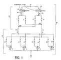
- FIG. 1is a schematic of a circuit for generating fine delay stages in a DLL.
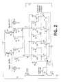
- FIG. 2is a schematic showing one embodiment of the circuit of FIG. 1 .
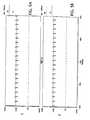
- FIG. 3Ais a graph of the relationship of input signals E and L (FIG. 2) to the circuit of FIG. 2 .
- FIG. 3Bis a graph of the relationship of input signals bE and bL (FIG. 2) to the circuit of FIG. 2 .
- FIG. 4Ais a graph of the phase relationship between input signal E and output signal OUT when signals S 0 -S 3 (FIG. 2) are low.
- FIG. 4Bis a graph of the phase relationship between the input signal E and the output signal OUT when signals S 0 -S 3 are high.
- FIG. 5Ais a graph of the relationship of I E and I L in FIG. 4 A.
- FIG. 5Bis a graph of the relationship of I E and I L in FIG. 4 B.
- FIGS. 6 a and 6 bare graphs of the relationship of I E and I L with respect to the phase delay between E and OUT.
- FIG. 7is a graph showing the relationship of the current switches of FIG. 1 to the generation of fine delay steps.
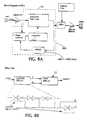
- FIG. 8Ais a general block diagram of a typical DLL
- FIG. 8Bis a general block diagram showing the usage of the fine delay circuit of FIG. 1 .
- Circuit 10contains an adjustable current source 15 that provides two output currents, I E and I L .
- Adjustable current source 15contains constant current sources 9 , 11 , 13 , and 17 , which produce currents I 1 , I 2 , I 3 , and I 4 , respectively, and current source switches 20 , 21 , 22 , 23 , 24 , 25 , 26 , and 27 .
- Switches 20 , 22 , 24 , and 26receive signals SO to S 3 .
- Switches 21 , 23 , 25 , 27receive signals bS 0 , bS 1 , bS 2 , and bS 3 , which are complementary to signals SO to S 3 . What is meant by complementary is that when one signal is high, its complementary signal is low, and vice versa.
- Circuit 10includes input switches 1 , 2 , 3 , and 4 .
- Input switch 1receives a first input clock signal E
- input switch 3receives a signal bE that is complementary to signal E
- input switch 2receives a second input clock signal L that is phase-shifted from signal E
- input switch 4receives a signal bL that complementary to signal L.
- the phase shift between signals E and Lis equal to one coarse delay T.
- Fine delay circuit 10produces an output voltage OUT that is phase-shifted from signal E.
- Coarse delay Tis defined as the difference of the minimum phase shift between signal E and signal OUT when current source signals to switches 20 , 22 , 24 , 26 are low (the switches are open) and the current source signals to 21 , 23 , 25 , and 27 are high (the switches are closed) and the maximum phase shift between signals E and OUT when current source signal 20 , 22 , 24 , 26 are high (the switches are closed) and current source signals to switches 21 , 23 , 25 , and 27 are low (the switches are open).
- constant current sources 9 , 11 , 13 , and 17include n-channel transistors 5 , 6 , 7 , and 8 respectively.
- the gate terminals of these transistorsare connected to a constant voltage potential, VC.
- the constant current sources I 1 , I 2 , I 3 , and I 4are binary weighted. That is, transistor 6 has twice the conductivity of transistor 5 , transistor 7 has twice the conductivity of transistor 6 , and transistor 8 has twice the conductivity of transistor 7 . In other words, if transistor 5 produces current I 1 , then transistor 6 produces a current 2 I 1 , transistor 7 produces a current 4 I 1 and transistor 8 produces a current, 8 I 1 . If additional transistors are added, the additional transistors would produce 2 N I 1 current, if desired.
- Each constant current sourceis connected to a pair of current sources switches.
- current source I 1connects to current source switches 20 and 21
- current source I 2connects to current source switches 22 and 23
- current source I 3connects to current source switches 24 and 25
- current source I 4connects to current source switches 26 and 27 .
- Each pair of switchesis comprised of two transistors.
- the gates of transistors 31 , 33 , 35 , and 37receive signals S 0 -S 3 and the gates of transistors 32 , 34 , 36 , and 38 receive the complementary signals bS 0 -bS 3 .
- the drain terminals of the constant current source transistors 5 , 6 , 7 , and 8connect to the current source switch at the source of the of n-channel transistors 31 , 32 , 33 , 34 , 35 , 36 , 37 , and 38 . That is, transistor 5 connects to transistor 31 and transistor 32 , transistor 6 connects to transistor 33 and transistor 34 , transistor 7 connects to transistor 35 and transistor 36 , and transistor 8 connects to transistor 37 and transistor 38 .
- FIGS. 3A and 3Bshow the relationship of signals E, L, bL, and bE in Circuit 10 .
- I Eis the sum of the current that passes through the input switches 1 and 2 .
- Input switches 1 and 2are comprised of two n-channel transistors 41 and 43 in FIG. 2 .
- the gate of transistor 41receives the input signal E and the gate of transistor 43 receives the input signal bE, which is the complement of signal E.
- the source of transistors 41 and 43are connected to the drain of the n-channel transistors 32 , 34 , 36 , and 38 .
- I Lis the sum of the current that passes through input switches 3 and 4 .
- Input switches 3 and 4are comprised of two n-channel transistors, 42 and 44 in FIG. 2 .
- the gate of transistor 42receives the input signal L and the gate of transistor 44 receives the input signal bL, which is the complement of signal L.
- the sources of transistors 42 and 44are connected to the drains of n-channel transistors 31 , 33 , 35 , and 37 .
- the drain terminals of transistor 41 and transistor 42are connected to a load 61 .
- the drain terminals of transistor 43 and transistor 44are connected to a load 62 .
- Load 61 and load 62are of equal resistance in this embodiment.
- the current through each of the loadsis equal to I LOAD .
- Output signal OUTis measured at a node 19 between load 62 and transistors 43 and 44 (FIG. 2 ).
- Node 19has a capacitor 52 connected to ground.
- a complement to output signal OUT, namely output signal OUTB,is measured at a node 18 between load 61 and transistors 41 and 42 .
- Node 18has a capacitor 51 connected to ground.
- the charging and discharging of capacitor 51 and capacitor 52is used by fine delay circuit 10 to create fine delay steps. The proper selection of capacitor 51 and capacitor 52 is made to allow for charging and discharging of the capacitors at high frequencies.
- the phase shift between signal E and OUTis adjusted in fine steps by current source switches 20 , 21 , 22 , 23 , 24 , 25 , 26 , and 27 .
- switch signals S 0 -S 3are at a minimum voltage designated as “0000”
- complementary signals bS 0 -bS 3are at a maximum voltage designated as “1111”.
- FIG. 7shows four stages of the sixteen stages.
- I L0.
- signal bEgoes low at tRE
- node 19is pulled-up through the resistor load resulting in Rise 1 having the fastest edge of the sixteen stages. Even if the signal bL goes low after a delay of one course delay, it will not affect node 19 because current I L is zero.
- Fall 1when bE goes high at tFE, node 19 discharges. Since all the current is in I E the discharge is the fastest of the sixteen stages.
- the functionis the same as Rise 2 except that the values of the currents I E and I L are different which slows the rate of charging.
- Fall 3functions the same as Fall 2 except that the change in current slows the rate of discharging.
- the charging of node 19begins only when signal bL goes low at tRL, which is the slowest rising edge of the sixteen stages.
- the node 19discharges only when bL goes high at tFL, which is the slowest falling edge of the sixteen falling edges.
- FIG. 7also shows the signal OUT 2 , which is the output voltage of an inverter connected to node 19 .
- the signal OUT(signal at node 19 ) crosses the voltage level VINV at different points in time according to the switch settings.
- VINVis the input threshold voltage of the inverter when the output of the inverter switches.
- FIG. 8Ashows a block diagram of the typical DLL 40 in a circuit.
- FIG. 8Bshows fine delay circuit 10 incorporated into a DLL block in which an input clock signal CLKIN produces a phase-shifted output clock signal CLKOUT.
- a fine stepis equal to 2 N and where N equals the number of binary weighted constant current sources.
- p-channel transistorscan be substituted for the n-channel transistors shown in the figures.
Landscapes
- Physics & Mathematics (AREA)
- Nonlinear Science (AREA)
- Pulse Circuits (AREA)
Abstract
Description
Claims (22)
Priority Applications (2)
| Application Number | Priority Date | Filing Date | Title |
|---|---|---|---|
| US09/871,855US6472921B1 (en) | 2001-05-31 | 2001-05-31 | Delivering a fine delay stage for a delay locked loop |
| DE10224218.6ADE10224218B4 (en) | 2001-05-31 | 2002-05-31 | Providing a fine delay stage for a delay locked loop |
Applications Claiming Priority (1)
| Application Number | Priority Date | Filing Date | Title |
|---|---|---|---|
| US09/871,855US6472921B1 (en) | 2001-05-31 | 2001-05-31 | Delivering a fine delay stage for a delay locked loop |
Publications (1)
| Publication Number | Publication Date |
|---|---|
| US6472921B1true US6472921B1 (en) | 2002-10-29 |
Family
ID=25358299
Family Applications (1)
| Application Number | Title | Priority Date | Filing Date |
|---|---|---|---|
| US09/871,855Expired - LifetimeUS6472921B1 (en) | 2001-05-31 | 2001-05-31 | Delivering a fine delay stage for a delay locked loop |
Country Status (2)
| Country | Link |
|---|---|
| US (1) | US6472921B1 (en) |
| DE (1) | DE10224218B4 (en) |
Cited By (7)
| Publication number | Priority date | Publication date | Assignee | Title |
|---|---|---|---|---|
| US6812760B1 (en) | 2003-07-02 | 2004-11-02 | Micron Technology, Inc. | System and method for comparison and compensation of delay variations between fine delay and coarse delay circuits |
| US20050068076A1 (en)* | 2003-09-26 | 2005-03-31 | Echere Iroaga | Current mirror compensation circuit and method |
| US20050068072A1 (en)* | 2003-09-26 | 2005-03-31 | Cosmin Iorga | Current mirror compensation using channel length modulation |
| US20060017478A1 (en)* | 2004-07-20 | 2006-01-26 | Micron Technology, Inc. | Delay-locked loop with feedback compensation |
| US20060208784A1 (en)* | 2005-03-17 | 2006-09-21 | Fujitsu Limited | Circuit for controlling phase with improved linearity of phase change |
| US20080042716A1 (en)* | 2006-06-27 | 2008-02-21 | Hynix Semiconductor Inc. | Delay apparatus of synchronizing circuit having improved jitter characteristic and method of controlling the same |
| US9584105B1 (en) | 2016-03-10 | 2017-02-28 | Analog Devices, Inc. | Timing generator for generating high resolution pulses having arbitrary widths |
Families Citing this family (1)
| Publication number | Priority date | Publication date | Assignee | Title |
|---|---|---|---|---|
| US7545194B2 (en)* | 2006-06-30 | 2009-06-09 | Intel Corporation | Programmable delay for clock phase error correction |
Citations (6)
| Publication number | Priority date | Publication date | Assignee | Title |
|---|---|---|---|---|
| US4118741A (en)* | 1976-02-18 | 1978-10-03 | Tokyo Shibaura Electric Co., Ltd. | Hue adjusting circuits |
| US4128817A (en)* | 1976-03-03 | 1978-12-05 | Tokyo Shibaura Electric Co., Ltd. | Voltage controlled oscillator with phase control circuits |
| US5015872A (en)* | 1988-07-06 | 1991-05-14 | Ant Nachrichtentechnik Gmbh | Method and circuit arrangement for generating a phase shifted clock pulse signal |
| US5489869A (en)* | 1994-05-17 | 1996-02-06 | Rockwell International | Antenna control unit attenuator and Bi-phase modulator |
| US6285228B1 (en)* | 1999-06-29 | 2001-09-04 | Infineon Technologies Ag | Integrated circuit for generating a phase-shifted output clock signal from a clock signal |
| US6385265B1 (en)* | 1998-08-04 | 2002-05-07 | Cypress Semiconductor Corp. | Differential charge pump |
Family Cites Families (2)
| Publication number | Priority date | Publication date | Assignee | Title |
|---|---|---|---|---|
| FR2690022B1 (en) | 1992-03-24 | 1997-07-11 | Bull Sa | VARIABLE DELAY CIRCUIT. |
| US6125157A (en) | 1997-02-06 | 2000-09-26 | Rambus, Inc. | Delay-locked loop circuitry for clock delay adjustment |
- 2001
- 2001-05-31USUS09/871,855patent/US6472921B1/ennot_activeExpired - Lifetime
- 2002
- 2002-05-31DEDE10224218.6Apatent/DE10224218B4/ennot_activeExpired - Fee Related
Patent Citations (6)
| Publication number | Priority date | Publication date | Assignee | Title |
|---|---|---|---|---|
| US4118741A (en)* | 1976-02-18 | 1978-10-03 | Tokyo Shibaura Electric Co., Ltd. | Hue adjusting circuits |
| US4128817A (en)* | 1976-03-03 | 1978-12-05 | Tokyo Shibaura Electric Co., Ltd. | Voltage controlled oscillator with phase control circuits |
| US5015872A (en)* | 1988-07-06 | 1991-05-14 | Ant Nachrichtentechnik Gmbh | Method and circuit arrangement for generating a phase shifted clock pulse signal |
| US5489869A (en)* | 1994-05-17 | 1996-02-06 | Rockwell International | Antenna control unit attenuator and Bi-phase modulator |
| US6385265B1 (en)* | 1998-08-04 | 2002-05-07 | Cypress Semiconductor Corp. | Differential charge pump |
| US6285228B1 (en)* | 1999-06-29 | 2001-09-04 | Infineon Technologies Ag | Integrated circuit for generating a phase-shifted output clock signal from a clock signal |
Cited By (15)
| Publication number | Priority date | Publication date | Assignee | Title |
|---|---|---|---|---|
| US6812760B1 (en) | 2003-07-02 | 2004-11-02 | Micron Technology, Inc. | System and method for comparison and compensation of delay variations between fine delay and coarse delay circuits |
| US20050030075A1 (en)* | 2003-07-02 | 2005-02-10 | Kim Kang Yong | System and method for comparison and compensation of delay variations between fine delay and coarse delay circuits |
| US7038511B2 (en) | 2003-07-02 | 2006-05-02 | Micron Technology, Inc. | System and method for comparison and compensation of delay variations between fine delay and coarse delay circuits |
| US20050068072A1 (en)* | 2003-09-26 | 2005-03-31 | Cosmin Iorga | Current mirror compensation using channel length modulation |
| WO2005031975A1 (en)* | 2003-09-26 | 2005-04-07 | Teradyne, Inc. | Timing generator with bias current compensation circuit and method |
| US20050068076A1 (en)* | 2003-09-26 | 2005-03-31 | Echere Iroaga | Current mirror compensation circuit and method |
| US7061307B2 (en) | 2003-09-26 | 2006-06-13 | Teradyne, Inc. | Current mirror compensation circuit and method |
| US7123075B2 (en) | 2003-09-26 | 2006-10-17 | Teradyne, Inc. | Current mirror compensation using channel length modulation |
| US20060017478A1 (en)* | 2004-07-20 | 2006-01-26 | Micron Technology, Inc. | Delay-locked loop with feedback compensation |
| US7078950B2 (en) | 2004-07-20 | 2006-07-18 | Micron Technology, Inc. | Delay-locked loop with feedback compensation |
| US20060208784A1 (en)* | 2005-03-17 | 2006-09-21 | Fujitsu Limited | Circuit for controlling phase with improved linearity of phase change |
| US7301383B2 (en)* | 2005-03-17 | 2007-11-27 | Fujitsu Limited | Circuit for controlling phase with improved linearity of phase change |
| US20080042716A1 (en)* | 2006-06-27 | 2008-02-21 | Hynix Semiconductor Inc. | Delay apparatus of synchronizing circuit having improved jitter characteristic and method of controlling the same |
| US7541854B2 (en)* | 2006-06-27 | 2009-06-02 | Hynix Semiconductor Inc. | Delay apparatus of synchronizing circuit having improved jitter characteristic and method of controlling the same |
| US9584105B1 (en) | 2016-03-10 | 2017-02-28 | Analog Devices, Inc. | Timing generator for generating high resolution pulses having arbitrary widths |
Also Published As
| Publication number | Publication date |
|---|---|
| DE10224218A1 (en) | 2003-02-06 |
| DE10224218B4 (en) | 2018-04-05 |
Similar Documents
| Publication | Publication Date | Title |
|---|---|---|
| US6356158B1 (en) | Phase-locked loop employing programmable tapped-delay-line oscillator | |
| KR100817962B1 (en) | Delayed locked loop phase blender circuit | |
| US6380783B1 (en) | Cyclic phase signal generation from a single clock source using current phase interpolation | |
| US6320437B1 (en) | Duty cycle regulator | |
| US7724051B2 (en) | DLL circuit, semiconductor device using the same, and method for controlling DLL circuit | |
| US6831493B2 (en) | Duty cycle regulator | |
| US6424193B1 (en) | Circuit for synchronizing frequencies of clock signals | |
| US8947141B2 (en) | Differential amplifiers, clock generator circuits, delay lines and methods | |
| KR100861919B1 (en) | Multiphase signal generator and its method | |
| KR100429127B1 (en) | Synchronous device | |
| JPH02141123A (en) | Digital delay element | |
| US6346839B1 (en) | Low power consumption integrated circuit delay locked loop and method for controlling the same | |
| US6329854B1 (en) | Phase locked loop integrated circuits having dynamic phase locking characteristics and methods of operating same | |
| JP5719333B2 (en) | Phase shift processing in delay locked loop / phase locked loop | |
| US6657468B1 (en) | Apparatus and method for controlling edge rates of digital signals | |
| US20020075050A1 (en) | Duty cycle regulator | |
| US5666088A (en) | Wide frequency range VCO with low jitter | |
| JPH10327055A (en) | Delay locked circuit | |
| US6472921B1 (en) | Delivering a fine delay stage for a delay locked loop | |
| US6559699B2 (en) | Dual control analog delay element | |
| US10367494B2 (en) | Fast-response references-less frequency detector | |
| US7113014B1 (en) | Pulse width modulator | |
| US6232813B1 (en) | Phase locked loop integrated circuits having fuse-enabled and fuse-disabled delay devices therein | |
| US11063597B1 (en) | Wide frequency range step size programmability for delay-locked loops using variable bias voltage generation | |
| US20030034816A1 (en) | Delay-locked loop for differential clock signals |
Legal Events
| Date | Code | Title | Description |
|---|---|---|---|
| AS | Assignment | Owner name:SIEMENS AG, GERMANY Free format text:ASSIGNMENT OF ASSIGNORS INTEREST;ASSIGNORS:RAO, RAJASHEKHAR;HEYNE, PATRICK;REEL/FRAME:012216/0871;SIGNING DATES FROM 20010701 TO 20010702 | |
| AS | Assignment | Owner name:INFINEON TECHNOLOGIES AKTIENGESELLSCHAFT, GERMANY Free format text:ASSIGNMENT OF ASSIGNORS INTEREST;ASSIGNOR:INFINEON TECHNOLOGIES AKTIENGESELLSCHAFT;REEL/FRAME:013147/0438 Effective date:20020722 | |
| STCF | Information on status: patent grant | Free format text:PATENTED CASE | |
| AS | Assignment | Owner name:INFINEON TECHNOLOGIES AKTIENGESELLSCHAFT, GERMANY Free format text:ASSIGNMENT OF ASSIGNORS INTEREST;ASSIGNOR:SIEMENS AKTIENGESELLSCHAFT;REEL/FRAME:017275/0198 Effective date:20020722 | |
| FPAY | Fee payment | Year of fee payment:4 | |
| AS | Assignment | Owner name:QIMONDA AG, GERMANY Free format text:ASSIGNMENT OF ASSIGNORS INTEREST;ASSIGNOR:INFINEON TECHNOLOGIES AG;REEL/FRAME:023773/0457 Effective date:20060425 | |
| FPAY | Fee payment | Year of fee payment:8 | |
| FPAY | Fee payment | Year of fee payment:12 | |
| AS | Assignment | Owner name:INFINEON TECHNOLOGIES AG, GERMANY Free format text:ASSIGNMENT OF ASSIGNORS INTEREST;ASSIGNOR:QIMONDA AG;REEL/FRAME:035623/0001 Effective date:20141009 | |
| AS | Assignment | Owner name:POLARIS INNOVATIONS LIMITED, IRELAND Free format text:ASSIGNMENT OF ASSIGNORS INTEREST;ASSIGNOR:INFINEON TECHNOLOGIES AG;REEL/FRAME:036808/0284 Effective date:20150708 |