US6472737B1 - Lead frame decoupling capacitor, semiconductor device packages including the same and methods - Google Patents
Lead frame decoupling capacitor, semiconductor device packages including the same and methodsDownload PDFInfo
- Publication number
- US6472737B1 US6472737B1US09/335,855US33585599AUS6472737B1US 6472737 B1US6472737 B1US 6472737B1US 33585599 AUS33585599 AUS 33585599AUS 6472737 B1US6472737 B1US 6472737B1
- Authority
- US
- United States
- Prior art keywords
- lead frame
- semiconductor device
- lead
- bus
- leads
- Prior art date
- Legal status (The legal status is an assumption and is not a legal conclusion. Google has not performed a legal analysis and makes no representation as to the accuracy of the status listed.)
- Expired - Lifetime
Links
Images


Classifications
- H—ELECTRICITY
- H01—ELECTRIC ELEMENTS
- H01L—SEMICONDUCTOR DEVICES NOT COVERED BY CLASS H10
- H01L23/00—Details of semiconductor or other solid state devices
- H01L23/48—Arrangements for conducting electric current to or from the solid state body in operation, e.g. leads, terminal arrangements ; Selection of materials therefor
- H01L23/488—Arrangements for conducting electric current to or from the solid state body in operation, e.g. leads, terminal arrangements ; Selection of materials therefor consisting of soldered or bonded constructions
- H01L23/495—Lead-frames or other flat leads
- H01L23/49589—Capacitor integral with or on the leadframe
- H—ELECTRICITY
- H01—ELECTRIC ELEMENTS
- H01L—SEMICONDUCTOR DEVICES NOT COVERED BY CLASS H10
- H01L24/00—Arrangements for connecting or disconnecting semiconductor or solid-state bodies; Methods or apparatus related thereto
- H01L24/01—Means for bonding being attached to, or being formed on, the surface to be connected, e.g. chip-to-package, die-attach, "first-level" interconnects; Manufacturing methods related thereto
- H01L24/42—Wire connectors; Manufacturing methods related thereto
- H01L24/47—Structure, shape, material or disposition of the wire connectors after the connecting process
- H01L24/49—Structure, shape, material or disposition of the wire connectors after the connecting process of a plurality of wire connectors
- H—ELECTRICITY
- H01—ELECTRIC ELEMENTS
- H01L—SEMICONDUCTOR DEVICES NOT COVERED BY CLASS H10
- H01L2224/00—Indexing scheme for arrangements for connecting or disconnecting semiconductor or solid-state bodies and methods related thereto as covered by H01L24/00
- H01L2224/01—Means for bonding being attached to, or being formed on, the surface to be connected, e.g. chip-to-package, die-attach, "first-level" interconnects; Manufacturing methods related thereto
- H01L2224/02—Bonding areas; Manufacturing methods related thereto
- H01L2224/04—Structure, shape, material or disposition of the bonding areas prior to the connecting process
- H01L2224/05—Structure, shape, material or disposition of the bonding areas prior to the connecting process of an individual bonding area
- H01L2224/0554—External layer
- H01L2224/0555—Shape
- H01L2224/05552—Shape in top view
- H01L2224/05554—Shape in top view being square
- H—ELECTRICITY
- H01—ELECTRIC ELEMENTS
- H01L—SEMICONDUCTOR DEVICES NOT COVERED BY CLASS H10
- H01L2224/00—Indexing scheme for arrangements for connecting or disconnecting semiconductor or solid-state bodies and methods related thereto as covered by H01L24/00
- H01L2224/01—Means for bonding being attached to, or being formed on, the surface to be connected, e.g. chip-to-package, die-attach, "first-level" interconnects; Manufacturing methods related thereto
- H01L2224/26—Layer connectors, e.g. plate connectors, solder or adhesive layers; Manufacturing methods related thereto
- H01L2224/31—Structure, shape, material or disposition of the layer connectors after the connecting process
- H01L2224/32—Structure, shape, material or disposition of the layer connectors after the connecting process of an individual layer connector
- H01L2224/321—Disposition
- H01L2224/32135—Disposition the layer connector connecting between different semiconductor or solid-state bodies, i.e. chip-to-chip
- H01L2224/32145—Disposition the layer connector connecting between different semiconductor or solid-state bodies, i.e. chip-to-chip the bodies being stacked
- H—ELECTRICITY
- H01—ELECTRIC ELEMENTS
- H01L—SEMICONDUCTOR DEVICES NOT COVERED BY CLASS H10
- H01L2224/00—Indexing scheme for arrangements for connecting or disconnecting semiconductor or solid-state bodies and methods related thereto as covered by H01L24/00
- H01L2224/01—Means for bonding being attached to, or being formed on, the surface to be connected, e.g. chip-to-package, die-attach, "first-level" interconnects; Manufacturing methods related thereto
- H01L2224/42—Wire connectors; Manufacturing methods related thereto
- H01L2224/47—Structure, shape, material or disposition of the wire connectors after the connecting process
- H01L2224/48—Structure, shape, material or disposition of the wire connectors after the connecting process of an individual wire connector
- H01L2224/4805—Shape
- H01L2224/4809—Loop shape
- H01L2224/48091—Arched
- H—ELECTRICITY
- H01—ELECTRIC ELEMENTS
- H01L—SEMICONDUCTOR DEVICES NOT COVERED BY CLASS H10
- H01L2224/00—Indexing scheme for arrangements for connecting or disconnecting semiconductor or solid-state bodies and methods related thereto as covered by H01L24/00
- H01L2224/01—Means for bonding being attached to, or being formed on, the surface to be connected, e.g. chip-to-package, die-attach, "first-level" interconnects; Manufacturing methods related thereto
- H01L2224/42—Wire connectors; Manufacturing methods related thereto
- H01L2224/47—Structure, shape, material or disposition of the wire connectors after the connecting process
- H01L2224/48—Structure, shape, material or disposition of the wire connectors after the connecting process of an individual wire connector
- H01L2224/4805—Shape
- H01L2224/4809—Loop shape
- H01L2224/48095—Kinked
- H—ELECTRICITY
- H01—ELECTRIC ELEMENTS
- H01L—SEMICONDUCTOR DEVICES NOT COVERED BY CLASS H10
- H01L2224/00—Indexing scheme for arrangements for connecting or disconnecting semiconductor or solid-state bodies and methods related thereto as covered by H01L24/00
- H01L2224/01—Means for bonding being attached to, or being formed on, the surface to be connected, e.g. chip-to-package, die-attach, "first-level" interconnects; Manufacturing methods related thereto
- H01L2224/42—Wire connectors; Manufacturing methods related thereto
- H01L2224/47—Structure, shape, material or disposition of the wire connectors after the connecting process
- H01L2224/48—Structure, shape, material or disposition of the wire connectors after the connecting process of an individual wire connector
- H01L2224/481—Disposition
- H01L2224/48151—Connecting between a semiconductor or solid-state body and an item not being a semiconductor or solid-state body, e.g. chip-to-substrate, chip-to-passive
- H01L2224/48221—Connecting between a semiconductor or solid-state body and an item not being a semiconductor or solid-state body, e.g. chip-to-substrate, chip-to-passive the body and the item being stacked
- H01L2224/48245—Connecting between a semiconductor or solid-state body and an item not being a semiconductor or solid-state body, e.g. chip-to-substrate, chip-to-passive the body and the item being stacked the item being metallic
- H01L2224/48247—Connecting between a semiconductor or solid-state body and an item not being a semiconductor or solid-state body, e.g. chip-to-substrate, chip-to-passive the body and the item being stacked the item being metallic connecting the wire to a bond pad of the item
- H—ELECTRICITY
- H01—ELECTRIC ELEMENTS
- H01L—SEMICONDUCTOR DEVICES NOT COVERED BY CLASS H10
- H01L2224/00—Indexing scheme for arrangements for connecting or disconnecting semiconductor or solid-state bodies and methods related thereto as covered by H01L24/00
- H01L2224/01—Means for bonding being attached to, or being formed on, the surface to be connected, e.g. chip-to-package, die-attach, "first-level" interconnects; Manufacturing methods related thereto
- H01L2224/42—Wire connectors; Manufacturing methods related thereto
- H01L2224/47—Structure, shape, material or disposition of the wire connectors after the connecting process
- H01L2224/48—Structure, shape, material or disposition of the wire connectors after the connecting process of an individual wire connector
- H01L2224/481—Disposition
- H01L2224/48151—Connecting between a semiconductor or solid-state body and an item not being a semiconductor or solid-state body, e.g. chip-to-substrate, chip-to-passive
- H01L2224/48221—Connecting between a semiconductor or solid-state body and an item not being a semiconductor or solid-state body, e.g. chip-to-substrate, chip-to-passive the body and the item being stacked
- H01L2224/48245—Connecting between a semiconductor or solid-state body and an item not being a semiconductor or solid-state body, e.g. chip-to-substrate, chip-to-passive the body and the item being stacked the item being metallic
- H01L2224/48257—Connecting between a semiconductor or solid-state body and an item not being a semiconductor or solid-state body, e.g. chip-to-substrate, chip-to-passive the body and the item being stacked the item being metallic connecting the wire to a die pad of the item
- H—ELECTRICITY
- H01—ELECTRIC ELEMENTS
- H01L—SEMICONDUCTOR DEVICES NOT COVERED BY CLASS H10
- H01L2224/00—Indexing scheme for arrangements for connecting or disconnecting semiconductor or solid-state bodies and methods related thereto as covered by H01L24/00
- H01L2224/01—Means for bonding being attached to, or being formed on, the surface to be connected, e.g. chip-to-package, die-attach, "first-level" interconnects; Manufacturing methods related thereto
- H01L2224/42—Wire connectors; Manufacturing methods related thereto
- H01L2224/47—Structure, shape, material or disposition of the wire connectors after the connecting process
- H01L2224/49—Structure, shape, material or disposition of the wire connectors after the connecting process of a plurality of wire connectors
- H01L2224/491—Disposition
- H01L2224/4912—Layout
- H01L2224/49171—Fan-out arrangements
- H—ELECTRICITY
- H01—ELECTRIC ELEMENTS
- H01L—SEMICONDUCTOR DEVICES NOT COVERED BY CLASS H10
- H01L24/00—Arrangements for connecting or disconnecting semiconductor or solid-state bodies; Methods or apparatus related thereto
- H01L24/01—Means for bonding being attached to, or being formed on, the surface to be connected, e.g. chip-to-package, die-attach, "first-level" interconnects; Manufacturing methods related thereto
- H01L24/42—Wire connectors; Manufacturing methods related thereto
- H01L24/47—Structure, shape, material or disposition of the wire connectors after the connecting process
- H01L24/48—Structure, shape, material or disposition of the wire connectors after the connecting process of an individual wire connector
- H—ELECTRICITY
- H01—ELECTRIC ELEMENTS
- H01L—SEMICONDUCTOR DEVICES NOT COVERED BY CLASS H10
- H01L2924/00—Indexing scheme for arrangements or methods for connecting or disconnecting semiconductor or solid-state bodies as covered by H01L24/00
- H01L2924/0001—Technical content checked by a classifier
- H01L2924/00014—Technical content checked by a classifier the subject-matter covered by the group, the symbol of which is combined with the symbol of this group, being disclosed without further technical details
- H—ELECTRICITY
- H01—ELECTRIC ELEMENTS
- H01L—SEMICONDUCTOR DEVICES NOT COVERED BY CLASS H10
- H01L2924/00—Indexing scheme for arrangements or methods for connecting or disconnecting semiconductor or solid-state bodies as covered by H01L24/00
- H01L2924/01—Chemical elements
- H01L2924/01027—Cobalt [Co]
- H—ELECTRICITY
- H01—ELECTRIC ELEMENTS
- H01L—SEMICONDUCTOR DEVICES NOT COVERED BY CLASS H10
- H01L2924/00—Indexing scheme for arrangements or methods for connecting or disconnecting semiconductor or solid-state bodies as covered by H01L24/00
- H01L2924/01—Chemical elements
- H01L2924/01029—Copper [Cu]
- H—ELECTRICITY
- H01—ELECTRIC ELEMENTS
- H01L—SEMICONDUCTOR DEVICES NOT COVERED BY CLASS H10
- H01L2924/00—Indexing scheme for arrangements or methods for connecting or disconnecting semiconductor or solid-state bodies as covered by H01L24/00
- H01L2924/01—Chemical elements
- H01L2924/01076—Osmium [Os]
- H—ELECTRICITY
- H01—ELECTRIC ELEMENTS
- H01L—SEMICONDUCTOR DEVICES NOT COVERED BY CLASS H10
- H01L2924/00—Indexing scheme for arrangements or methods for connecting or disconnecting semiconductor or solid-state bodies as covered by H01L24/00
- H01L2924/01—Chemical elements
- H01L2924/01079—Gold [Au]
- H—ELECTRICITY
- H01—ELECTRIC ELEMENTS
- H01L—SEMICONDUCTOR DEVICES NOT COVERED BY CLASS H10
- H01L2924/00—Indexing scheme for arrangements or methods for connecting or disconnecting semiconductor or solid-state bodies as covered by H01L24/00
- H01L2924/10—Details of semiconductor or other solid state devices to be connected
- H01L2924/11—Device type
- H01L2924/14—Integrated circuits
- H01L2924/143—Digital devices
- H01L2924/1433—Application-specific integrated circuit [ASIC]
- H—ELECTRICITY
- H01—ELECTRIC ELEMENTS
- H01L—SEMICONDUCTOR DEVICES NOT COVERED BY CLASS H10
- H01L2924/00—Indexing scheme for arrangements or methods for connecting or disconnecting semiconductor or solid-state bodies as covered by H01L24/00
- H01L2924/15—Details of package parts other than the semiconductor or other solid state devices to be connected
- H01L2924/181—Encapsulation
- H—ELECTRICITY
- H01—ELECTRIC ELEMENTS
- H01L—SEMICONDUCTOR DEVICES NOT COVERED BY CLASS H10
- H01L2924/00—Indexing scheme for arrangements or methods for connecting or disconnecting semiconductor or solid-state bodies as covered by H01L24/00
- H01L2924/19—Details of hybrid assemblies other than the semiconductor or other solid state devices to be connected
- H01L2924/1901—Structure
- H01L2924/1904—Component type
- H01L2924/19041—Component type being a capacitor
- H—ELECTRICITY
- H01—ELECTRIC ELEMENTS
- H01L—SEMICONDUCTOR DEVICES NOT COVERED BY CLASS H10
- H01L2924/00—Indexing scheme for arrangements or methods for connecting or disconnecting semiconductor or solid-state bodies as covered by H01L24/00
- H01L2924/30—Technical effects
- H01L2924/301—Electrical effects
- H01L2924/30107—Inductance
- H—ELECTRICITY
- H01—ELECTRIC ELEMENTS
- H01L—SEMICONDUCTOR DEVICES NOT COVERED BY CLASS H10
- H01L2924/00—Indexing scheme for arrangements or methods for connecting or disconnecting semiconductor or solid-state bodies as covered by H01L24/00
- H01L2924/30—Technical effects
- H01L2924/301—Electrical effects
- H01L2924/3011—Impedance
- H—ELECTRICITY
- H01—ELECTRIC ELEMENTS
- H01L—SEMICONDUCTOR DEVICES NOT COVERED BY CLASS H10
- H01L2924/00—Indexing scheme for arrangements or methods for connecting or disconnecting semiconductor or solid-state bodies as covered by H01L24/00
- H01L2924/30—Technical effects
- H01L2924/301—Electrical effects
- H01L2924/3025—Electromagnetic shielding
Definitions
- the present inventionrelates to semiconductor device assemblies employing multi-layered lead frames and, more specifically, to semiconductor device assemblies disposing a decoupling capacitor in a close, substantially co-extensive relationship with a semiconductor device bearing an integrated circuit.
- the integrated circuits carried on a semiconductor devicewould ideally be electrically connected to conductive traces on carrier substrates such as printed circuit boards and thus to other semiconductor devices carried on the same or other such substrates by infinitesimally short conductors, eliminating impedance problems such as undesirable inductance and other conductor-induced system noise.
- DRAMsdynamic random access memories
- I/Osinputs and outputs
- lead inductance in IC packageshas not traditionally been troublesome because slow signal frequencies of past devices render such inductance relatively insignificant, faster and ever-increasing signal frequencies of state-of-the-art electronic systems have substantially increased the practical significance of lead inductance.
- performance of integrated circuit dice using lead frames for external electrical connectionis slower than desirable because the inductance associated with the lead fingers slows changes in signal currents through the leads, prolonging signal propagation through the leads.
- digital signals propagating along the lead fingersare dispersing or “spreading out” because the so-called “Fourier” components of various frequencies making up the digital signals propagate through the inductance associated with the lead fingers at different speeds, causing the signal components and thus the signals themselves to disperse along the lead fingers. While mild dispersion merely widens the digital signals without detrimental effect, severe dispersion can make the digital signals unrecognizable upon receipt.
- so-called “reflection” signals propagating along the lead fingers as a result of impedance mismatches between the lead fingers and associated semiconductor device or between the lead fingers and external circuitry, caused in part by lead-associated inductancecan distort normal signals propagating along the lead fingers concurrently with the reflection signals.
- LOClead-over-chip
- the semiconductor deviceis then supported from the undersides of the extending lead fingers, typically through an intervening polyimide film such as a KaptonTM tape having an adhesive coating on its upper and lower surfaces, the film serving as a dielectric, an alpha barrier and a protective coating for the active surface.
- an intervening polyimide filmsuch as a KaptonTM tape having an adhesive coating on its upper and lower surfaces, the film serving as a dielectric, an alpha barrier and a protective coating for the active surface.
- the LOC-type long, mutually parallel lead finger runs over the active surfacebecome abusive in terms of unacceptably increasing real impedance as well as lead inductance (both self and mutual) in the circuit.
- lead finger runsalso increase signal reflection in the circuit due to transmission line effects and degrade signal integrity due to the aforementioned propagation delays, switching noise, and crosstalk.
- elimination of the die-attach paddlealso eliminates the potential for employing a ground plane under the semiconductor device without additional processing steps, and such a ground plane in any case would not alleviate the problems attendant to use of the long lead fingers extending over the semiconductor device's active surface.
- LOC configurationsare merely one example of the type of packaging promoting the above-referenced undesirable noise phenomena.
- LOClead-under-chip
- Such configurationsinclude lead-under-chip (LUC) configurations, and configurations wherein a large number of leads extend from several sides of a semiconductor device to a single side or edge of a package, such as in a vertical surface mount package, or VSMP.
- U.S. Pat. No. 5,214,845assigned to the assignee of the present invention, employs a flexible, laminated sandwich assembly of an outer ground plane and an outer power plane dielectrically isolated from a series of conductive traces running therebetween.
- the traces and planesare connected to corresponding bond pads on the semiconductor device at one end, and to lead fingers on the other, as by thermocompression bonding (in the case of a TAB embodiment) or by wire bonds.
- thermocompression bondingin the case of a TAB embodiment
- wire bondswire bonds
- the inventorshave recognized the need for a low-cost, reduced-inductance circuit configuration adaptable to current packaging designs and employing conventional and readily-available materials, equipment and fabrication techniques.
- a semiconductor device package according to the present inventionincludes a substrate and a semiconductor device disposed upon the substrate.
- a multi-layer lead frame of the leads-over-chip (LOC) type, leads-under-chip (LUC) type, or other type of lead frame arrangementprovides an electrically conductive passageway from the semiconductor device disposed upon the substrate to devices that are external of the assembly.
- the multiple layers of the lead frameare joined by an interposed dielectric layer, which is also referred to as an insulator element, and each include a wide, electrically conductive bus.
- the layersmay form a “paddle” or “support platform” to which a semiconductor device is secured.
- the bus of one of the lead frame layersis a power supply bus, while the bus of the other lead frame layer is a ground bus.
- the buses of each layerat least partially overlap to form a decoupling capacitor over a portion of the semiconductor device.
- One of the lead frame layersincludes a wide bus having one or more ground (V SS ) lead fingers electrically connected thereto.
- Another of the lead frame layersincludes a wide bus having one or more power (V CC ) lead fingers electrically connected thereto.
- the decoupling capacitorreduces coupling and suppresses noise that is typically produced by the power supply components. Moreover, the juxtaposition and placement of the power supply lead fingers adjacent the sides of the semiconductor device package and away from (i.e., not interleaved with) the remaining lead fingers reduces the troublesome characteristics of mutual inductance and self inductance. Further, the placement of the buses in positions that would otherwise be occupied by long, adjacent, bent lead fingers also eliminates the magnetic fields that are typically generated by such lead fingers.
- the multi-layer lead frame of the present inventionalso imparts at least a nominal heat sink effect to the semiconductor device, promoting the more even distribution of heat that is generated during operation of the semiconductor device than might be achieved through the lead fingers alone.
- This heat sink effectmay be enhanced by increasing the mass of one or more of the lead frame buses, as by enhancing their thickness within the constraints of the package dimensions, or by configuring the buses with one or more portions extending to the exterior of the package. While this latter approach may render the device more susceptible to external radio-frequency interference, such an arrangement may be shielded, if necessary, by techniques known in the art. Such variation is especially useful in embodiments of the present invention wherein the semiconductor device is enclosed in a plastic, ceramic, or other type of package.
- the device to be fabricatedcomprise a leads-over-chip device
- conventional polyimide or other dielectric film or tape stripsmay be adhered to one side of the lead fingers, and the semiconductor devices subsequently adhered to the film by their active surfaces as known in the art prior to electrical connection of the semiconductor device and lead frames.
- multi-layered lead frame according to the present inventionmay be employed for an enhancement to any conventional plastic package design having adequate depth between the planes in which the lead fingers are positioned and the exterior surface of the package.
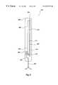
- FIG. 1is a top plan view of a vertical surface mount package (VSMP)-configured semiconductor device and multi-layered lead frame assembly secured together such that the lead frame overlaps the active surface of the semiconductor device, and employing a decoupling capacitor according to the present invention;
- VSMPvertical surface mount package
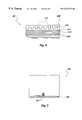
- FIG. 2is an enlarged side plan view of the assembly of FIG. 1;
- FIG. 3is an enlarged side plan view illustrating a vertical surface mount package-configured semiconductor device and lead frame assembly secured together such that the lead frame overlaps the back side of the semiconductor device, and employing a decoupling capacitor according to the present invention
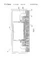
- FIG. 4is a top plan view of a packaged embodiment of the assembly of the present invention, depicting an alternative decoupling capacitor wherein at least one of the capacitor plates extends to the periphery of the package to provide enhanced heat transfer and distribution capabilities;
- FIG. 5is an enlarged side plan view of a portion of a leads-over-chip (LOC)-configured semiconductor device and lead frame assembly as depicted in FIG. 4, but employing at least one capacitor plate modified to provide enhanced heat transfer and distribution capabilities;
- LOCleads-over-chip
- FIG. 6is a top plan view of the assembly in FIG. 1, depicting alternatively shaped lead frame layers;
- FIG. 7is a schematic representation of the semiconductor device assembly according to the present invention associated with an electronic system.
- a semiconductor device assembly 20 of the present inventionis shown which includes a semiconductor device 100 , also termed an integrated circuit die, that is mounted to a lead frame 102 and upon a substrate 108 in a vertical surface mount package (VSMP) configuration.
- VSMPvertical surface mount package
- An outline of the outer periphery of substrate 108is shown at line 110 .
- Lead frame 102includes a plurality of lead fingers 104 , 105 A, 105 B, each of which are configured to extend across the outer periphery of substrate 108 along a single side or edge 106 thereof for external connection.
- Substrate 108preferably comprises any suitable, well-known substrate material for use with a semiconductor device.
- Semiconductor device 100may be secured to a major surface of substrate 108 by any suitable means, such as adhesive attachment.
- lead frame 102includes a first layer 102 A and a second layer 102 B and performs as a die attach paddle, to which the active surface 122 of semiconductor device 100 is secured.
- Lead frame 102may be secured to substrate 108 so that first bus 112 overlaps semiconductor device 100 and so the lead frame is oriented relative to the semiconductor device in either a lead-over-chip (LOC) configuration or so the lead fingers 104 , 105 thereof terminate proximate to the periphery of the semiconductor device, without overlapping the same.
- lead frame 102may be secured to substrate 108 , and the back side of semiconductor device 100 disposed over the lead frame, such as in a leads-under-chip configuration or otherwise.
- Lead fingers 104may also be attached to substrate 108 .
- the securing material 111which secures semiconductor device 100 and/or lead frame 102 to substrate 108 , is preferably a good thermal conductor to facilitate the distribution and dissipation of heat from semiconductor device 100 to lead frame 102 and/or substrate 108 .
- Securing material 111may comprise any suitable well-known type of electrically insulative film that may be adhesively coated to secure semiconductor device 100 and lead frame 102 to substrate 108 , such as the polyimide film having adhesive on both surfaces thereof that is sold under the trade name KAPTONTM by E.I. du Pont de Nemours & Company of Wilmington, Del.
- the first layer 102 A of lead frame 102includes an electrically conductive, wide first bus 112 that extends over a portion of the surface of semiconductor device 100 and a first plurality of lead fingers 105 that extend in substantially the same direction. Lead fingers 105 of first layer 102 A extend from or are otherwise electrically connected with first bus 112 .
- Second layer 102 Bincludes an electrically conductive, wide second bus 114 that also extends over a portion of the surface of semiconductor device 100 and a second plurality of lead fingers 104 that extend therefrom in substantially the same direction. Some of lead fingers 104 extend from or are otherwise electrically connected with second bus 114 .
- First bus 112 and second bus 114are oriented in such a manner that a substantial portion of the area of each of first bus 112 and second bus 114 overlap.
- First bus 112 and second bus 114each preferably comprise a low resistivity, high conductivity sheet of material such as copper or gold, although copper is preferred from a cost standpoint.
- An insulating element 148(FIG. 2) is disposed between first layer 102 A and second layer 102 B to adhere the first and second lead frame layers together and to separate the overlapping portions of first bus 112 and second bus 114 .
- Insulating element 148is preferably manufactured from a dielectric or insulating material such as a polyimide film carrying adhesive on both surfaces thereof. An example of such a film is that sold under the trade name KAPTONTM by du Pont.
- Bond wires 124establish electrical connections between bond pads 120 on the active surface 122 of semiconductor device 100 and the lead fingers 104 of lead frame 102 .
- bond wires 124facilitate the passage of signals between the integrated circuitry that is carried on active surface 122 of semiconductor device 100 and external circuitry (not shown), such as conductive traces on a carrier substrate (e.g., a printed circuit board), and other conductors and active and passive components packaged in the same or a higher level.
- device assemblieswhich employ direct thermocompression bonding of lead fingers 104 , 105 to bond pads 120 , flex-circuit-type connections between lead fingers 104 , 105 and bond pads 120 using conductors in a preformed pattern carried on a thin dielectric (typically termed tape automated bonding, or “TAB”, connections), or other known apparatus and processes may be employed for establishing electrical connections with the bond pads of a semiconductor device.
- TABtape automated bonding
- a central group 140 of lead fingers 104extends between a side 126 of semiconductor device 100 that lies closest to edge 106 of substrate 108 .
- Each of the lead fingers 104 of central group 140are extremely short, straight, mutually parallel, and of substantially uniform length.
- Adjacent each side of central group 140are flanking groups 141 and 142 of discrete lead fingers 104 .
- Each lead finger in flanking groups 141 and 142extends between transverse sides 128 and 130 of semiconductor device 100 and edge 106 and have various lengths.
- Most of the lead fingers 104 of flanking groups 141 and 142curve to form a 90 degree angle from their respective, substantially perpendicular orientation relative to transverse sides 128 , 130 to an orientation that is substantially perpendicular to edge 106 as they exit the latter.
- Flanking groups 141 and 142are each flanked by a group of lead fingers 105 B, which are electrically connected with and may be commonly connected to and extend from second bus 114 , and are referred to as second bus extension groups 143 and 144 , respectively.
- each of second bus extension groups 143 and 144are flanked by another group of lead fingers 105 A that are electrically connected with first bus 112 , and are referred to as first bus extension groups 145 and 146 , respectively.
- Lead fingers 105 Amay be commonly connected to first bus 112 and extend therefrom.
- first and second buses 112 or 114is electrically connected to a ground (V SS ) through its respective groups of lead fingers 105 while the other of the buses is electrically connected to a power supply source (V CC ), which is also referred to as a power source (V CC ), through its respective groups of lead fingers 105 .
- first bus 112 of first layer 102 A of lead frame 102may be electrically connected to a power source (V CC ) by its corresponding lead fingers 105 A (of first bus extension groups 145 and 146 ), and second bus 114 is electrically connected to a ground (V SS ) by its corresponding lead fingers 105 B (of second bus extension groups 143 and 144 ).
- lead fingers 105 A and 105 BBy commonly connecting lead fingers 105 A to each other and lead fingers 105 B to each other, as depicted, impedance is reduced, thereby facilitating the use of semiconductor devices 100 having high operating frequencies in semiconductor device assembly 20 . Additionally, the depicted arrangement imparts lead fingers 105 A and 105 B with impedance that is similar to that of lead fingers 104 .
- the ground and power supply bond pads 120 on semiconductor device 100are electrically connected (by bond wires 124 ) to the respective ground bus (second bus 114 in the embodiment illustrated in FIGS. 1 and 2) and power supply bus (first bus 112 in the embodiment illustrated in FIGS. 1 and 2 ).
- the shape and orientation of the first and second buses 112 and 114facilitate the use of very short bond wires 124 in order to reduce the conductor inductances between the decoupling capacitor and the bond pads 120 that are electrically connected therewith.
- First bus 112 and second bus 114act as capacitor plates and, in combination with insulating element 148 , create a decoupling capacitor 116 that extends over a portion of the surface of semiconductor device 100 .
- the orientation of V CC and V SS (i.e., of first bus 112 and second bus 114 ) relative to semiconductor device 100may be reversed, as may the positioning of the first and second bus extension groups 145 , 146 and 143 , 144 relative to flanking groups 141 and 142 .
- the power supply (V CC ) lead fingers 105 Ai.e., the lead fingers of groups 145 and 146
- the lead fingers 104 of central group 140 and flanking groups 141 and 142are separated from the lead fingers 104 of central group 140 and flanking groups 141 and 142 by grounded lead fingers 105 B (i.e., the lead fingers of groups 143 and 144 ).
- This arrangementreduces the incidence of magnetic couplng or mutual inductance that may be caused by a power supply lead finger that is ) adjacent to another lead finger.
- semiconductor device 100preferably comprises a 64 megabit vertical surface mount package-configured, seventy ( 70 ) lead dynamic random access memory (DRAM), although the invention is not limited to the package configuration shown and described, or to a dynamic random access memory or other memory devices (including without limitation static random access memories (SRAMs), synchronous dynamic random access memories (SDRAMs), sequential graphics random access memories (SGRAMs), electrically erasable programmable read-only memories (EEPROMs) and flash memories).
- SRAMsstatic random access memories
- SDRAMssynchronous dynamic random access memories
- SGRAMssequential graphics random access memories
- EEPROMselectrically erasable programmable read-only memories
- flash memorieselectrically erasable programmable read-only memories
- ASICsapplication-specific integrated circuits
- FIG. 3another embodiment of the semiconductor device assembly 20 ′ according to the present invention is shown wherein the multi-layered lead frame 202 , including a first bus 212 and a second bus 214 , is attached to the base 218 of semiconductor device 200 with a securing material 211 , such as that described above in reference to FIG. 1 .
- First bus 212 and second bus 214are separated by an insulating element 248 , such as that described above in reference to FIG. 1, in order to form a decoupling capacitor.
- Lead fingers 204which preferably extend substantially unidirectionally from semiconductor device assembly 20 ′, are electrically connected with bond pads 220 on the active surface 222 of semiconductor device 200 . This electrical connection may be established by bond wires 224 , or as otherwise known in the art.
- a so-called “plastic” package 208may be disposed over semiconductor device 200 and lead frame 202 .
- semiconductor device assembly 20may also comprise a so-called “plastic” package 109 ′ comprising a transfer-molded, filled polymer compound, as known in the art (FIGS. 1 and 2 also depict a package 109 ).
- plastic package 109 ′comprising a transfer-molded, filled polymer compound, as known in the art (FIGS. 1 and 2 also depict a package 109 ).
- alternative packagingsuch as preformed ceramic packages and potted encapsulants may also be used in the present invention.
- lead frame 102 ′may also include extensions 113 ′ of either first bus 112 ′, second bus 114 ′, or both of them which extend to the outer periphery of the semiconductor device package in order to facilitate the dissipation of heat from the same. While extensions 113 ′ may render the semiconductor device package more susceptible to external radio-frequency interference, such an arrangement may be shielded, if necessary, by techniques known in the art.
- the outermost (relative to the semiconductor device) bus 212 ′may be configured with additional mass in the form of fins or other projections 270 ′ opposite the underlying bus 214 ′ and the semiconductor device. Projections 270 ′ may extend to the exterior of package 209 ′, which surrounds semiconductor device 200 ′, as shown in broken lines 272 ′. Other mass increasing configurations are also possible and limited only by the available interior space of the package and the need to maintain the electrical performance of the packaged device.
- the heat sinks depicted in FIGS. 4 and 5may also be used in embodiments of the semiconductor device assembly that are not enclosed within a package.
- FIG. 6illustrates a variation of the lead frame layers 102 A and 102 B of semiconductor device package 20 , wherein the shape of the lead frame layers differs from that illustrated in FIGS. 1 and 4.
- the decoupling capacitor of the inventionprovides a modest improvement to electromagnetic interference (EMI) shielding.
- EMIelectromagnetic interference
- the busesshould extend over the semiconductor device in a manner which permits the wire-bonding capillary to form a wire bond over the desired bond pads. Additionally, the transverse distance or space between the buses should be minimized, in order to maximize the beneficial effects of the invention. Finally, the surface areas of the coextensive portions of the buses should be maximized, but a sufficient portion of the periphery of the buses should be contained within the material of the package surrounding the semiconductor device and lead frame combination, with enough space or clearance between the edges of the buses and the exterior of the package so that package integrity and reliability is not affected.
- FIG. 7is a schematic representation of an electronic system 700 , which includes a carrier substrate 702 .
- a semiconductor device assembly 20 according to the present inventionis in electrical communication with carrier substrate 702 .
- semiconductor device assembly 20is operatively associated with electronic system 700 .
Landscapes
- Engineering & Computer Science (AREA)
- Power Engineering (AREA)
- Computer Hardware Design (AREA)
- Microelectronics & Electronic Packaging (AREA)
- Physics & Mathematics (AREA)
- Condensed Matter Physics & Semiconductors (AREA)
- General Physics & Mathematics (AREA)
- Lead Frames For Integrated Circuits (AREA)
Abstract
Description
Claims (21)
Priority Applications (2)
| Application Number | Priority Date | Filing Date | Title |
|---|---|---|---|
| US09/335,855US6472737B1 (en) | 1998-01-20 | 1999-06-17 | Lead frame decoupling capacitor, semiconductor device packages including the same and methods |
| US10/230,819US6717257B2 (en) | 1998-01-20 | 2002-08-29 | Lead frame decoupling capacitor, semiconductor device packages including the same and methods |
Applications Claiming Priority (2)
| Application Number | Priority Date | Filing Date | Title |
|---|---|---|---|
| US09/009,668US6515359B1 (en) | 1998-01-20 | 1998-01-20 | Lead frame decoupling capacitor semiconductor device packages including the same and methods |
| US09/335,855US6472737B1 (en) | 1998-01-20 | 1999-06-17 | Lead frame decoupling capacitor, semiconductor device packages including the same and methods |
Related Parent Applications (1)
| Application Number | Title | Priority Date | Filing Date |
|---|---|---|---|
| US09/009,668DivisionUS6515359B1 (en) | 1998-01-20 | 1998-01-20 | Lead frame decoupling capacitor semiconductor device packages including the same and methods |
Related Child Applications (1)
| Application Number | Title | Priority Date | Filing Date |
|---|---|---|---|
| US10/230,819ContinuationUS6717257B2 (en) | 1998-01-20 | 2002-08-29 | Lead frame decoupling capacitor, semiconductor device packages including the same and methods |
Publications (1)
| Publication Number | Publication Date |
|---|---|
| US6472737B1true US6472737B1 (en) | 2002-10-29 |
Family
ID=21739035
Family Applications (5)
| Application Number | Title | Priority Date | Filing Date |
|---|---|---|---|
| US09/009,668Expired - LifetimeUS6515359B1 (en) | 1998-01-20 | 1998-01-20 | Lead frame decoupling capacitor semiconductor device packages including the same and methods |
| US09/335,855Expired - LifetimeUS6472737B1 (en) | 1998-01-20 | 1999-06-17 | Lead frame decoupling capacitor, semiconductor device packages including the same and methods |
| US10/230,819Expired - Fee RelatedUS6717257B2 (en) | 1998-01-20 | 2002-08-29 | Lead frame decoupling capacitor, semiconductor device packages including the same and methods |
| US10/269,191Expired - Fee RelatedUS7071542B2 (en) | 1998-01-20 | 2002-10-11 | Lead frame decoupling capacitor, semiconductor device packages including the same and methods |
| US11/326,078AbandonedUS20060118924A1 (en) | 1998-01-20 | 2006-01-05 | Lead frame assemblies and decoupling capacitors |
Family Applications Before (1)
| Application Number | Title | Priority Date | Filing Date |
|---|---|---|---|
| US09/009,668Expired - LifetimeUS6515359B1 (en) | 1998-01-20 | 1998-01-20 | Lead frame decoupling capacitor semiconductor device packages including the same and methods |
Family Applications After (3)
| Application Number | Title | Priority Date | Filing Date |
|---|---|---|---|
| US10/230,819Expired - Fee RelatedUS6717257B2 (en) | 1998-01-20 | 2002-08-29 | Lead frame decoupling capacitor, semiconductor device packages including the same and methods |
| US10/269,191Expired - Fee RelatedUS7071542B2 (en) | 1998-01-20 | 2002-10-11 | Lead frame decoupling capacitor, semiconductor device packages including the same and methods |
| US11/326,078AbandonedUS20060118924A1 (en) | 1998-01-20 | 2006-01-05 | Lead frame assemblies and decoupling capacitors |
Country Status (1)
| Country | Link |
|---|---|
| US (5) | US6515359B1 (en) |
Cited By (6)
| Publication number | Priority date | Publication date | Assignee | Title |
|---|---|---|---|---|
| US20060007632A1 (en)* | 2002-05-24 | 2006-01-12 | Koninklijke Philips Electronics N.V. | Decoupling module for decoupling high-frequency signals from a power supply line |
| EP1956653A1 (en) | 2007-02-06 | 2008-08-13 | Siemens Audiologische Technik GmbH | Switching device with bonded SMD component |
| US20090152694A1 (en)* | 2007-12-12 | 2009-06-18 | Infineon Technologies Ag | Electronic device |
| US20100007006A1 (en)* | 2006-12-05 | 2010-01-14 | Job Doraisamy Stanley | Integrated Semiconductor Outline Package |
| US20110068448A1 (en)* | 2009-09-22 | 2011-03-24 | Zigmund Ramirez Camacho | Integrated circuit packaging system with cap layer and method of manufacture thereof |
| CN108807343A (en)* | 2018-07-23 | 2018-11-13 | 江苏卓胜微电子股份有限公司 | A kind of RF switch chip |
Families Citing this family (14)
| Publication number | Priority date | Publication date | Assignee | Title |
|---|---|---|---|---|
| US6159764A (en)* | 1997-07-02 | 2000-12-12 | Micron Technology, Inc. | Varied-thickness heat sink for integrated circuit (IC) packages and method of fabricating IC packages |
| US6843421B2 (en)* | 2001-08-13 | 2005-01-18 | Matrix Semiconductor, Inc. | Molded memory module and method of making the module absent a substrate support |
| US6731011B2 (en) | 2002-02-19 | 2004-05-04 | Matrix Semiconductor, Inc. | Memory module having interconnected and stacked integrated circuits |
| KR100475740B1 (en)* | 2003-02-25 | 2005-03-10 | 삼성전자주식회사 | semiconductor intergrated circuit having pads layout for improving signal integrity and for reducing chip size |
| US20050285281A1 (en)* | 2004-06-29 | 2005-12-29 | Simmons Asher L | Pad-limited integrated circuit |
| TWI302813B (en)* | 2006-01-11 | 2008-11-01 | Via Tech Inc | Circuit board and electronic assembly |
| US8357566B2 (en)* | 2006-08-25 | 2013-01-22 | Micron Technology, Inc. | Pre-encapsulated lead frames for microelectronic device packages, and associated methods |
| US7329958B1 (en) | 2006-09-28 | 2008-02-12 | Integrated Device Technology, Inc. | Method and apparatus with power and ground strips for connecting to decoupling capacitors |
| CN100490145C (en)* | 2006-10-17 | 2009-05-20 | 力成科技股份有限公司 | Package structure of chip under asymmetric single-side pin |
| TWI315567B (en)* | 2006-11-10 | 2009-10-01 | Via Tech Inc | Electronic assembly and circuit board |
| US7408245B2 (en)* | 2006-12-22 | 2008-08-05 | Powertech Technology Inc. | IC package encapsulating a chip under asymmetric single-side leads |
| US8653625B2 (en)* | 2007-03-14 | 2014-02-18 | Microntechnology, Inc. | Interposer structure with embedded capacitor structure, and methods of making same |
| US8084300B1 (en) | 2010-11-24 | 2011-12-27 | Unisem (Mauritius) Holdings Limited | RF shielding for a singulated laminate semiconductor device package |
| JP6352876B2 (en)* | 2015-09-15 | 2018-07-04 | 東芝メモリ株式会社 | Manufacturing method of semiconductor device |
Citations (39)
| Publication number | Priority date | Publication date | Assignee | Title |
|---|---|---|---|---|
| US4410905A (en) | 1981-08-14 | 1983-10-18 | Amp Incorporated | Power, ground and decoupling structure for chip carriers |
| US4680613A (en) | 1983-12-01 | 1987-07-14 | Fairchild Semiconductor Corporation | Low impedance package for integrated circuit die |
| DE3626151A1 (en) | 1986-08-01 | 1988-02-04 | Siemens Ag | VOLTAGE SUPPLY FOR AN INTEGRATED SEMICONDUCTOR CIRCUIT |
| JPS6393139A (en) | 1986-10-07 | 1988-04-23 | Nec Corp | Semiconductor integrated circuit device |
| US4891687A (en) | 1987-01-12 | 1990-01-02 | Intel Corporation | Multi-layer molded plastic IC package |
| US4965654A (en) | 1989-10-30 | 1990-10-23 | International Business Machines Corporation | Semiconductor package with ground plane |
| US4969032A (en) | 1988-07-18 | 1990-11-06 | Motorola Inc. | Monolithic microwave integrated circuit having vertically stacked components |
| US4984059A (en) | 1982-10-08 | 1991-01-08 | Fujitsu Limited | Semiconductor device and a method for fabricating the same |
| US4994936A (en)* | 1990-02-12 | 1991-02-19 | Rogers Corporation | Molded integrated circuit package incorporating decoupling capacitor |
| US5032895A (en) | 1989-04-27 | 1991-07-16 | Hitachi, Ltd. | Semiconductor device and method of producing the same |
| JPH03165549A (en) | 1989-11-25 | 1991-07-17 | Seiko Epson Corp | Semiconductor integrated circuit device |
| JPH03276747A (en) | 1990-03-27 | 1991-12-06 | Nec Corp | Lead frame |
| US5095402A (en) | 1990-10-02 | 1992-03-10 | Rogers Corporation | Internally decoupled integrated circuit package |
| US5103283A (en) | 1989-01-17 | 1992-04-07 | Hite Larry R | Packaged integrated circuit with in-cavity decoupling capacitors |
| US5105257A (en) | 1990-08-08 | 1992-04-14 | Mitsubishi Denki Kabushiki Kaisha | Packaged semiconductor device and semiconductor device packaging element |
| JPH04162657A (en) | 1990-10-26 | 1992-06-08 | Hitachi Ltd | Lead frame for semiconductor device |
| JPH04188759A (en) | 1990-11-21 | 1992-07-07 | Mitsubishi Electric Corp | Semiconductor integrated circuit device |
| US5140496A (en) | 1991-01-02 | 1992-08-18 | Honeywell, Inc. | Direct microcircuit decoupling |
| US5200809A (en) | 1991-09-27 | 1993-04-06 | Vlsi Technology, Inc. | Exposed die-attach heatsink package |
| US5200364A (en) | 1990-01-26 | 1993-04-06 | Texas Instruments Incorporated | Packaged integrated circuit with encapsulated electronic devices |
| US5212402A (en) | 1992-02-14 | 1993-05-18 | Motorola, Inc. | Semiconductor device with integral decoupling capacitor |
| US5214845A (en) | 1992-05-11 | 1993-06-01 | Micron Technology, Inc. | Method for producing high speed integrated circuits |
| US5229639A (en)* | 1991-10-31 | 1993-07-20 | International Business Machines Corporation | Low powder distribution inductance lead frame for semiconductor chips |
| US5235209A (en) | 1990-09-04 | 1993-08-10 | Shinko Electric Industries Co., Ltd. | Multi-layer lead frame for a semiconductor device with contact geometry |
| US5237202A (en) | 1989-10-16 | 1993-08-17 | Shinko Electric Industries Co., Ltd | Lead frame and semiconductor device using same |
| US5281556A (en) | 1990-05-18 | 1994-01-25 | Shinko Electric Industries Co., Ltd. | Process for manufacturing a multi-layer lead frame having a ground plane and a power supply plane |
| JPH0645504A (en) | 1992-07-21 | 1994-02-18 | Miyazaki Oki Electric Co Ltd | Semiconductor device |
| US5291060A (en) | 1989-10-16 | 1994-03-01 | Shinko Electric Industries Co., Ltd. | Lead frame and semiconductor device using same |
| US5311056A (en) | 1988-10-21 | 1994-05-10 | Shinko Electric Industries Co., Ltd. | Semiconductor device having a bi-level leadframe |
| US5311057A (en)* | 1992-11-27 | 1994-05-10 | Motorola Inc. | Lead-on-chip semiconductor device and method for making the same |
| US5365106A (en) | 1992-10-27 | 1994-11-15 | Kabushiki Kaisha Toshiba | Resin mold semiconductor device |
| US5446317A (en) | 1992-03-09 | 1995-08-29 | Fujitsu Limited | Single in-line package for surface mounting |
| US5457340A (en)* | 1992-12-07 | 1995-10-10 | Integrated Device Technology, Inc. | Leadframe with power and ground planes |
| US5534729A (en)* | 1993-06-29 | 1996-07-09 | Texas Instruments Incorporated | Integrated circuit lead frame for coupling to non-neighboring bond pads |
| US5543660A (en) | 1993-09-03 | 1996-08-06 | International Business Machines Corp. | Stackable vertical thin package/plastic molded lead-on-chip memory cube |
| US5559306A (en) | 1994-05-17 | 1996-09-24 | Olin Corporation | Electronic package with improved electrical performance |
| US5932923A (en) | 1996-10-04 | 1999-08-03 | Samsung Electronics Co., Ltd. | Semiconductor device packages having dummy block leads and tie bars with extended portions to prevent formation of air traps in the encapsulate |
| JP3165549B2 (en) | 1993-02-26 | 2001-05-14 | 住友ゴム工業株式会社 | Steel Belted Radial Tire |
| JP3276747B2 (en) | 1992-11-02 | 2002-04-22 | 古河電気工業株式会社 | Plastic optical fiber and optical waveguide having heat resistance |
Family Cites Families (9)
| Publication number | Priority date | Publication date | Assignee | Title |
|---|---|---|---|---|
| US5132773A (en)* | 1991-02-06 | 1992-07-21 | Olin Corporation | Carrier ring having first and second ring means with bonded surfaces |
| US5212405A (en)* | 1992-01-08 | 1993-05-18 | Sumitomo Metal Mining Company, Limited | Composite lead frame |
| US5665473A (en)* | 1994-09-16 | 1997-09-09 | Tokuyama Corporation | Package for mounting a semiconductor device |
| DE19581837T1 (en)* | 1994-11-10 | 1997-10-02 | Micron Technology Inc | Multi-layer lead frame for a semiconductor device |
| KR100372153B1 (en)* | 1995-04-05 | 2003-06-19 | 내셔널 세미콘덕터 코포레이션 | Multi-layer lead frame |
| KR0144164B1 (en)* | 1995-05-12 | 1998-07-01 | 문정환 | How to package ELC semiconductor package and semiconductor device |
| US5859477A (en)* | 1995-07-10 | 1999-01-12 | International Packaging And Assembly Corporation | Apparatus for encapsulating IC packages with diamond substrate thermal conductor |
| US6054754A (en)* | 1997-06-06 | 2000-04-25 | Micron Technology, Inc. | Multi-capacitance lead frame decoupling device |
| US5867367A (en)* | 1997-12-04 | 1999-02-02 | Intel Corporation | Quad flat pack integrated circuit package |
- 1998
- 1998-01-20USUS09/009,668patent/US6515359B1/ennot_activeExpired - Lifetime
- 1999
- 1999-06-17USUS09/335,855patent/US6472737B1/ennot_activeExpired - Lifetime
- 2002
- 2002-08-29USUS10/230,819patent/US6717257B2/ennot_activeExpired - Fee Related
- 2002-10-11USUS10/269,191patent/US7071542B2/ennot_activeExpired - Fee Related
- 2006
- 2006-01-05USUS11/326,078patent/US20060118924A1/ennot_activeAbandoned
Patent Citations (39)
| Publication number | Priority date | Publication date | Assignee | Title |
|---|---|---|---|---|
| US4410905A (en) | 1981-08-14 | 1983-10-18 | Amp Incorporated | Power, ground and decoupling structure for chip carriers |
| US4984059A (en) | 1982-10-08 | 1991-01-08 | Fujitsu Limited | Semiconductor device and a method for fabricating the same |
| US4680613A (en) | 1983-12-01 | 1987-07-14 | Fairchild Semiconductor Corporation | Low impedance package for integrated circuit die |
| DE3626151A1 (en) | 1986-08-01 | 1988-02-04 | Siemens Ag | VOLTAGE SUPPLY FOR AN INTEGRATED SEMICONDUCTOR CIRCUIT |
| JPS6393139A (en) | 1986-10-07 | 1988-04-23 | Nec Corp | Semiconductor integrated circuit device |
| US4891687A (en) | 1987-01-12 | 1990-01-02 | Intel Corporation | Multi-layer molded plastic IC package |
| US4969032A (en) | 1988-07-18 | 1990-11-06 | Motorola Inc. | Monolithic microwave integrated circuit having vertically stacked components |
| US5311056A (en) | 1988-10-21 | 1994-05-10 | Shinko Electric Industries Co., Ltd. | Semiconductor device having a bi-level leadframe |
| US5103283A (en) | 1989-01-17 | 1992-04-07 | Hite Larry R | Packaged integrated circuit with in-cavity decoupling capacitors |
| US5032895A (en) | 1989-04-27 | 1991-07-16 | Hitachi, Ltd. | Semiconductor device and method of producing the same |
| US5291060A (en) | 1989-10-16 | 1994-03-01 | Shinko Electric Industries Co., Ltd. | Lead frame and semiconductor device using same |
| US5237202A (en) | 1989-10-16 | 1993-08-17 | Shinko Electric Industries Co., Ltd | Lead frame and semiconductor device using same |
| US4965654A (en) | 1989-10-30 | 1990-10-23 | International Business Machines Corporation | Semiconductor package with ground plane |
| JPH03165549A (en) | 1989-11-25 | 1991-07-17 | Seiko Epson Corp | Semiconductor integrated circuit device |
| US5200364A (en) | 1990-01-26 | 1993-04-06 | Texas Instruments Incorporated | Packaged integrated circuit with encapsulated electronic devices |
| US4994936A (en)* | 1990-02-12 | 1991-02-19 | Rogers Corporation | Molded integrated circuit package incorporating decoupling capacitor |
| JPH03276747A (en) | 1990-03-27 | 1991-12-06 | Nec Corp | Lead frame |
| US5281556A (en) | 1990-05-18 | 1994-01-25 | Shinko Electric Industries Co., Ltd. | Process for manufacturing a multi-layer lead frame having a ground plane and a power supply plane |
| US5105257A (en) | 1990-08-08 | 1992-04-14 | Mitsubishi Denki Kabushiki Kaisha | Packaged semiconductor device and semiconductor device packaging element |
| US5235209A (en) | 1990-09-04 | 1993-08-10 | Shinko Electric Industries Co., Ltd. | Multi-layer lead frame for a semiconductor device with contact geometry |
| US5095402A (en) | 1990-10-02 | 1992-03-10 | Rogers Corporation | Internally decoupled integrated circuit package |
| JPH04162657A (en) | 1990-10-26 | 1992-06-08 | Hitachi Ltd | Lead frame for semiconductor device |
| JPH04188759A (en) | 1990-11-21 | 1992-07-07 | Mitsubishi Electric Corp | Semiconductor integrated circuit device |
| US5140496A (en) | 1991-01-02 | 1992-08-18 | Honeywell, Inc. | Direct microcircuit decoupling |
| US5200809A (en) | 1991-09-27 | 1993-04-06 | Vlsi Technology, Inc. | Exposed die-attach heatsink package |
| US5229639A (en)* | 1991-10-31 | 1993-07-20 | International Business Machines Corporation | Low powder distribution inductance lead frame for semiconductor chips |
| US5212402A (en) | 1992-02-14 | 1993-05-18 | Motorola, Inc. | Semiconductor device with integral decoupling capacitor |
| US5446317A (en) | 1992-03-09 | 1995-08-29 | Fujitsu Limited | Single in-line package for surface mounting |
| US5214845A (en) | 1992-05-11 | 1993-06-01 | Micron Technology, Inc. | Method for producing high speed integrated circuits |
| JPH0645504A (en) | 1992-07-21 | 1994-02-18 | Miyazaki Oki Electric Co Ltd | Semiconductor device |
| US5365106A (en) | 1992-10-27 | 1994-11-15 | Kabushiki Kaisha Toshiba | Resin mold semiconductor device |
| JP3276747B2 (en) | 1992-11-02 | 2002-04-22 | 古河電気工業株式会社 | Plastic optical fiber and optical waveguide having heat resistance |
| US5311057A (en)* | 1992-11-27 | 1994-05-10 | Motorola Inc. | Lead-on-chip semiconductor device and method for making the same |
| US5457340A (en)* | 1992-12-07 | 1995-10-10 | Integrated Device Technology, Inc. | Leadframe with power and ground planes |
| JP3165549B2 (en) | 1993-02-26 | 2001-05-14 | 住友ゴム工業株式会社 | Steel Belted Radial Tire |
| US5534729A (en)* | 1993-06-29 | 1996-07-09 | Texas Instruments Incorporated | Integrated circuit lead frame for coupling to non-neighboring bond pads |
| US5543660A (en) | 1993-09-03 | 1996-08-06 | International Business Machines Corp. | Stackable vertical thin package/plastic molded lead-on-chip memory cube |
| US5559306A (en) | 1994-05-17 | 1996-09-24 | Olin Corporation | Electronic package with improved electrical performance |
| US5932923A (en) | 1996-10-04 | 1999-08-03 | Samsung Electronics Co., Ltd. | Semiconductor device packages having dummy block leads and tie bars with extended portions to prevent formation of air traps in the encapsulate |
Non-Patent Citations (2)
| Title |
|---|
| English translation of Japanese Patent No. 4188759. |
| Hyperquad Series Type 5, Three Metal Layer QFP (TM QFP), 2 pages. |
Cited By (15)
| Publication number | Priority date | Publication date | Assignee | Title |
|---|---|---|---|---|
| US7154735B2 (en)* | 2002-05-24 | 2006-12-26 | Koninklijke Philips Electronics N.V. | Decoupling module for decoupling high-frequency signals from a power supply line |
| US20060007632A1 (en)* | 2002-05-24 | 2006-01-12 | Koninklijke Philips Electronics N.V. | Decoupling module for decoupling high-frequency signals from a power supply line |
| US20100007006A1 (en)* | 2006-12-05 | 2010-01-14 | Job Doraisamy Stanley | Integrated Semiconductor Outline Package |
| US8169069B2 (en)* | 2006-12-05 | 2012-05-01 | Infineon Technologies Ag | Integrated semiconductor outline package |
| US20080192967A1 (en)* | 2007-02-06 | 2008-08-14 | Chor Fan Chan | Circuit arrangement with bonded SMD component |
| DE102007005862A1 (en) | 2007-02-06 | 2008-08-14 | Siemens Audiologische Technik Gmbh | Circuit device with bonded SMD component |
| EP1956653A1 (en) | 2007-02-06 | 2008-08-13 | Siemens Audiologische Technik GmbH | Switching device with bonded SMD component |
| US20090152694A1 (en)* | 2007-12-12 | 2009-06-18 | Infineon Technologies Ag | Electronic device |
| US7737537B2 (en) | 2007-12-12 | 2010-06-15 | Infineon Technologies Ag | Electronic device |
| US20100213587A1 (en)* | 2007-12-12 | 2010-08-26 | Infineon Technologies Ag | Electronic device |
| US8030741B2 (en) | 2007-12-12 | 2011-10-04 | Infineon Technologies Ag | Electronic device |
| US20110068448A1 (en)* | 2009-09-22 | 2011-03-24 | Zigmund Ramirez Camacho | Integrated circuit packaging system with cap layer and method of manufacture thereof |
| US8536690B2 (en)* | 2009-09-22 | 2013-09-17 | Stats Chippac Ltd. | Integrated circuit packaging system with cap layer and method of manufacture thereof |
| CN108807343A (en)* | 2018-07-23 | 2018-11-13 | 江苏卓胜微电子股份有限公司 | A kind of RF switch chip |
| CN108807343B (en)* | 2018-07-23 | 2024-04-16 | 江苏卓胜微电子股份有限公司 | Radio frequency switch chip |
Also Published As
| Publication number | Publication date |
|---|---|
| US20030008433A1 (en) | 2003-01-09 |
| US20060118924A1 (en) | 2006-06-08 |
| US7071542B2 (en) | 2006-07-04 |
| US6515359B1 (en) | 2003-02-04 |
| US20030052402A1 (en) | 2003-03-20 |
| US6717257B2 (en) | 2004-04-06 |
Similar Documents
| Publication | Publication Date | Title |
|---|---|---|
| US6747344B2 (en) | Lead frame assemblies with voltage reference plane and IC packages including same | |
| US6472737B1 (en) | Lead frame decoupling capacitor, semiconductor device packages including the same and methods | |
| US6133622A (en) | High speed IC package configuration | |
| US7125749B2 (en) | Varied-thickness heat sink for integrated circuit (IC) packages and method of fabricating IC packages | |
| US5800958A (en) | Electrically enhanced power quad flat pack arrangement | |
| US5373188A (en) | Packaged semiconductor device including multiple semiconductor chips and cross-over lead | |
| US5386141A (en) | Leadframe having one or more power/ground planes without vias | |
| US6342724B1 (en) | Thin film capacitor coupons for memory modules and multi-chip modules | |
| US6054754A (en) | Multi-capacitance lead frame decoupling device | |
| US5138430A (en) | High performance versatile thermally enhanced IC chip mounting | |
| JP2679965B2 (en) | Semiconductor chip package | |
| JPH05500882A (en) | low impedance packaging | |
| US20020000652A1 (en) | Board on chip ball grid array | |
| US5606199A (en) | Resin-molded type semiconductor device with tape carrier connection between chip electrodes and inner leads of lead frame | |
| US7572678B2 (en) | Methods of making and using a floating lead finger on a lead frame | |
| US20030080418A1 (en) | Semiconductor device having power supply pads arranged between signal pads and substrate edge | |
| JP3053013B2 (en) | Semiconductor integrated circuit device | |
| JP3132478B2 (en) | Semiconductor device and method of manufacturing the same | |
| JPH09139441A (en) | Semiconductor device and manufacturing method thereof | |
| JP2763234B2 (en) | Semiconductor device | |
| JPH04359464A (en) | Semiconductor device | |
| JPH0645386A (en) | Semiconductor circuit device | |
| JPH11163039A (en) | Semiconductor device and manufacture thereof |
Legal Events
| Date | Code | Title | Description |
|---|---|---|---|
| STCF | Information on status: patent grant | Free format text:PATENTED CASE | |
| CC | Certificate of correction | ||
| FEPP | Fee payment procedure | Free format text:PAYOR NUMBER ASSIGNED (ORIGINAL EVENT CODE: ASPN); ENTITY STATUS OF PATENT OWNER: LARGE ENTITY | |
| FPAY | Fee payment | Year of fee payment:4 | |
| FPAY | Fee payment | Year of fee payment:8 | |
| FPAY | Fee payment | Year of fee payment:12 | |
| AS | Assignment | Owner name:U.S. BANK NATIONAL ASSOCIATION, AS COLLATERAL AGENT, CALIFORNIA Free format text:SECURITY INTEREST;ASSIGNOR:MICRON TECHNOLOGY, INC.;REEL/FRAME:038669/0001 Effective date:20160426 Owner name:U.S. BANK NATIONAL ASSOCIATION, AS COLLATERAL AGEN Free format text:SECURITY INTEREST;ASSIGNOR:MICRON TECHNOLOGY, INC.;REEL/FRAME:038669/0001 Effective date:20160426 | |
| AS | Assignment | Owner name:MORGAN STANLEY SENIOR FUNDING, INC., AS COLLATERAL AGENT, MARYLAND Free format text:PATENT SECURITY AGREEMENT;ASSIGNOR:MICRON TECHNOLOGY, INC.;REEL/FRAME:038954/0001 Effective date:20160426 Owner name:MORGAN STANLEY SENIOR FUNDING, INC., AS COLLATERAL Free format text:PATENT SECURITY AGREEMENT;ASSIGNOR:MICRON TECHNOLOGY, INC.;REEL/FRAME:038954/0001 Effective date:20160426 | |
| AS | Assignment | Owner name:U.S. BANK NATIONAL ASSOCIATION, AS COLLATERAL AGENT, CALIFORNIA Free format text:CORRECTIVE ASSIGNMENT TO CORRECT THE REPLACE ERRONEOUSLY FILED PATENT #7358718 WITH THE CORRECT PATENT #7358178 PREVIOUSLY RECORDED ON REEL 038669 FRAME 0001. ASSIGNOR(S) HEREBY CONFIRMS THE SECURITY INTEREST;ASSIGNOR:MICRON TECHNOLOGY, INC.;REEL/FRAME:043079/0001 Effective date:20160426 Owner name:U.S. BANK NATIONAL ASSOCIATION, AS COLLATERAL AGEN Free format text:CORRECTIVE ASSIGNMENT TO CORRECT THE REPLACE ERRONEOUSLY FILED PATENT #7358718 WITH THE CORRECT PATENT #7358178 PREVIOUSLY RECORDED ON REEL 038669 FRAME 0001. ASSIGNOR(S) HEREBY CONFIRMS THE SECURITY INTEREST;ASSIGNOR:MICRON TECHNOLOGY, INC.;REEL/FRAME:043079/0001 Effective date:20160426 | |
| AS | Assignment | Owner name:MICRON TECHNOLOGY, INC., IDAHO Free format text:RELEASE BY SECURED PARTY;ASSIGNOR:U.S. BANK NATIONAL ASSOCIATION, AS COLLATERAL AGENT;REEL/FRAME:047243/0001 Effective date:20180629 | |
| AS | Assignment | Owner name:MICRON TECHNOLOGY, INC., IDAHO Free format text:RELEASE BY SECURED PARTY;ASSIGNOR:MORGAN STANLEY SENIOR FUNDING, INC., AS COLLATERAL AGENT;REEL/FRAME:050937/0001 Effective date:20190731 |