US6472715B1 - Reduced soft error rate (SER) construction for integrated circuit structures - Google Patents
Reduced soft error rate (SER) construction for integrated circuit structuresDownload PDFInfo
- Publication number
- US6472715B1 US6472715B1US09/675,109US67510900AUS6472715B1US 6472715 B1US6472715 B1US 6472715B1US 67510900 AUS67510900 AUS 67510900AUS 6472715 B1US6472715 B1US 6472715B1
- Authority
- US
- United States
- Prior art keywords
- deep
- wells
- well
- substrate
- depth
- Prior art date
- Legal status (The legal status is an assumption and is not a legal conclusion. Google has not performed a legal analysis and makes no representation as to the accuracy of the status listed.)
- Expired - Lifetime
Links
Images


Classifications
- H—ELECTRICITY
- H10—SEMICONDUCTOR DEVICES; ELECTRIC SOLID-STATE DEVICES NOT OTHERWISE PROVIDED FOR
- H10B—ELECTRONIC MEMORY DEVICES
- H10B10/00—Static random access memory [SRAM] devices
- H—ELECTRICITY
- H10—SEMICONDUCTOR DEVICES; ELECTRIC SOLID-STATE DEVICES NOT OTHERWISE PROVIDED FOR
- H10D—INORGANIC ELECTRIC SEMICONDUCTOR DEVICES
- H10D84/00—Integrated devices formed in or on semiconductor substrates that comprise only semiconducting layers, e.g. on Si wafers or on GaAs-on-Si wafers
- H10D84/01—Manufacture or treatment
- H10D84/0123—Integrating together multiple components covered by H10D12/00 or H10D30/00, e.g. integrating multiple IGBTs
- H10D84/0126—Integrating together multiple components covered by H10D12/00 or H10D30/00, e.g. integrating multiple IGBTs the components including insulated gates, e.g. IGFETs
- H10D84/0165—Integrating together multiple components covered by H10D12/00 or H10D30/00, e.g. integrating multiple IGBTs the components including insulated gates, e.g. IGFETs the components including complementary IGFETs, e.g. CMOS devices
- H10D84/0191—Manufacturing their doped wells
- H—ELECTRICITY
- H10—SEMICONDUCTOR DEVICES; ELECTRIC SOLID-STATE DEVICES NOT OTHERWISE PROVIDED FOR
- H10D—INORGANIC ELECTRIC SEMICONDUCTOR DEVICES
- H10D84/00—Integrated devices formed in or on semiconductor substrates that comprise only semiconducting layers, e.g. on Si wafers or on GaAs-on-Si wafers
- H10D84/01—Manufacture or treatment
- H10D84/02—Manufacture or treatment characterised by using material-based technologies
- H10D84/03—Manufacture or treatment characterised by using material-based technologies using Group IV technology, e.g. silicon technology or silicon-carbide [SiC] technology
- H10D84/038—Manufacture or treatment characterised by using material-based technologies using Group IV technology, e.g. silicon technology or silicon-carbide [SiC] technology using silicon technology, e.g. SiGe
Definitions
- This inventionrelates to integrated circuit structures. More particularly this invention relates to an integrated circuit structure having reduced soft error rate.
- FIG. 1shows a cross-section of a typical SRAM containing both N channel and P channel transistors.
- a first N well 8 , a P well 10 , and a second N well 12are shown formed in a silicon semiconductor substrate 2 .
- a first P channel transistor 20 formed in the surface of first N well 8comprises P+ source/drain regions 22 and 24 separated by a gate electrode 26 formed over a channel region in first N well 8 .
- an N channel transistor 30 formed in the surface of P well 10comprising N+ source/drain regions 32 and 34 separated by a gate electrode 36 formed over a channel region in P well 10 .
- a second P channel transistor 40 formed in the surface of second N well 12 and separated from N channel transistor 30 by field oxide 6comprises P+ source/drain regions 42 and 44 separated by a gate electrode 46 formed over a channel region in second N well 12 .
- the path or trajectory of an alpha-particleis shown passing through transistor 40 and substrate 2 at A in FIG. 1, with electron-hole pairs shown generated by collisions between the alpha-particle and the silicon atoms of the substrate. If sufficient electrons generated by these collisions migrate to the N+ source/drain diffusion regions 32 and 34 of N channel transistor 30 , the accumulated charge on the N+ regions 32 and 34 can cause an erroneous reading of the charge state (off/on state) of the SRAM cell, i.e., cause a soft error to occur.
- CCEcharge collection efficiency
- Yamashita et al.state that the CCE for the double well construction is much lower than that of the simple retrograde well. They then note that the alpha-particle-induced electrons coming from deep inside the substrate are not collected in the diffusion layer but accumulate in the bottom n-layer of the double well construction, indicating that the bottom n-layer is found to act as an effective shield for minority carriers, even in the case of high-level injection such as the incidence of alpha-particles.
- CCE for the double wellis low because the bottom n-layer acts as an effective absorber for minority carriers, and that the CCE for a P well with a heavily doped buried layer fabricated by high-energy and high-dosage ion implantation is as low as that for a double well because the carrier lifetime is short in the buried layer due to lattice defects, and that it is more effective to fabricate the bottom n-layer or the buried layer near the surface to reduce CCE.
- the inventioncomprises an improved integrated circuit structure, such as a SRAM construction, wherein the soft error rate is reduced.
- the improved SRAM of the inventionis formed in a semiconductor substrate, wherein at least one N channel transistor is built in a P well adjacent to at least one deep N well connected to the high voltage and the deep N well extends from the surface of the substrate down into the substrate to a depth at least equal to that depth at which alpha particle-generated electron-hole pairs can effectively cause a soft error in the SRAM cell.
- the depth at which alpha particle-generated electron-hole pairs can effectively cause a soft error in the SRAM cellis from 1 to 3 ⁇ m.
- the deep N well of the inventionextends down from the substrate surface a distance of at least about 0.5 ⁇ m, and preferably at least about 2 ⁇ m.
- the implantation of the substrate to form the deep N well of the inventionis carried out in a manner which will cause lateral straggle, i.e., cause the doped volume comprising the deep N well to broaden at its base.
- Such a broadened base deep N wellwill have enhanced opportunity to collect electrons generated by the alpha particle collisions with the substrate.
- This deep N well with a broadened basecan be formed either by increasing the implant energy or by tilting the substrate with respect to the axis of the implant beam while implanting the substrate to form the deep N well.
- FIG. 1is a fragmentary vertical cross-sectional view of a prior art SRAM structure showing the formation of an N channel transistor with N+ source/drain regions formed in a shallow P well adjacent shallow N wells containing P channel MOS transistors in a semiconductor substrate, with an alpha-particle shown impacting the substrate, leaving a trail of free electron-hole pairs generated along the path of the alpha-particle, whereby the electrons from such free electron-hole pairs can migrate through the substrate to the N+ regions of the N channel transistor in the shallow P well.
- FIG. 2is a fragmentary vertical cross-sectional view of the FIG. 1 prior art SRAM structure modified in accordance with the invention to provide deep N wells which generate an electric field to attract the free electrons generated in the substrate beneath the P well and between the deep N wells along the path of the alpha-particle.
- FIG. 3is a fragmentary vertical cross-sectional view of a modification of the deep N wells of FIG. 2, wherein the lower regions of the deep N wells are formed wider than the top portions of the N wells to enhance the collection of free electrons by the deep N wells.
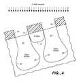
- FIG. 4is a fragmentary vertical cross-sectional view illustrating an alternate way of forming the structure of FIG. 3, with the substrate tilted with respect to the axis of the implant beam during the implantation, so that the lower regions of the deep N wells will be formed wider than the top portions of the N wells to enhance the collection of free electrons by the deep N wells.
- the inventioncomprises an improved integrated circuit structure such as an SRAM having a reduced soft error rate formed in a semiconductor substrate, wherein at least one N channel transistor is built in a P well adjacent to at least one deep N well connected to the high voltage supply and the deep N well extends from the surface of the substrate down into the substrate to a depth at least equal to that depth at which alpha particle-generated electron-hole pairs can effectively cause a soft error in the SRAM cell.
- the depth at which alpha particle-generated electron-hole pairs can effectively cause a soft error in the SRAM cellis from 0.5 to 3 ⁇ m.
- the deep N well of the 0.25 ⁇ m SRAM designtherefore, extends down from the substrate surface a distance of at least about 1 ⁇ m, and preferably at least about 2 ⁇ m.
- the implantation of the substrate to form the deep N well of the improved SRAM of the inventionis carried out in a manner which will cause lateral straggle, i.e., cause the doped volume comprising the N well to broaden at its base.
- Such a broadened base deep N wellwill have enhanced opportunity to collect electrons generated by the alpha particle collision with the substrate.
- This deep N well with a broadened basecan be formed either by increasing the implant energy or by tilting the substrate with respect to the axis of the implant beam while implanting the substrate to form the deep N well.
- the depth of the P wells and N wells referred to herein, including the “deep N wells” of the invention,is defined as the distance between the surface of the substrate to the peak (Rp) of the dopant used to form the well.
- deep N wellis intended to define an N well having a depth at least equal to the horizontal spacing from the deep N well to the next N well.
- the depth of the N wellis only about 0.4 times the horizontal spacing between N wells.
- FIG. 2wherein the same numerals are used to describe the same features previously described with respect to FIG. 1, the shallow N wells 8 and 12 of the prior art SRAM structure of FIG. 1 have been replaced by deep N wells 50 and 54 having a depth at least equal to or larger than the horizontal spacing between deep N wells 50 and 54 .
- the depth of deep N wells 50 and 54will range from as least about twice the horizontal spacing between deep N wells 50 and 54 up to four or more times the horizontal spacing between deep N wells 50 and 54 .
- the depth of deep N wells 50 and 54will be at least about 1 ⁇ m, and preferably will range from at least about 2 ⁇ m up to 4 ⁇ m or more in depth from the surface of substrate 2 .
- Deep N wells 50 and 54may be formed by implanting silicon substrate 2 with an N type dopant such as phosphorus or arsenic.
- an N type dopantsuch as phosphorus or arsenic.
- the dopantmay be implanted using a single energy level ranging from about 100 KeV up to about 300 KeV, as well as multiple implants ranging from 100 to 1000 KeV, depending upon the desired depth of the deep N wells. It should be pointed out that the thickness of the resist mask used to protect other portions of the substrate from the implant beam will have to be increased accordingly when higher implant energies are used to form the desired deep N wells (see thick resist mask 70 shown in FIGS. 3 - 4 ).
- the electrons in such electron-hole pairswill be influenced by the space charge region between the deep N wells of the invention and the substrate, and the electric field will drift the electrons toward the deep N wells until they are collected by the deep N wells. Since the majority of such electrons will be collected by the deep N wells, the possibility of electrons diffusing upward to the surface and into the N+ diffusion regions is greatly reduced, resulting in a corresponding reduction in the soft error rate, and immunity to alpha-particle impaction is therefore improved.
- FIG. 3a preferred embodiment of the invention is illustrated comprising a deep N well 60 having an enlarged lower portion or straggle shown at 62 , and a deep N well 64 having an enlarged lower portion or straggle shown at 66 .
- Such enlarged lower portions or stragglewill inherently occur to some extent as a function of the depth of the implant. That is, the deeper the implant, the more likely that the dopant pattern implanted into the substrate will tend to enlarge or result in a “straggle” of dopant atoms, due to scattering of the implanted dopant atoms and/or impact of the silicon atoms of the substrate by the implanted dopant atoms.
- N wells 60 and 64are still spaced from one another, i.e., the two N wells do not touch or overlap. This is very important for proper operation of the SRAM.
- a potentialis applied between the N well (e.g., at V DD potential) and the substrate (e.g., at V SS potential)
- a depletion regionwill form at the N-P junction between the deep N well and the P-type substrate. Forming this depletion region during operation of the SRAM cell is important to proper function of the cell.
- the distance which must be maintained between such enlarged portions of the respective deep N wellsmay be defined as that difference which will still permit formation of an N-P depletion region between the deep N well and the P type substrate when a potential is applied between the deep N well and the substrate.
- the respective deep N wellsextend as close as possible to one another without jeopardizing the formation of the above discussed depletion regions.
- the naturally occurring straggle of the dopantmay not result in the desired amount of lateral extension of the deep N wells toward each other.
- the lateral extension of the deep N wells toward one anothermay be further increased by tilting the substrate during the implant with respect to the axis of the implant beam which is normally perpendicular to the plane of the substrate.
- the maximum extent of the tiltwill again be governed by the extent of the resulting lateral extension of the N wells toward one another, with the maximum tilt not exceeding that angle which will still allow individual deep N wells to be formed without touching one another as determined by the ability to still form the desired respective (and separated) depletion regions between the deep N wells and the P type substrate.
- the substrateis first tilted one way, as shown in FIG. 4, and then rotated to tilt the substrate the same amount in the opposite direction, e.g., first tilted ⁇ 30° counterclockwise to the horizontal, as shown in FIG. 4, and then tilted ⁇ 30° clockwise to the horizontal prior to the implant.
- deep N wells 62 and 66may be allowed to connect or overlap one another provided that P well 10 is connected to Vss (the lowest supplied voltage in the circuitry) by a surface contact in order to define the electrical potential on P well 10 .
- the inventionprovides an integrated circuit structure such as an SRAM structure wherein deep N wells which extend down from the substrate surface to a depth at least equal to the horizontal spacing between the deep N wells provide the structure with enhanced protection against the occurrence of soft errors resulting from penetration of the structure by alpha-particles. Electrons in the substrate resulting from the electron-hole pairs generated by such alpha-particle penetration are attracted to the deep N wells by the electric field set up between the deep N wells and the substrate, and thus do not reach the N+ regions of the N channel transistor constructed in the P well, thus inhibiting the occurrence of soft errors such as, for example, in reading the on-off state of an SRAM cell.
Landscapes
- Metal-Oxide And Bipolar Metal-Oxide Semiconductor Integrated Circuits (AREA)
- Semiconductor Memories (AREA)
Abstract
Description
Claims (13)
Priority Applications (1)
| Application Number | Priority Date | Filing Date | Title |
|---|---|---|---|
| US09/675,109US6472715B1 (en) | 2000-09-28 | 2000-09-28 | Reduced soft error rate (SER) construction for integrated circuit structures |
Applications Claiming Priority (1)
| Application Number | Priority Date | Filing Date | Title |
|---|---|---|---|
| US09/675,109US6472715B1 (en) | 2000-09-28 | 2000-09-28 | Reduced soft error rate (SER) construction for integrated circuit structures |
Publications (1)
| Publication Number | Publication Date |
|---|---|
| US6472715B1true US6472715B1 (en) | 2002-10-29 |
Family
ID=24709095
Family Applications (1)
| Application Number | Title | Priority Date | Filing Date |
|---|---|---|---|
| US09/675,109Expired - LifetimeUS6472715B1 (en) | 2000-09-28 | 2000-09-28 | Reduced soft error rate (SER) construction for integrated circuit structures |
Country Status (1)
| Country | Link |
|---|---|
| US (1) | US6472715B1 (en) |
Cited By (12)
| Publication number | Priority date | Publication date | Assignee | Title |
|---|---|---|---|---|
| US20050079668A1 (en)* | 2003-10-09 | 2005-04-14 | Hyuck-Chai Jung | Semiconductor device having a well structure for improving soft error rate immunity and latch-up immunity and a method of making such a device |
| US20050098835A1 (en)* | 2003-11-06 | 2005-05-12 | Nec Electronics Corporation | Semiconductor device and semiconductor integrated circuit device |
| US20050179093A1 (en)* | 2004-02-17 | 2005-08-18 | Silicon Space Technology Corporation | Buried guard ring and radiation hardened isolation structures and fabrication methods |
| US20060049464A1 (en)* | 2004-09-03 | 2006-03-09 | Rao G R Mohan | Semiconductor devices with graded dopant regions |
| US20060073685A1 (en)* | 2004-10-01 | 2006-04-06 | Texas Instruments Incorporated | Method for implanting dopants within a substrate by tilting the substrate relative to the implant source |
| US20060164130A1 (en)* | 2005-01-17 | 2006-07-27 | Kabushiki Kaisha Toshiba | Semiconductor integrated circuit device |
| US7230303B1 (en) | 2004-10-15 | 2007-06-12 | Gsi Technology, Inc. | Semiconductor memory device with reduced soft error rate (SER) and method for fabricating same |
| US20070141794A1 (en)* | 2005-10-14 | 2007-06-21 | Silicon Space Technology Corporation | Radiation hardened isolation structures and fabrication methods |
| US20080142899A1 (en)* | 2006-08-04 | 2008-06-19 | Silicon Space Technology Corporation | Radiation immunity of integrated circuits using backside die contact and electrically conductive layers |
| US7921400B1 (en) | 2005-07-20 | 2011-04-05 | Integrated Device Technology, Inc. | Method for forming integrated circuit device using cell library with soft error resistant logic cells |
| US20110180878A1 (en)* | 2010-01-27 | 2011-07-28 | System General Corp. | High Side Semiconductor Structure |
| US10038058B2 (en) | 2016-05-07 | 2018-07-31 | Silicon Space Technology Corporation | FinFET device structure and method for forming same |
Citations (10)
| Publication number | Priority date | Publication date | Assignee | Title |
|---|---|---|---|---|
| JPS63301559A (en)* | 1987-01-30 | 1988-12-08 | Hitachi Ltd | semiconductor equipment |
| US4864382A (en)* | 1987-01-30 | 1989-09-05 | Hitachi, Ltd. | Semiconductor device |
| US5338963A (en)* | 1993-04-05 | 1994-08-16 | International Business Machines Corporation | Soft error immune CMOS static RAM cell |
| US5731619A (en)* | 1996-05-22 | 1998-03-24 | International Business Machines Corporation | CMOS structure with FETS having isolated wells with merged depletions and methods of making same |
| US5780907A (en)* | 1994-09-22 | 1998-07-14 | Fujitsu Limited | Semiconductor device having triple wells |
| JP2000172231A (en)* | 1998-12-01 | 2000-06-23 | Mitsubishi Electric Corp | Matrix display data line drive circuit |
| US6087849A (en)* | 1998-09-23 | 2000-07-11 | Intel Corporation | Soft error immunity in CMOS circuits with large shared diffusion areas |
| US6169318B1 (en)* | 1998-02-23 | 2001-01-02 | Polaroid Corporation | CMOS imager with improved sensitivity |
| US6281554B1 (en)* | 2000-03-20 | 2001-08-28 | United Microelectronics Corp. | Electrostatic discharge protection circuit |
| US6329693B1 (en)* | 1999-06-09 | 2001-12-11 | Seiko Epson Corporation | Semiconductor memory device and method of manufacturing the same |
- 2000
- 2000-09-28USUS09/675,109patent/US6472715B1/ennot_activeExpired - Lifetime
Patent Citations (10)
| Publication number | Priority date | Publication date | Assignee | Title |
|---|---|---|---|---|
| JPS63301559A (en)* | 1987-01-30 | 1988-12-08 | Hitachi Ltd | semiconductor equipment |
| US4864382A (en)* | 1987-01-30 | 1989-09-05 | Hitachi, Ltd. | Semiconductor device |
| US5338963A (en)* | 1993-04-05 | 1994-08-16 | International Business Machines Corporation | Soft error immune CMOS static RAM cell |
| US5780907A (en)* | 1994-09-22 | 1998-07-14 | Fujitsu Limited | Semiconductor device having triple wells |
| US5731619A (en)* | 1996-05-22 | 1998-03-24 | International Business Machines Corporation | CMOS structure with FETS having isolated wells with merged depletions and methods of making same |
| US6169318B1 (en)* | 1998-02-23 | 2001-01-02 | Polaroid Corporation | CMOS imager with improved sensitivity |
| US6087849A (en)* | 1998-09-23 | 2000-07-11 | Intel Corporation | Soft error immunity in CMOS circuits with large shared diffusion areas |
| JP2000172231A (en)* | 1998-12-01 | 2000-06-23 | Mitsubishi Electric Corp | Matrix display data line drive circuit |
| US6329693B1 (en)* | 1999-06-09 | 2001-12-11 | Seiko Epson Corporation | Semiconductor memory device and method of manufacturing the same |
| US6281554B1 (en)* | 2000-03-20 | 2001-08-28 | United Microelectronics Corp. | Electrostatic discharge protection circuit |
Non-Patent Citations (2)
| Title |
|---|
| Matsuda, Y., et al., "MeV-Boron Implanted Buried Barrier for Soft Error Reduction in Megabit DRAM", Extended Abstracts of the 19th Conference on Solid State Devices and Materials, Tokyo, 1987, pp. 23-26. |
| Yamashita, Tomohiro, et al., "Substrate Engineering for Reduction of Alpha-particle-Induced Charge Collection Efficiency", Jpn. J. Appl. Phys., vol. 35, 1996, pp. 869-873. |
Cited By (34)
| Publication number | Priority date | Publication date | Assignee | Title |
|---|---|---|---|---|
| US7294889B2 (en) | 2003-10-09 | 2007-11-13 | Samsung Electronics Co., Ltd. | Semiconductor device having a well structure for improving soft error rate immunity and latch-up immunity and a method of making such a device |
| US20050079668A1 (en)* | 2003-10-09 | 2005-04-14 | Hyuck-Chai Jung | Semiconductor device having a well structure for improving soft error rate immunity and latch-up immunity and a method of making such a device |
| US7214989B2 (en) | 2003-11-06 | 2007-05-08 | Nec Electronics Corporation | Semiconductor device and semiconductor integrated circuit device |
| US20050098835A1 (en)* | 2003-11-06 | 2005-05-12 | Nec Electronics Corporation | Semiconductor device and semiconductor integrated circuit device |
| US20060249759A1 (en)* | 2004-02-17 | 2006-11-09 | Morris Wesley H | Buried guard ring and radiation hardened isolation structures and fabrication methods |
| US8093145B2 (en) | 2004-02-17 | 2012-01-10 | Silicon Space Technology Corp. | Methods for operating and fabricating a semiconductor device having a buried guard ring structure |
| US20080188045A1 (en)* | 2004-02-17 | 2008-08-07 | Morris Wesley H | Methods for operating and fabricating a semiconductor device having a buried guard ring structure |
| US8729640B2 (en) | 2004-02-17 | 2014-05-20 | Silicon Space Technology Corporation | Method and structure for radiation hardening a semiconductor device |
| US7804138B2 (en) | 2004-02-17 | 2010-09-28 | Silicon Space Technology Corp. | Buried guard ring and radiation hardened isolation structures and fabrication methods |
| US7629654B2 (en) | 2004-02-17 | 2009-12-08 | Silicon Space Technology Corp. | Buried guard ring structures and fabrication methods |
| US8497195B2 (en) | 2004-02-17 | 2013-07-30 | Silicon Space Technology Corporation | Method for radiation hardening a semiconductor device |
| US20050179093A1 (en)* | 2004-02-17 | 2005-08-18 | Silicon Space Technology Corporation | Buried guard ring and radiation hardened isolation structures and fabrication methods |
| US7304354B2 (en) | 2004-02-17 | 2007-12-04 | Silicon Space Technology Corp. | Buried guard ring and radiation hardened isolation structures and fabrication methods |
| US20080073725A1 (en)* | 2004-02-17 | 2008-03-27 | Morris Wesley H | Buried guard ring structures and fabrication methods |
| US11121222B2 (en) | 2004-09-03 | 2021-09-14 | Greenthread, Llc | Semiconductor devices with graded dopant regions |
| US10510842B2 (en) | 2004-09-03 | 2019-12-17 | Greenthread, Llc | Semiconductor devices with graded dopant regions |
| US10734481B2 (en) | 2004-09-03 | 2020-08-04 | Greenthread, Llc | Semiconductor devices with graded dopant regions |
| US9647070B2 (en) | 2004-09-03 | 2017-05-09 | Greenthread, Llc | Semiconductor devices with graded dopant regions |
| US20060049464A1 (en)* | 2004-09-03 | 2006-03-09 | Rao G R Mohan | Semiconductor devices with graded dopant regions |
| US7232744B2 (en)* | 2004-10-01 | 2007-06-19 | Texas Instruments Incorporated | Method for implanting dopants within a substrate by tilting the substrate relative to the implant source |
| US20060073685A1 (en)* | 2004-10-01 | 2006-04-06 | Texas Instruments Incorporated | Method for implanting dopants within a substrate by tilting the substrate relative to the implant source |
| US7230303B1 (en) | 2004-10-15 | 2007-06-12 | Gsi Technology, Inc. | Semiconductor memory device with reduced soft error rate (SER) and method for fabricating same |
| US7504703B2 (en) | 2005-01-17 | 2009-03-17 | Kabushiki Kaisha Toshiba | Semiconductor integrated circuit device |
| US20060164130A1 (en)* | 2005-01-17 | 2006-07-27 | Kabushiki Kaisha Toshiba | Semiconductor integrated circuit device |
| US7921400B1 (en) | 2005-07-20 | 2011-04-05 | Integrated Device Technology, Inc. | Method for forming integrated circuit device using cell library with soft error resistant logic cells |
| US8252642B2 (en) | 2005-10-14 | 2012-08-28 | Silicon Space Technology Corp. | Fabrication methods for radiation hardened isolation structures |
| US8278719B2 (en) | 2005-10-14 | 2012-10-02 | Silicon Space Technology Corp. | Radiation hardened isolation structures and fabrication methods |
| US20100267212A1 (en)* | 2005-10-14 | 2010-10-21 | Morris Wesley H | Fabrication methods for radiation hardened isolation structures |
| US20070141794A1 (en)* | 2005-10-14 | 2007-06-21 | Silicon Space Technology Corporation | Radiation hardened isolation structures and fabrication methods |
| US20080142899A1 (en)* | 2006-08-04 | 2008-06-19 | Silicon Space Technology Corporation | Radiation immunity of integrated circuits using backside die contact and electrically conductive layers |
| US8492849B2 (en)* | 2010-01-27 | 2013-07-23 | System General Corp. | High side semiconductor structure |
| US20110180878A1 (en)* | 2010-01-27 | 2011-07-28 | System General Corp. | High Side Semiconductor Structure |
| US10038058B2 (en) | 2016-05-07 | 2018-07-31 | Silicon Space Technology Corporation | FinFET device structure and method for forming same |
| US10615260B1 (en) | 2016-05-07 | 2020-04-07 | Silicon Space Technology Corporation | Method for forming FinFET device structure |
Similar Documents
| Publication | Publication Date | Title |
|---|---|---|
| US10615260B1 (en) | Method for forming FinFET device structure | |
| US6586798B1 (en) | High voltage MOS-gated power device | |
| US8729640B2 (en) | Method and structure for radiation hardening a semiconductor device | |
| US6472715B1 (en) | Reduced soft error rate (SER) construction for integrated circuit structures | |
| Schwank et al. | BUSFET-a radiation-hardened SOI transistor | |
| JPS58107667A (en) | Semiconductor integrated circuit device | |
| US4115794A (en) | Charge pumping device with integrated regulating capacitor and method for making same | |
| US7214989B2 (en) | Semiconductor device and semiconductor integrated circuit device | |
| JP2634163B2 (en) | Semiconductor storage device | |
| Lim et al. | Improvement of GIDL-assisted Erase by using Surrounded BL PAD Structure for VNAND | |
| US7105413B2 (en) | Methods for forming super-steep diffusion region profiles in MOS devices and resulting semiconductor topographies | |
| US4135289A (en) | Method for producing a buried junction memory device | |
| US7554130B1 (en) | Reducing effects of parasitic transistors in thyristor-based memory using an isolation or damage region | |
| US6064098A (en) | Semiconductor processing methods of forming complementary metal oxide semiconductor memory and other circuitry, and memory and other circuitry | |
| US7894256B1 (en) | Thyristor based memory cell | |
| JPS61229353A (en) | Integrated circuit type dynamic memory | |
| US5049966A (en) | Lateral transistor beta reduction by incorporation of electrically active material | |
| JPS61229352A (en) | Ic type dynamic memory and manufacture thereof | |
| JP2002033403A (en) | Static semiconductor memory device | |
| SER | Liu et al. | |
| KR100755105B1 (en) | Semiconductor device | |
| KR900006019B1 (en) | Method of manufacturing semiconductor device | |
| US7230303B1 (en) | Semiconductor memory device with reduced soft error rate (SER) and method for fabricating same | |
| US5027167A (en) | Semiconductor intergrated circuit | |
| JP2011054772A (en) | Semiconductor device |
Legal Events
| Date | Code | Title | Description |
|---|---|---|---|
| AS | Assignment | Owner name:LSI LOGIC CORPORATION, CALIFORNIA Free format text:ASSIGNMENT OF ASSIGNORS INTEREST;ASSIGNORS:LIU, YAUH-CHING;PUCHNER, HELMUT;CASTAGNETTI, RUGGERO;AND OTHERS;REEL/FRAME:011168/0351;SIGNING DATES FROM 20000830 TO 20000925 | |
| STCF | Information on status: patent grant | Free format text:PATENTED CASE | |
| FPAY | Fee payment | Year of fee payment:4 | |
| FEPP | Fee payment procedure | Free format text:PAYOR NUMBER ASSIGNED (ORIGINAL EVENT CODE: ASPN); ENTITY STATUS OF PATENT OWNER: LARGE ENTITY | |
| FPAY | Fee payment | Year of fee payment:8 | |
| FPAY | Fee payment | Year of fee payment:12 | |
| AS | Assignment | Owner name:DEUTSCHE BANK AG NEW YORK BRANCH, AS COLLATERAL AG Free format text:PATENT SECURITY AGREEMENT;ASSIGNORS:LSI CORPORATION;AGERE SYSTEMS LLC;REEL/FRAME:032856/0031 Effective date:20140506 | |
| AS | Assignment | Owner name:LSI CORPORATION, CALIFORNIA Free format text:CHANGE OF NAME;ASSIGNOR:LSI LOGIC CORPORATION;REEL/FRAME:033102/0270 Effective date:20070406 | |
| AS | Assignment | Owner name:AVAGO TECHNOLOGIES GENERAL IP (SINGAPORE) PTE. LTD Free format text:ASSIGNMENT OF ASSIGNORS INTEREST;ASSIGNOR:LSI CORPORATION;REEL/FRAME:035390/0388 Effective date:20140814 | |
| AS | Assignment | Owner name:AGERE SYSTEMS LLC, PENNSYLVANIA Free format text:TERMINATION AND RELEASE OF SECURITY INTEREST IN PATENT RIGHTS (RELEASES RF 032856-0031);ASSIGNOR:DEUTSCHE BANK AG NEW YORK BRANCH, AS COLLATERAL AGENT;REEL/FRAME:037684/0039 Effective date:20160201 Owner name:LSI CORPORATION, CALIFORNIA Free format text:TERMINATION AND RELEASE OF SECURITY INTEREST IN PATENT RIGHTS (RELEASES RF 032856-0031);ASSIGNOR:DEUTSCHE BANK AG NEW YORK BRANCH, AS COLLATERAL AGENT;REEL/FRAME:037684/0039 Effective date:20160201 | |
| AS | Assignment | Owner name:BANK OF AMERICA, N.A., AS COLLATERAL AGENT, NORTH CAROLINA Free format text:PATENT SECURITY AGREEMENT;ASSIGNOR:AVAGO TECHNOLOGIES GENERAL IP (SINGAPORE) PTE. LTD.;REEL/FRAME:037808/0001 Effective date:20160201 Owner name:BANK OF AMERICA, N.A., AS COLLATERAL AGENT, NORTH Free format text:PATENT SECURITY AGREEMENT;ASSIGNOR:AVAGO TECHNOLOGIES GENERAL IP (SINGAPORE) PTE. LTD.;REEL/FRAME:037808/0001 Effective date:20160201 | |
| AS | Assignment | Owner name:AVAGO TECHNOLOGIES GENERAL IP (SINGAPORE) PTE. LTD., SINGAPORE Free format text:TERMINATION AND RELEASE OF SECURITY INTEREST IN PATENTS;ASSIGNOR:BANK OF AMERICA, N.A., AS COLLATERAL AGENT;REEL/FRAME:041710/0001 Effective date:20170119 Owner name:AVAGO TECHNOLOGIES GENERAL IP (SINGAPORE) PTE. LTD Free format text:TERMINATION AND RELEASE OF SECURITY INTEREST IN PATENTS;ASSIGNOR:BANK OF AMERICA, N.A., AS COLLATERAL AGENT;REEL/FRAME:041710/0001 Effective date:20170119 | |
| AS | Assignment | Owner name:BELL SEMICONDUCTOR, LLC, ILLINOIS Free format text:ASSIGNMENT OF ASSIGNORS INTEREST;ASSIGNORS:AVAGO TECHNOLOGIES GENERAL IP (SINGAPORE) PTE. LTD.;BROADCOM CORPORATION;REEL/FRAME:044886/0001 Effective date:20171208 | |
| AS | Assignment | Owner name:CORTLAND CAPITAL MARKET SERVICES LLC, AS COLLATERA Free format text:SECURITY INTEREST;ASSIGNORS:HILCO PATENT ACQUISITION 56, LLC;BELL SEMICONDUCTOR, LLC;BELL NORTHERN RESEARCH, LLC;REEL/FRAME:045216/0020 Effective date:20180124 | |
| AS | Assignment | Owner name:BELL NORTHERN RESEARCH, LLC, ILLINOIS Free format text:SECURITY INTEREST;ASSIGNOR:CORTLAND CAPITAL MARKET SERVICES LLC;REEL/FRAME:060885/0001 Effective date:20220401 Owner name:BELL SEMICONDUCTOR, LLC, ILLINOIS Free format text:SECURITY INTEREST;ASSIGNOR:CORTLAND CAPITAL MARKET SERVICES LLC;REEL/FRAME:060885/0001 Effective date:20220401 Owner name:HILCO PATENT ACQUISITION 56, LLC, ILLINOIS Free format text:SECURITY INTEREST;ASSIGNOR:CORTLAND CAPITAL MARKET SERVICES LLC;REEL/FRAME:060885/0001 Effective date:20220401 |