US6472304B2 - Wire bonding to copper - Google Patents
Wire bonding to copperDownload PDFInfo
- Publication number
- US6472304B2 US6472304B2US09/864,577US86457701AUS6472304B2US 6472304 B2US6472304 B2US 6472304B2US 86457701 AUS86457701 AUS 86457701AUS 6472304 B2US6472304 B2US 6472304B2
- Authority
- US
- United States
- Prior art keywords
- layer
- copper
- planar
- depositing
- barrier layer
- Prior art date
- Legal status (The legal status is an assumption and is not a legal conclusion. Google has not performed a legal analysis and makes no representation as to the accuracy of the status listed.)
- Expired - Lifetime
Links
Images


Classifications
- H—ELECTRICITY
- H01—ELECTRIC ELEMENTS
- H01L—SEMICONDUCTOR DEVICES NOT COVERED BY CLASS H10
- H01L24/00—Arrangements for connecting or disconnecting semiconductor or solid-state bodies; Methods or apparatus related thereto
- H01L24/80—Methods for connecting semiconductor or other solid state bodies using means for bonding being attached to, or being formed on, the surface to be connected
- H01L24/85—Methods for connecting semiconductor or other solid state bodies using means for bonding being attached to, or being formed on, the surface to be connected using a wire connector
- H—ELECTRICITY
- H01—ELECTRIC ELEMENTS
- H01L—SEMICONDUCTOR DEVICES NOT COVERED BY CLASS H10
- H01L21/00—Processes or apparatus adapted for the manufacture or treatment of semiconductor or solid state devices or of parts thereof
- H01L21/02—Manufacture or treatment of semiconductor devices or of parts thereof
- H01L21/04—Manufacture or treatment of semiconductor devices or of parts thereof the devices having potential barriers, e.g. a PN junction, depletion layer or carrier concentration layer
- H01L21/50—Assembly of semiconductor devices using processes or apparatus not provided for in a single one of the groups H01L21/18 - H01L21/326 or H10D48/04 - H10D48/07 e.g. sealing of a cap to a base of a container
- H01L21/60—Attaching or detaching leads or other conductive members, to be used for carrying current to or from the device in operation
- H—ELECTRICITY
- H01—ELECTRIC ELEMENTS
- H01L—SEMICONDUCTOR DEVICES NOT COVERED BY CLASS H10
- H01L24/00—Arrangements for connecting or disconnecting semiconductor or solid-state bodies; Methods or apparatus related thereto
- H01L24/01—Means for bonding being attached to, or being formed on, the surface to be connected, e.g. chip-to-package, die-attach, "first-level" interconnects; Manufacturing methods related thereto
- H01L24/02—Bonding areas ; Manufacturing methods related thereto
- H01L24/03—Manufacturing methods
- H—ELECTRICITY
- H01—ELECTRIC ELEMENTS
- H01L—SEMICONDUCTOR DEVICES NOT COVERED BY CLASS H10
- H01L24/00—Arrangements for connecting or disconnecting semiconductor or solid-state bodies; Methods or apparatus related thereto
- H01L24/01—Means for bonding being attached to, or being formed on, the surface to be connected, e.g. chip-to-package, die-attach, "first-level" interconnects; Manufacturing methods related thereto
- H01L24/02—Bonding areas ; Manufacturing methods related thereto
- H01L24/04—Structure, shape, material or disposition of the bonding areas prior to the connecting process
- H01L24/05—Structure, shape, material or disposition of the bonding areas prior to the connecting process of an individual bonding area
- H—ELECTRICITY
- H01—ELECTRIC ELEMENTS
- H01L—SEMICONDUCTOR DEVICES NOT COVERED BY CLASS H10
- H01L24/00—Arrangements for connecting or disconnecting semiconductor or solid-state bodies; Methods or apparatus related thereto
- H01L24/01—Means for bonding being attached to, or being formed on, the surface to be connected, e.g. chip-to-package, die-attach, "first-level" interconnects; Manufacturing methods related thereto
- H01L24/42—Wire connectors; Manufacturing methods related thereto
- H01L24/47—Structure, shape, material or disposition of the wire connectors after the connecting process
- H01L24/48—Structure, shape, material or disposition of the wire connectors after the connecting process of an individual wire connector
- H—ELECTRICITY
- H01—ELECTRIC ELEMENTS
- H01L—SEMICONDUCTOR DEVICES NOT COVERED BY CLASS H10
- H01L2224/00—Indexing scheme for arrangements for connecting or disconnecting semiconductor or solid-state bodies and methods related thereto as covered by H01L24/00
- H01L2224/01—Means for bonding being attached to, or being formed on, the surface to be connected, e.g. chip-to-package, die-attach, "first-level" interconnects; Manufacturing methods related thereto
- H01L2224/02—Bonding areas; Manufacturing methods related thereto
- H01L2224/0212—Auxiliary members for bonding areas, e.g. spacers
- H01L2224/02122—Auxiliary members for bonding areas, e.g. spacers being formed on the semiconductor or solid-state body
- H01L2224/02163—Auxiliary members for bonding areas, e.g. spacers being formed on the semiconductor or solid-state body on the bonding area
- H01L2224/02165—Reinforcing structures
- H01L2224/02166—Collar structures
- H—ELECTRICITY
- H01—ELECTRIC ELEMENTS
- H01L—SEMICONDUCTOR DEVICES NOT COVERED BY CLASS H10
- H01L2224/00—Indexing scheme for arrangements for connecting or disconnecting semiconductor or solid-state bodies and methods related thereto as covered by H01L24/00
- H01L2224/01—Means for bonding being attached to, or being formed on, the surface to be connected, e.g. chip-to-package, die-attach, "first-level" interconnects; Manufacturing methods related thereto
- H01L2224/02—Bonding areas; Manufacturing methods related thereto
- H01L2224/04—Structure, shape, material or disposition of the bonding areas prior to the connecting process
- H01L2224/04042—Bonding areas specifically adapted for wire connectors, e.g. wirebond pads
- H—ELECTRICITY
- H01—ELECTRIC ELEMENTS
- H01L—SEMICONDUCTOR DEVICES NOT COVERED BY CLASS H10
- H01L2224/00—Indexing scheme for arrangements for connecting or disconnecting semiconductor or solid-state bodies and methods related thereto as covered by H01L24/00
- H01L2224/01—Means for bonding being attached to, or being formed on, the surface to be connected, e.g. chip-to-package, die-attach, "first-level" interconnects; Manufacturing methods related thereto
- H01L2224/02—Bonding areas; Manufacturing methods related thereto
- H01L2224/04—Structure, shape, material or disposition of the bonding areas prior to the connecting process
- H01L2224/05—Structure, shape, material or disposition of the bonding areas prior to the connecting process of an individual bonding area
- H01L2224/05001—Internal layers
- H01L2224/05005—Structure
- H01L2224/05009—Bonding area integrally formed with a via connection of the semiconductor or solid-state body
- H—ELECTRICITY
- H01—ELECTRIC ELEMENTS
- H01L—SEMICONDUCTOR DEVICES NOT COVERED BY CLASS H10
- H01L2224/00—Indexing scheme for arrangements for connecting or disconnecting semiconductor or solid-state bodies and methods related thereto as covered by H01L24/00
- H01L2224/01—Means for bonding being attached to, or being formed on, the surface to be connected, e.g. chip-to-package, die-attach, "first-level" interconnects; Manufacturing methods related thereto
- H01L2224/02—Bonding areas; Manufacturing methods related thereto
- H01L2224/04—Structure, shape, material or disposition of the bonding areas prior to the connecting process
- H01L2224/05—Structure, shape, material or disposition of the bonding areas prior to the connecting process of an individual bonding area
- H01L2224/05001—Internal layers
- H01L2224/0502—Disposition
- H01L2224/05026—Disposition the internal layer being disposed in a recess of the surface
- H01L2224/05027—Disposition the internal layer being disposed in a recess of the surface the internal layer extending out of an opening
- H—ELECTRICITY
- H01—ELECTRIC ELEMENTS
- H01L—SEMICONDUCTOR DEVICES NOT COVERED BY CLASS H10
- H01L2224/00—Indexing scheme for arrangements for connecting or disconnecting semiconductor or solid-state bodies and methods related thereto as covered by H01L24/00
- H01L2224/01—Means for bonding being attached to, or being formed on, the surface to be connected, e.g. chip-to-package, die-attach, "first-level" interconnects; Manufacturing methods related thereto
- H01L2224/02—Bonding areas; Manufacturing methods related thereto
- H01L2224/04—Structure, shape, material or disposition of the bonding areas prior to the connecting process
- H01L2224/05—Structure, shape, material or disposition of the bonding areas prior to the connecting process of an individual bonding area
- H01L2224/05001—Internal layers
- H01L2224/05075—Plural internal layers
- H01L2224/0508—Plural internal layers being stacked
- H01L2224/05082—Two-layer arrangements
- H—ELECTRICITY
- H01—ELECTRIC ELEMENTS
- H01L—SEMICONDUCTOR DEVICES NOT COVERED BY CLASS H10
- H01L2224/00—Indexing scheme for arrangements for connecting or disconnecting semiconductor or solid-state bodies and methods related thereto as covered by H01L24/00
- H01L2224/01—Means for bonding being attached to, or being formed on, the surface to be connected, e.g. chip-to-package, die-attach, "first-level" interconnects; Manufacturing methods related thereto
- H01L2224/02—Bonding areas; Manufacturing methods related thereto
- H01L2224/04—Structure, shape, material or disposition of the bonding areas prior to the connecting process
- H01L2224/05—Structure, shape, material or disposition of the bonding areas prior to the connecting process of an individual bonding area
- H01L2224/05001—Internal layers
- H01L2224/05099—Material
- H01L2224/051—Material with a principal constituent of the material being a metal or a metalloid, e.g. boron [B], silicon [Si], germanium [Ge], arsenic [As], antimony [Sb], tellurium [Te] and polonium [Po], and alloys thereof
- H01L2224/05163—Material with a principal constituent of the material being a metal or a metalloid, e.g. boron [B], silicon [Si], germanium [Ge], arsenic [As], antimony [Sb], tellurium [Te] and polonium [Po], and alloys thereof the principal constituent melting at a temperature of greater than 1550°C
- H01L2224/05166—Titanium [Ti] as principal constituent
- H—ELECTRICITY
- H01—ELECTRIC ELEMENTS
- H01L—SEMICONDUCTOR DEVICES NOT COVERED BY CLASS H10
- H01L2224/00—Indexing scheme for arrangements for connecting or disconnecting semiconductor or solid-state bodies and methods related thereto as covered by H01L24/00
- H01L2224/01—Means for bonding being attached to, or being formed on, the surface to be connected, e.g. chip-to-package, die-attach, "first-level" interconnects; Manufacturing methods related thereto
- H01L2224/02—Bonding areas; Manufacturing methods related thereto
- H01L2224/04—Structure, shape, material or disposition of the bonding areas prior to the connecting process
- H01L2224/05—Structure, shape, material or disposition of the bonding areas prior to the connecting process of an individual bonding area
- H01L2224/05001—Internal layers
- H01L2224/05099—Material
- H01L2224/051—Material with a principal constituent of the material being a metal or a metalloid, e.g. boron [B], silicon [Si], germanium [Ge], arsenic [As], antimony [Sb], tellurium [Te] and polonium [Po], and alloys thereof
- H01L2224/05163—Material with a principal constituent of the material being a metal or a metalloid, e.g. boron [B], silicon [Si], germanium [Ge], arsenic [As], antimony [Sb], tellurium [Te] and polonium [Po], and alloys thereof the principal constituent melting at a temperature of greater than 1550°C
- H01L2224/05181—Tantalum [Ta] as principal constituent
- H—ELECTRICITY
- H01—ELECTRIC ELEMENTS
- H01L—SEMICONDUCTOR DEVICES NOT COVERED BY CLASS H10
- H01L2224/00—Indexing scheme for arrangements for connecting or disconnecting semiconductor or solid-state bodies and methods related thereto as covered by H01L24/00
- H01L2224/01—Means for bonding being attached to, or being formed on, the surface to be connected, e.g. chip-to-package, die-attach, "first-level" interconnects; Manufacturing methods related thereto
- H01L2224/02—Bonding areas; Manufacturing methods related thereto
- H01L2224/04—Structure, shape, material or disposition of the bonding areas prior to the connecting process
- H01L2224/05—Structure, shape, material or disposition of the bonding areas prior to the connecting process of an individual bonding area
- H01L2224/05001—Internal layers
- H01L2224/05099—Material
- H01L2224/05186—Material with a principal constituent of the material being a non metallic, non metalloid inorganic material
- H01L2224/05187—Ceramics, e.g. crystalline carbides, nitrides or oxides
- H—ELECTRICITY
- H01—ELECTRIC ELEMENTS
- H01L—SEMICONDUCTOR DEVICES NOT COVERED BY CLASS H10
- H01L2224/00—Indexing scheme for arrangements for connecting or disconnecting semiconductor or solid-state bodies and methods related thereto as covered by H01L24/00
- H01L2224/01—Means for bonding being attached to, or being formed on, the surface to be connected, e.g. chip-to-package, die-attach, "first-level" interconnects; Manufacturing methods related thereto
- H01L2224/02—Bonding areas; Manufacturing methods related thereto
- H01L2224/04—Structure, shape, material or disposition of the bonding areas prior to the connecting process
- H01L2224/05—Structure, shape, material or disposition of the bonding areas prior to the connecting process of an individual bonding area
- H01L2224/0554—External layer
- H01L2224/0555—Shape
- H01L2224/05556—Shape in side view
- H01L2224/05558—Shape in side view conformal layer on a patterned surface
- H—ELECTRICITY
- H01—ELECTRIC ELEMENTS
- H01L—SEMICONDUCTOR DEVICES NOT COVERED BY CLASS H10
- H01L2224/00—Indexing scheme for arrangements for connecting or disconnecting semiconductor or solid-state bodies and methods related thereto as covered by H01L24/00
- H01L2224/01—Means for bonding being attached to, or being formed on, the surface to be connected, e.g. chip-to-package, die-attach, "first-level" interconnects; Manufacturing methods related thereto
- H01L2224/02—Bonding areas; Manufacturing methods related thereto
- H01L2224/04—Structure, shape, material or disposition of the bonding areas prior to the connecting process
- H01L2224/05—Structure, shape, material or disposition of the bonding areas prior to the connecting process of an individual bonding area
- H01L2224/0554—External layer
- H01L2224/0556—Disposition
- H01L2224/05571—Disposition the external layer being disposed in a recess of the surface
- H01L2224/05572—Disposition the external layer being disposed in a recess of the surface the external layer extending out of an opening
- H—ELECTRICITY
- H01—ELECTRIC ELEMENTS
- H01L—SEMICONDUCTOR DEVICES NOT COVERED BY CLASS H10
- H01L2224/00—Indexing scheme for arrangements for connecting or disconnecting semiconductor or solid-state bodies and methods related thereto as covered by H01L24/00
- H01L2224/01—Means for bonding being attached to, or being formed on, the surface to be connected, e.g. chip-to-package, die-attach, "first-level" interconnects; Manufacturing methods related thereto
- H01L2224/02—Bonding areas; Manufacturing methods related thereto
- H01L2224/04—Structure, shape, material or disposition of the bonding areas prior to the connecting process
- H01L2224/05—Structure, shape, material or disposition of the bonding areas prior to the connecting process of an individual bonding area
- H01L2224/0554—External layer
- H01L2224/05599—Material
- H01L2224/056—Material with a principal constituent of the material being a metal or a metalloid, e.g. boron [B], silicon [Si], germanium [Ge], arsenic [As], antimony [Sb], tellurium [Te] and polonium [Po], and alloys thereof
- H01L2224/05617—Material with a principal constituent of the material being a metal or a metalloid, e.g. boron [B], silicon [Si], germanium [Ge], arsenic [As], antimony [Sb], tellurium [Te] and polonium [Po], and alloys thereof the principal constituent melting at a temperature of greater than or equal to 400°C and less than 950°C
- H01L2224/05624—Aluminium [Al] as principal constituent
- H—ELECTRICITY
- H01—ELECTRIC ELEMENTS
- H01L—SEMICONDUCTOR DEVICES NOT COVERED BY CLASS H10
- H01L2224/00—Indexing scheme for arrangements for connecting or disconnecting semiconductor or solid-state bodies and methods related thereto as covered by H01L24/00
- H01L2224/01—Means for bonding being attached to, or being formed on, the surface to be connected, e.g. chip-to-package, die-attach, "first-level" interconnects; Manufacturing methods related thereto
- H01L2224/42—Wire connectors; Manufacturing methods related thereto
- H01L2224/44—Structure, shape, material or disposition of the wire connectors prior to the connecting process
- H01L2224/45—Structure, shape, material or disposition of the wire connectors prior to the connecting process of an individual wire connector
- H01L2224/45001—Core members of the connector
- H01L2224/4501—Shape
- H01L2224/45012—Cross-sectional shape
- H01L2224/45015—Cross-sectional shape being circular
- H—ELECTRICITY
- H01—ELECTRIC ELEMENTS
- H01L—SEMICONDUCTOR DEVICES NOT COVERED BY CLASS H10
- H01L2224/00—Indexing scheme for arrangements for connecting or disconnecting semiconductor or solid-state bodies and methods related thereto as covered by H01L24/00
- H01L2224/01—Means for bonding being attached to, or being formed on, the surface to be connected, e.g. chip-to-package, die-attach, "first-level" interconnects; Manufacturing methods related thereto
- H01L2224/42—Wire connectors; Manufacturing methods related thereto
- H01L2224/44—Structure, shape, material or disposition of the wire connectors prior to the connecting process
- H01L2224/45—Structure, shape, material or disposition of the wire connectors prior to the connecting process of an individual wire connector
- H01L2224/45001—Core members of the connector
- H01L2224/45099—Material
- H01L2224/451—Material with a principal constituent of the material being a metal or a metalloid, e.g. boron (B), silicon (Si), germanium (Ge), arsenic (As), antimony (Sb), tellurium (Te) and polonium (Po), and alloys thereof
- H01L2224/45117—Material with a principal constituent of the material being a metal or a metalloid, e.g. boron (B), silicon (Si), germanium (Ge), arsenic (As), antimony (Sb), tellurium (Te) and polonium (Po), and alloys thereof the principal constituent melting at a temperature of greater than or equal to 400°C and less than 950°C
- H01L2224/45124—Aluminium (Al) as principal constituent
- H—ELECTRICITY
- H01—ELECTRIC ELEMENTS
- H01L—SEMICONDUCTOR DEVICES NOT COVERED BY CLASS H10
- H01L2224/00—Indexing scheme for arrangements for connecting or disconnecting semiconductor or solid-state bodies and methods related thereto as covered by H01L24/00
- H01L2224/01—Means for bonding being attached to, or being formed on, the surface to be connected, e.g. chip-to-package, die-attach, "first-level" interconnects; Manufacturing methods related thereto
- H01L2224/42—Wire connectors; Manufacturing methods related thereto
- H01L2224/44—Structure, shape, material or disposition of the wire connectors prior to the connecting process
- H01L2224/45—Structure, shape, material or disposition of the wire connectors prior to the connecting process of an individual wire connector
- H01L2224/45001—Core members of the connector
- H01L2224/45099—Material
- H01L2224/451—Material with a principal constituent of the material being a metal or a metalloid, e.g. boron (B), silicon (Si), germanium (Ge), arsenic (As), antimony (Sb), tellurium (Te) and polonium (Po), and alloys thereof
- H01L2224/45138—Material with a principal constituent of the material being a metal or a metalloid, e.g. boron (B), silicon (Si), germanium (Ge), arsenic (As), antimony (Sb), tellurium (Te) and polonium (Po), and alloys thereof the principal constituent melting at a temperature of greater than or equal to 950°C and less than 1550°C
- H01L2224/45144—Gold (Au) as principal constituent
- H—ELECTRICITY
- H01—ELECTRIC ELEMENTS
- H01L—SEMICONDUCTOR DEVICES NOT COVERED BY CLASS H10
- H01L2224/00—Indexing scheme for arrangements for connecting or disconnecting semiconductor or solid-state bodies and methods related thereto as covered by H01L24/00
- H01L2224/01—Means for bonding being attached to, or being formed on, the surface to be connected, e.g. chip-to-package, die-attach, "first-level" interconnects; Manufacturing methods related thereto
- H01L2224/42—Wire connectors; Manufacturing methods related thereto
- H01L2224/44—Structure, shape, material or disposition of the wire connectors prior to the connecting process
- H01L2224/45—Structure, shape, material or disposition of the wire connectors prior to the connecting process of an individual wire connector
- H01L2224/45001—Core members of the connector
- H01L2224/45099—Material
- H01L2224/451—Material with a principal constituent of the material being a metal or a metalloid, e.g. boron (B), silicon (Si), germanium (Ge), arsenic (As), antimony (Sb), tellurium (Te) and polonium (Po), and alloys thereof
- H01L2224/45138—Material with a principal constituent of the material being a metal or a metalloid, e.g. boron (B), silicon (Si), germanium (Ge), arsenic (As), antimony (Sb), tellurium (Te) and polonium (Po), and alloys thereof the principal constituent melting at a temperature of greater than or equal to 950°C and less than 1550°C
- H01L2224/45147—Copper (Cu) as principal constituent
- H—ELECTRICITY
- H01—ELECTRIC ELEMENTS
- H01L—SEMICONDUCTOR DEVICES NOT COVERED BY CLASS H10
- H01L2224/00—Indexing scheme for arrangements for connecting or disconnecting semiconductor or solid-state bodies and methods related thereto as covered by H01L24/00
- H01L2224/01—Means for bonding being attached to, or being formed on, the surface to be connected, e.g. chip-to-package, die-attach, "first-level" interconnects; Manufacturing methods related thereto
- H01L2224/42—Wire connectors; Manufacturing methods related thereto
- H01L2224/47—Structure, shape, material or disposition of the wire connectors after the connecting process
- H01L2224/48—Structure, shape, material or disposition of the wire connectors after the connecting process of an individual wire connector
- H01L2224/484—Connecting portions
- H01L2224/4845—Details of ball bonds
- H01L2224/48451—Shape
- H01L2224/48453—Shape of the interface with the bonding area
- H—ELECTRICITY
- H01—ELECTRIC ELEMENTS
- H01L—SEMICONDUCTOR DEVICES NOT COVERED BY CLASS H10
- H01L2224/00—Indexing scheme for arrangements for connecting or disconnecting semiconductor or solid-state bodies and methods related thereto as covered by H01L24/00
- H01L2224/01—Means for bonding being attached to, or being formed on, the surface to be connected, e.g. chip-to-package, die-attach, "first-level" interconnects; Manufacturing methods related thereto
- H01L2224/42—Wire connectors; Manufacturing methods related thereto
- H01L2224/47—Structure, shape, material or disposition of the wire connectors after the connecting process
- H01L2224/48—Structure, shape, material or disposition of the wire connectors after the connecting process of an individual wire connector
- H01L2224/484—Connecting portions
- H01L2224/48463—Connecting portions the connecting portion on the bonding area of the semiconductor or solid-state body being a ball bond
- H—ELECTRICITY
- H01—ELECTRIC ELEMENTS
- H01L—SEMICONDUCTOR DEVICES NOT COVERED BY CLASS H10
- H01L2224/00—Indexing scheme for arrangements for connecting or disconnecting semiconductor or solid-state bodies and methods related thereto as covered by H01L24/00
- H01L2224/01—Means for bonding being attached to, or being formed on, the surface to be connected, e.g. chip-to-package, die-attach, "first-level" interconnects; Manufacturing methods related thereto
- H01L2224/42—Wire connectors; Manufacturing methods related thereto
- H01L2224/47—Structure, shape, material or disposition of the wire connectors after the connecting process
- H01L2224/48—Structure, shape, material or disposition of the wire connectors after the connecting process of an individual wire connector
- H01L2224/485—Material
- H01L2224/48505—Material at the bonding interface
- H01L2224/48599—Principal constituent of the connecting portion of the wire connector being Gold (Au)
- H01L2224/486—Principal constituent of the connecting portion of the wire connector being Gold (Au) with a principal constituent of the bonding area being a metal or a metalloid, e.g. boron (B), silicon (Si), germanium (Ge), arsenic (As), antimony (Sb), tellurium (Te) and polonium (Po), and alloys thereof
- H01L2224/48617—Principal constituent of the connecting portion of the wire connector being Gold (Au) with a principal constituent of the bonding area being a metal or a metalloid, e.g. boron (B), silicon (Si), germanium (Ge), arsenic (As), antimony (Sb), tellurium (Te) and polonium (Po), and alloys thereof the principal constituent melting at a temperature of greater than or equal to 400°C and less than 950 °C
- H01L2224/48624—Aluminium (Al) as principal constituent
- H—ELECTRICITY
- H01—ELECTRIC ELEMENTS
- H01L—SEMICONDUCTOR DEVICES NOT COVERED BY CLASS H10
- H01L2224/00—Indexing scheme for arrangements for connecting or disconnecting semiconductor or solid-state bodies and methods related thereto as covered by H01L24/00
- H01L2224/01—Means for bonding being attached to, or being formed on, the surface to be connected, e.g. chip-to-package, die-attach, "first-level" interconnects; Manufacturing methods related thereto
- H01L2224/42—Wire connectors; Manufacturing methods related thereto
- H01L2224/47—Structure, shape, material or disposition of the wire connectors after the connecting process
- H01L2224/48—Structure, shape, material or disposition of the wire connectors after the connecting process of an individual wire connector
- H01L2224/485—Material
- H01L2224/48505—Material at the bonding interface
- H01L2224/48699—Principal constituent of the connecting portion of the wire connector being Aluminium (Al)
- H01L2224/487—Principal constituent of the connecting portion of the wire connector being Aluminium (Al) with a principal constituent of the bonding area being a metal or a metalloid, e.g. boron (B), silicon (Si), germanium (Ge), arsenic (As), antimony (Sb), tellurium (Te) and polonium (Po), and alloys thereof
- H01L2224/48717—Principal constituent of the connecting portion of the wire connector being Aluminium (Al) with a principal constituent of the bonding area being a metal or a metalloid, e.g. boron (B), silicon (Si), germanium (Ge), arsenic (As), antimony (Sb), tellurium (Te) and polonium (Po), and alloys thereof the principal constituent melting at a temperature of greater than or equal to 400°C and less than 950 °C
- H01L2224/48724—Aluminium (Al) as principal constituent
- H—ELECTRICITY
- H01—ELECTRIC ELEMENTS
- H01L—SEMICONDUCTOR DEVICES NOT COVERED BY CLASS H10
- H01L2224/00—Indexing scheme for arrangements for connecting or disconnecting semiconductor or solid-state bodies and methods related thereto as covered by H01L24/00
- H01L2224/01—Means for bonding being attached to, or being formed on, the surface to be connected, e.g. chip-to-package, die-attach, "first-level" interconnects; Manufacturing methods related thereto
- H01L2224/42—Wire connectors; Manufacturing methods related thereto
- H01L2224/47—Structure, shape, material or disposition of the wire connectors after the connecting process
- H01L2224/48—Structure, shape, material or disposition of the wire connectors after the connecting process of an individual wire connector
- H01L2224/485—Material
- H01L2224/48505—Material at the bonding interface
- H01L2224/48799—Principal constituent of the connecting portion of the wire connector being Copper (Cu)
- H01L2224/488—Principal constituent of the connecting portion of the wire connector being Copper (Cu) with a principal constituent of the bonding area being a metal or a metalloid, e.g. boron (B), silicon (Si), germanium (Ge), arsenic (As), antimony (Sb), tellurium (Te) and polonium (Po), and alloys thereof
- H01L2224/48817—Principal constituent of the connecting portion of the wire connector being Copper (Cu) with a principal constituent of the bonding area being a metal or a metalloid, e.g. boron (B), silicon (Si), germanium (Ge), arsenic (As), antimony (Sb), tellurium (Te) and polonium (Po), and alloys thereof the principal constituent melting at a temperature of greater than or equal to 400°C and less than 950 °C
- H01L2224/48824—Aluminium (Al) as principal constituent
- H—ELECTRICITY
- H01—ELECTRIC ELEMENTS
- H01L—SEMICONDUCTOR DEVICES NOT COVERED BY CLASS H10
- H01L2224/00—Indexing scheme for arrangements for connecting or disconnecting semiconductor or solid-state bodies and methods related thereto as covered by H01L24/00
- H01L2224/80—Methods for connecting semiconductor or other solid state bodies using means for bonding being attached to, or being formed on, the surface to be connected
- H01L2224/85—Methods for connecting semiconductor or other solid state bodies using means for bonding being attached to, or being formed on, the surface to be connected using a wire connector
- H01L2224/852—Applying energy for connecting
- H01L2224/85201—Compression bonding
- H01L2224/85203—Thermocompression bonding
- H—ELECTRICITY
- H01—ELECTRIC ELEMENTS
- H01L—SEMICONDUCTOR DEVICES NOT COVERED BY CLASS H10
- H01L2224/00—Indexing scheme for arrangements for connecting or disconnecting semiconductor or solid-state bodies and methods related thereto as covered by H01L24/00
- H01L2224/80—Methods for connecting semiconductor or other solid state bodies using means for bonding being attached to, or being formed on, the surface to be connected
- H01L2224/85—Methods for connecting semiconductor or other solid state bodies using means for bonding being attached to, or being formed on, the surface to be connected using a wire connector
- H01L2224/852—Applying energy for connecting
- H01L2224/85201—Compression bonding
- H01L2224/85205—Ultrasonic bonding
- H—ELECTRICITY
- H01—ELECTRIC ELEMENTS
- H01L—SEMICONDUCTOR DEVICES NOT COVERED BY CLASS H10
- H01L24/00—Arrangements for connecting or disconnecting semiconductor or solid-state bodies; Methods or apparatus related thereto
- H01L24/01—Means for bonding being attached to, or being formed on, the surface to be connected, e.g. chip-to-package, die-attach, "first-level" interconnects; Manufacturing methods related thereto
- H01L24/42—Wire connectors; Manufacturing methods related thereto
- H01L24/44—Structure, shape, material or disposition of the wire connectors prior to the connecting process
- H01L24/45—Structure, shape, material or disposition of the wire connectors prior to the connecting process of an individual wire connector
- H—ELECTRICITY
- H01—ELECTRIC ELEMENTS
- H01L—SEMICONDUCTOR DEVICES NOT COVERED BY CLASS H10
- H01L2924/00—Indexing scheme for arrangements or methods for connecting or disconnecting semiconductor or solid-state bodies as covered by H01L24/00
- H01L2924/0001—Technical content checked by a classifier
- H01L2924/00014—Technical content checked by a classifier the subject-matter covered by the group, the symbol of which is combined with the symbol of this group, being disclosed without further technical details
- H—ELECTRICITY
- H01—ELECTRIC ELEMENTS
- H01L—SEMICONDUCTOR DEVICES NOT COVERED BY CLASS H10
- H01L2924/00—Indexing scheme for arrangements or methods for connecting or disconnecting semiconductor or solid-state bodies as covered by H01L24/00
- H01L2924/0001—Technical content checked by a classifier
- H01L2924/0002—Not covered by any one of groups H01L24/00, H01L24/00 and H01L2224/00
- H—ELECTRICITY
- H01—ELECTRIC ELEMENTS
- H01L—SEMICONDUCTOR DEVICES NOT COVERED BY CLASS H10
- H01L2924/00—Indexing scheme for arrangements or methods for connecting or disconnecting semiconductor or solid-state bodies as covered by H01L24/00
- H01L2924/01—Chemical elements
- H01L2924/01005—Boron [B]
- H—ELECTRICITY
- H01—ELECTRIC ELEMENTS
- H01L—SEMICONDUCTOR DEVICES NOT COVERED BY CLASS H10
- H01L2924/00—Indexing scheme for arrangements or methods for connecting or disconnecting semiconductor or solid-state bodies as covered by H01L24/00
- H01L2924/01—Chemical elements
- H01L2924/01006—Carbon [C]
- H—ELECTRICITY
- H01—ELECTRIC ELEMENTS
- H01L—SEMICONDUCTOR DEVICES NOT COVERED BY CLASS H10
- H01L2924/00—Indexing scheme for arrangements or methods for connecting or disconnecting semiconductor or solid-state bodies as covered by H01L24/00
- H01L2924/01—Chemical elements
- H01L2924/01013—Aluminum [Al]
- H—ELECTRICITY
- H01—ELECTRIC ELEMENTS
- H01L—SEMICONDUCTOR DEVICES NOT COVERED BY CLASS H10
- H01L2924/00—Indexing scheme for arrangements or methods for connecting or disconnecting semiconductor or solid-state bodies as covered by H01L24/00
- H01L2924/01—Chemical elements
- H01L2924/01014—Silicon [Si]
- H—ELECTRICITY
- H01—ELECTRIC ELEMENTS
- H01L—SEMICONDUCTOR DEVICES NOT COVERED BY CLASS H10
- H01L2924/00—Indexing scheme for arrangements or methods for connecting or disconnecting semiconductor or solid-state bodies as covered by H01L24/00
- H01L2924/01—Chemical elements
- H01L2924/01019—Potassium [K]
- H—ELECTRICITY
- H01—ELECTRIC ELEMENTS
- H01L—SEMICONDUCTOR DEVICES NOT COVERED BY CLASS H10
- H01L2924/00—Indexing scheme for arrangements or methods for connecting or disconnecting semiconductor or solid-state bodies as covered by H01L24/00
- H01L2924/01—Chemical elements
- H01L2924/01022—Titanium [Ti]
- H—ELECTRICITY
- H01—ELECTRIC ELEMENTS
- H01L—SEMICONDUCTOR DEVICES NOT COVERED BY CLASS H10
- H01L2924/00—Indexing scheme for arrangements or methods for connecting or disconnecting semiconductor or solid-state bodies as covered by H01L24/00
- H01L2924/01—Chemical elements
- H01L2924/01023—Vanadium [V]
- H—ELECTRICITY
- H01—ELECTRIC ELEMENTS
- H01L—SEMICONDUCTOR DEVICES NOT COVERED BY CLASS H10
- H01L2924/00—Indexing scheme for arrangements or methods for connecting or disconnecting semiconductor or solid-state bodies as covered by H01L24/00
- H01L2924/01—Chemical elements
- H01L2924/01029—Copper [Cu]
- H—ELECTRICITY
- H01—ELECTRIC ELEMENTS
- H01L—SEMICONDUCTOR DEVICES NOT COVERED BY CLASS H10
- H01L2924/00—Indexing scheme for arrangements or methods for connecting or disconnecting semiconductor or solid-state bodies as covered by H01L24/00
- H01L2924/01—Chemical elements
- H01L2924/01043—Technetium [Tc]
- H—ELECTRICITY
- H01—ELECTRIC ELEMENTS
- H01L—SEMICONDUCTOR DEVICES NOT COVERED BY CLASS H10
- H01L2924/00—Indexing scheme for arrangements or methods for connecting or disconnecting semiconductor or solid-state bodies as covered by H01L24/00
- H01L2924/01—Chemical elements
- H01L2924/0105—Tin [Sn]
- H—ELECTRICITY
- H01—ELECTRIC ELEMENTS
- H01L—SEMICONDUCTOR DEVICES NOT COVERED BY CLASS H10
- H01L2924/00—Indexing scheme for arrangements or methods for connecting or disconnecting semiconductor or solid-state bodies as covered by H01L24/00
- H01L2924/01—Chemical elements
- H01L2924/01073—Tantalum [Ta]
- H—ELECTRICITY
- H01—ELECTRIC ELEMENTS
- H01L—SEMICONDUCTOR DEVICES NOT COVERED BY CLASS H10
- H01L2924/00—Indexing scheme for arrangements or methods for connecting or disconnecting semiconductor or solid-state bodies as covered by H01L24/00
- H01L2924/01—Chemical elements
- H01L2924/01074—Tungsten [W]
- H—ELECTRICITY
- H01—ELECTRIC ELEMENTS
- H01L—SEMICONDUCTOR DEVICES NOT COVERED BY CLASS H10
- H01L2924/00—Indexing scheme for arrangements or methods for connecting or disconnecting semiconductor or solid-state bodies as covered by H01L24/00
- H01L2924/01—Chemical elements
- H01L2924/01075—Rhenium [Re]
- H—ELECTRICITY
- H01—ELECTRIC ELEMENTS
- H01L—SEMICONDUCTOR DEVICES NOT COVERED BY CLASS H10
- H01L2924/00—Indexing scheme for arrangements or methods for connecting or disconnecting semiconductor or solid-state bodies as covered by H01L24/00
- H01L2924/01—Chemical elements
- H01L2924/01079—Gold [Au]
- H—ELECTRICITY
- H01—ELECTRIC ELEMENTS
- H01L—SEMICONDUCTOR DEVICES NOT COVERED BY CLASS H10
- H01L2924/00—Indexing scheme for arrangements or methods for connecting or disconnecting semiconductor or solid-state bodies as covered by H01L24/00
- H01L2924/049—Nitrides composed of metals from groups of the periodic table
- H01L2924/0494—4th Group
- H01L2924/04941—TiN
- H—ELECTRICITY
- H01—ELECTRIC ELEMENTS
- H01L—SEMICONDUCTOR DEVICES NOT COVERED BY CLASS H10
- H01L2924/00—Indexing scheme for arrangements or methods for connecting or disconnecting semiconductor or solid-state bodies as covered by H01L24/00
- H01L2924/049—Nitrides composed of metals from groups of the periodic table
- H01L2924/0495—5th Group
- H01L2924/04953—TaN
- H—ELECTRICITY
- H01—ELECTRIC ELEMENTS
- H01L—SEMICONDUCTOR DEVICES NOT COVERED BY CLASS H10
- H01L2924/00—Indexing scheme for arrangements or methods for connecting or disconnecting semiconductor or solid-state bodies as covered by H01L24/00
- H01L2924/049—Nitrides composed of metals from groups of the periodic table
- H01L2924/0504—14th Group
- H01L2924/05042—Si3N4
- H—ELECTRICITY
- H01—ELECTRIC ELEMENTS
- H01L—SEMICONDUCTOR DEVICES NOT COVERED BY CLASS H10
- H01L2924/00—Indexing scheme for arrangements or methods for connecting or disconnecting semiconductor or solid-state bodies as covered by H01L24/00
- H01L2924/10—Details of semiconductor or other solid state devices to be connected
- H01L2924/102—Material of the semiconductor or solid state bodies
- H01L2924/1025—Semiconducting materials
- H01L2924/10251—Elemental semiconductors, i.e. Group IV
- H01L2924/10253—Silicon [Si]
- H—ELECTRICITY
- H01—ELECTRIC ELEMENTS
- H01L—SEMICONDUCTOR DEVICES NOT COVERED BY CLASS H10
- H01L2924/00—Indexing scheme for arrangements or methods for connecting or disconnecting semiconductor or solid-state bodies as covered by H01L24/00
- H01L2924/10—Details of semiconductor or other solid state devices to be connected
- H01L2924/102—Material of the semiconductor or solid state bodies
- H01L2924/1025—Semiconducting materials
- H01L2924/1026—Compound semiconductors
- H01L2924/1032—III-V
- H01L2924/10329—Gallium arsenide [GaAs]
- H—ELECTRICITY
- H01—ELECTRIC ELEMENTS
- H01L—SEMICONDUCTOR DEVICES NOT COVERED BY CLASS H10
- H01L2924/00—Indexing scheme for arrangements or methods for connecting or disconnecting semiconductor or solid-state bodies as covered by H01L24/00
- H01L2924/10—Details of semiconductor or other solid state devices to be connected
- H01L2924/11—Device type
- H01L2924/14—Integrated circuits
- H—ELECTRICITY
- H01—ELECTRIC ELEMENTS
- H01L—SEMICONDUCTOR DEVICES NOT COVERED BY CLASS H10
- H01L2924/00—Indexing scheme for arrangements or methods for connecting or disconnecting semiconductor or solid-state bodies as covered by H01L24/00
- H01L2924/20—Parameters
- H01L2924/207—Diameter ranges
- H01L2924/20751—Diameter ranges larger or equal to 10 microns less than 20 microns
- H—ELECTRICITY
- H01—ELECTRIC ELEMENTS
- H01L—SEMICONDUCTOR DEVICES NOT COVERED BY CLASS H10
- H01L2924/00—Indexing scheme for arrangements or methods for connecting or disconnecting semiconductor or solid-state bodies as covered by H01L24/00
- H01L2924/20—Parameters
- H01L2924/207—Diameter ranges
- H01L2924/20752—Diameter ranges larger or equal to 20 microns less than 30 microns
- H—ELECTRICITY
- H01—ELECTRIC ELEMENTS
- H01L—SEMICONDUCTOR DEVICES NOT COVERED BY CLASS H10
- H01L2924/00—Indexing scheme for arrangements or methods for connecting or disconnecting semiconductor or solid-state bodies as covered by H01L24/00
- H01L2924/20—Parameters
- H01L2924/207—Diameter ranges
- H01L2924/20753—Diameter ranges larger or equal to 30 microns less than 40 microns
- H—ELECTRICITY
- H01—ELECTRIC ELEMENTS
- H01L—SEMICONDUCTOR DEVICES NOT COVERED BY CLASS H10
- H01L2924/00—Indexing scheme for arrangements or methods for connecting or disconnecting semiconductor or solid-state bodies as covered by H01L24/00
- H01L2924/20—Parameters
- H01L2924/207—Diameter ranges
- H01L2924/20754—Diameter ranges larger or equal to 40 microns less than 50 microns
- H—ELECTRICITY
- H01—ELECTRIC ELEMENTS
- H01L—SEMICONDUCTOR DEVICES NOT COVERED BY CLASS H10
- H01L2924/00—Indexing scheme for arrangements or methods for connecting or disconnecting semiconductor or solid-state bodies as covered by H01L24/00
- H01L2924/20—Parameters
- H01L2924/207—Diameter ranges
- H01L2924/20755—Diameter ranges larger or equal to 50 microns less than 60 microns
Definitions
- This inventionrelates to the manufacture of integrated circuits and more particularly to methods for bonding gold wire interconnections to copper metallization.
- wire bondingIn the evolution of semiconductor manufacturing, one of the enduring technologies is wire bonding. Wire bonding was used to interconnect the earliest IC chips to lead frames to make single IC packages. As the chip technology developed, more complex packages with higher levels of chip integration, e.g. multichip modules, were required and the need arose for interconnecting these modules to each other and to support boards. TAB bonding and bump bonding evolved as efficient interconnect technologies for these packages, but wire bonding is still a cost competitive technology, and wire bonding applications remain in current IC manufacture.
- copperwas identified early as a desirable candidate for IC interconnections. Copper is highly conductive, is inexpensive, and the metallurgy of copper was well developed. However, early experience with copper as an interconnect material was poor. Copper is electrolytically very active and causes migration problems in semiconductors. In wire bonded packages, copper metallization cannot be used since it readily alloys with gold wire bonds and Cu—Au alloys are not robust. Because of the known problems with copper, aluminum, an inferior conductor, became the material of choice for IC metallization. Acceptance of aluminum metallization became so entrenched that other options have remained in the background.
- FIGS. 1-24are schematic representations of steps useful for implementing the process of the invention.
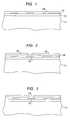
- a silicon substrate 11is shown partially cut away to indicate that is a portion of a much larger silicon wafer. It will be understood that these drawings are not to scale, and some features are shown exaggerated for convenience in this exposition.
- the silicon substrateis covered with a first oxide layer 12 , typically the field oxide, a metal interconnect level 13 , and an interlevel dielectric layer 14 , which is typically deposited oxide, or other suitable dielectric material.
- Low E organic materialssuch as xerogel or aerogel, are also suitable and can be applied using spin-on techniques. These elements are standard in silicon IC technology and form no part of the invention.
- Metal level 13should be taken as the next to last metal level, even though other levels are typically present but not shown.
- a photolithographic mask 16is applied to the dielectric layer 14 , and patterned to expose portions of the interlevel dielectric where interlevel interconnections are to be made. It will be understood that where photolithography or photomasks are mentioned in this description, other lithographic processes, such as x-ray or e-beam lithography, can be substituted.
- window 18is formed through the interlevel dielectric, as shown in FIG. 3, for interlevel interconnection to metal runner 15 .
- the interlevel window 18is plugged by depositing a suitable window plug material over the dielectric and into the window. For example, a dual layer of e.g. TiN and tungsten, represented by layers 21 and 22 in FIG.
- CMPchemical mechanical polishing
- any suitable process for forming the interlevel interconnectioncan be used.
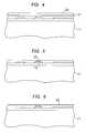
- an etch stop layer 25is then blanket deposited over the interlevel dielectric and interlevel windows as shown.
- a suitable etch stop layeris silicon nitride which withstands typical oxide etchant processes, e.g. RIE etch methods, and protects the interlevel plug when forming.
- the thickness of the etch stop layeris typically 500-1500 Angstroms.
- dielectric layer 31is deposited over the structure, and masked with lithographic mask 32 as shown in FIG. 8 .
- Mask 32is patterned to provide opening 33 to form an opening over the tungsten plug 23 .
- the exposed oxideis etched away, preferably using RIE, and the silicon nitride etch stop in window 33 is removed to leave the structure of FIG. 10 .
- a barrier layer 41is blanket deposited over the surface of the structure and into the window as shown.
- This layeris the first step in defining the copper interconnection layer which, in the sequence described here, is the last, or the top, metal layer in the IC, and is the layer to which wire bonds are to be made.
- Other copper metallization levelsmay also be present in structure, but the invention pertains to the last metal level to which interconnection is made by wire bonding.
- the preferred material for barrier layer 41is Ta, TaN, Ti, or TiN, although other materials may be used.
- the barrier layercan be deposited by chemical vapor deposition (CVD) or physical vapor deposition (PVD). A 100-1000 Angstrom layer is suitable.
- a copper strike layer 42is then blanket deposited by PVD.
- the thickness of the copper strike layermay be just sufficient to provide a seed layer over the surface for blanket electrolytic deposition, e.g. 1000-2000 Angstroms.
- the copper seed layer 42enables electrolytic deposition, by standard techniques, of copper layer 43 .
- the thickness of layer 43should be sufficient to completely plug the opening 33 (FIG. 12) as shown in FIG. 13, and is preferably 1.2-1.6 times the height of the opening.
- the surfaceis planarized using CMP in the manner described before, to produce the structure shown in FIG. 14 with copper plug 44 surrounded on the sides and bottom by barrier layer 45 .
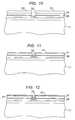
- barrier layer 51is blanket deposited over the structure as shown in FIG. 15 .
- This barrier layerhas essentially the same prescription as barrier layer 41 and ensures that all sides of the copper metallization layer are sealed to prevent copper migration in the IC.
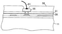
- Wire bond contactis then made to the copper metallization layer as shown in FIGS. 16-20.
- the thin barrier layer 51is covered with a thick layer of aluminum 52 .
- the aluminum layer 52may be deposited by CVD or PVD and has a thickness preferably in the range 0.2-1.0 ⁇ m.
- a lithographic mask 53is then applied to etch layers 51 and 52 to define the aluminum bonding pad, as shown in FIG. 17, and the unwanted portions of these layers are etches away using conventional techniques to produce the bonding pad 56 , separated from the copper plug by barrier layer 55 as shown in FIG. 18 .
- a conventional passivating layer 58is then applied to cap the IC.
- the capping layermay be Si 3 N 4 (SINCAPS) or may be a polymer such as polyimide.
- the capping layeris photodefinable polyimide.
- the capping layer 58is then patterned, if photodefinable, or masked and etched to form window 59 and expose the surface of aluminum bond pad 56 , as shown in FIG. 19 .
- Standard photoresist and etching techniquescan be used to pattern silicon nitride. If layer 58 is photodefinable polymer, the photoresist can be omitted and the layer itself patterned by exposure and development.
- wire 61is bonded to the aluminum pad 56 by thermocompression (TC) bonding.
- the wireis preferably gold, or a gold alloy with small amounts of metal additives, such as Au—Be, for hardening etc.
- the diameter of the wireis typically 0.5-2 mils, and preferably 1-1.2 mils.
- the area of the aluminum bond padsis typically in the range 1000-40000 ⁇ m 2 and preferably 5000-25000 ⁇ m 2 .
- the TC bonding operationis standard.
- the forcemay be 15-60 grams, preferably 40-60 grams.
- the ultrasonic frequencyis in the range 40-200 kHz, preferably 60-120 kHz, and the power in the range 20-200 mW, preferably 50-100 mW. These parameters are suitable for a variety of bonding tools including, e.g. K & S wire bonders.
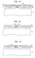
- FIGS. 21-24An alternative approach to the last few steps of the process described above is shown in FIGS. 21-24.
- the cap layer 72is applied prior to the aluminum bonding pad layer.
- window 71is shown in cap layer 72 .
- Window 71exposes the copper metallization 44 .
- Barrier layer 73 and aluminum layer 74are blanket deposited over the cap layer 72 , as shown in FIG. 22 and into the window to contact the copper metallization layer.
- Aluminum layer 74is then masked with mask 76 , as shown in FIG. 22, and layers 74 and then 73 are etched to form aluminum bond pad 77 in FIG. 23 .
- the maskis removed and the gold TC wire bond 78 applied to complete the interconnection.
- the last metal patternis copper
- the barrier layers as describedare intended to isolate the copper and prevent migration into regions of different metallurgy below.
- the underlying levelsare also comprise copper metallization the last level, the level shown in the Figures, need not have the barriers shown between metallization levels. It is still important in any case that an effective barrier be present between the last copper bonding region and the aluminum wire bonding pad.
- III-V photonic integrated circuitstypically have GaAs or InP substrates and multilevels of III-V ternary and/or quaternary layers forming the active devices.
- interconnectionscan in some applications be similar to those used in silicon IC technology.
- circuitsalso typically operate at very high speeds where copper metallization is distinctly advantageous.
- first level metalis typically polysilicon to form the gates and form interconnections for those gates.
- the metal interconnect levels formed after the first levelare usually aluminum, and one to three aluminum levels are typical. Of these one or more, will be substituted with copper according to the teachings described above. At least one of the copper levels has wire bonding sites which are converted to aluminum bonding sites according to the invention.
- Reference to a first metallization level or a second metallization levelshould be understood to refer to the first or second levels recited, not necessarily to the first or second levels in the IC structure.
Landscapes
- Engineering & Computer Science (AREA)
- Computer Hardware Design (AREA)
- Microelectronics & Electronic Packaging (AREA)
- Power Engineering (AREA)
- Manufacturing & Machinery (AREA)
- Physics & Mathematics (AREA)
- Condensed Matter Physics & Semiconductors (AREA)
- General Physics & Mathematics (AREA)
- Internal Circuitry In Semiconductor Integrated Circuit Devices (AREA)
- Wire Bonding (AREA)
Abstract
Description
Claims (3)
Priority Applications (1)
| Application Number | Priority Date | Filing Date | Title |
|---|---|---|---|
| US09/864,577US6472304B2 (en) | 1999-01-23 | 2001-05-24 | Wire bonding to copper |
Applications Claiming Priority (2)
| Application Number | Priority Date | Filing Date | Title |
|---|---|---|---|
| US23640699A | 1999-01-23 | 1999-01-23 | |
| US09/864,577US6472304B2 (en) | 1999-01-23 | 2001-05-24 | Wire bonding to copper |
Related Parent Applications (1)
| Application Number | Title | Priority Date | Filing Date |
|---|---|---|---|
| US23640699AContinuation | 1999-01-23 | 1999-01-23 |
Publications (2)
| Publication Number | Publication Date |
|---|---|
| US20010036716A1 US20010036716A1 (en) | 2001-11-01 |
| US6472304B2true US6472304B2 (en) | 2002-10-29 |
Family
ID=22889365
Family Applications (1)
| Application Number | Title | Priority Date | Filing Date |
|---|---|---|---|
| US09/864,577Expired - LifetimeUS6472304B2 (en) | 1999-01-23 | 2001-05-24 | Wire bonding to copper |
Country Status (6)
| Country | Link |
|---|---|
| US (1) | US6472304B2 (en) |
| EP (1) | EP1022776B1 (en) |
| JP (1) | JP3575676B2 (en) |
| KR (1) | KR100659801B1 (en) |
| DE (1) | DE60039800D1 (en) |
| TW (1) | TW426980B (en) |
Cited By (14)
| Publication number | Priority date | Publication date | Assignee | Title |
|---|---|---|---|---|
| US20010026952A1 (en)* | 1998-09-23 | 2001-10-04 | Manfred Engelhardt | Integrated circuit configuration and production method |
| US20050098605A1 (en)* | 2003-11-06 | 2005-05-12 | International Business Machines Corporation | Apparatus and method for low pressure wirebond |
| US20050258484A1 (en)* | 2004-05-20 | 2005-11-24 | Denso Corporation | Power composite integrated semiconductor device and manufacturing method thereof |
| US20060063365A1 (en)* | 2004-09-23 | 2006-03-23 | Wang Chung Y | Aluminum cap for reducing scratch and wire-bond bridging of bond pads |
| US20070026631A1 (en)* | 2005-07-29 | 2007-02-01 | Mou-Shiung Lin | Metal pad or metal bump over pad exposed by passivation layer |
| US20070023919A1 (en)* | 2005-07-29 | 2007-02-01 | Mou-Shiung Lin | Bonding pad on ic substrate and method for making the same |
| US20070102812A1 (en)* | 2005-11-08 | 2007-05-10 | Lsi Logic Corporation | Reduction of macro level stresses in copper/Low-K wafers by altering aluminum pad/passivation stack to reduce or eliminate IMC cracking in post wire bonded dies |
| US20080008823A1 (en)* | 2003-01-07 | 2008-01-10 | Ling Chen | Deposition processes for tungsten-containing barrier layers |
| US20090057907A1 (en)* | 2007-08-30 | 2009-03-05 | Ming-Tzong Yang | Interconnection structure |
| US20090152725A1 (en)* | 2007-12-14 | 2009-06-18 | Ami Semiconductor, Inc. | Thick metal interconnect with metal pad caps at selective sites and process for making the same |
| US20110079907A1 (en)* | 2009-10-05 | 2011-04-07 | International Business Machines Corporation | Semiconductor device having a copper plug |
| US9831122B2 (en) | 2012-05-29 | 2017-11-28 | Globalfoundries Inc. | Integrated circuit including wire structure, related method and design structure |
| US10115688B2 (en)* | 2015-05-29 | 2018-10-30 | Infineon Technologies Ag | Solder metallization stack and methods of formation thereof |
| US11804459B2 (en) | 2020-01-31 | 2023-10-31 | Samsung Electronics Co., Ltd. | Semiconductor device and method of fabricating the same |
Families Citing this family (15)
| Publication number | Priority date | Publication date | Assignee | Title |
|---|---|---|---|---|
| US6303423B1 (en) | 1998-12-21 | 2001-10-16 | Megic Corporation | Method for forming high performance system-on-chip using post passivation process |
| US6790757B1 (en) | 1999-12-20 | 2004-09-14 | Agere Systems Inc. | Wire bonding method for copper interconnects in semiconductor devices |
| JP2002076051A (en)* | 2000-09-01 | 2002-03-15 | Nec Corp | Bonding pad structure and bonding method of semiconductor device |
| EP1119046A3 (en)* | 2000-01-21 | 2002-07-03 | Lucent Technologies Inc. | Wire bonding technique and architecture suitable for copper metallization in semiconductor structures |
| JP3651765B2 (en)* | 2000-03-27 | 2005-05-25 | 株式会社東芝 | Semiconductor device |
| KR20020006779A (en)* | 2000-07-13 | 2002-01-26 | 박종섭 | Manufacturing method for metal line in semiconductor device |
| KR100374300B1 (en)* | 2000-10-06 | 2003-03-03 | 동부전자 주식회사 | Copper layer for semiconductor fabrication method |
| JP2003031575A (en)* | 2001-07-17 | 2003-01-31 | Nec Corp | Semiconductor device and manufacturing method thereof |
| US6683383B2 (en)* | 2001-10-18 | 2004-01-27 | Intel Corporation | Wirebond structure and method to connect to a microelectronic die |
| US6949461B2 (en)* | 2002-12-11 | 2005-09-27 | International Business Machines Corporation | Method for depositing a metal layer on a semiconductor interconnect structure |
| US7566964B2 (en)* | 2003-04-10 | 2009-07-28 | Agere Systems Inc. | Aluminum pad power bus and signal routing for integrated circuit devices utilizing copper technology interconnect structures |
| US8384189B2 (en) | 2005-03-29 | 2013-02-26 | Megica Corporation | High performance system-on-chip using post passivation process |
| JP2008066451A (en)* | 2006-09-06 | 2008-03-21 | Rohm Co Ltd | Semiconductor device |
| US20150212357A1 (en)* | 2014-01-24 | 2015-07-30 | Himax Display, Inc. | Manufacturing process for liquid crystal display panel |
| US9761548B1 (en)* | 2016-05-19 | 2017-09-12 | Infineon Technologies Ag | Bond pad structure |
Citations (9)
| Publication number | Priority date | Publication date | Assignee | Title |
|---|---|---|---|---|
| US3733685A (en)* | 1968-11-25 | 1973-05-22 | Gen Motors Corp | Method of making a passivated wire bonded semiconductor device |
| JPS5982737A (en)* | 1982-11-04 | 1984-05-12 | Nippon Telegr & Teleph Corp <Ntt> | Structure of electrode section of semiconductor device and its manufacture |
| JPS63128634A (en)* | 1986-11-18 | 1988-06-01 | Nec Corp | Manufacture of semiconductor device |
| US4845543A (en)* | 1983-09-28 | 1989-07-04 | Hitachi, Ltd. | Semiconductor device and method of manufacturing the same |
| US4933305A (en)* | 1987-07-31 | 1990-06-12 | Nec Corporation | Process of wire bonding for semiconductor device |
| US5968333A (en)* | 1998-04-07 | 1999-10-19 | Advanced Micro Devices, Inc. | Method of electroplating a copper or copper alloy interconnect |
| US6069068A (en)* | 1997-05-30 | 2000-05-30 | International Business Machines Corporation | Sub-quarter-micron copper interconnections with improved electromigration resistance and reduced defect sensitivity |
| US6117769A (en)* | 1998-08-11 | 2000-09-12 | Advanced Micro Devices, Inc. | Pad structure for copper interconnection and its formation |
| US6197688B1 (en)* | 1998-02-12 | 2001-03-06 | Motorola Inc. | Interconnect structure in a semiconductor device and method of formation |
Family Cites Families (6)
| Publication number | Priority date | Publication date | Assignee | Title |
|---|---|---|---|---|
| JP2563652B2 (en)* | 1990-07-17 | 1996-12-11 | 株式会社東芝 | Semiconductor device and manufacturing method thereof |
| JPH0567686A (en)* | 1991-09-09 | 1993-03-19 | Hitachi Ltd | Semiconductor device wiring |
| JPH0878410A (en)* | 1994-09-05 | 1996-03-22 | Mitsubishi Electric Corp | Wiring connection part and manufacturing method thereof |
| US5661081A (en)* | 1994-09-30 | 1997-08-26 | United Microelectronics Corporation | Method of bonding an aluminum wire to an intergrated circuit bond pad |
| US6537905B1 (en)* | 1996-12-30 | 2003-03-25 | Applied Materials, Inc. | Fully planarized dual damascene metallization using copper line interconnect and selective CVD aluminum plug |
| JP3906522B2 (en)* | 1997-06-10 | 2007-04-18 | ソニー株式会社 | Manufacturing method of semiconductor device |
- 1999
- 1999-11-24TWTW088120537Apatent/TW426980B/ennot_activeIP Right Cessation
- 2000
- 2000-01-13DEDE60039800Tpatent/DE60039800D1/ennot_activeExpired - Lifetime
- 2000-01-13EPEP00300208Apatent/EP1022776B1/ennot_activeExpired - Lifetime
- 2000-01-17JPJP2000007951Apatent/JP3575676B2/ennot_activeExpired - Lifetime
- 2000-01-22KRKR1020000003060Apatent/KR100659801B1/ennot_activeExpired - Lifetime
- 2001
- 2001-05-24USUS09/864,577patent/US6472304B2/ennot_activeExpired - Lifetime
Patent Citations (9)
| Publication number | Priority date | Publication date | Assignee | Title |
|---|---|---|---|---|
| US3733685A (en)* | 1968-11-25 | 1973-05-22 | Gen Motors Corp | Method of making a passivated wire bonded semiconductor device |
| JPS5982737A (en)* | 1982-11-04 | 1984-05-12 | Nippon Telegr & Teleph Corp <Ntt> | Structure of electrode section of semiconductor device and its manufacture |
| US4845543A (en)* | 1983-09-28 | 1989-07-04 | Hitachi, Ltd. | Semiconductor device and method of manufacturing the same |
| JPS63128634A (en)* | 1986-11-18 | 1988-06-01 | Nec Corp | Manufacture of semiconductor device |
| US4933305A (en)* | 1987-07-31 | 1990-06-12 | Nec Corporation | Process of wire bonding for semiconductor device |
| US6069068A (en)* | 1997-05-30 | 2000-05-30 | International Business Machines Corporation | Sub-quarter-micron copper interconnections with improved electromigration resistance and reduced defect sensitivity |
| US6197688B1 (en)* | 1998-02-12 | 2001-03-06 | Motorola Inc. | Interconnect structure in a semiconductor device and method of formation |
| US5968333A (en)* | 1998-04-07 | 1999-10-19 | Advanced Micro Devices, Inc. | Method of electroplating a copper or copper alloy interconnect |
| US6117769A (en)* | 1998-08-11 | 2000-09-12 | Advanced Micro Devices, Inc. | Pad structure for copper interconnection and its formation |
Cited By (35)
| Publication number | Priority date | Publication date | Assignee | Title |
|---|---|---|---|---|
| US20010026952A1 (en)* | 1998-09-23 | 2001-10-04 | Manfred Engelhardt | Integrated circuit configuration and production method |
| US20040038507A1 (en)* | 1998-09-23 | 2004-02-26 | Infineon Technologies Ag | Method of producing an integrated circuit configuration |
| US6828680B2 (en)* | 1998-09-23 | 2004-12-07 | Infineon Technologies Ag | Integrated circuit configuration using spacers as a diffusion barrier and method of producing such an integrated circuit configuration |
| US6998338B2 (en) | 1998-09-23 | 2006-02-14 | Infineon Technologies Ag | Method of producing an integrated circuit configuration |
| US20080008823A1 (en)* | 2003-01-07 | 2008-01-10 | Ling Chen | Deposition processes for tungsten-containing barrier layers |
| US7507660B2 (en)* | 2003-01-07 | 2009-03-24 | Applied Materials, Inc. | Deposition processes for tungsten-containing barrier layers |
| US20050098605A1 (en)* | 2003-11-06 | 2005-05-12 | International Business Machines Corporation | Apparatus and method for low pressure wirebond |
| US7691697B2 (en) | 2004-05-20 | 2010-04-06 | Denso Corporation | Power composite integrated semiconductor device and manufacturing method thereof |
| US7235844B2 (en) | 2004-05-20 | 2007-06-26 | Denso Corporation | Power composite integrated semiconductor device and manufacturing method thereof |
| US20070187841A1 (en)* | 2004-05-20 | 2007-08-16 | Denso Corporation | Power composite integrated semiconductor device and manufacturing method thereof |
| US20050258484A1 (en)* | 2004-05-20 | 2005-11-24 | Denso Corporation | Power composite integrated semiconductor device and manufacturing method thereof |
| US7416932B2 (en) | 2004-05-20 | 2008-08-26 | Denso Corporation | Power composite integrated semiconductor device and manufacturing method thereof |
| US20080311740A1 (en)* | 2004-05-20 | 2008-12-18 | Denso Corporation | Power composite integrated semiconductor device and manufacturing method thereof |
| US7833896B2 (en) | 2004-09-23 | 2010-11-16 | Taiwan Semiconductor Manufacturing Company, Ltd. | Aluminum cap for reducing scratch and wire-bond bridging of bond pads |
| US20060063365A1 (en)* | 2004-09-23 | 2006-03-23 | Wang Chung Y | Aluminum cap for reducing scratch and wire-bond bridging of bond pads |
| US20070023919A1 (en)* | 2005-07-29 | 2007-02-01 | Mou-Shiung Lin | Bonding pad on ic substrate and method for making the same |
| US8399989B2 (en) | 2005-07-29 | 2013-03-19 | Megica Corporation | Metal pad or metal bump over pad exposed by passivation layer |
| US8148822B2 (en) | 2005-07-29 | 2012-04-03 | Megica Corporation | Bonding pad on IC substrate and method for making the same |
| US20070026631A1 (en)* | 2005-07-29 | 2007-02-01 | Mou-Shiung Lin | Metal pad or metal bump over pad exposed by passivation layer |
| US8076779B2 (en)* | 2005-11-08 | 2011-12-13 | Lsi Corporation | Reduction of macro level stresses in copper/low-K wafers |
| US20070102812A1 (en)* | 2005-11-08 | 2007-05-10 | Lsi Logic Corporation | Reduction of macro level stresses in copper/Low-K wafers by altering aluminum pad/passivation stack to reduce or eliminate IMC cracking in post wire bonded dies |
| US20090057907A1 (en)* | 2007-08-30 | 2009-03-05 | Ming-Tzong Yang | Interconnection structure |
| US7800239B2 (en) | 2007-12-14 | 2010-09-21 | Semiconductor Components Industries, Llc | Thick metal interconnect with metal pad caps at selective sites and process for making the same |
| US7947592B2 (en) | 2007-12-14 | 2011-05-24 | Semiconductor Components Industries, Llc | Thick metal interconnect with metal pad caps at selective sites and process for making the same |
| US20090152100A1 (en)* | 2007-12-14 | 2009-06-18 | Ami Semiconductor, Inc. | Thick metal interconnect with metal pad caps at selective sites and process for making the same |
| US20090152725A1 (en)* | 2007-12-14 | 2009-06-18 | Ami Semiconductor, Inc. | Thick metal interconnect with metal pad caps at selective sites and process for making the same |
| US20110079907A1 (en)* | 2009-10-05 | 2011-04-07 | International Business Machines Corporation | Semiconductor device having a copper plug |
| US8610283B2 (en)* | 2009-10-05 | 2013-12-17 | International Business Machines Corporation | Semiconductor device having a copper plug |
| US8922019B2 (en) | 2009-10-05 | 2014-12-30 | International Business Machines Corporation | Semiconductor device having a copper plug |
| US9831122B2 (en) | 2012-05-29 | 2017-11-28 | Globalfoundries Inc. | Integrated circuit including wire structure, related method and design structure |
| US10224276B2 (en) | 2012-05-29 | 2019-03-05 | Globalfoundries Inc. | Integrated circuit including wire structure, related method and design structure |
| US10115688B2 (en)* | 2015-05-29 | 2018-10-30 | Infineon Technologies Ag | Solder metallization stack and methods of formation thereof |
| US10573611B2 (en) | 2015-05-29 | 2020-02-25 | Infineon Technologies Ag | Solder metallization stack and methods of formation thereof |
| US11804459B2 (en) | 2020-01-31 | 2023-10-31 | Samsung Electronics Co., Ltd. | Semiconductor device and method of fabricating the same |
| US12142587B2 (en) | 2020-01-31 | 2024-11-12 | Samsung Electronics Co., Ltd. | Semiconductor device and method of fabricating the same |
Also Published As
| Publication number | Publication date |
|---|---|
| EP1022776A3 (en) | 2000-09-13 |
| KR100659801B1 (en) | 2006-12-19 |
| US20010036716A1 (en) | 2001-11-01 |
| DE60039800D1 (en) | 2008-09-25 |
| KR20000057792A (en) | 2000-09-25 |
| TW426980B (en) | 2001-03-21 |
| EP1022776B1 (en) | 2008-08-13 |
| EP1022776A2 (en) | 2000-07-26 |
| JP3575676B2 (en) | 2004-10-13 |
| JP2000216191A (en) | 2000-08-04 |
Similar Documents
| Publication | Publication Date | Title |
|---|---|---|
| US6472304B2 (en) | Wire bonding to copper | |
| US6333559B1 (en) | Method/structure for creating aluminum wirebound pad on copper BEOL | |
| US7829452B2 (en) | Terminal pad structures and methods of fabricating same | |
| US6730982B2 (en) | FBEOL process for Cu metallizations free from Al-wirebond pads | |
| US6344410B1 (en) | Manufacturing method for semiconductor metalization barrier | |
| US7777300B2 (en) | Semiconductor device with capacitor | |
| US8581366B2 (en) | Method and system for forming conductive bumping with copper interconnection | |
| US7816792B2 (en) | Semiconductor device with conductive interconnect | |
| US20090072393A1 (en) | Structure and Method for Fabricating Flip Chip Devices | |
| US7566964B2 (en) | Aluminum pad power bus and signal routing for integrated circuit devices utilizing copper technology interconnect structures | |
| KR100691051B1 (en) | Semiconductor Device and Bond Pad Formation Process | |
| US6987057B2 (en) | Method making bonding pad | |
| US6346472B1 (en) | Manufacturing method for semiconductor metalization barrier | |
| US7245025B2 (en) | Low cost bonding pad and method of fabricating same | |
| US20020068385A1 (en) | Method for forming anchored bond pads in semiconductor devices and devices formed | |
| WO2010049087A2 (en) | A semiconductor device including a reduced stress configuration for metal pillars | |
| US20240312857A1 (en) | Semiconductor structure and method of fabricating same | |
| WO2005062367A1 (en) | I/o sites for probe test and wire bond | |
| US20240038719A1 (en) | Novel method of forming wafer-to-wafer bonding structure | |
| EP1490906A1 (en) | Beol process for cu metallizations free from al-wirebond pads |
Legal Events
| Date | Code | Title | Description |
|---|---|---|---|
| STCF | Information on status: patent grant | Free format text:PATENTED CASE | |
| FPAY | Fee payment | Year of fee payment:4 | |
| FPAY | Fee payment | Year of fee payment:8 | |
| FPAY | Fee payment | Year of fee payment:12 | |
| AS | Assignment | Owner name:DEUTSCHE BANK AG NEW YORK BRANCH, AS COLLATERAL AG Free format text:PATENT SECURITY AGREEMENT;ASSIGNORS:LSI CORPORATION;AGERE SYSTEMS LLC;REEL/FRAME:032856/0031 Effective date:20140506 | |
| AS | Assignment | Owner name:AVAGO TECHNOLOGIES GENERAL IP (SINGAPORE) PTE. LTD Free format text:ASSIGNMENT OF ASSIGNORS INTEREST;ASSIGNOR:AGERE SYSTEMS LLC;REEL/FRAME:035059/0001 Effective date:20140804 Owner name:AGERE SYSTEMS LLC, PENNSYLVANIA Free format text:MERGER;ASSIGNOR:AGERE SYSTEMS INC.;REEL/FRAME:035058/0895 Effective date:20120724 | |
| AS | Assignment | Owner name:LSI CORPORATION, CALIFORNIA Free format text:TERMINATION AND RELEASE OF SECURITY INTEREST IN PATENT RIGHTS (RELEASES RF 032856-0031);ASSIGNOR:DEUTSCHE BANK AG NEW YORK BRANCH, AS COLLATERAL AGENT;REEL/FRAME:037684/0039 Effective date:20160201 Owner name:AGERE SYSTEMS LLC, PENNSYLVANIA Free format text:TERMINATION AND RELEASE OF SECURITY INTEREST IN PATENT RIGHTS (RELEASES RF 032856-0031);ASSIGNOR:DEUTSCHE BANK AG NEW YORK BRANCH, AS COLLATERAL AGENT;REEL/FRAME:037684/0039 Effective date:20160201 | |
| AS | Assignment | Owner name:BANK OF AMERICA, N.A., AS COLLATERAL AGENT, NORTH CAROLINA Free format text:PATENT SECURITY AGREEMENT;ASSIGNOR:AVAGO TECHNOLOGIES GENERAL IP (SINGAPORE) PTE. LTD.;REEL/FRAME:037808/0001 Effective date:20160201 Owner name:BANK OF AMERICA, N.A., AS COLLATERAL AGENT, NORTH Free format text:PATENT SECURITY AGREEMENT;ASSIGNOR:AVAGO TECHNOLOGIES GENERAL IP (SINGAPORE) PTE. LTD.;REEL/FRAME:037808/0001 Effective date:20160201 | |
| AS | Assignment | Owner name:AVAGO TECHNOLOGIES GENERAL IP (SINGAPORE) PTE. LTD., SINGAPORE Free format text:TERMINATION AND RELEASE OF SECURITY INTEREST IN PATENTS;ASSIGNOR:BANK OF AMERICA, N.A., AS COLLATERAL AGENT;REEL/FRAME:041710/0001 Effective date:20170119 Owner name:AVAGO TECHNOLOGIES GENERAL IP (SINGAPORE) PTE. LTD Free format text:TERMINATION AND RELEASE OF SECURITY INTEREST IN PATENTS;ASSIGNOR:BANK OF AMERICA, N.A., AS COLLATERAL AGENT;REEL/FRAME:041710/0001 Effective date:20170119 | |
| AS | Assignment | Owner name:AGERE SYSTEMS INC., PENNSYLVANIA Free format text:MERGER AND CHANGE OF NAME;ASSIGNORS:AGERE SYSTEMS GUARDIAN CORP.;AGERE SYSTEMS INC.;REEL/FRAME:044416/0779 Effective date:20020822 Owner name:AGERE SYSTEMS GUARDIAN CORP., PENNSYLVANIA Free format text:ASSIGNMENT OF ASSIGNORS INTEREST;ASSIGNOR:LUCENT TECHNOLOGIES, INC.;REEL/FRAME:044780/0092 Effective date:20010130 | |
| AS | Assignment | Owner name:BELL SEMICONDUCTOR, LLC, ILLINOIS Free format text:ASSIGNMENT OF ASSIGNORS INTEREST;ASSIGNORS:AVAGO TECHNOLOGIES GENERAL IP (SINGAPORE) PTE. LTD.;BROADCOM CORPORATION;REEL/FRAME:044415/0144 Effective date:20171208 Owner name:BELL SEMICONDUCTOR, LLC, ILLINOIS Free format text:ASSIGNMENT OF ASSIGNORS INTEREST;ASSIGNORS:AVAGO TECHNOLOGIES GENERAL IP (SINGAPORE) PTE. LTD.;BROADCOM CORPORATION;REEL/FRAME:044886/0766 Effective date:20171208 | |
| AS | Assignment | Owner name:CORTLAND CAPITAL MARKET SERVICES LLC, AS COLLATERA Free format text:SECURITY INTEREST;ASSIGNORS:HILCO PATENT ACQUISITION 56, LLC;BELL SEMICONDUCTOR, LLC;BELL NORTHERN RESEARCH, LLC;REEL/FRAME:045216/0020 Effective date:20180124 | |
| AS | Assignment | Owner name:BELL NORTHERN RESEARCH, LLC, ILLINOIS Free format text:RELEASE BY SECURED PARTY;ASSIGNOR:CORTLAND CAPITAL MARKET SERVICES LLC;REEL/FRAME:059723/0382 Effective date:20220401 Owner name:BELL SEMICONDUCTOR, LLC, ILLINOIS Free format text:RELEASE BY SECURED PARTY;ASSIGNOR:CORTLAND CAPITAL MARKET SERVICES LLC;REEL/FRAME:059723/0382 Effective date:20220401 Owner name:HILCO PATENT ACQUISITION 56, LLC, ILLINOIS Free format text:RELEASE BY SECURED PARTY;ASSIGNOR:CORTLAND CAPITAL MARKET SERVICES LLC;REEL/FRAME:059723/0382 Effective date:20220401 Owner name:BELL NORTHERN RESEARCH, LLC, ILLINOIS Free format text:RELEASE BY SECURED PARTY;ASSIGNOR:CORTLAND CAPITAL MARKET SERVICES LLC;REEL/FRAME:059720/0001 Effective date:20220401 Owner name:BELL SEMICONDUCTOR, LLC, ILLINOIS Free format text:RELEASE BY SECURED PARTY;ASSIGNOR:CORTLAND CAPITAL MARKET SERVICES LLC;REEL/FRAME:059720/0001 Effective date:20220401 Owner name:HILCO PATENT ACQUISITION 56, LLC, ILLINOIS Free format text:RELEASE BY SECURED PARTY;ASSIGNOR:CORTLAND CAPITAL MARKET SERVICES LLC;REEL/FRAME:059720/0001 Effective date:20220401 |