US6472107B1 - Disposable hard mask for photomask plasma etching - Google Patents
Disposable hard mask for photomask plasma etchingDownload PDFInfo
- Publication number
- US6472107B1 US6472107B1US09/409,454US40945499AUS6472107B1US 6472107 B1US6472107 B1US 6472107B1US 40945499 AUS40945499 AUS 40945499AUS 6472107 B1US6472107 B1US 6472107B1
- Authority
- US
- United States
- Prior art keywords
- hard mask
- layer
- mask layer
- photomask
- photosensitive resist
- Prior art date
- Legal status (The legal status is an assumption and is not a legal conclusion. Google has not performed a legal analysis and makes no representation as to the accuracy of the status listed.)
- Expired - Lifetime
Links
- 238000001020plasma etchingMethods0.000titledescription4
- 239000000463materialSubstances0.000claimsabstractdescription125
- 238000000034methodMethods0.000claimsabstractdescription53
- 230000003667anti-reflective effectEffects0.000claimsabstractdescription49
- 238000005530etchingMethods0.000claimsabstractdescription30
- 239000007789gasSubstances0.000claimsdescription28
- VYPSYNLAJGMNEJ-UHFFFAOYSA-NSilicium dioxideChemical compoundO=[Si]=OVYPSYNLAJGMNEJ-UHFFFAOYSA-N0.000claimsdescription22
- 239000000758substrateSubstances0.000claimsdescription17
- 239000000203mixtureSubstances0.000claimsdescription12
- KZBUYRJDOAKODT-UHFFFAOYSA-NChlorineChemical compoundClClKZBUYRJDOAKODT-UHFFFAOYSA-N0.000claimsdescription11
- ZAMOUSCENKQFHK-UHFFFAOYSA-NChlorine atomChemical compound[Cl]ZAMOUSCENKQFHK-UHFFFAOYSA-N0.000claimsdescription11
- 239000000460chlorineSubstances0.000claimsdescription11
- 229910052801chlorineInorganic materials0.000claimsdescription11
- XPDWGBQVDMORPB-UHFFFAOYSA-NFluoroformChemical compoundFC(F)FXPDWGBQVDMORPB-UHFFFAOYSA-N0.000claimsdescription7
- CPELXLSAUQHCOX-UHFFFAOYSA-NHydrogen bromideChemical compoundBrCPELXLSAUQHCOX-UHFFFAOYSA-N0.000claimsdescription7
- WMIYKQLTONQJES-UHFFFAOYSA-NhexafluoroethaneChemical compoundFC(F)(F)C(F)(F)FWMIYKQLTONQJES-UHFFFAOYSA-N0.000claimsdescription7
- SFZCNBIFKDRMGX-UHFFFAOYSA-Nsulfur hexafluorideChemical compoundFS(F)(F)(F)(F)FSFZCNBIFKDRMGX-UHFFFAOYSA-N0.000claimsdescription7
- WKBOTKDWSSQWDR-UHFFFAOYSA-NBromine atomChemical compound[Br]WKBOTKDWSSQWDR-UHFFFAOYSA-N0.000claimsdescription5
- PXGOKWXKJXAPGV-UHFFFAOYSA-NFluorineChemical compoundFFPXGOKWXKJXAPGV-UHFFFAOYSA-N0.000claimsdescription5
- GDTBXPJZTBHREO-UHFFFAOYSA-NbromineSubstancesBrBrGDTBXPJZTBHREO-UHFFFAOYSA-N0.000claimsdescription5
- 229910052794bromiumInorganic materials0.000claimsdescription5
- 229910052681coesiteInorganic materials0.000claimsdescription5
- 229910052906cristobaliteInorganic materials0.000claimsdescription5
- 239000011737fluorineSubstances0.000claimsdescription5
- 229910052731fluorineInorganic materials0.000claimsdescription5
- 150000004820halidesChemical class0.000claimsdescription5
- 239000000377silicon dioxideSubstances0.000claimsdescription5
- 229910052682stishoviteInorganic materials0.000claimsdescription5
- 229910052905tridymiteInorganic materials0.000claimsdescription5
- 229910052581Si3N4Inorganic materials0.000claimsdescription4
- ATJFFYVFTNAWJD-UHFFFAOYSA-NTinChemical compound[Sn]ATJFFYVFTNAWJD-UHFFFAOYSA-N0.000claimsdescription4
- 239000011521glassSubstances0.000claimsdescription4
- 229910052718tinInorganic materials0.000claimsdescription4
- 238000004519manufacturing processMethods0.000abstractdescription3
- QDOXWKRWXJOMAK-UHFFFAOYSA-Ndichromium trioxideChemical compoundO=[Cr]O[Cr]=OQDOXWKRWXJOMAK-UHFFFAOYSA-N0.000description42
- 239000010453quartzSubstances0.000description12
- 239000004065semiconductorSubstances0.000description9
- QVGXLLKOCUKJST-UHFFFAOYSA-Natomic oxygenChemical compound[O]QVGXLLKOCUKJST-UHFFFAOYSA-N0.000description8
- 229910052760oxygenInorganic materials0.000description8
- 239000001301oxygenSubstances0.000description8
- 238000006243chemical reactionMethods0.000description5
- -1chrome radical speciesChemical class0.000description5
- 229910052710siliconInorganic materials0.000description5
- 238000001312dry etchingMethods0.000description4
- 230000005684electric fieldEffects0.000description4
- 239000010703siliconSubstances0.000description4
- XUIMIQQOPSSXEZ-UHFFFAOYSA-NSiliconChemical compound[Si]XUIMIQQOPSSXEZ-UHFFFAOYSA-N0.000description3
- 230000000694effectsEffects0.000description3
- 238000001039wet etchingMethods0.000description3
- VYZAMTAEIAYCRO-UHFFFAOYSA-NChromiumChemical compound[Cr]VYZAMTAEIAYCRO-UHFFFAOYSA-N0.000description2
- 238000005229chemical vapour depositionMethods0.000description2
- 150000002500ionsChemical class0.000description2
- 238000001459lithographyMethods0.000description2
- 238000005259measurementMethods0.000description2
- JBRZTFJDHDCESZ-UHFFFAOYSA-NAsGaChemical compound[As]#[Ga]JBRZTFJDHDCESZ-UHFFFAOYSA-N0.000description1
- 239000004215Carbon black (E152)Substances0.000description1
- 229910001218Gallium arsenideInorganic materials0.000description1
- 239000002253acidSubstances0.000description1
- 238000013459approachMethods0.000description1
- 230000015556catabolic processEffects0.000description1
- 238000006731degradation reactionMethods0.000description1
- 230000001419dependent effectEffects0.000description1
- 238000010894electron beam technologyMethods0.000description1
- 229930195733hydrocarbonNatural products0.000description1
- 150000002430hydrocarbonsChemical class0.000description1
- 238000010849ion bombardmentMethods0.000description1
- 239000007788liquidSubstances0.000description1
- 238000012986modificationMethods0.000description1
- 230000004048modificationEffects0.000description1
- 230000010363phase shiftEffects0.000description1
- 229920000642polymerPolymers0.000description1
- 238000004544sputter depositionMethods0.000description1
- 238000012546transferMethods0.000description1
Images


Classifications
- G—PHYSICS
- G03—PHOTOGRAPHY; CINEMATOGRAPHY; ANALOGOUS TECHNIQUES USING WAVES OTHER THAN OPTICAL WAVES; ELECTROGRAPHY; HOLOGRAPHY
- G03F—PHOTOMECHANICAL PRODUCTION OF TEXTURED OR PATTERNED SURFACES, e.g. FOR PRINTING, FOR PROCESSING OF SEMICONDUCTOR DEVICES; MATERIALS THEREFOR; ORIGINALS THEREFOR; APPARATUS SPECIALLY ADAPTED THEREFOR
- G03F1/00—Originals for photomechanical production of textured or patterned surfaces, e.g., masks, photo-masks, reticles; Mask blanks or pellicles therefor; Containers specially adapted therefor; Preparation thereof
- G03F1/68—Preparation processes not covered by groups G03F1/20 - G03F1/50
- G03F1/76—Patterning of masks by imaging
- G—PHYSICS
- G03—PHOTOGRAPHY; CINEMATOGRAPHY; ANALOGOUS TECHNIQUES USING WAVES OTHER THAN OPTICAL WAVES; ELECTROGRAPHY; HOLOGRAPHY
- G03F—PHOTOMECHANICAL PRODUCTION OF TEXTURED OR PATTERNED SURFACES, e.g. FOR PRINTING, FOR PROCESSING OF SEMICONDUCTOR DEVICES; MATERIALS THEREFOR; ORIGINALS THEREFOR; APPARATUS SPECIALLY ADAPTED THEREFOR
- G03F1/00—Originals for photomechanical production of textured or patterned surfaces, e.g., masks, photo-masks, reticles; Mask blanks or pellicles therefor; Containers specially adapted therefor; Preparation thereof
- G03F1/68—Preparation processes not covered by groups G03F1/20 - G03F1/50
- G03F1/80—Etching
- G—PHYSICS
- G03—PHOTOGRAPHY; CINEMATOGRAPHY; ANALOGOUS TECHNIQUES USING WAVES OTHER THAN OPTICAL WAVES; ELECTROGRAPHY; HOLOGRAPHY
- G03F—PHOTOMECHANICAL PRODUCTION OF TEXTURED OR PATTERNED SURFACES, e.g. FOR PRINTING, FOR PROCESSING OF SEMICONDUCTOR DEVICES; MATERIALS THEREFOR; ORIGINALS THEREFOR; APPARATUS SPECIALLY ADAPTED THEREFOR
- G03F7/00—Photomechanical, e.g. photolithographic, production of textured or patterned surfaces, e.g. printing surfaces; Materials therefor, e.g. comprising photoresists; Apparatus specially adapted therefor
- G03F7/004—Photosensitive materials
- G03F7/09—Photosensitive materials characterised by structural details, e.g. supports, auxiliary layers
- G03F7/094—Multilayer resist systems, e.g. planarising layers
Definitions
- the present inventionrelates to a photomask which includes a hard mask layer, the use of which improves the uniformity of critical dimensions on the photomask.
- Photomasksare used in the semiconductor industry to transfer micro-scale images defining a semiconductor circuit onto a silicon or gallium arsenide substrate or wafer.
- a typical binary photomaskis comprised of a transparent quartz substrate and chrome (Cr) opaque material that includes an integral layer of chrome oxide (CrO) anti-reflective (AR) material.
- Crchrome
- ARanti-reflective
- a photomaskis interposed between the semiconductor wafer, which includes a layer of photosensitive material, and an energy source commonly referred to as a Stepper.
- the energy generated by the Stepperpasses through the transparent portions of the quartz substrate not covered by the Cr opaque material and the CrO AR material, and causes a reaction in the photosensitive material on the semiconductor wafer.
- Energy from the Stepperis inhibited from passing through the areas of the photomask in which the Cr opaque material and CrO AR is present.
- the CrO AR materialprevents most, but not all, of the incident energy from being reflected back into the Stepper. If excess energy is reflected back into the Stepper a degraded image will be created in the photosensitive resist material on the semiconductor wafer surface, thereby resulting in a degradation of performance of the semiconductor device.
- a finished photomask used in the production of semiconductor devicesis formed from a “blank” or “undeveloped” photomask.
- a prior art blank photomask 20is comprised of four layers.
- the first layer 2is a layer of quartz, commonly referred to as the substrate, and is typically approximately one quarter inch thick.
- Affixed to the quartz substrate 2is a layer of Cr opaque material 4 which typically is approximately 900 ⁇ to 1000 ⁇ thick.
- An integral layer of CrO AR material 6is formed on top of the layer of Cr opaque material 4 .
- the layer of CrO AR materialis typically approximately 100 ⁇ thick.
- a layer of photosensitive resist material 8resides on top of the CrO AR material 6 .
- the photosensitive resist material 8is typically a hydrocarbon polymer, the various compositions and thicknesses of which are well known in the art.
- the desired pattern of Cr opaque material to be created on the photomaskmay be defined by an electronic data file loaded into an exposure system which typically scans an electron beam (E-beam) or laser beam in a raster fashion across the blank photomask.
- E-beamelectron beam
- the exposure systemdirects the E-beam or laser beam at addressable locations on the photomask as defined by the electronic data file.
- the areas of the photosensitive resist material that are exposed to the E-beam or laser beambecome soluble while the unexposed portions remain insoluble.
- the soluble photosensitive resistis removed by means well known in the art, and the unexposed, insoluble photosensitive resist material 10 remains adhered to the CrO AR material 6 .
- the exposed CrO AR material and the underlying Cr opaque material no longer covered by the photosensitive resist material in the prior art photomask 22is removed by a well known etching process, and only the portions of CrO AR material 12 and Cr opaque material 14 residing beneath the remaining photosensitive resist material 10 remain affixed to quartz substrate 2 .
- This initial or base etchingmay be accomplished by either a wet-etching or dry-etching process both of which are well known in the art.
- wet-etching processuses a liquid acid solution to erode away the exposed CrO AR material and Cr opaque material.
- a dry-etching processalso referred to as plasma etching, utilizes electrified gases, typically a mixture of chlorine and oxygen, to remove the exposed chrome oxide AR material and chrome opaque material.
- a dry-etching processis conducted in vacuum chamber in which gases, typically chlorine and oxygen are injected.
- gasestypically chlorine and oxygen are injected.
- An electrical fieldis created between an anode and a cathode in the vacuum chamber thereby forming a reactive gas plasma.
- Positive ions of the reactive gas plasmaare accelerated toward the photomask which is oriented such that the surface area of the quartz substrate is perpendicular to the electrical field.
- the directional ion bombardmentenhances the etch rate of the Cr opaque material and CrO AR material in the vertical direction but not in the horizontal direction (i.e., the etching is an isotropic or directional).
- the reaction between the reactive gas plasma and the Cr opaque material and CrO AR materialis a two step process. First, a reaction between the chlorine gas and exposed CrO AR material and Cr opaque material forms chrome radical species. The oxygen then reacts with the chrome radical species to create a volatile which can “boil off” thereby removing the exposed CrO AR material and the exposed Cr opaque material.
- the photosensitive resist material in the prior art photomask 24is stripped away by a process well known in the art.
- the dimensions of the Cr opaque material on the finished photomask 26are then measured to determine whether or not critical dimensions are within specified tolerances.
- Critical dimensionsmay be measured at a number of locations on the finished photomask, summed, and then divided by the number of measurements to obtain a numerical average of the critical dimensions. This obtained average is then compared to a specified target number (i.e., a mean to target comparison) to ensure compliance with predefined critical dimensions specifications.
- a specified target numberi.e., a mean to target comparison
- the etch rate of the plasma etching process described above(and hence the uniformity of the critical dimensions) is dependent on the desired pattern to be formed in the Cr opaque material and CrO AR material. In areas of the photomask where a substantial portion of Cr opaque material and CrO AR material are to be removed (i.e., macro loading), the etching process may take longer than in areas of the photomask in which small portions of Cr opaque material and CrO AR material are to be removed. Likewise, there may be differences in etch rate for micro loading conditions in which the etch rate is different between isolated and dense features in the same general area. These differing etch rates make it more difficult for the finished photomask to conform to a specified uniformity requirement. Additionally, the above described etching process can also cause variances in critical dimensions because the photosensitive resist material is not entirely impervious to the plasma gases.
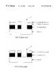
- FIG. 1is a cross-sectional view of a blank photomask illustrating the composition of the various layers of a typical prior art blank binary photomask.
- FIG. 2is a cross-sectional view of a prior art photomask after exposure to an energy source and having the soluble photosensitive material removed.
- FIG. 3is a cross-sectional view of a prior art binary photomask after being subjected to an etching process thereby removing the exposed CrO AR material and Cr opaque material.
- FIG. 4is a cross-sectional view of a finished, prior art binary photomask with the photosensitive material stripped away.
- FIG. 5is a cross-sectional view of a blank photomask is accordance with the instant invention illustrating the composition of the various layers of a typical blank photomask including a hard mask layer.
- FIG. 6is a cross-sectional view of a photomask in accordance with the instant invention after exposure to an energy source and having the soluble photosensitive material removed.
- FIG. 7is a cross-sectional view of a photomask in accordance with the instant invention after being subjected to a first etching process thereby removing the exposed hard mask material.
- FIG. 8is a cross-sectional view of a finished photomask in accordance with the first embodiment of the invention after being subjected to a second etching process thereby removing the exposed CrO AR material and Cr opaque material.
- FIG. 9is cross-sectional view of a second embodiment of a finished photomask is accordance with the present invention.
- FIG. 5depicts a blank photomask in accordance with the present invention.
- the blank photomask 30is comprised of a quartz substrate 2 having a thickness of approximately one quarter inch.
- a layer of Cr opaque material 4which is typically 900 ⁇ to 1000 ⁇ thick.
- An integral layer of CrO AR material 6is formed on top of the Cr opaque material 4 .
- Hard mask layer 18is deposited on top of the CrO AR material 6 .
- the hard mask layer 18may be deposited on the CrO AR layer using a sputtering process or any other method well known in the art such as chemical vapor deposition (CVD).
- CVDchemical vapor deposition
- the thickness of the hard mask layeris preferably in the range of 50 to 500 ⁇ , and is most preferably approximately 250 ⁇ thick.
- the hard mask layeris comprised of silicon (Si).
- the hard mask layermay also be comprised of other similar materials including but not limited to Ti, TiW, W, TiN, Si 3 N 4 , SiO 2 , or spin-on-glass.
- the process for creating a finished photomask, having improved critical dimensions and anti-reflective properties, from blank photomask 30is now described with reference to FIGS. 5 through 9.
- the desired pattern to be formed in the hard mask material 18 , the CrO AR material 6 , and the Cr opaque material 4is scanned onto the layer of photosensitive resist material 8 of blank photomask 30 by means of a raster scan exposure system, or comparable system (e.g., a vector scan tool).
- the portions of the photosensitive resist material that are exposed to the E-beam or laser beambecome soluble while the unexposed portions remain insoluble. As shown in FIG.
- the soluble photosensitive resistis removed by means well known in the art exposing areas of hard mask material 18 , and the unexposed, insoluble photosensitive resist material 10 remains adhered to, and covering, other areas of the hard mask material 18 .
- Photomask 32 of FIG. 6is next subjected to a first etching process to remove the exposed hard mask material.
- the composition of the plasma gashas either a fluorine, chlorine, or bromine containing species or a combination of various halide containing species such as, but not limited to, C 2 F 6 , CHF 3 , Cl 2 , HBr, or SF 6 .
- Cl 2 plasma gasis used to etch the Si hard mask. This is advantageous since the same chamber can be used to etch both the hard mask and the Cr and CrO materials without the need for any additional gas hookups.
- the C 2 F 6 , CHF 3 , HBr, Cl 2 , or SF 6 plasma gasesetch the exposed Si hard mask material in a similar manner as described above with respect to the plasma etching of the Cr and CrO AR material. Silicon halides are volatile and they will be readily removed once formed. However the C 2 F 6 , CHF 3 , HBr, Cl 2 , or SF 6 plasma gases do not significantly react with the underlying Cr and CrO AR material. Thus, as shown in FIG. 7, only the portions of the exposed hard mask material 18 are removed by the first etching and those portions of the hard mask material underlying the photosensitive resist material 10 are not significantly affected. As shown in FIG. 7, the first etching process exposes those areas of the Cr opaque material and CrO AR material not underlying photosensitive resist material 10 and hard mask material 18 .
- Photomask 34 of FIG. 7is next subjected to a second etching process to remove the Cr and CrO layers.
- the etching processmay be conducted with the photosensitive resist material in place, or the photosensitive resist material can be stripped away prior to commencement of the second etching process.
- the second etching processis conducted in vacuum chamber in which chlorine and oxygen gases are injected.
- An electrical fieldis created between and anode and a cathode in the vacuum chamber thereby forming a reactive gas plasma, and positive ions of the reactive gas plasma are accelerated toward photomask, which is at the same potential as the cathode, and which is oriented such that the surface area of quartz substrate is perpendicular to the electrical field.
- the reaction between the reactive gas plasma and the Cr opaque material and CrO AR materialis a two step process. First, a reaction between the chlorine gas and exposed CrO AR material and Cr opaque material forms chrome radical species. The oxygen then reacts with the chrome radical species to create a volatile which can “boil off” thereby removing the exposed CrO AR material and the exposed Cr opaque material.
- the second etching processcan be extended to overcome the effects of macro loading.
- the effect of the differing etch rates in areas of photomask 34 having large portions of Cr material and CrO AR material to be removed verses those areas in which only small portions of Cr and CrO AR materials are removedcan be eliminated.
- the duration of the etching processis time critical due to the effects of the plasma gases on the photosensitive resist material.
- the plasma gasesare also reacting with the photosensitive material, and if the etching process is continued for too long a period, the photosenstive material may no longer protect the underlying portions of the Cr and CrO AR material from the plasma gases.
- the second etching processcan be extended in time to ensure that essentially all the exposed Cr and CrO AR materials are removed.
- the second etching processresults in the exposure of only those portions of the quartz substrate 2 which correspond to the pattern originally scanned into the photosensitive material.
- the photosensitive material 10may be stripped away by a process well known in the art, if not already done so prior to the commencement of the second etching process.
- the resulting photomask 36 of a first embodiment of the instant invention having improved uniformity of critical dimensionsis comprised of a quartz substrate 2 and patterned layers of Cr opaque material 4 , CrO AR material 6 , and hard mask material 18 .
- hard mask material 18remains an integral part of the deliverable photomask.
- This embodiment of the inventionis advantageous in that the hard mask material has a de minimis thickness but, depending on its composition, may exhibit excellent anti-reflective characteristics.
- Hard mask materials of Ti, TiN, TiW, W, and Siexhibit good anti-reflective properties, while hard mask materials of Si 3 N 4 , spin-on-glass, and SiO 2 do not exhibit anti-reflective properties.
- the hard mask 18can be stripped away using wet or dry etching methods.
- an aqueous KOH solutioncan be used to strip away the silicon hard mask.
- photomask 38 of FIG. 9appears substantially identical to the prior art photomask shown in FIG. 4, those skilled in the art will appreciate that the critical dimensions of photomask 38 made in accordance with the instant invention will have improved uniformity in critical dimensions.
- different plasma gasesmay be used in the first and second etching processes.
- chlorinemay be used to etch a Si hard mask.
- a high oxygen concentration mixture of oxygen and chlorinemay be used to perform the second etching for Cr.
- fluorinated speciesmay be used to etch the hard mask.
Landscapes
- Physics & Mathematics (AREA)
- General Physics & Mathematics (AREA)
- Engineering & Computer Science (AREA)
- Architecture (AREA)
- Structural Engineering (AREA)
- Preparing Plates And Mask In Photomechanical Process (AREA)
- Drying Of Semiconductors (AREA)
Abstract
Description
Claims (11)
Priority Applications (4)
| Application Number | Priority Date | Filing Date | Title |
|---|---|---|---|
| US09/409,454US6472107B1 (en) | 1999-09-30 | 1999-09-30 | Disposable hard mask for photomask plasma etching |
| US10/234,790US6749974B2 (en) | 1999-09-30 | 2002-09-03 | Disposable hard mask for photomask plasma etching |
| US10/370,408US6682861B2 (en) | 1999-09-30 | 2003-02-19 | Disposable hard mask for phase shift photomask plasma etching |
| US10/839,025US6908716B2 (en) | 1999-09-30 | 2004-05-04 | Disposable hard mask for photomask plasma etching |
Applications Claiming Priority (1)
| Application Number | Priority Date | Filing Date | Title |
|---|---|---|---|
| US09/409,454US6472107B1 (en) | 1999-09-30 | 1999-09-30 | Disposable hard mask for photomask plasma etching |
Related Child Applications (1)
| Application Number | Title | Priority Date | Filing Date |
|---|---|---|---|
| US10/234,790ContinuationUS6749974B2 (en) | 1999-09-30 | 2002-09-03 | Disposable hard mask for photomask plasma etching |
Publications (1)
| Publication Number | Publication Date |
|---|---|
| US6472107B1true US6472107B1 (en) | 2002-10-29 |
Family
ID=23620565
Family Applications (3)
| Application Number | Title | Priority Date | Filing Date |
|---|---|---|---|
| US09/409,454Expired - LifetimeUS6472107B1 (en) | 1999-09-30 | 1999-09-30 | Disposable hard mask for photomask plasma etching |
| US10/234,790Expired - LifetimeUS6749974B2 (en) | 1999-09-30 | 2002-09-03 | Disposable hard mask for photomask plasma etching |
| US10/839,025Expired - LifetimeUS6908716B2 (en) | 1999-09-30 | 2004-05-04 | Disposable hard mask for photomask plasma etching |
Family Applications After (2)
| Application Number | Title | Priority Date | Filing Date |
|---|---|---|---|
| US10/234,790Expired - LifetimeUS6749974B2 (en) | 1999-09-30 | 2002-09-03 | Disposable hard mask for photomask plasma etching |
| US10/839,025Expired - LifetimeUS6908716B2 (en) | 1999-09-30 | 2004-05-04 | Disposable hard mask for photomask plasma etching |
Country Status (1)
| Country | Link |
|---|---|
| US (3) | US6472107B1 (en) |
Cited By (47)
| Publication number | Priority date | Publication date | Assignee | Title |
|---|---|---|---|---|
| US6578190B2 (en)* | 2001-01-11 | 2003-06-10 | International Business Machines Corporation | Process window based optical proximity correction of lithographic images |
| US20030165747A1 (en)* | 2002-03-04 | 2003-09-04 | Magg Christopher K. | Hardmask/barrier layer for dry etching chrome films and improving post develop resist profiles on photomasks |
| US20040000535A1 (en)* | 2002-04-19 | 2004-01-01 | Mark Mueller | Process for etching photomasks |
| US20040072081A1 (en)* | 2002-05-14 | 2004-04-15 | Coleman Thomas P. | Methods for etching photolithographic reticles |
| US6749974B2 (en)* | 1999-09-30 | 2004-06-15 | Photronics, Inc. | Disposable hard mask for photomask plasma etching |
| WO2004090635A1 (en)* | 2003-04-09 | 2004-10-21 | Hoya Corporation | Method of producing photomask and photomask blank |
| US20040209477A1 (en)* | 2003-04-18 | 2004-10-21 | Applied Materials, Inc. | Methods for substrate orientation |
| US20040241556A1 (en)* | 2003-05-29 | 2004-12-02 | Bellman Robert A. | Mask, mask blank, photosensitive film therefor and fabrication thereof |
| US20040241557A1 (en)* | 2003-05-29 | 2004-12-02 | Bellman Robert A. | Mask, mask blank, photosensitive material therefor and fabrication thereof |
| US20050026053A1 (en)* | 2002-08-27 | 2005-02-03 | Martin Patrick M. | Photomask having an internal substantially transparent etch stop layer |
| US20050042526A1 (en)* | 2003-08-18 | 2005-02-24 | Jeong-Yun Lee | Photomask blank and method of fabricating a photomask from the same |
| US20050042523A1 (en)* | 2003-08-20 | 2005-02-24 | Banqiu Wu | Endpoint detection of plasma-assisted etch process |
| WO2004086143A3 (en)* | 2003-03-21 | 2005-04-14 | Applied Materials Inc | Multi-step process for etching photomasks |
| US20050112476A1 (en)* | 2003-11-24 | 2005-05-26 | Bellman Robert A. | Phase-shift mask and fabrication thereof |
| US20050166238A1 (en)* | 2004-01-08 | 2005-07-28 | Vitito Christopher J. | Automobile entertainment system |
| US20050170655A1 (en)* | 2004-01-30 | 2005-08-04 | Bencher Christopher D. | Reticle fabrication using a removable hard mask |
| US20050277032A1 (en)* | 2004-06-14 | 2005-12-15 | Photronics, Inc. 15 Secor Road P.O. Box 5226 Brookfield, Connecticut 06804 | Photomask reticle having multiple versions of the same mask pattern with different biases |
| US20050277033A1 (en)* | 2004-06-14 | 2005-12-15 | Phototronics, Inc. 15 Secor Road P.O. Box 5226 Brookfield, Connecticut 06804 | Method of forming a semiconductor layer using a photomask reticle having multiple versions of the same mask pattern with different biases |
| US20060057469A1 (en)* | 2003-02-03 | 2006-03-16 | Mitsuhiro Kureishi | Photomask blank, photomask, and pattern transfer method using photomask |
| US7018934B2 (en) | 2001-09-04 | 2006-03-28 | Applied Materials, Inc. | Methods and apparatus for etching metal layers on substrates |
| US20060088704A1 (en)* | 2004-10-21 | 2006-04-27 | Robert Bellman | Opaque chrome coating having increased resistance to pinhole formation |
| US20060166108A1 (en)* | 2005-01-27 | 2006-07-27 | Applied Materials, Inc. | Method for etching a molybdenum layer suitable for photomask fabrication |
| JP2007041599A (en)* | 2005-07-29 | 2007-02-15 | Applied Materials Inc | Cluster tools and methods for process integration in photomask manufacturing |
| EP1857876A1 (en)* | 2006-05-15 | 2007-11-21 | Advanced Mask Technology Center GmbH & Co. KG | Method of forming a phase shift mask |
| US20080102379A1 (en)* | 2006-10-31 | 2008-05-01 | Ken Wu | Method for forming a robust mask with reduced light scattering |
| US20080113275A1 (en)* | 2006-11-14 | 2008-05-15 | International Business Machines Corporation | Method to etch chrome for photomask fabrication |
| US20080146032A1 (en)* | 2006-12-14 | 2008-06-19 | Lam Research Corporation | Glue layer for hydrofluorocarbon etch |
| US20080199786A1 (en)* | 2007-02-21 | 2008-08-21 | Hynix Semiconductor Inc. | Method for fabricating photomask in semiconductor device |
| DE102007028800A1 (en)* | 2007-06-22 | 2008-12-24 | Advanced Mask Technology Center Gmbh & Co. Kg | Mask substrate, photomask and method of making a photomask |
| DE102008046985A1 (en) | 2007-09-14 | 2009-03-19 | Hoya Corp. | Mask blank and method of making a mask |
| US20100129736A1 (en)* | 2008-06-17 | 2010-05-27 | Kasprowicz Bryan S | Photomask Having A Reduced Field Size And Method Of Using The Same |
| US20100261099A1 (en)* | 2006-03-10 | 2010-10-14 | Hiroki Yoshikawa | Photomask blank and photomask making method |
| US20110086511A1 (en)* | 2009-06-17 | 2011-04-14 | Kasprowicz Bryan S | Photomask having a reduced field size and method of using the same |
| US8166632B1 (en) | 2008-03-28 | 2012-05-01 | Western Digital (Fremont), Llc | Method for providing a perpendicular magnetic recording (PMR) transducer |
| TWI393998B (en)* | 2005-11-16 | 2013-04-21 | Hoya Corp | Mask base and mask |
| TWI409579B (en)* | 2008-11-04 | 2013-09-21 | Hoya Corp | Method of manufacturing a photomask lithography apparatus, method of inspecting a photomask and apparatus for inspecting a photomask |
| US8607438B1 (en) | 2011-12-01 | 2013-12-17 | Western Digital (Fremont), Llc | Method for fabricating a read sensor for a read transducer |
| US8790524B1 (en) | 2010-09-13 | 2014-07-29 | Western Digital (Fremont), Llc | Method and system for providing a magnetic recording transducer using a line hard mask and a wet-etchable mask |
| US8793866B1 (en) | 2007-12-19 | 2014-08-05 | Western Digital (Fremont), Llc | Method for providing a perpendicular magnetic recording head |
| US9007719B1 (en) | 2013-10-23 | 2015-04-14 | Western Digital (Fremont), Llc | Systems and methods for using double mask techniques to achieve very small features |
| US9142488B2 (en) | 2013-05-30 | 2015-09-22 | International Business Machines Corporation | Manganese oxide hard mask for etching dielectric materials |
| US9312064B1 (en) | 2015-03-02 | 2016-04-12 | Western Digital (Fremont), Llc | Method to fabricate a magnetic head including ion milling of read gap using dual layer hard mask |
| US9406331B1 (en) | 2013-06-17 | 2016-08-02 | Western Digital (Fremont), Llc | Method for making ultra-narrow read sensor and read transducer device resulting therefrom |
| US20190033703A1 (en)* | 2017-07-28 | 2019-01-31 | Shin-Etsu Chemical Co., Ltd. | Photomask blank, photomask blank making method, and photomask making method |
| US10216890B2 (en) | 2004-04-21 | 2019-02-26 | Iym Technologies Llc | Integrated circuits having in-situ constraints |
| US10224178B2 (en) | 2016-09-20 | 2019-03-05 | Samsung Electronics Co., Ltd. | Methods, systems and computer program products configured to adjust a critical dimension of reticle patterns used to fabricate semiconductor devices |
| WO2022069019A1 (en) | 2020-09-29 | 2022-04-07 | Carl Zeiss Smt Gmbh | Method to produce a structured transmissive optical element |
Families Citing this family (19)
| Publication number | Priority date | Publication date | Assignee | Title |
|---|---|---|---|---|
| US7074527B2 (en)* | 2003-09-23 | 2006-07-11 | Freescale Semiconductor, Inc. | Method for fabricating a mask using a hardmask and method for making a semiconductor device using the same |
| US7771894B2 (en)* | 2006-09-15 | 2010-08-10 | Applied Materials, Inc. | Photomask having self-masking layer and methods of etching same |
| US7771895B2 (en)* | 2006-09-15 | 2010-08-10 | Applied Materials, Inc. | Method of etching extreme ultraviolet light (EUV) photomasks |
| DE102008022792A1 (en)* | 2008-05-08 | 2009-11-26 | Fraunhofer-Gesellschaft zur Förderung der angewandten Forschung e.V. | Electrostatic holding element with anti-reflection coating, measuring method and use of the holding element |
| US8778204B2 (en) | 2010-10-29 | 2014-07-15 | Applied Materials, Inc. | Methods for reducing photoresist interference when monitoring a target layer in a plasma process |
| US8465885B2 (en)* | 2011-02-07 | 2013-06-18 | International Business Machines Corporation | Boundary layer formation and resultant structures |
| US8961804B2 (en) | 2011-10-25 | 2015-02-24 | Applied Materials, Inc. | Etch rate detection for photomask etching |
| US8808559B2 (en) | 2011-11-22 | 2014-08-19 | Applied Materials, Inc. | Etch rate detection for reflective multi-material layers etching |
| US8900469B2 (en) | 2011-12-19 | 2014-12-02 | Applied Materials, Inc. | Etch rate detection for anti-reflective coating layer and absorber layer etching |
| JP5739375B2 (en)* | 2012-05-16 | 2015-06-24 | 信越化学工業株式会社 | Halftone phase shift mask blank and method of manufacturing halftone phase shift mask |
| US9805939B2 (en) | 2012-10-12 | 2017-10-31 | Applied Materials, Inc. | Dual endpoint detection for advanced phase shift and binary photomasks |
| US8778574B2 (en) | 2012-11-30 | 2014-07-15 | Applied Materials, Inc. | Method for etching EUV material layers utilized to form a photomask |
| JP6264727B2 (en)* | 2013-02-14 | 2018-01-24 | 凸版印刷株式会社 | Method for producing pattern forming body |
| JP2015099183A (en)* | 2013-11-18 | 2015-05-28 | Hoya株式会社 | Photomask production method and pattern transfer method |
| JP6428400B2 (en) | 2015-03-13 | 2018-11-28 | 信越化学工業株式会社 | Mask blanks and manufacturing method thereof |
| US10739671B2 (en)* | 2017-11-10 | 2020-08-11 | Taiwan Semiconductor Manufacturing Co., Ltd. | Method of manufacturing phase shift photo masks |
| JP2019020749A (en)* | 2018-10-26 | 2019-02-07 | 信越化学工業株式会社 | Mask blank, and method of manufacturing the same |
| JP7154626B2 (en)* | 2019-11-26 | 2022-10-18 | Hoya株式会社 | MASK BLANK, TRANSFER MASK, AND METHOD FOR MANUFACTURING SEMICONDUCTOR DEVICE |
| US11111176B1 (en)* | 2020-02-27 | 2021-09-07 | Applied Materials, Inc. | Methods and apparatus of processing transparent substrates |
Citations (12)
| Publication number | Priority date | Publication date | Assignee | Title |
|---|---|---|---|---|
| US4178403A (en) | 1977-08-04 | 1979-12-11 | Konishiroku Photo Industry Co., Ltd. | Mask blank and mask |
| US4556608A (en)* | 1980-10-09 | 1985-12-03 | Dai Nippon Insatsu Kabushiki Kaisha | Photomask blank and photomask |
| US4720442A (en) | 1985-05-28 | 1988-01-19 | Asahi Glass Company Ltd. | Photomask blank and photomask |
| US5451543A (en) | 1994-04-25 | 1995-09-19 | Motorola, Inc. | Straight sidewall profile contact opening to underlying interconnect and method for making the same |
| US5460908A (en) | 1991-08-02 | 1995-10-24 | Micron Technology, Inc. | Phase shifting retical fabrication method |
| US5482799A (en) | 1993-10-08 | 1996-01-09 | Mitsubishi Denki Kabushiki Kaisha | Phase shift mask and manufacturing method thereof |
| US5578402A (en) | 1990-06-21 | 1996-11-26 | Matsushita Electronics Corporation | Photomask used by photolithography and a process of producing same |
| US5693568A (en) | 1995-12-14 | 1997-12-02 | Advanced Micro Devices, Inc. | Reverse damascene via structures |
| US5725973A (en) | 1994-02-07 | 1998-03-10 | Samsung Electronic Co., Ltd. | Photo mask and method for manufacturing same |
| US5756396A (en) | 1996-05-06 | 1998-05-26 | Taiwan Semiconductor Manufacturing Company Ltd | Method of making a multi-layer wiring structure having conductive sidewall etch stoppers and a stacked plug interconnect |
| US5939227A (en)* | 1998-03-09 | 1999-08-17 | Rochester Institute Of Technology | Multi-layered attenuated phase shift mask and a method for making the mask |
| US5955222A (en)* | 1996-12-03 | 1999-09-21 | International Business Machines Corporation | Method of making a rim-type phase-shift mask and mask manufactured thereby |
Family Cites Families (2)
| Publication number | Priority date | Publication date | Assignee | Title |
|---|---|---|---|---|
| US6472107B1 (en)* | 1999-09-30 | 2002-10-29 | Photronics, Inc. | Disposable hard mask for photomask plasma etching |
| US6682861B2 (en)* | 1999-09-30 | 2004-01-27 | Photronics, Inc. | Disposable hard mask for phase shift photomask plasma etching |
- 1999
- 1999-09-30USUS09/409,454patent/US6472107B1/ennot_activeExpired - Lifetime
- 2002
- 2002-09-03USUS10/234,790patent/US6749974B2/ennot_activeExpired - Lifetime
- 2004
- 2004-05-04USUS10/839,025patent/US6908716B2/ennot_activeExpired - Lifetime
Patent Citations (12)
| Publication number | Priority date | Publication date | Assignee | Title |
|---|---|---|---|---|
| US4178403A (en) | 1977-08-04 | 1979-12-11 | Konishiroku Photo Industry Co., Ltd. | Mask blank and mask |
| US4556608A (en)* | 1980-10-09 | 1985-12-03 | Dai Nippon Insatsu Kabushiki Kaisha | Photomask blank and photomask |
| US4720442A (en) | 1985-05-28 | 1988-01-19 | Asahi Glass Company Ltd. | Photomask blank and photomask |
| US5578402A (en) | 1990-06-21 | 1996-11-26 | Matsushita Electronics Corporation | Photomask used by photolithography and a process of producing same |
| US5460908A (en) | 1991-08-02 | 1995-10-24 | Micron Technology, Inc. | Phase shifting retical fabrication method |
| US5482799A (en) | 1993-10-08 | 1996-01-09 | Mitsubishi Denki Kabushiki Kaisha | Phase shift mask and manufacturing method thereof |
| US5725973A (en) | 1994-02-07 | 1998-03-10 | Samsung Electronic Co., Ltd. | Photo mask and method for manufacturing same |
| US5451543A (en) | 1994-04-25 | 1995-09-19 | Motorola, Inc. | Straight sidewall profile contact opening to underlying interconnect and method for making the same |
| US5693568A (en) | 1995-12-14 | 1997-12-02 | Advanced Micro Devices, Inc. | Reverse damascene via structures |
| US5756396A (en) | 1996-05-06 | 1998-05-26 | Taiwan Semiconductor Manufacturing Company Ltd | Method of making a multi-layer wiring structure having conductive sidewall etch stoppers and a stacked plug interconnect |
| US5955222A (en)* | 1996-12-03 | 1999-09-21 | International Business Machines Corporation | Method of making a rim-type phase-shift mask and mask manufactured thereby |
| US5939227A (en)* | 1998-03-09 | 1999-08-17 | Rochester Institute Of Technology | Multi-layered attenuated phase shift mask and a method for making the mask |
Cited By (100)
| Publication number | Priority date | Publication date | Assignee | Title |
|---|---|---|---|---|
| US20040209173A1 (en)* | 1999-09-30 | 2004-10-21 | Chan David Y. | Disposable hard mask for photomask plasma etching |
| US6908716B2 (en) | 1999-09-30 | 2005-06-21 | Photronics, Inc. | Disposable hard mask for photomask plasma etching |
| US6749974B2 (en)* | 1999-09-30 | 2004-06-15 | Photronics, Inc. | Disposable hard mask for photomask plasma etching |
| US6578190B2 (en)* | 2001-01-11 | 2003-06-10 | International Business Machines Corporation | Process window based optical proximity correction of lithographic images |
| US7018934B2 (en) | 2001-09-04 | 2006-03-28 | Applied Materials, Inc. | Methods and apparatus for etching metal layers on substrates |
| US20040241559A1 (en)* | 2002-03-04 | 2004-12-02 | International Business Machines Corporation | Hardmask/barrier layer for dry etching chrome films and improving post develop resist profiles on photomasks |
| US20030165747A1 (en)* | 2002-03-04 | 2003-09-04 | Magg Christopher K. | Hardmask/barrier layer for dry etching chrome films and improving post develop resist profiles on photomasks |
| US6811959B2 (en)* | 2002-03-04 | 2004-11-02 | International Business Machines Corporation | Hardmask/barrier layer for dry etching chrome films and improving post develop resist profiles on photomasks |
| US6989219B2 (en)* | 2002-03-04 | 2006-01-24 | International Business Machines Corporation | Hardmask/barrier layer for dry etching chrome films and improving post develop resist profiles on photomasks |
| US20040000535A1 (en)* | 2002-04-19 | 2004-01-01 | Mark Mueller | Process for etching photomasks |
| US20040072081A1 (en)* | 2002-05-14 | 2004-04-15 | Coleman Thomas P. | Methods for etching photolithographic reticles |
| US20050026053A1 (en)* | 2002-08-27 | 2005-02-03 | Martin Patrick M. | Photomask having an internal substantially transparent etch stop layer |
| US20060057469A1 (en)* | 2003-02-03 | 2006-03-16 | Mitsuhiro Kureishi | Photomask blank, photomask, and pattern transfer method using photomask |
| US20120034553A1 (en)* | 2003-02-03 | 2012-02-09 | Hoya Corporation | Photomask Blank, Photomask, and Pattern Transfer Method Using Photomask |
| US7371485B2 (en) | 2003-03-21 | 2008-05-13 | Applied Materials, Inc. | Multi-step process for etching photomasks |
| US20060049137A1 (en)* | 2003-03-21 | 2006-03-09 | Applied Materials, Inc. | Multi-step process for etching photomasks |
| WO2004086143A3 (en)* | 2003-03-21 | 2005-04-14 | Applied Materials Inc | Multi-step process for etching photomasks |
| US6960413B2 (en) | 2003-03-21 | 2005-11-01 | Applied Materials, Inc. | Multi-step process for etching photomasks |
| JPWO2004090635A1 (en)* | 2003-04-09 | 2006-07-06 | Hoya株式会社 | Photomask manufacturing method and photomask blank |
| US20100173234A1 (en)* | 2003-04-09 | 2010-07-08 | Hoya Corporation | Photomask producing method and photomask blank |
| KR101394715B1 (en)* | 2003-04-09 | 2014-05-15 | 호야 가부시키가이샤 | Method of producing photomask and photomask blank |
| US7314690B2 (en) | 2003-04-09 | 2008-01-01 | Hoya Corporation | Photomask producing method and photomask blank |
| KR101511926B1 (en)* | 2003-04-09 | 2015-04-13 | 호야 가부시키가이샤 | Method of producing photomask and photomask blank |
| US20080286662A1 (en)* | 2003-04-09 | 2008-11-20 | Hoya Corporation | Photomask producing method and photomask blank |
| US8048596B2 (en) | 2003-04-09 | 2011-11-01 | Hoya Corporation | Photomask producing method and photomask blank |
| DE112004000591B4 (en)* | 2003-04-09 | 2020-09-10 | Hoya Corp. | Manufacturing method for photomask |
| US20050019674A1 (en)* | 2003-04-09 | 2005-01-27 | Hoya Corporation | Photomask producing method and photomask blank |
| JP2009080510A (en)* | 2003-04-09 | 2009-04-16 | Hoya Corp | Photomask manufacturing method and photomask blank |
| US7709161B2 (en) | 2003-04-09 | 2010-05-04 | Hoya Corporation | Photomask producing method and photomask blank |
| WO2004090635A1 (en)* | 2003-04-09 | 2004-10-21 | Hoya Corporation | Method of producing photomask and photomask blank |
| US7077973B2 (en) | 2003-04-18 | 2006-07-18 | Applied Materials, Inc. | Methods for substrate orientation |
| US20040209477A1 (en)* | 2003-04-18 | 2004-10-21 | Applied Materials, Inc. | Methods for substrate orientation |
| US20040241556A1 (en)* | 2003-05-29 | 2004-12-02 | Bellman Robert A. | Mask, mask blank, photosensitive film therefor and fabrication thereof |
| US20040241557A1 (en)* | 2003-05-29 | 2004-12-02 | Bellman Robert A. | Mask, mask blank, photosensitive material therefor and fabrication thereof |
| US20050042526A1 (en)* | 2003-08-18 | 2005-02-24 | Jeong-Yun Lee | Photomask blank and method of fabricating a photomask from the same |
| US7371484B2 (en) | 2003-08-18 | 2008-05-13 | Samsung Electronics Co., Ltd. | Photomask blank and method of fabricating a photomask from the same |
| US20050042523A1 (en)* | 2003-08-20 | 2005-02-24 | Banqiu Wu | Endpoint detection of plasma-assisted etch process |
| US20050112476A1 (en)* | 2003-11-24 | 2005-05-26 | Bellman Robert A. | Phase-shift mask and fabrication thereof |
| US20050166238A1 (en)* | 2004-01-08 | 2005-07-28 | Vitito Christopher J. | Automobile entertainment system |
| US20080096138A1 (en)* | 2004-01-30 | 2008-04-24 | Applied Materials, Inc. | Method of reducing critical dimension bias during fabrication of a semiconductor device |
| JP2007519979A (en)* | 2004-01-30 | 2007-07-19 | アプライド マテリアルズ インコーポレイテッド | Reticle manufacturing using removable hard mask |
| US7365014B2 (en) | 2004-01-30 | 2008-04-29 | Applied Materials, Inc. | Reticle fabrication using a removable hard mask |
| US20050170655A1 (en)* | 2004-01-30 | 2005-08-04 | Bencher Christopher D. | Reticle fabrication using a removable hard mask |
| WO2005076081A3 (en)* | 2004-01-30 | 2005-12-29 | Applied Materials Inc | Reticle fabrication using a removable hard mask |
| US7737040B2 (en)* | 2004-01-30 | 2010-06-15 | Applied Materials, Inc. | Method of reducing critical dimension bias during fabrication of a semiconductor device |
| US10860773B2 (en) | 2004-04-21 | 2020-12-08 | Iym Technologies Llc | Integrated circuits having in-situ constraints |
| US10846454B2 (en) | 2004-04-21 | 2020-11-24 | Iym Technologies Llc | Integrated circuits having in-situ constraints |
| US10216890B2 (en) | 2004-04-21 | 2019-02-26 | Iym Technologies Llc | Integrated circuits having in-situ constraints |
| US7435533B2 (en) | 2004-06-14 | 2008-10-14 | Photronics, Inc. | Method of forming a semiconductor layer using a photomask reticle having multiple versions of the same mask pattern with different biases |
| US20050277033A1 (en)* | 2004-06-14 | 2005-12-15 | Phototronics, Inc. 15 Secor Road P.O. Box 5226 Brookfield, Connecticut 06804 | Method of forming a semiconductor layer using a photomask reticle having multiple versions of the same mask pattern with different biases |
| US7396617B2 (en) | 2004-06-14 | 2008-07-08 | Photronics, Inc. | Photomask reticle having multiple versions of the same mask pattern with different biases |
| US20050277032A1 (en)* | 2004-06-14 | 2005-12-15 | Photronics, Inc. 15 Secor Road P.O. Box 5226 Brookfield, Connecticut 06804 | Photomask reticle having multiple versions of the same mask pattern with different biases |
| US7160628B2 (en)* | 2004-10-21 | 2007-01-09 | Corning Incorporated | Opaque chrome coating having increased resistance to pinhole formation |
| US20060088704A1 (en)* | 2004-10-21 | 2006-04-27 | Robert Bellman | Opaque chrome coating having increased resistance to pinhole formation |
| US8293430B2 (en) | 2005-01-27 | 2012-10-23 | Applied Materials, Inc. | Method for etching a molybdenum layer suitable for photomask fabrication |
| US20060166108A1 (en)* | 2005-01-27 | 2006-07-27 | Applied Materials, Inc. | Method for etching a molybdenum layer suitable for photomask fabrication |
| JP2007041599A (en)* | 2005-07-29 | 2007-02-15 | Applied Materials Inc | Cluster tools and methods for process integration in photomask manufacturing |
| TWI393998B (en)* | 2005-11-16 | 2013-04-21 | Hoya Corp | Mask base and mask |
| EP1832926B1 (en)* | 2006-03-10 | 2014-12-31 | Shin-Etsu Chemical Co., Ltd. | Photomask blank and photomask making method |
| US20100261099A1 (en)* | 2006-03-10 | 2010-10-14 | Hiroki Yoshikawa | Photomask blank and photomask making method |
| TWI454836B (en)* | 2006-03-10 | 2014-10-01 | Shinetsu Chemical Co | Photomask blank and photomask making method |
| EP2328022A1 (en)* | 2006-03-10 | 2011-06-01 | Shin-Etsu Chemical Co., Ltd. | Photomask blank and photomask making method |
| EP2328024A1 (en)* | 2006-03-10 | 2011-06-01 | Shin-Etsu Chemical Co., Ltd. | Photomask blank and photomask making method |
| EP2328025A1 (en)* | 2006-03-10 | 2011-06-01 | Shin-Etsu Chemical Co., Ltd. | Photomask blank and photomask making method |
| US7989124B2 (en) | 2006-03-10 | 2011-08-02 | Toppan Printing Co., Ltd. | Photomask blank and photomask making method |
| EP1857876A1 (en)* | 2006-05-15 | 2007-11-21 | Advanced Mask Technology Center GmbH & Co. KG | Method of forming a phase shift mask |
| US8624345B2 (en) | 2006-10-31 | 2014-01-07 | Taiwan Semiconductor Manufacturing Co., Ltd. | Photomask and photomask substrate with reduced light scattering properties |
| US20080102379A1 (en)* | 2006-10-31 | 2008-05-01 | Ken Wu | Method for forming a robust mask with reduced light scattering |
| US8198118B2 (en)* | 2006-10-31 | 2012-06-12 | Taiwan Semiconductor Manufacturing Co. | Method for forming a robust mask with reduced light scattering |
| US20080113275A1 (en)* | 2006-11-14 | 2008-05-15 | International Business Machines Corporation | Method to etch chrome for photomask fabrication |
| US7754394B2 (en) | 2006-11-14 | 2010-07-13 | International Business Machines Corporation | Method to etch chrome for photomask fabrication |
| TWI501315B (en)* | 2006-12-14 | 2015-09-21 | Lam Res Corp | Adhesive layer for hydrofluorocarbon etching |
| US7902073B2 (en)* | 2006-12-14 | 2011-03-08 | Lam Research Corporation | Glue layer for hydrofluorocarbon etch |
| US20080146032A1 (en)* | 2006-12-14 | 2008-06-19 | Lam Research Corporation | Glue layer for hydrofluorocarbon etch |
| US20080199786A1 (en)* | 2007-02-21 | 2008-08-21 | Hynix Semiconductor Inc. | Method for fabricating photomask in semiconductor device |
| US8021801B2 (en)* | 2007-02-21 | 2011-09-20 | Hynix Semiconductor Inc. | Method for fabricating photomask in semiconductor device |
| US20080318139A1 (en)* | 2007-06-22 | 2008-12-25 | Advanced Mask Technology Center Gmbh & Co. Kg | Mask Blank, Photomask and Method of Manufacturing a Photomask |
| DE102007028800B4 (en)* | 2007-06-22 | 2016-11-03 | Advanced Mask Technology Center Gmbh & Co. Kg | Mask substrate, photomask and method of making a photomask |
| DE102007028800A1 (en)* | 2007-06-22 | 2008-12-24 | Advanced Mask Technology Center Gmbh & Co. Kg | Mask substrate, photomask and method of making a photomask |
| DE102008046985A1 (en) | 2007-09-14 | 2009-03-19 | Hoya Corp. | Mask blank and method of making a mask |
| US8367276B2 (en) | 2007-09-14 | 2013-02-05 | Hoya Corporation | Mask blank and method of manufacturing mask |
| US20090075185A1 (en)* | 2007-09-14 | 2009-03-19 | Hoya Corporation | Mask blank and method of manufacturing mask |
| US8793866B1 (en) | 2007-12-19 | 2014-08-05 | Western Digital (Fremont), Llc | Method for providing a perpendicular magnetic recording head |
| US8166632B1 (en) | 2008-03-28 | 2012-05-01 | Western Digital (Fremont), Llc | Method for providing a perpendicular magnetic recording (PMR) transducer |
| US20100129736A1 (en)* | 2008-06-17 | 2010-05-27 | Kasprowicz Bryan S | Photomask Having A Reduced Field Size And Method Of Using The Same |
| US9005848B2 (en) | 2008-06-17 | 2015-04-14 | Photronics, Inc. | Photomask having a reduced field size and method of using the same |
| TWI409579B (en)* | 2008-11-04 | 2013-09-21 | Hoya Corp | Method of manufacturing a photomask lithography apparatus, method of inspecting a photomask and apparatus for inspecting a photomask |
| US20110086511A1 (en)* | 2009-06-17 | 2011-04-14 | Kasprowicz Bryan S | Photomask having a reduced field size and method of using the same |
| US9005849B2 (en) | 2009-06-17 | 2015-04-14 | Photronics, Inc. | Photomask having a reduced field size and method of using the same |
| US8790524B1 (en) | 2010-09-13 | 2014-07-29 | Western Digital (Fremont), Llc | Method and system for providing a magnetic recording transducer using a line hard mask and a wet-etchable mask |
| US8607438B1 (en) | 2011-12-01 | 2013-12-17 | Western Digital (Fremont), Llc | Method for fabricating a read sensor for a read transducer |
| US9142488B2 (en) | 2013-05-30 | 2015-09-22 | International Business Machines Corporation | Manganese oxide hard mask for etching dielectric materials |
| US9472457B2 (en) | 2013-05-30 | 2016-10-18 | International Business Machines Corporation | Manganese oxide hard mask for etching dielectric materials |
| US9406331B1 (en) | 2013-06-17 | 2016-08-02 | Western Digital (Fremont), Llc | Method for making ultra-narrow read sensor and read transducer device resulting therefrom |
| US9007719B1 (en) | 2013-10-23 | 2015-04-14 | Western Digital (Fremont), Llc | Systems and methods for using double mask techniques to achieve very small features |
| US9312064B1 (en) | 2015-03-02 | 2016-04-12 | Western Digital (Fremont), Llc | Method to fabricate a magnetic head including ion milling of read gap using dual layer hard mask |
| US10224178B2 (en) | 2016-09-20 | 2019-03-05 | Samsung Electronics Co., Ltd. | Methods, systems and computer program products configured to adjust a critical dimension of reticle patterns used to fabricate semiconductor devices |
| US20190033703A1 (en)* | 2017-07-28 | 2019-01-31 | Shin-Etsu Chemical Co., Ltd. | Photomask blank, photomask blank making method, and photomask making method |
| US11073756B2 (en)* | 2017-07-28 | 2021-07-27 | Shin-Etsu Chemical Co., Ltd. | Photomask blank, photomask blank making method, and photomask making method |
| WO2022069019A1 (en) | 2020-09-29 | 2022-04-07 | Carl Zeiss Smt Gmbh | Method to produce a structured transmissive optical element |
Also Published As
| Publication number | Publication date |
|---|---|
| US20030013023A1 (en) | 2003-01-16 |
| US6749974B2 (en) | 2004-06-15 |
| US6908716B2 (en) | 2005-06-21 |
| US20040209173A1 (en) | 2004-10-21 |
Similar Documents
| Publication | Publication Date | Title |
|---|---|---|
| US6472107B1 (en) | Disposable hard mask for photomask plasma etching | |
| TWI293181B (en) | Method of extending the stability of a photoresist during direct writing of an image upon the photoresist | |
| US6406818B1 (en) | Method of manufacturing photomasks by plasma etching with resist stripped | |
| US5807650A (en) | Photo mask and apparatus for repairing photo mask | |
| US7371484B2 (en) | Photomask blank and method of fabricating a photomask from the same | |
| US6682861B2 (en) | Disposable hard mask for phase shift photomask plasma etching | |
| EP1518150B1 (en) | Method of reticle fabrication using an amorphous carbon layer | |
| US20010044077A1 (en) | Stabilization of chemically amplified resist coating | |
| JPH0734109B2 (en) | Photomask manufacturing method | |
| US4661426A (en) | Process for manufacturing metal silicide photomask | |
| JPH04344645A (en) | Lithography technology and manufacture of phase shift mask | |
| JPH03174724A (en) | Method of forming pattern | |
| US20050221019A1 (en) | Method of improving the uniformity of a patterned resist on a photomask | |
| US20010016292A1 (en) | Electron beam mask, production method thereof, and exposure method | |
| JP3350095B2 (en) | How to fix the mask | |
| EP0518545A1 (en) | Dry lithographic etching with gaseous mixtures of oxygen and chlorine | |
| JP2000221660A (en) | Manufacturing method of mask structure | |
| JP2002303966A (en) | Method for producing mask | |
| JP3301557B2 (en) | Method for manufacturing phase shift photomask | |
| US6348288B1 (en) | Resolution enhancement method for deep quarter micron technology | |
| JPH07281414A (en) | Phase shift mask blank, phase shift mask and manufacturing method thereof | |
| US6797638B2 (en) | Plasma-etching process for molybdenum silicon nitride layers on half-tone phase masks based on gas mixtures containing monofluoromethane and oxygen | |
| JPH05232678A (en) | Production of phase shift photomask | |
| KR20030049940A (en) | Method for forming the phase shifting mask | |
| JPS58213425A (en) | Alignment mark for electron beam direct exposure and its manufacturing method |
Legal Events
| Date | Code | Title | Description |
|---|---|---|---|
| AS | Assignment | Owner name:PHOTRONICS, INC., CONNECTICUT Free format text:ASSIGNMENT OF ASSIGNORS INTEREST;ASSIGNOR:CHAN, DAVID Y.;REEL/FRAME:011922/0392 Effective date:20010614 | |
| STCF | Information on status: patent grant | Free format text:PATENTED CASE | |
| FPAY | Fee payment | Year of fee payment:4 | |
| AS | Assignment | Owner name:JPMORGAN CHASE BANK, NATIONAL ASSOCIATION, ILLINOI Free format text:SECURITY AGREEMENT;ASSIGNOR:PHOTRONICS, INC.;REEL/FRAME:021976/0635 Effective date:20081212 Owner name:JPMORGAN CHASE BANK, NATIONAL ASSOCIATION,ILLINOIS Free format text:SECURITY AGREEMENT;ASSIGNOR:PHOTRONICS, INC.;REEL/FRAME:021976/0635 Effective date:20081212 | |
| AS | Assignment | Owner name:JPMORGAN CHASE BANK, NATIONAL ASSOCIATION, ILLINOI Free format text:SECURITY AGREEMENT;ASSIGNOR:PHOTRONICS, INC.;REEL/FRAME:022012/0009 Effective date:20081212 Owner name:JPMORGAN CHASE BANK, NATIONAL ASSOCIATION,ILLINOIS Free format text:SECURITY AGREEMENT;ASSIGNOR:PHOTRONICS, INC.;REEL/FRAME:022012/0009 Effective date:20081212 | |
| AS | Assignment | Owner name:JPMORGAN CHASE BANK, N.A., AS COLLATERAL AGENT,ILL Free format text:SECURITY AGREEMENT;ASSIGNOR:PHOTRONICS, INC.;REEL/FRAME:023928/0612 Effective date:20100212 Owner name:JPMORGAN CHASE BANK, N.A., AS COLLATERAL AGENT, IL Free format text:SECURITY AGREEMENT;ASSIGNOR:PHOTRONICS, INC.;REEL/FRAME:023928/0612 Effective date:20100212 | |
| FPAY | Fee payment | Year of fee payment:8 | |
| FPAY | Fee payment | Year of fee payment:12 | |
| AS | Assignment | Owner name:JPMORGAN CHASE BANK, N.A., AS COLLATERAL AGENT, ILLINOIS Free format text:SECURITY INTEREST;ASSIGNOR:PHOTRONICS, INC.;REEL/FRAME:047002/0633 Effective date:20180927 Owner name:JPMORGAN CHASE BANK, N.A., AS COLLATERAL AGENT, IL Free format text:SECURITY INTEREST;ASSIGNOR:PHOTRONICS, INC.;REEL/FRAME:047002/0633 Effective date:20180927 |