US6469390B2 - Device comprising thermally stable, low dielectric constant material - Google Patents
Device comprising thermally stable, low dielectric constant materialDownload PDFInfo
- Publication number
- US6469390B2 US6469390B2US09/296,001US29600199AUS6469390B2US 6469390 B2US6469390 B2US 6469390B2US 29600199 AUS29600199 AUS 29600199AUS 6469390 B2US6469390 B2US 6469390B2
- Authority
- US
- United States
- Prior art keywords
- dielectric constant
- dielectric
- substrate
- constant less
- dielectric layer
- Prior art date
- Legal status (The legal status is an assumption and is not a legal conclusion. Google has not performed a legal analysis and makes no representation as to the accuracy of the status listed.)
- Expired - Lifetime
Links
- 239000000463materialSubstances0.000titleclaimsabstractdescription58
- 238000002955isolationMethods0.000claimsabstractdescription31
- 239000000758substrateSubstances0.000claimsabstractdescription30
- 229910052751metalInorganic materials0.000claimsabstractdescription28
- 239000002184metalSubstances0.000claimsabstractdescription28
- 230000001747exhibiting effectEffects0.000claimsabstractdescription19
- 229910052710siliconInorganic materials0.000claimsabstractdescription14
- 239000010703siliconSubstances0.000claimsabstractdescription14
- VYPSYNLAJGMNEJ-UHFFFAOYSA-NSilicium dioxideChemical compoundO=[Si]=OVYPSYNLAJGMNEJ-UHFFFAOYSA-N0.000claimsdescription36
- 125000006850spacer groupChemical group0.000claimsdescription18
- 239000000377silicon dioxideSubstances0.000claimsdescription17
- 239000011148porous materialSubstances0.000claimsdescription13
- 239000004020conductorSubstances0.000claimsdescription8
- 239000003989dielectric materialSubstances0.000claimsdescription8
- 239000012212insulatorSubstances0.000claimsdescription6
- JBRZTFJDHDCESZ-UHFFFAOYSA-NAsGaChemical compound[As]#[Ga]JBRZTFJDHDCESZ-UHFFFAOYSA-N0.000claimsdescription4
- 229910001218Gallium arsenideInorganic materials0.000claimsdescription4
- 239000000919ceramicSubstances0.000claimsdescription2
- 230000005669field effectEffects0.000claimsdescription2
- 229920001187thermosetting polymerPolymers0.000claimsdescription2
- 239000003575carbonaceous materialSubstances0.000claims1
- 229920000642polymerPolymers0.000claims1
- 230000008878couplingEffects0.000abstractdescription19
- 238000010168coupling processMethods0.000abstractdescription19
- 238000005859coupling reactionMethods0.000abstractdescription19
- XUIMIQQOPSSXEZ-UHFFFAOYSA-NSiliconChemical compound[Si]XUIMIQQOPSSXEZ-UHFFFAOYSA-N0.000abstractdescription13
- 239000004065semiconductorSubstances0.000abstractdescription9
- 239000010410layerSubstances0.000description17
- 238000000034methodMethods0.000description12
- 238000000151depositionMethods0.000description10
- 238000004088simulationMethods0.000description10
- 230000008021depositionEffects0.000description8
- 239000002243precursorSubstances0.000description8
- 238000013461designMethods0.000description7
- 239000000499gelSubstances0.000description7
- 239000004964aerogelSubstances0.000description6
- 239000011810insulating materialSubstances0.000description6
- 230000000694effectsEffects0.000description5
- 238000004519manufacturing processMethods0.000description5
- 238000012545processingMethods0.000description5
- 230000015572biosynthetic processEffects0.000description3
- 238000001879gelationMethods0.000description3
- 238000005468ion implantationMethods0.000description3
- RMAQACBXLXPBSY-UHFFFAOYSA-Nsilicic acidChemical compoundO[Si](O)(O)ORMAQACBXLXPBSY-UHFFFAOYSA-N0.000description3
- ZHNUHDYFZUAESO-UHFFFAOYSA-NFormamideChemical compoundNC=OZHNUHDYFZUAESO-UHFFFAOYSA-N0.000description2
- 239000004111Potassium silicateSubstances0.000description2
- BOTDANWDWHJENH-UHFFFAOYSA-NTetraethyl orthosilicateChemical compoundCCO[Si](OCC)(OCC)OCCBOTDANWDWHJENH-UHFFFAOYSA-N0.000description2
- 239000003054catalystSubstances0.000description2
- 238000005229chemical vapour depositionMethods0.000description2
- 239000008119colloidal silicaSubstances0.000description2
- 238000001035dryingMethods0.000description2
- 238000000605extractionMethods0.000description2
- 230000010354integrationEffects0.000description2
- 238000004377microelectronicMethods0.000description2
- 238000012856packingMethods0.000description2
- NNHHDJVEYQHLHG-UHFFFAOYSA-Npotassium silicateChemical compound[K+].[K+].[O-][Si]([O-])=ONNHHDJVEYQHLHG-UHFFFAOYSA-N0.000description2
- 235000019353potassium silicateNutrition0.000description2
- 229910052913potassium silicateInorganic materials0.000description2
- 238000003980solgel methodMethods0.000description2
- 239000007787solidSubstances0.000description2
- 238000000935solvent evaporationMethods0.000description2
- 239000000126substanceSubstances0.000description2
- CPUDPFPXCZDNGI-UHFFFAOYSA-Ntriethoxy(methyl)silaneChemical compoundCCO[Si](C)(OCC)OCCCPUDPFPXCZDNGI-UHFFFAOYSA-N0.000description2
- XLYOFNOQVPJJNP-UHFFFAOYSA-NwaterSubstancesOXLYOFNOQVPJJNP-UHFFFAOYSA-N0.000description2
- ZOXJGFHDIHLPTG-UHFFFAOYSA-NBoronChemical compound[B]ZOXJGFHDIHLPTG-UHFFFAOYSA-N0.000description1
- OAICVXFJPJFONN-UHFFFAOYSA-NPhosphorusChemical compound[P]OAICVXFJPJFONN-UHFFFAOYSA-N0.000description1
- INQLNSVYIFCUML-QZTLEVGFSA-N[[(2r,3s,4r,5r)-5-(6-aminopurin-9-yl)-3,4-dihydroxyoxolan-2-yl]methoxy-hydroxyphosphoryl] [(2r,3s,4r,5r)-5-(4-carbamoyl-1,3-thiazol-2-yl)-3,4-dihydroxyoxolan-2-yl]methyl hydrogen phosphateChemical compoundNC(=O)C1=CSC([C@H]2[C@@H]([C@H](O)[C@@H](COP(O)(=O)OP(O)(=O)OC[C@@H]3[C@H]([C@@H](O)[C@@H](O3)N3C4=NC=NC(N)=C4N=C3)O)O2)O)=N1INQLNSVYIFCUML-QZTLEVGFSA-N0.000description1
- 230000003213activating effectEffects0.000description1
- 230000032683agingEffects0.000description1
- 239000003513alkaliSubstances0.000description1
- PNEYBMLMFCGWSK-UHFFFAOYSA-Naluminium oxideInorganic materials[O-2].[O-2].[O-2].[Al+3].[Al+3]PNEYBMLMFCGWSK-UHFFFAOYSA-N0.000description1
- 229910052796boronInorganic materials0.000description1
- 229910052799carbonInorganic materials0.000description1
- 230000015556catabolic processEffects0.000description1
- 238000012512characterization methodMethods0.000description1
- 238000000576coating methodMethods0.000description1
- 239000008367deionised waterSubstances0.000description1
- 229910021641deionized waterInorganic materials0.000description1
- 238000009826distributionMethods0.000description1
- 238000005530etchingMethods0.000description1
- 238000001704evaporationMethods0.000description1
- 230000008020evaporationEffects0.000description1
- 238000011049fillingMethods0.000description1
- 239000012530fluidSubstances0.000description1
- 239000003349gelling agentSubstances0.000description1
- 239000011521glassSubstances0.000description1
- 238000002513implantationMethods0.000description1
- 239000012535impuritySubstances0.000description1
- 238000010348incorporationMethods0.000description1
- 229910010272inorganic materialInorganic materials0.000description1
- 239000011147inorganic materialSubstances0.000description1
- 229920000592inorganic polymerPolymers0.000description1
- 239000011229interlayerSubstances0.000description1
- 150000002500ionsChemical class0.000description1
- 238000002156mixingMethods0.000description1
- 239000000203mixtureSubstances0.000description1
- 229920000620organic polymerPolymers0.000description1
- 230000003071parasitic effectEffects0.000description1
- 238000000059patterningMethods0.000description1
- 229910052698phosphorusInorganic materials0.000description1
- 239000011574phosphorusSubstances0.000description1
- 238000000206photolithographyMethods0.000description1
- 238000005498polishingMethods0.000description1
- 229910021420polycrystalline siliconInorganic materials0.000description1
- 229920005591polysiliconPolymers0.000description1
- 238000002360preparation methodMethods0.000description1
- 235000012239silicon dioxideNutrition0.000description1
- 239000007790solid phaseSubstances0.000description1
- 239000002904solventSubstances0.000description1
- 238000004528spin coatingMethods0.000description1
- 238000012360testing methodMethods0.000description1
- 239000004634thermosetting polymerSubstances0.000description1
- 230000004580weight lossEffects0.000description1
Images

Classifications
- H—ELECTRICITY
- H01—ELECTRIC ELEMENTS
- H01L—SEMICONDUCTOR DEVICES NOT COVERED BY CLASS H10
- H01L23/00—Details of semiconductor or other solid state devices
- H01L23/52—Arrangements for conducting electric current within the device in operation from one component to another, i.e. interconnections, e.g. wires, lead frames
- H01L23/522—Arrangements for conducting electric current within the device in operation from one component to another, i.e. interconnections, e.g. wires, lead frames including external interconnections consisting of a multilayer structure of conductive and insulating layers inseparably formed on the semiconductor body
- H01L23/5222—Capacitive arrangements or effects of, or between wiring layers
- H—ELECTRICITY
- H10—SEMICONDUCTOR DEVICES; ELECTRIC SOLID-STATE DEVICES NOT OTHERWISE PROVIDED FOR
- H10D—INORGANIC ELECTRIC SEMICONDUCTOR DEVICES
- H10D89/00—Aspects of integrated devices not covered by groups H10D84/00 - H10D88/00
- H—ELECTRICITY
- H01—ELECTRIC ELEMENTS
- H01L—SEMICONDUCTOR DEVICES NOT COVERED BY CLASS H10
- H01L23/00—Details of semiconductor or other solid state devices
- H01L23/52—Arrangements for conducting electric current within the device in operation from one component to another, i.e. interconnections, e.g. wires, lead frames
- H01L23/522—Arrangements for conducting electric current within the device in operation from one component to another, i.e. interconnections, e.g. wires, lead frames including external interconnections consisting of a multilayer structure of conductive and insulating layers inseparably formed on the semiconductor body
- H01L23/532—Arrangements for conducting electric current within the device in operation from one component to another, i.e. interconnections, e.g. wires, lead frames including external interconnections consisting of a multilayer structure of conductive and insulating layers inseparably formed on the semiconductor body characterised by the materials
- H01L23/5329—Insulating materials
- B—PERFORMING OPERATIONS; TRANSPORTING
- B82—NANOTECHNOLOGY
- B82Y—SPECIFIC USES OR APPLICATIONS OF NANOSTRUCTURES; MEASUREMENT OR ANALYSIS OF NANOSTRUCTURES; MANUFACTURE OR TREATMENT OF NANOSTRUCTURES
- B82Y40/00—Manufacture or treatment of nanostructures
- H—ELECTRICITY
- H01—ELECTRIC ELEMENTS
- H01L—SEMICONDUCTOR DEVICES NOT COVERED BY CLASS H10
- H01L2924/00—Indexing scheme for arrangements or methods for connecting or disconnecting semiconductor or solid-state bodies as covered by H01L24/00
- H01L2924/0001—Technical content checked by a classifier
- H01L2924/0002—Not covered by any one of groups H01L24/00, H01L24/00 and H01L2224/00
- Y—GENERAL TAGGING OF NEW TECHNOLOGICAL DEVELOPMENTS; GENERAL TAGGING OF CROSS-SECTIONAL TECHNOLOGIES SPANNING OVER SEVERAL SECTIONS OF THE IPC; TECHNICAL SUBJECTS COVERED BY FORMER USPC CROSS-REFERENCE ART COLLECTIONS [XRACs] AND DIGESTS
- Y10—TECHNICAL SUBJECTS COVERED BY FORMER USPC
- Y10S—TECHNICAL SUBJECTS COVERED BY FORMER USPC CROSS-REFERENCE ART COLLECTIONS [XRACs] AND DIGESTS
- Y10S977/00—Nanotechnology
- Y10S977/70—Nanostructure
Definitions
- the inventionrelates to the use of low dielectric constant ( ⁇ ) materials for device fabrication, in particular ultra-large scale integration (ULSI) devices.
- ⁇low dielectric constant
- ULSIultra-large scale integration
- low dielectric constant (i.e., low ⁇ ) materialshave been widely proposed and designed for use in back-end multi-level interconnect architecture, to reduce such interlayer and intralayer capacitance. See, e.g., MRS Symposium Proceedings on Low Dielectric Constant Materials , Vols, 381, 443, 476, 511, 1995-1998; MRS Bulletin on Low Dielectric Constant Materials , Vol. 22 (1997); P. Singer, “Low ⁇ dielectrics: the search continues,” Semiconductor International, 88 (May 1996); L. Peters, “Pursuing the perfect low- ⁇ dielectric,” Semiconductor International, 64 (September 1998). These back-end low ⁇ materials have been useful in reducing undesired capacitance, but improved materials and techniques for improving the properties of shrinking devices are continually desired.
- the front-end structureis the structure from and including the device substrate up to the first metal interconnect level (metal-1); the back-end structure is the structure including the first metal interconnect layer and above).
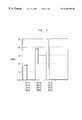
- a typical semiconductor deviceincludes a substrate 12 , an isolation structure in the substrate (e.g., shallow trench isolation 10 ), an active device structure (e.g., a transistor structure 14 , 16 , 18 , 19 , 20 ), a dielectric layer 26 over the active device structure, and a metal interconnect layer 28 over the dielectric layer (metal-1 level).
- At least one of the isolation structure 10 and the dielectric layer 26which are dielectric material components in the front-end structure—comprise a material exhibiting a dielectric constant less than 3.5. This relatively low dielectric constant provides improved properties in the overall device by reducing capacitive coupling in the front-end.
- low ⁇ materials designed for a back-end structuremust meet a different set of physical and chemical requirements.
- the thermal stability requirement for front-end low ⁇ materialsis much higher, typically at least 700° C., and as high as 1000° C.
- typical back-end low ⁇ materialssuch as organic or inorganic polymers generally are designed to endure only relatively low temperatures, e.g., up to 425° C., and will not withstand front-end processing temperatures.
- a high thermal stability porous silicais used to provide a dielectric constant less than 3.5, advantageously less than 3.0, in the front-end structure of semiconductor devices.
- the silicais capable of exhibiting a thermal stability of at least 700° C., optionally at least 1000° C. (Thermal stability indicates less than 5 wt.% loss at the noted temperature.)
- FIG. 1illustrates a typical MOSFET device structure.
- FIG. 2illustrates the capacitive coupling exhibited by a MOSFET structure such as illustrated in FIG. 1 .
- FIG. 3illustrates the device structure used for a simulation experiment involving variation in dielectric constant values.
- FIG. 4illustrates the effect of providing low ⁇ material in the front-end structure.
- the inventionprovides a device comprising a substrate (generally silicon, gallium arsenide, or silicon-on-insulator), an isolation structure in the substrate (e.g., shallow trench isolation), an active device structure (e.g., a transistor structure), a dielectric layer over the active device structure, and a metal interconnect layer over the dielectric layer (metal-1 level).
- a substrategenerally silicon, gallium arsenide, or silicon-on-insulator
- an isolation structure in the substratee.g., shallow trench isolation
- an active device structuree.g., a transistor structure
- a dielectric layerover the active device structure
- metal interconnect layerover the dielectric layer
- FIG. 1The basic architecture of a common silicon semiconductor device—a metal-oxide-silicon field effect transistor (MOSFET)—is presented in FIG. 1 .
- MOSFETmetal-oxide-silicon field effect transistor
- This isolation structure 10is typically formed by patterning trenches into a silicon substrate 12 and filling the trenches with an insulating material such as silicon dioxide (known as shallow trench isolation). Additional processes remove the insulating material from the areas of the silicon 12 surface where MOSFET devices are to be formed.
- shallow trench isolationis capable of providing such isolation, with shallow trench isolation being the most common for deep sub-micron ( ⁇ 0.35 ⁇ m) devices.
- the active device structure(i.e., the components in which the desired electrical activity occurs)—in this case a transistor—contains a gate conductor 14 typically formed from polysilicon, a gate dielectric 16 , and a gate junction 18 .
- the junction 18is generally formed by doping the silicon with either n-type (e.g. phosphorus) or p-type (e.g. boron) impurities and activating them with high temperature (>900° C.) anneal.
- the junctiongenerally consists of two regions: a lightly doped region 19 next to the transistor channel and under the gate dielectric, and a more heavily doped region 20 .
- the most common way to produce two regionsis to use an insulating spacer 22 .
- a light-dose (e.g., 10 13 -10 14 cm ⁇ 2 ) ion implantationis performed after the gate definition.
- the spacer 22is formed by depositing and then etching an insulating material. Heavier-dose (>10 15 cm ⁇ 2 ) ion implantation is then performed, with the spacer 22 protecting the lightly doped region from this second implantation.
- a layer of insulating material 26is deposited over the active device, this layer 26 generally referred to as dielectric-1 (D-1).
- D-1dielectric-1
- contact holesare patterned into the dielectric-1 layer 26 , and metal wiring 24 is provided in the contact holes, the wiring 24 in contact with a metal interconnect layer 28 .
- multiple levels of metal interconnecte.g., 5-7 levels, are used, with insulating material between each level.
- the structure from the substrate 12 up to the first metal interconnect level 28is referred to as the front-end structure.
- FIG. 2illustrates different types of capacitive coupling that exist in the front-end structure of a MOSFET device as shown in FIG. 1 .
- These couplingsinclude: (A) first metal wiring (Metal-1) to silicon substrate, (B) Metal-1 to junctions, (C) Metal-1 to gate, (D) gate to silicon substrate, and (E) gate to adjacent junctions.
- Using low ⁇ material in the dielectric layer 26 , the isolation structure 10 , and the spacer 22is effective in reducing these couplings.
- the couplingis affected by dielectric layer 26 (D-1) and the isolation structure 10 .
- D-1For couplings (B) and (C), only D-1 has an effect.
- the isolation structure 10For capacitive coupling (D), only the isolation structure 10 has an effect. In the case of coupling (E), the spacer 22 plays an important role.
- the gate insulator 16is required to provide a strong capacitive coupling between the gate and the transistor channel for effective ULSI device operation. Therefore, low ⁇ material is generally not suitable for the gate insulator.
- the capacitance of these couplingsis capable of being reduced by providing materials with relatively low dielectric constant ( ⁇ 3.5) in the front-end structure, e.g., for the spacer 22 , the dielectric-1 level 26 , and the isolation structure 10 . And, by reducing the capacitance, the overall device exhibits improved properties. In fact, using low ⁇ material in the front-end structure is more effective in improving performance than using such low ⁇ material in the back-end structure.
- the low dielectric constant materialmust exhibit high thermal stability.
- Porous inorganic materialshave been found to be useful because the ⁇ value derives from a combination of that of air ( ⁇ 1) and of a high thermal stability solid phase.
- the low ⁇ materialis thermally stable (weight loss ⁇ 5%) at the requisite temperature, typically 700 to 1000° C., depending on the particular area of incorporation.
- the dielectric layer (D-1)typically experiences temperatures of up to 700° C., the spacer up to 800° C., and the isolation structure up to 1000° C.
- the porosity and the surrounding structureadvantageously remain nearly constant during the processing, without substantial pore collapse or pore growth.
- Suitable materialsinclude ceramics such as silica and alumina. Other materials such as porous diamond-like-carbon (DLC) and some thermosetting polymers are also contemplated.
- the average pore sizeis generally much smaller than microelectronics feature sizes.
- the porosityis typically in the range 10 to 90 vol. %, advantageously 10-60 vol. %, in order to provide a low ⁇ value, while at the same time provide sufficient mechanical strength.
- the dielectric constantis advantageously below 3.5, more advantageously below 3.0.
- the pore sizeis advantageously less than 25 nm, more advantageously less than 15 nm.
- a narrow pore size distributionis desired, advantageously such that the tail of large pore sizes terminates below 25 nm.
- Porous silicais useful for several reasons. Specifically, silica is a commonly-used dielectric material and porous silica fabrication techniques employ precursors similar to those used for conventional silica deposition, e.g., spin on glass (SOG) and chemical vapor deposition (CVD). Porous silica is generally classified as either an aerogel (dried supercritically, containing >75% voids) or a xerogel (dried by solvent evaporation, containing ⁇ 75% voids). Both types of porous silica are referred to herein as nanoporous silica (NPS). In addition to exhibiting a low ⁇ , NPS is capable of being formed such that it exhibits a thermal stability up to 1000° C. NPS also offers small pore sizes (less than the size of microelectronics features), is capable of deposition using similar tools as employed for conventional SOG processing, and offers the ability to tune dielectric constant over a wide range by varying porosity.
- SOGspin on glass
- the NPSlow ⁇ material by any suitable technique.
- the NPSis fabricated by solution sol gel or colloidal sol gel techniques, using, for example, spin-on coating processes.
- the solution sol gel techniquetypically involves the use of precursors such as alkoxysilanes, in particular tetraethoxysilane (TEOS), and alkylalkoxysilanes, in particular methyltriethoxysilane (MTEOS).
- TEOStetraethoxysilane
- MTEOSmethyltriethoxysilane
- the porosityis created by allowing the precursor films to gel (i.e. cross-link to yield a continuous solid network spanning the entire fluid) before drying, such that removal of the water leaves air-filled pores. Gelation occurs after precursor deposition either as a result of changes in the precursor immediately before deposition (temperature, pH, catalyst, etc.), as a result of a catalyst added after deposition, or by evaporation after deposition. Chemical and processing considerations include precursor chemistry, control of solvent evaporation, aging to maximize film strength, and preventing shrinkage during drying.
- colloidal sol gel processesare possible.
- One processinvolves the use of colloidal silica and potassium silicate. See, e.g., E. D. Birdsell and R. A. Gerhardt, “Porous silica: a potential material for low dielectric constant applications,” MRS Symp. Proceedings on Low Dielectric Constant Materials , Vol. 511, 111 (1998).
- the precursorsare combined with a gelling agent such as formamide, and mixed at room temperature.
- a gelling agentsuch as formamide
- the filmsare typically gelled in normal atmospheric conditions, leached with deionized water to remove the remnant alkali ions, air dried and then baked.
- Important process parametersinclude the spin speed, precursor mixing time, gelation time, and gel composition (ratio of colloidal silica to potassium silicate).
- Aerogelsare typically made by such sol gel techniques, but involve formation of solvent-filled gels which are dried using special conditions to preserve the solid network. Preparation of high porosity aerogel films is known in the art, as reflected, for example, in L. W. Hrubesh and J. F. Poco, “Processing and characterization of high porosity aerogel films,” MRS Symp. Proceedings on Advances in Porous Materials , Vol. 371, 195 (1995). Aerogels often have extremely high porosity, however, which creates the potential for reduced strength.
- Sol gel processesare easily adapted to deposit porous material such as NPS (xerogel and/or aerogel) into the front-end structure of a semiconductor device.
- a typical front-end fabrication processinvolves approximately 250 steps, as known in the art.
- Optional steps involving deposition of low ⁇ front-end materialsinclude the following.
- the shallow isolation trenchis capable of being filled by spinning-on silica sol.
- the trench materialis typically polished via CMP (chemical-mechanical polishing) to the level of the substrate surface.
- CMPchemical-mechanical polishing
- the spacer dielectricis formed by spinning-on silica sol and gelling the material, followed by anisotropic etch.
- dielectric-1is deposited by spinning-on silica sol, followed by gelling and CMP to planarize the dielectric-1. Steps of forming windows in dielectric-1 as well as metal-1 formation follow.
- a circuit simulation using different dielectric structureswas performed using a TCAD simulator, ADVICE TM .
- the circuita divide-by-three counter, was a standard ASIC bench-mark test circuit, and the maximum toggling frequency of the counter just prior to a functional failure was recorded.
- the design rule used for the circuitwas based on a 0.25 ⁇ m CMOS design rule, and both the layout design rule and the circuit (poly-cell) weighted rule for poly-1 (gate conductor), metal-1 and metal-2 are listed in Table I.
- the weighted circuit rulewas used in the simulation for capacitance extraction.
- the capacitance extractionwas done using the device structure shown in FIG. 3 .
- the structurecontains a substrate (SB), a gate junction (DF), gate conductors (PL), dielectric levels 1 , 2 , and 3 (D 1 , D 2 , D 3 , respectively), and metal interconnect levels 1 and 2 (M 1 and M 2 , respectively).
- the thicknesses in the deviceswere as follows:
- D 44 and D 22are two dielectric systems in which the dielectric materials have a dielectric constant of 4.0 and 2.0, respectively, from D 1 and up.
- D 42is a dielectric system using dielectric material with a dielectric constant of 2 from D 2 and up.
- Table IIThe extracted capacitance values from the circuit simulation are listed in Table II and illustrated in FIG. 4 .
- Table IIprovides a breakdown of the capacitance contributions due to addition of low ⁇ material into the circuit simulation one capacitive parameter at a time. Both inter-capacitance (between metal layers—in capacitance per area) and intra-capacitance (between metal lines—in capacitance per length) are listed.
- the simulationbegan from a circuit with dielectric system of D 44 , migrated into circuit with dielectric system of D 42 , and concluded at a circuit with dielectric system of D 22 . For each simulation, the maximum toggling frequency (f max ) for the divide-by-three counter was obtained and used as a measure of the circuit performance.
- capacitance Ametal-1 to substrate—CM 1 SB
- Bmetal- 1 to junction or CM 1 DF
- Cmetal-1 to gate conductor or M 1 PL
- parasitic capacitance Dgate conductor to substrate or CPLSB
Landscapes
- Physics & Mathematics (AREA)
- Condensed Matter Physics & Semiconductors (AREA)
- General Physics & Mathematics (AREA)
- Engineering & Computer Science (AREA)
- Computer Hardware Design (AREA)
- Microelectronics & Electronic Packaging (AREA)
- Power Engineering (AREA)
- Internal Circuitry In Semiconductor Integrated Circuit Devices (AREA)
- Insulated Gate Type Field-Effect Transistor (AREA)
- Element Separation (AREA)
- Semiconductor Integrated Circuits (AREA)
- Formation Of Insulating Films (AREA)
Abstract
Description
| TABLE I |
| 0.25 μm design rule and circuit averaged rule for a poly-cell divide- |
| by-three counter layout and circuit simulation |
| Design Rule | Poly-Cell Averaged | |||
| Level | <line>/<space> | <line>/<space> | ||
| P1 | 0.25 μm/0.36 μm | 0.25 μm/0.50 μm | ||
| M1 | 0.40 μm/0.40 μm | 0.40 μm/0.50 μm | ||
| M2 | 0.40 μm/0.40 μm | 0.40 μm/0.60 μm | ||
| TABLE II | ||||||||||
| CPLSB | CM1SB | CM1DF | CM1PL | CM2SB | CM2DF | CM2PL | CM2M1 | (fmax) | ||
| D = 44 | |||||||||
| Inter | 29.36 | 5.93 | 7.59 | 9.38 | 3.35 | 3.78 | 4.10 | 10.23 | 1.34 |
| Intra | 2.99 | 6.73 | 6.53 | 6.33 | 8.01 | 7.95 | 7.90 | 7.18 | |
| — | — | — | — | — | — | — | 5.10 | 1.34 | |
| — | — | — | — | — | — | — | 3.59 | ||
| — | — | — | — | — | — | 2.05 | 5.10 | 1.34 | |
| — | — | — | — | — | — | 3.95 | 3.59 | ||
| — | — | — | — | — | 1.88 | 2.05 | 5.10 | 1.34 | |
| — | — | — | — | — | 3.97 | 3.95 | 3.59 | ||
| — | — | — | — | 1.68 | 1.88 | 2.05 | 5.10 | 1.35 | |
| — | — | — | — | 4.00 | 3.97 | 3.95 | 3.59 | ||
| — | — | — | 9.13 | 1.68 | 1.88 | 2.05 | 5.10 | 1.37 | |
| — | — | — | 3.57 | 4.00 | 3.97 | 3.95 | 3.59 | ||
| — | — | 7.43 | 9.13 | 1.68 | 1.88 | 2.05 | 5.10 | 1.39 | |
| — | — | 3.76 | 3.57 | 4.00 | 3.97 | 3.95 | 3.59 | ||
| D = 42 | |||||||||
| Inter | 29.36 | 5.80 | 7.43 | 9.13 | 1.68 | 1.88 | 2.05 | 5.10 | 1.44 |
| Intra | 2.99 | 3.96 | 3.76 | 3.57 | 4.00 | 3.97 | 3.95 | 3.59 | |
| — | — | — | 4.67 | 1.68 | 1.88 | 2.05 | 5.10 | 1.45 | |
| — | — | — | 3.16 | 4.00 | 3.97 | 3.95 | 3.59 | ||
| — | — | 3.80 | 4.67 | 1.68 | 1.88 | 2.05 | 5.10 | 1.46 | |
| — | — | 3.26 | 3.16 | 4.00 | 3.97 | 3.95 | 3.59 | ||
| — | 2.95 | 3.80 | 4.67 | 1.68 | 1.88 | 2.05 | 5.10 | 1.48 | |
| — | 3.37 | 3.26 | 3.16 | 4.00 | 3.97 | 3.95 | 3.59 | ||
| D = 22 | |||||||||
| Inter | 27.32 | 2.95 | 3.80 | 4.67 | 1.68 | 1.88 | 2.05 | 5.10 | 1.5 |
| Intra | 1.50 | 3.37 | 3.26 | 3.16 | 4.00 | 3.97 | 3.95 | 3.59 | |
| Capacitance units: Inter (between levels) = E-17 (f/μm2), Intra (between lines) = E-17 (f/μm) | |||||||||
Claims (19)
Priority Applications (5)
| Application Number | Priority Date | Filing Date | Title |
|---|---|---|---|
| US09/296,001US6469390B2 (en) | 1999-01-26 | 1999-04-21 | Device comprising thermally stable, low dielectric constant material |
| TW088119586ATW441064B (en) | 1999-01-26 | 1999-11-09 | Device comprising thermally stable, low dielectric constant meterial |
| EP00300387AEP1024534A3 (en) | 1999-01-26 | 2000-01-19 | Device comprising thermally stable, low dielectric constant material |
| JP2000015643AJP2000223572A (en) | 1999-01-26 | 2000-01-25 | Device with thermally stable and low dielectric constant material |
| KR1020000003582AKR20000057806A (en) | 1999-01-26 | 2000-01-26 | Device comprising thermally stable, low dielectric constant material |
Applications Claiming Priority (2)
| Application Number | Priority Date | Filing Date | Title |
|---|---|---|---|
| US11724299P | 1999-01-26 | 1999-01-26 | |
| US09/296,001US6469390B2 (en) | 1999-01-26 | 1999-04-21 | Device comprising thermally stable, low dielectric constant material |
Publications (2)
| Publication Number | Publication Date |
|---|---|
| US20020000669A1 US20020000669A1 (en) | 2002-01-03 |
| US6469390B2true US6469390B2 (en) | 2002-10-22 |
Family
ID=26815083
Family Applications (1)
| Application Number | Title | Priority Date | Filing Date |
|---|---|---|---|
| US09/296,001Expired - LifetimeUS6469390B2 (en) | 1999-01-26 | 1999-04-21 | Device comprising thermally stable, low dielectric constant material |
Country Status (5)
| Country | Link |
|---|---|
| US (1) | US6469390B2 (en) |
| EP (1) | EP1024534A3 (en) |
| JP (1) | JP2000223572A (en) |
| KR (1) | KR20000057806A (en) |
| TW (1) | TW441064B (en) |
Cited By (7)
| Publication number | Priority date | Publication date | Assignee | Title |
|---|---|---|---|---|
| US20030057414A1 (en)* | 2000-12-18 | 2003-03-27 | International Business Machines Corporation | Method for forming a porous dielectric material layer in a semiconductor device and device formed |
| US20030128944A1 (en)* | 2002-01-09 | 2003-07-10 | Ceramoptec Industries, Inc. | Device and method to scatter optical fiber output |
| US6653718B2 (en)* | 2001-01-11 | 2003-11-25 | Honeywell International, Inc. | Dielectric films for narrow gap-fill applications |
| US6812527B2 (en)* | 2002-09-05 | 2004-11-02 | International Business Machines Corporation | Method to control device threshold of SOI MOSFET's |
| US7032457B1 (en)* | 2002-09-27 | 2006-04-25 | Nanodynamics, Inc. | Method and apparatus for dielectric sensors and smart skin for aircraft and space vehicles |
| US20080061403A1 (en)* | 2006-09-08 | 2008-03-13 | Zhong-Xiang He | Dielectric layers for metal lines in semiconductor chips |
| US20080093679A1 (en)* | 2005-01-18 | 2008-04-24 | Tohoku University | Semiconductor Device |
Families Citing this family (5)
| Publication number | Priority date | Publication date | Assignee | Title |
|---|---|---|---|---|
| US6495479B1 (en)* | 2000-05-05 | 2002-12-17 | Honeywell International, Inc. | Simplified method to produce nanoporous silicon-based films |
| US7081393B2 (en)* | 2004-05-20 | 2006-07-25 | International Business Machines Corporation | Reduced dielectric constant spacer materials integration for high speed logic gates |
| JP2005340327A (en) | 2004-05-25 | 2005-12-08 | Renesas Technology Corp | Semiconductor device and manufacturing method thereof |
| US20090026924A1 (en)* | 2007-07-23 | 2009-01-29 | Leung Roger Y | Methods of making low-refractive index and/or low-k organosilicate coatings |
| CN112071915B (en)* | 2019-06-10 | 2025-07-22 | 堺显示器制品株式会社 | Thin film transistor, method of manufacturing the same, and display device |
Citations (8)
| Publication number | Priority date | Publication date | Assignee | Title |
|---|---|---|---|---|
| US4222792A (en) | 1979-09-10 | 1980-09-16 | International Business Machines Corporation | Planar deep oxide isolation process utilizing resin glass and E-beam exposure |
| US5217920A (en) | 1992-06-18 | 1993-06-08 | Motorola, Inc. | Method of forming substrate contact trenches and isolation trenches using anodization for isolation |
| US5470802A (en) | 1994-05-20 | 1995-11-28 | Texas Instruments Incorporated | Method of making a semiconductor device using a low dielectric constant material |
| US5548159A (en) | 1994-05-27 | 1996-08-20 | Texas Instruments Incorporated | Porous insulator for line-to-line capacitance reduction |
| US5668398A (en) | 1994-05-27 | 1997-09-16 | Texas Instruments Incorporated | Multilevel interconnect structure with air gaps formed between metal leads |
| US5751056A (en) | 1994-05-31 | 1998-05-12 | Texas Instruments Incorporated | Reliable metal leads in high speed LSI semiconductors using dummy leads |
| US5751066A (en) | 1994-05-27 | 1998-05-12 | Texas Instruments Incorporated | Structure with selective gap fill of submicron interconnects |
| US5750415A (en) | 1994-05-27 | 1998-05-12 | Texas Instruments Incorporated | Low dielectric constant layers via immiscible sol-gel processing |
Family Cites Families (6)
| Publication number | Priority date | Publication date | Assignee | Title |
|---|---|---|---|---|
| US4994404A (en)* | 1989-08-28 | 1991-02-19 | Motorola, Inc. | Method for forming a lightly-doped drain (LDD) structure in a semiconductor device |
| JP2560637B2 (en)* | 1994-04-28 | 1996-12-04 | 日本電気株式会社 | Field effect transistor and method of manufacturing the same |
| JP3413823B2 (en)* | 1996-03-07 | 2003-06-09 | 日本電気株式会社 | Semiconductor device and manufacturing method thereof |
| JPH09260369A (en)* | 1996-03-25 | 1997-10-03 | Toshiba Corp | Method of forming insulating film |
| AU7371898A (en)* | 1997-05-07 | 1998-11-27 | Mark J. Hampden-Smith | Low density film for low dielectric constant applications |
| KR19980087552A (en)* | 1997-05-28 | 1998-12-05 | 윌리엄 버. 켐플러 | Integrated circuit dielectric and method |
- 1999
- 1999-04-21USUS09/296,001patent/US6469390B2/ennot_activeExpired - Lifetime
- 1999-11-09TWTW088119586Apatent/TW441064B/ennot_activeIP Right Cessation
- 2000
- 2000-01-19EPEP00300387Apatent/EP1024534A3/ennot_activeWithdrawn
- 2000-01-25JPJP2000015643Apatent/JP2000223572A/enactivePending
- 2000-01-26KRKR1020000003582Apatent/KR20000057806A/ennot_activeAbandoned
Patent Citations (8)
| Publication number | Priority date | Publication date | Assignee | Title |
|---|---|---|---|---|
| US4222792A (en) | 1979-09-10 | 1980-09-16 | International Business Machines Corporation | Planar deep oxide isolation process utilizing resin glass and E-beam exposure |
| US5217920A (en) | 1992-06-18 | 1993-06-08 | Motorola, Inc. | Method of forming substrate contact trenches and isolation trenches using anodization for isolation |
| US5470802A (en) | 1994-05-20 | 1995-11-28 | Texas Instruments Incorporated | Method of making a semiconductor device using a low dielectric constant material |
| US5548159A (en) | 1994-05-27 | 1996-08-20 | Texas Instruments Incorporated | Porous insulator for line-to-line capacitance reduction |
| US5668398A (en) | 1994-05-27 | 1997-09-16 | Texas Instruments Incorporated | Multilevel interconnect structure with air gaps formed between metal leads |
| US5751066A (en) | 1994-05-27 | 1998-05-12 | Texas Instruments Incorporated | Structure with selective gap fill of submicron interconnects |
| US5750415A (en) | 1994-05-27 | 1998-05-12 | Texas Instruments Incorporated | Low dielectric constant layers via immiscible sol-gel processing |
| US5751056A (en) | 1994-05-31 | 1998-05-12 | Texas Instruments Incorporated | Reliable metal leads in high speed LSI semiconductors using dummy leads |
Non-Patent Citations (7)
| Title |
|---|
| E. D. Birdsell, et al., "Porous silica: a potential material for low dielectric constant applications," MRS Symp. Proceedings on Low Dielectric Constant Materials, vol. 511, 111 (1998). |
| L. Peters, "Pursuing the perfect low-k dielectric", Semiconductor International, 64 (1998). |
| L.W. Hurbesh, et al., "Processing and characterization of high porosity aerogel films," MRS. Symp. Proceedings on Advances in Porous Materials, vol. 371, 195 (1995). |
| MRS Bulletin on Low Dielectric Constant Materials, vol. 22, (1997). |
| MRS Symposium Proceedings on Low Dielectric Constant Materials, vols. 381, 443, 476, 511, (1995-1998). |
| P. Singer, "Low k dielectircs: the search continues," Semiconductor International, 64 (1998). |
| T. Ramos et al., "Nanoporous silica for low k dielectrics," MRS. Symp. Proceedings on Low Dielectric Constant Materials, vol. 443, 91 (1997). |
Cited By (12)
| Publication number | Priority date | Publication date | Assignee | Title |
|---|---|---|---|---|
| US20030057414A1 (en)* | 2000-12-18 | 2003-03-27 | International Business Machines Corporation | Method for forming a porous dielectric material layer in a semiconductor device and device formed |
| US6831364B2 (en)* | 2000-12-18 | 2004-12-14 | International Business Machines Corporation | Method for forming a porous dielectric material layer in a semiconductor device and device formed |
| US6653718B2 (en)* | 2001-01-11 | 2003-11-25 | Honeywell International, Inc. | Dielectric films for narrow gap-fill applications |
| US20030128944A1 (en)* | 2002-01-09 | 2003-07-10 | Ceramoptec Industries, Inc. | Device and method to scatter optical fiber output |
| US6810184B2 (en)* | 2002-01-09 | 2004-10-26 | Ceram Optec Industries Inc. | Device and method to scatter optical fiber output |
| US6812527B2 (en)* | 2002-09-05 | 2004-11-02 | International Business Machines Corporation | Method to control device threshold of SOI MOSFET's |
| US20050048703A1 (en)* | 2002-09-05 | 2005-03-03 | International Business Machines Corporation | Method to control device threshold of SOI MOSFET's |
| US7273785B2 (en) | 2002-09-05 | 2007-09-25 | International Business Machines Corporation | Method to control device threshold of SOI MOSFET's |
| US7032457B1 (en)* | 2002-09-27 | 2006-04-25 | Nanodynamics, Inc. | Method and apparatus for dielectric sensors and smart skin for aircraft and space vehicles |
| US20080093679A1 (en)* | 2005-01-18 | 2008-04-24 | Tohoku University | Semiconductor Device |
| US7893537B2 (en) | 2005-01-18 | 2011-02-22 | Tohoku Uinversity | Semiconductor device |
| US20080061403A1 (en)* | 2006-09-08 | 2008-03-13 | Zhong-Xiang He | Dielectric layers for metal lines in semiconductor chips |
Also Published As
| Publication number | Publication date |
|---|---|
| US20020000669A1 (en) | 2002-01-03 |
| KR20000057806A (en) | 2000-09-25 |
| EP1024534A3 (en) | 2003-08-06 |
| EP1024534A2 (en) | 2000-08-02 |
| TW441064B (en) | 2001-06-16 |
| JP2000223572A (en) | 2000-08-11 |
Similar Documents
| Publication | Publication Date | Title |
|---|---|---|
| US6469390B2 (en) | Device comprising thermally stable, low dielectric constant material | |
| KR100416681B1 (en) | Porous silicon oxycarbide integrated circuit insulator | |
| US6737723B2 (en) | Low dielectric constant shallow trench isolation | |
| US7888722B2 (en) | Trench capacitors and memory cells using trench capacitors | |
| US5313094A (en) | Thermal dissipation of integrated circuits using diamond paths | |
| US6498062B2 (en) | DRAM access transistor | |
| KR100561990B1 (en) | Semiconductor devices | |
| US20160276260A1 (en) | Metal interconnect structure and method for fabricating the same | |
| KR101795867B1 (en) | Buried channel semiconductor device and method for manufacturing the same | |
| US7235493B2 (en) | Low-k dielectric process for multilevel interconnection using mircocavity engineering during electric circuit manufacture | |
| KR20040038820A (en) | Semiconductor device with dummy structure | |
| US6649503B2 (en) | Methods of fabricating integrated circuit devices having spin on glass (SOG) insulating layers and integrated circuit devices fabricated thereby | |
| US6770570B2 (en) | Method of forming a semiconductor device with a substantially uniform density low-k dielectric layer | |
| KR100774600B1 (en) | Semiconductor devices with reduced line-to-line capacitance and crosstalk noise | |
| US20140179071A1 (en) | Two-step shallow trench isolation (sti) process | |
| US10438893B2 (en) | Metal interconnect structure and method for fabricating the same | |
| US6472700B2 (en) | Semiconductor device with isolation insulator, interlayer insulation film, and a sidewall coating film | |
| KR20210138927A (en) | Method for fabricating semiconductor device | |
| US6124191A (en) | Self-aligned contact process using low density/low k dielectric | |
| KR100756788B1 (en) | Manufacturing method of semiconductor device | |
| US6395611B1 (en) | Inductor or low loss interconnect and a method of manufacturing an inductor or low loss interconnect in an integrated circuit | |
| US20080142861A1 (en) | Symmetric capacitor structure | |
| US20250246542A1 (en) | Semiconductor device with liner structure and method for fabricating the same | |
| US20250194210A1 (en) | Semiconductor structure with extended backside connections | |
| KR100280808B1 (en) | Manufacturing Method of Semiconductor Device |
Legal Events
| Date | Code | Title | Description |
|---|---|---|---|
| AS | Assignment | Owner name:LUCENT TECHNOLOGIES INC., NEW JERSEY Free format text:ASSIGNMENT OF ASSIGNORS INTEREST;ASSIGNORS:CHANG, CHORNG-PING;CHEUNG, KIN PING;PAI, CHLEN-SHING;AND OTHERS;REEL/FRAME:009909/0063;SIGNING DATES FROM 19990415 TO 19990420 | |
| STCF | Information on status: patent grant | Free format text:PATENTED CASE | |
| FEPP | Fee payment procedure | Free format text:PAYOR NUMBER ASSIGNED (ORIGINAL EVENT CODE: ASPN); ENTITY STATUS OF PATENT OWNER: LARGE ENTITY | |
| FPAY | Fee payment | Year of fee payment:4 | |
| FPAY | Fee payment | Year of fee payment:8 | |
| FPAY | Fee payment | Year of fee payment:12 | |
| AS | Assignment | Owner name:DEUTSCHE BANK AG NEW YORK BRANCH, AS COLLATERAL AG Free format text:PATENT SECURITY AGREEMENT;ASSIGNORS:LSI CORPORATION;AGERE SYSTEMS LLC;REEL/FRAME:032856/0031 Effective date:20140506 | |
| AS | Assignment | Owner name:AVAGO TECHNOLOGIES GENERAL IP (SINGAPORE) PTE. LTD Free format text:ASSIGNMENT OF ASSIGNORS INTEREST;ASSIGNOR:AGERE SYSTEMS LLC;REEL/FRAME:035365/0634 Effective date:20140804 | |
| AS | Assignment | Owner name:AGERE SYSTEMS LLC, PENNSYLVANIA Free format text:TERMINATION AND RELEASE OF SECURITY INTEREST IN PATENT RIGHTS (RELEASES RF 032856-0031);ASSIGNOR:DEUTSCHE BANK AG NEW YORK BRANCH, AS COLLATERAL AGENT;REEL/FRAME:037684/0039 Effective date:20160201 Owner name:LSI CORPORATION, CALIFORNIA Free format text:TERMINATION AND RELEASE OF SECURITY INTEREST IN PATENT RIGHTS (RELEASES RF 032856-0031);ASSIGNOR:DEUTSCHE BANK AG NEW YORK BRANCH, AS COLLATERAL AGENT;REEL/FRAME:037684/0039 Effective date:20160201 | |
| AS | Assignment | Owner name:BANK OF AMERICA, N.A., AS COLLATERAL AGENT, NORTH CAROLINA Free format text:PATENT SECURITY AGREEMENT;ASSIGNOR:AVAGO TECHNOLOGIES GENERAL IP (SINGAPORE) PTE. LTD.;REEL/FRAME:037808/0001 Effective date:20160201 Owner name:BANK OF AMERICA, N.A., AS COLLATERAL AGENT, NORTH Free format text:PATENT SECURITY AGREEMENT;ASSIGNOR:AVAGO TECHNOLOGIES GENERAL IP (SINGAPORE) PTE. LTD.;REEL/FRAME:037808/0001 Effective date:20160201 | |
| AS | Assignment | Owner name:AVAGO TECHNOLOGIES GENERAL IP (SINGAPORE) PTE. LTD., SINGAPORE Free format text:TERMINATION AND RELEASE OF SECURITY INTEREST IN PATENTS;ASSIGNOR:BANK OF AMERICA, N.A., AS COLLATERAL AGENT;REEL/FRAME:041710/0001 Effective date:20170119 Owner name:AVAGO TECHNOLOGIES GENERAL IP (SINGAPORE) PTE. LTD Free format text:TERMINATION AND RELEASE OF SECURITY INTEREST IN PATENTS;ASSIGNOR:BANK OF AMERICA, N.A., AS COLLATERAL AGENT;REEL/FRAME:041710/0001 Effective date:20170119 | |
| AS | Assignment | Owner name:BELL SEMICONDUCTOR, LLC, ILLINOIS Free format text:ASSIGNMENT OF ASSIGNORS INTEREST;ASSIGNORS:AVAGO TECHNOLOGIES GENERAL IP (SINGAPORE) PTE. LTD.;BROADCOM CORPORATION;REEL/FRAME:044886/0001 Effective date:20171208 | |
| AS | Assignment | Owner name:CORTLAND CAPITAL MARKET SERVICES LLC, AS COLLATERA Free format text:SECURITY INTEREST;ASSIGNORS:HILCO PATENT ACQUISITION 56, LLC;BELL SEMICONDUCTOR, LLC;BELL NORTHERN RESEARCH, LLC;REEL/FRAME:045216/0020 Effective date:20180124 | |
| AS | Assignment | Owner name:BELL NORTHERN RESEARCH, LLC, ILLINOIS Free format text:SECURITY INTEREST;ASSIGNOR:CORTLAND CAPITAL MARKET SERVICES LLC;REEL/FRAME:060885/0001 Effective date:20220401 Owner name:BELL SEMICONDUCTOR, LLC, ILLINOIS Free format text:SECURITY INTEREST;ASSIGNOR:CORTLAND CAPITAL MARKET SERVICES LLC;REEL/FRAME:060885/0001 Effective date:20220401 Owner name:HILCO PATENT ACQUISITION 56, LLC, ILLINOIS Free format text:SECURITY INTEREST;ASSIGNOR:CORTLAND CAPITAL MARKET SERVICES LLC;REEL/FRAME:060885/0001 Effective date:20220401 |