US6468413B1 - Electrochemical etch for high tin solder bumps - Google Patents
Electrochemical etch for high tin solder bumpsDownload PDFInfo
- Publication number
- US6468413B1 US6468413B1US09/697,333US69733300AUS6468413B1US 6468413 B1US6468413 B1US 6468413B1US 69733300 AUS69733300 AUS 69733300AUS 6468413 B1US6468413 B1US 6468413B1
- Authority
- US
- United States
- Prior art keywords
- lead
- tin
- metals
- range
- concentration
- Prior art date
- Legal status (The legal status is an assumption and is not a legal conclusion. Google has not performed a legal analysis and makes no representation as to the accuracy of the status listed.)
- Expired - Lifetime, expires
Links
Images


Classifications
- C—CHEMISTRY; METALLURGY
- C25—ELECTROLYTIC OR ELECTROPHORETIC PROCESSES; APPARATUS THEREFOR
- C25F—PROCESSES FOR THE ELECTROLYTIC REMOVAL OF MATERIALS FROM OBJECTS; APPARATUS THEREFOR
- C25F3/00—Electrolytic etching or polishing
- C25F3/02—Etching
- H—ELECTRICITY
- H01—ELECTRIC ELEMENTS
- H01L—SEMICONDUCTOR DEVICES NOT COVERED BY CLASS H10
- H01L21/00—Processes or apparatus adapted for the manufacture or treatment of semiconductor or solid state devices or of parts thereof
- H01L21/02—Manufacture or treatment of semiconductor devices or of parts thereof
- H01L21/04—Manufacture or treatment of semiconductor devices or of parts thereof the devices having potential barriers, e.g. a PN junction, depletion layer or carrier concentration layer
- H01L21/18—Manufacture or treatment of semiconductor devices or of parts thereof the devices having potential barriers, e.g. a PN junction, depletion layer or carrier concentration layer the devices having semiconductor bodies comprising elements of Group IV of the Periodic Table or AIIIBV compounds with or without impurities, e.g. doping materials
- H01L21/30—Treatment of semiconductor bodies using processes or apparatus not provided for in groups H01L21/20 - H01L21/26
- H01L21/31—Treatment of semiconductor bodies using processes or apparatus not provided for in groups H01L21/20 - H01L21/26 to form insulating layers thereon, e.g. for masking or by using photolithographic techniques; After treatment of these layers; Selection of materials for these layers
- H01L21/3205—Deposition of non-insulating-, e.g. conductive- or resistive-, layers on insulating layers; After-treatment of these layers
- H01L21/321—After treatment
- H01L21/3213—Physical or chemical etching of the layers, e.g. to produce a patterned layer from a pre-deposited extensive layer
- H01L21/32133—Physical or chemical etching of the layers, e.g. to produce a patterned layer from a pre-deposited extensive layer by chemical means only
- H01L21/32134—Physical or chemical etching of the layers, e.g. to produce a patterned layer from a pre-deposited extensive layer by chemical means only by liquid etching only
- H—ELECTRICITY
- H01—ELECTRIC ELEMENTS
- H01L—SEMICONDUCTOR DEVICES NOT COVERED BY CLASS H10
- H01L24/00—Arrangements for connecting or disconnecting semiconductor or solid-state bodies; Methods or apparatus related thereto
- H01L24/01—Means for bonding being attached to, or being formed on, the surface to be connected, e.g. chip-to-package, die-attach, "first-level" interconnects; Manufacturing methods related thereto
- H01L24/02—Bonding areas ; Manufacturing methods related thereto
- H01L24/03—Manufacturing methods
- H—ELECTRICITY
- H01—ELECTRIC ELEMENTS
- H01L—SEMICONDUCTOR DEVICES NOT COVERED BY CLASS H10
- H01L24/00—Arrangements for connecting or disconnecting semiconductor or solid-state bodies; Methods or apparatus related thereto
- H01L24/01—Means for bonding being attached to, or being formed on, the surface to be connected, e.g. chip-to-package, die-attach, "first-level" interconnects; Manufacturing methods related thereto
- H01L24/10—Bump connectors ; Manufacturing methods related thereto
- H01L24/11—Manufacturing methods
- H—ELECTRICITY
- H01—ELECTRIC ELEMENTS
- H01L—SEMICONDUCTOR DEVICES NOT COVERED BY CLASS H10
- H01L24/00—Arrangements for connecting or disconnecting semiconductor or solid-state bodies; Methods or apparatus related thereto
- H01L24/01—Means for bonding being attached to, or being formed on, the surface to be connected, e.g. chip-to-package, die-attach, "first-level" interconnects; Manufacturing methods related thereto
- H01L24/10—Bump connectors ; Manufacturing methods related thereto
- H01L24/12—Structure, shape, material or disposition of the bump connectors prior to the connecting process
- H01L24/13—Structure, shape, material or disposition of the bump connectors prior to the connecting process of an individual bump connector
- H—ELECTRICITY
- H01—ELECTRIC ELEMENTS
- H01L—SEMICONDUCTOR DEVICES NOT COVERED BY CLASS H10
- H01L2224/00—Indexing scheme for arrangements for connecting or disconnecting semiconductor or solid-state bodies and methods related thereto as covered by H01L24/00
- H01L2224/01—Means for bonding being attached to, or being formed on, the surface to be connected, e.g. chip-to-package, die-attach, "first-level" interconnects; Manufacturing methods related thereto
- H01L2224/02—Bonding areas; Manufacturing methods related thereto
- H01L2224/04—Structure, shape, material or disposition of the bonding areas prior to the connecting process
- H01L2224/05—Structure, shape, material or disposition of the bonding areas prior to the connecting process of an individual bonding area
- H01L2224/05001—Internal layers
- H01L2224/0502—Disposition
- H01L2224/05022—Disposition the internal layer being at least partially embedded in the surface
- H—ELECTRICITY
- H01—ELECTRIC ELEMENTS
- H01L—SEMICONDUCTOR DEVICES NOT COVERED BY CLASS H10
- H01L2224/00—Indexing scheme for arrangements for connecting or disconnecting semiconductor or solid-state bodies and methods related thereto as covered by H01L24/00
- H01L2224/01—Means for bonding being attached to, or being formed on, the surface to be connected, e.g. chip-to-package, die-attach, "first-level" interconnects; Manufacturing methods related thereto
- H01L2224/02—Bonding areas; Manufacturing methods related thereto
- H01L2224/04—Structure, shape, material or disposition of the bonding areas prior to the connecting process
- H01L2224/05—Structure, shape, material or disposition of the bonding areas prior to the connecting process of an individual bonding area
- H01L2224/05001—Internal layers
- H01L2224/0502—Disposition
- H01L2224/05026—Disposition the internal layer being disposed in a recess of the surface
- H01L2224/05027—Disposition the internal layer being disposed in a recess of the surface the internal layer extending out of an opening
- H—ELECTRICITY
- H01—ELECTRIC ELEMENTS
- H01L—SEMICONDUCTOR DEVICES NOT COVERED BY CLASS H10
- H01L2224/00—Indexing scheme for arrangements for connecting or disconnecting semiconductor or solid-state bodies and methods related thereto as covered by H01L24/00
- H01L2224/01—Means for bonding being attached to, or being formed on, the surface to be connected, e.g. chip-to-package, die-attach, "first-level" interconnects; Manufacturing methods related thereto
- H01L2224/02—Bonding areas; Manufacturing methods related thereto
- H01L2224/04—Structure, shape, material or disposition of the bonding areas prior to the connecting process
- H01L2224/05—Structure, shape, material or disposition of the bonding areas prior to the connecting process of an individual bonding area
- H01L2224/05001—Internal layers
- H01L2224/05075—Plural internal layers
- H01L2224/0508—Plural internal layers being stacked
- H—ELECTRICITY
- H01—ELECTRIC ELEMENTS
- H01L—SEMICONDUCTOR DEVICES NOT COVERED BY CLASS H10
- H01L2224/00—Indexing scheme for arrangements for connecting or disconnecting semiconductor or solid-state bodies and methods related thereto as covered by H01L24/00
- H01L2224/01—Means for bonding being attached to, or being formed on, the surface to be connected, e.g. chip-to-package, die-attach, "first-level" interconnects; Manufacturing methods related thereto
- H01L2224/02—Bonding areas; Manufacturing methods related thereto
- H01L2224/04—Structure, shape, material or disposition of the bonding areas prior to the connecting process
- H01L2224/05—Structure, shape, material or disposition of the bonding areas prior to the connecting process of an individual bonding area
- H01L2224/05001—Internal layers
- H01L2224/05099—Material
- H01L2224/051—Material with a principal constituent of the material being a metal or a metalloid, e.g. boron [B], silicon [Si], germanium [Ge], arsenic [As], antimony [Sb], tellurium [Te] and polonium [Po], and alloys thereof
- H01L2224/05163—Material with a principal constituent of the material being a metal or a metalloid, e.g. boron [B], silicon [Si], germanium [Ge], arsenic [As], antimony [Sb], tellurium [Te] and polonium [Po], and alloys thereof the principal constituent melting at a temperature of greater than 1550°C
- H01L2224/05166—Titanium [Ti] as principal constituent
- H—ELECTRICITY
- H01—ELECTRIC ELEMENTS
- H01L—SEMICONDUCTOR DEVICES NOT COVERED BY CLASS H10
- H01L2224/00—Indexing scheme for arrangements for connecting or disconnecting semiconductor or solid-state bodies and methods related thereto as covered by H01L24/00
- H01L2224/01—Means for bonding being attached to, or being formed on, the surface to be connected, e.g. chip-to-package, die-attach, "first-level" interconnects; Manufacturing methods related thereto
- H01L2224/02—Bonding areas; Manufacturing methods related thereto
- H01L2224/04—Structure, shape, material or disposition of the bonding areas prior to the connecting process
- H01L2224/05—Structure, shape, material or disposition of the bonding areas prior to the connecting process of an individual bonding area
- H01L2224/05001—Internal layers
- H01L2224/05099—Material
- H01L2224/051—Material with a principal constituent of the material being a metal or a metalloid, e.g. boron [B], silicon [Si], germanium [Ge], arsenic [As], antimony [Sb], tellurium [Te] and polonium [Po], and alloys thereof
- H01L2224/05163—Material with a principal constituent of the material being a metal or a metalloid, e.g. boron [B], silicon [Si], germanium [Ge], arsenic [As], antimony [Sb], tellurium [Te] and polonium [Po], and alloys thereof the principal constituent melting at a temperature of greater than 1550°C
- H01L2224/05171—Chromium [Cr] as principal constituent
- H—ELECTRICITY
- H01—ELECTRIC ELEMENTS
- H01L—SEMICONDUCTOR DEVICES NOT COVERED BY CLASS H10
- H01L2224/00—Indexing scheme for arrangements for connecting or disconnecting semiconductor or solid-state bodies and methods related thereto as covered by H01L24/00
- H01L2224/01—Means for bonding being attached to, or being formed on, the surface to be connected, e.g. chip-to-package, die-attach, "first-level" interconnects; Manufacturing methods related thereto
- H01L2224/02—Bonding areas; Manufacturing methods related thereto
- H01L2224/04—Structure, shape, material or disposition of the bonding areas prior to the connecting process
- H01L2224/05—Structure, shape, material or disposition of the bonding areas prior to the connecting process of an individual bonding area
- H01L2224/05001—Internal layers
- H01L2224/05099—Material
- H01L2224/051—Material with a principal constituent of the material being a metal or a metalloid, e.g. boron [B], silicon [Si], germanium [Ge], arsenic [As], antimony [Sb], tellurium [Te] and polonium [Po], and alloys thereof
- H01L2224/05163—Material with a principal constituent of the material being a metal or a metalloid, e.g. boron [B], silicon [Si], germanium [Ge], arsenic [As], antimony [Sb], tellurium [Te] and polonium [Po], and alloys thereof the principal constituent melting at a temperature of greater than 1550°C
- H01L2224/05184—Tungsten [W] as principal constituent
- H—ELECTRICITY
- H01—ELECTRIC ELEMENTS
- H01L—SEMICONDUCTOR DEVICES NOT COVERED BY CLASS H10
- H01L2224/00—Indexing scheme for arrangements for connecting or disconnecting semiconductor or solid-state bodies and methods related thereto as covered by H01L24/00
- H01L2224/01—Means for bonding being attached to, or being formed on, the surface to be connected, e.g. chip-to-package, die-attach, "first-level" interconnects; Manufacturing methods related thereto
- H01L2224/02—Bonding areas; Manufacturing methods related thereto
- H01L2224/04—Structure, shape, material or disposition of the bonding areas prior to the connecting process
- H01L2224/05—Structure, shape, material or disposition of the bonding areas prior to the connecting process of an individual bonding area
- H01L2224/0554—External layer
- H01L2224/0556—Disposition
- H01L2224/05571—Disposition the external layer being disposed in a recess of the surface
- H01L2224/05572—Disposition the external layer being disposed in a recess of the surface the external layer extending out of an opening
- H—ELECTRICITY
- H01—ELECTRIC ELEMENTS
- H01L—SEMICONDUCTOR DEVICES NOT COVERED BY CLASS H10
- H01L2224/00—Indexing scheme for arrangements for connecting or disconnecting semiconductor or solid-state bodies and methods related thereto as covered by H01L24/00
- H01L2224/01—Means for bonding being attached to, or being formed on, the surface to be connected, e.g. chip-to-package, die-attach, "first-level" interconnects; Manufacturing methods related thereto
- H01L2224/02—Bonding areas; Manufacturing methods related thereto
- H01L2224/04—Structure, shape, material or disposition of the bonding areas prior to the connecting process
- H01L2224/05—Structure, shape, material or disposition of the bonding areas prior to the connecting process of an individual bonding area
- H01L2224/0554—External layer
- H01L2224/05599—Material
- H01L2224/056—Material with a principal constituent of the material being a metal or a metalloid, e.g. boron [B], silicon [Si], germanium [Ge], arsenic [As], antimony [Sb], tellurium [Te] and polonium [Po], and alloys thereof
- H01L2224/05638—Material with a principal constituent of the material being a metal or a metalloid, e.g. boron [B], silicon [Si], germanium [Ge], arsenic [As], antimony [Sb], tellurium [Te] and polonium [Po], and alloys thereof the principal constituent melting at a temperature of greater than or equal to 950°C and less than 1550°C
- H01L2224/05647—Copper [Cu] as principal constituent
- H—ELECTRICITY
- H01—ELECTRIC ELEMENTS
- H01L—SEMICONDUCTOR DEVICES NOT COVERED BY CLASS H10
- H01L2224/00—Indexing scheme for arrangements for connecting or disconnecting semiconductor or solid-state bodies and methods related thereto as covered by H01L24/00
- H01L2224/01—Means for bonding being attached to, or being formed on, the surface to be connected, e.g. chip-to-package, die-attach, "first-level" interconnects; Manufacturing methods related thereto
- H01L2224/02—Bonding areas; Manufacturing methods related thereto
- H01L2224/04—Structure, shape, material or disposition of the bonding areas prior to the connecting process
- H01L2224/06—Structure, shape, material or disposition of the bonding areas prior to the connecting process of a plurality of bonding areas
- H01L2224/061—Disposition
- H01L2224/0612—Layout
- H01L2224/0616—Random array, i.e. array with no symmetry
- H—ELECTRICITY
- H01—ELECTRIC ELEMENTS
- H01L—SEMICONDUCTOR DEVICES NOT COVERED BY CLASS H10
- H01L2224/00—Indexing scheme for arrangements for connecting or disconnecting semiconductor or solid-state bodies and methods related thereto as covered by H01L24/00
- H01L2224/01—Means for bonding being attached to, or being formed on, the surface to be connected, e.g. chip-to-package, die-attach, "first-level" interconnects; Manufacturing methods related thereto
- H01L2224/10—Bump connectors; Manufacturing methods related thereto
- H01L2224/11—Manufacturing methods
- H01L2224/11001—Involving a temporary auxiliary member not forming part of the manufacturing apparatus, e.g. removable or sacrificial coating, film or substrate
- H01L2224/11009—Involving a temporary auxiliary member not forming part of the manufacturing apparatus, e.g. removable or sacrificial coating, film or substrate for protecting parts during manufacture
- H—ELECTRICITY
- H01—ELECTRIC ELEMENTS
- H01L—SEMICONDUCTOR DEVICES NOT COVERED BY CLASS H10
- H01L2224/00—Indexing scheme for arrangements for connecting or disconnecting semiconductor or solid-state bodies and methods related thereto as covered by H01L24/00
- H01L2224/01—Means for bonding being attached to, or being formed on, the surface to be connected, e.g. chip-to-package, die-attach, "first-level" interconnects; Manufacturing methods related thereto
- H01L2224/10—Bump connectors; Manufacturing methods related thereto
- H01L2224/12—Structure, shape, material or disposition of the bump connectors prior to the connecting process
- H01L2224/13—Structure, shape, material or disposition of the bump connectors prior to the connecting process of an individual bump connector
- H01L2224/13001—Core members of the bump connector
- H01L2224/13075—Plural core members
- H01L2224/1308—Plural core members being stacked
- H01L2224/13082—Two-layer arrangements
- H—ELECTRICITY
- H01—ELECTRIC ELEMENTS
- H01L—SEMICONDUCTOR DEVICES NOT COVERED BY CLASS H10
- H01L2224/00—Indexing scheme for arrangements for connecting or disconnecting semiconductor or solid-state bodies and methods related thereto as covered by H01L24/00
- H01L2224/01—Means for bonding being attached to, or being formed on, the surface to be connected, e.g. chip-to-package, die-attach, "first-level" interconnects; Manufacturing methods related thereto
- H01L2224/10—Bump connectors; Manufacturing methods related thereto
- H01L2224/12—Structure, shape, material or disposition of the bump connectors prior to the connecting process
- H01L2224/13—Structure, shape, material or disposition of the bump connectors prior to the connecting process of an individual bump connector
- H01L2224/13001—Core members of the bump connector
- H01L2224/13099—Material
- H01L2224/131—Material with a principal constituent of the material being a metal or a metalloid, e.g. boron [B], silicon [Si], germanium [Ge], arsenic [As], antimony [Sb], tellurium [Te] and polonium [Po], and alloys thereof
- H—ELECTRICITY
- H01—ELECTRIC ELEMENTS
- H01L—SEMICONDUCTOR DEVICES NOT COVERED BY CLASS H10
- H01L2224/00—Indexing scheme for arrangements for connecting or disconnecting semiconductor or solid-state bodies and methods related thereto as covered by H01L24/00
- H01L2224/01—Means for bonding being attached to, or being formed on, the surface to be connected, e.g. chip-to-package, die-attach, "first-level" interconnects; Manufacturing methods related thereto
- H01L2224/10—Bump connectors; Manufacturing methods related thereto
- H01L2224/12—Structure, shape, material or disposition of the bump connectors prior to the connecting process
- H01L2224/13—Structure, shape, material or disposition of the bump connectors prior to the connecting process of an individual bump connector
- H01L2224/1354—Coating
- H01L2224/1357—Single coating layer
- H—ELECTRICITY
- H01—ELECTRIC ELEMENTS
- H01L—SEMICONDUCTOR DEVICES NOT COVERED BY CLASS H10
- H01L24/00—Arrangements for connecting or disconnecting semiconductor or solid-state bodies; Methods or apparatus related thereto
- H01L24/01—Means for bonding being attached to, or being formed on, the surface to be connected, e.g. chip-to-package, die-attach, "first-level" interconnects; Manufacturing methods related thereto
- H01L24/02—Bonding areas ; Manufacturing methods related thereto
- H01L24/04—Structure, shape, material or disposition of the bonding areas prior to the connecting process
- H01L24/05—Structure, shape, material or disposition of the bonding areas prior to the connecting process of an individual bonding area
- H—ELECTRICITY
- H01—ELECTRIC ELEMENTS
- H01L—SEMICONDUCTOR DEVICES NOT COVERED BY CLASS H10
- H01L2924/00—Indexing scheme for arrangements or methods for connecting or disconnecting semiconductor or solid-state bodies as covered by H01L24/00
- H01L2924/0001—Technical content checked by a classifier
- H01L2924/00013—Fully indexed content
- H—ELECTRICITY
- H01—ELECTRIC ELEMENTS
- H01L—SEMICONDUCTOR DEVICES NOT COVERED BY CLASS H10
- H01L2924/00—Indexing scheme for arrangements or methods for connecting or disconnecting semiconductor or solid-state bodies as covered by H01L24/00
- H01L2924/01—Chemical elements
- H01L2924/01004—Beryllium [Be]
- H—ELECTRICITY
- H01—ELECTRIC ELEMENTS
- H01L—SEMICONDUCTOR DEVICES NOT COVERED BY CLASS H10
- H01L2924/00—Indexing scheme for arrangements or methods for connecting or disconnecting semiconductor or solid-state bodies as covered by H01L24/00
- H01L2924/01—Chemical elements
- H01L2924/01006—Carbon [C]
- H—ELECTRICITY
- H01—ELECTRIC ELEMENTS
- H01L—SEMICONDUCTOR DEVICES NOT COVERED BY CLASS H10
- H01L2924/00—Indexing scheme for arrangements or methods for connecting or disconnecting semiconductor or solid-state bodies as covered by H01L24/00
- H01L2924/01—Chemical elements
- H01L2924/01011—Sodium [Na]
- H—ELECTRICITY
- H01—ELECTRIC ELEMENTS
- H01L—SEMICONDUCTOR DEVICES NOT COVERED BY CLASS H10
- H01L2924/00—Indexing scheme for arrangements or methods for connecting or disconnecting semiconductor or solid-state bodies as covered by H01L24/00
- H01L2924/01—Chemical elements
- H01L2924/01013—Aluminum [Al]
- H—ELECTRICITY
- H01—ELECTRIC ELEMENTS
- H01L—SEMICONDUCTOR DEVICES NOT COVERED BY CLASS H10
- H01L2924/00—Indexing scheme for arrangements or methods for connecting or disconnecting semiconductor or solid-state bodies as covered by H01L24/00
- H01L2924/01—Chemical elements
- H01L2924/01015—Phosphorus [P]
- H—ELECTRICITY
- H01—ELECTRIC ELEMENTS
- H01L—SEMICONDUCTOR DEVICES NOT COVERED BY CLASS H10
- H01L2924/00—Indexing scheme for arrangements or methods for connecting or disconnecting semiconductor or solid-state bodies as covered by H01L24/00
- H01L2924/01—Chemical elements
- H01L2924/01019—Potassium [K]
- H—ELECTRICITY
- H01—ELECTRIC ELEMENTS
- H01L—SEMICONDUCTOR DEVICES NOT COVERED BY CLASS H10
- H01L2924/00—Indexing scheme for arrangements or methods for connecting or disconnecting semiconductor or solid-state bodies as covered by H01L24/00
- H01L2924/01—Chemical elements
- H01L2924/01022—Titanium [Ti]
- H—ELECTRICITY
- H01—ELECTRIC ELEMENTS
- H01L—SEMICONDUCTOR DEVICES NOT COVERED BY CLASS H10
- H01L2924/00—Indexing scheme for arrangements or methods for connecting or disconnecting semiconductor or solid-state bodies as covered by H01L24/00
- H01L2924/01—Chemical elements
- H01L2924/01023—Vanadium [V]
- H—ELECTRICITY
- H01—ELECTRIC ELEMENTS
- H01L—SEMICONDUCTOR DEVICES NOT COVERED BY CLASS H10
- H01L2924/00—Indexing scheme for arrangements or methods for connecting or disconnecting semiconductor or solid-state bodies as covered by H01L24/00
- H01L2924/01—Chemical elements
- H01L2924/01024—Chromium [Cr]
- H—ELECTRICITY
- H01—ELECTRIC ELEMENTS
- H01L—SEMICONDUCTOR DEVICES NOT COVERED BY CLASS H10
- H01L2924/00—Indexing scheme for arrangements or methods for connecting or disconnecting semiconductor or solid-state bodies as covered by H01L24/00
- H01L2924/01—Chemical elements
- H01L2924/01029—Copper [Cu]
- H—ELECTRICITY
- H01—ELECTRIC ELEMENTS
- H01L—SEMICONDUCTOR DEVICES NOT COVERED BY CLASS H10
- H01L2924/00—Indexing scheme for arrangements or methods for connecting or disconnecting semiconductor or solid-state bodies as covered by H01L24/00
- H01L2924/01—Chemical elements
- H01L2924/01033—Arsenic [As]
- H—ELECTRICITY
- H01—ELECTRIC ELEMENTS
- H01L—SEMICONDUCTOR DEVICES NOT COVERED BY CLASS H10
- H01L2924/00—Indexing scheme for arrangements or methods for connecting or disconnecting semiconductor or solid-state bodies as covered by H01L24/00
- H01L2924/01—Chemical elements
- H01L2924/01047—Silver [Ag]
- H—ELECTRICITY
- H01—ELECTRIC ELEMENTS
- H01L—SEMICONDUCTOR DEVICES NOT COVERED BY CLASS H10
- H01L2924/00—Indexing scheme for arrangements or methods for connecting or disconnecting semiconductor or solid-state bodies as covered by H01L24/00
- H01L2924/01—Chemical elements
- H01L2924/01074—Tungsten [W]
- H—ELECTRICITY
- H01—ELECTRIC ELEMENTS
- H01L—SEMICONDUCTOR DEVICES NOT COVERED BY CLASS H10
- H01L2924/00—Indexing scheme for arrangements or methods for connecting or disconnecting semiconductor or solid-state bodies as covered by H01L24/00
- H01L2924/01—Chemical elements
- H01L2924/01075—Rhenium [Re]
- H—ELECTRICITY
- H01—ELECTRIC ELEMENTS
- H01L—SEMICONDUCTOR DEVICES NOT COVERED BY CLASS H10
- H01L2924/00—Indexing scheme for arrangements or methods for connecting or disconnecting semiconductor or solid-state bodies as covered by H01L24/00
- H01L2924/01—Chemical elements
- H01L2924/01078—Platinum [Pt]
- H—ELECTRICITY
- H01—ELECTRIC ELEMENTS
- H01L—SEMICONDUCTOR DEVICES NOT COVERED BY CLASS H10
- H01L2924/00—Indexing scheme for arrangements or methods for connecting or disconnecting semiconductor or solid-state bodies as covered by H01L24/00
- H01L2924/01—Chemical elements
- H01L2924/01082—Lead [Pb]
- H—ELECTRICITY
- H01—ELECTRIC ELEMENTS
- H01L—SEMICONDUCTOR DEVICES NOT COVERED BY CLASS H10
- H01L2924/00—Indexing scheme for arrangements or methods for connecting or disconnecting semiconductor or solid-state bodies as covered by H01L24/00
- H01L2924/01—Chemical elements
- H01L2924/01084—Polonium [Po]
- H—ELECTRICITY
- H01—ELECTRIC ELEMENTS
- H01L—SEMICONDUCTOR DEVICES NOT COVERED BY CLASS H10
- H01L2924/00—Indexing scheme for arrangements or methods for connecting or disconnecting semiconductor or solid-state bodies as covered by H01L24/00
- H01L2924/013—Alloys
- H01L2924/0132—Binary Alloys
- H01L2924/01322—Eutectic Alloys, i.e. obtained by a liquid transforming into two solid phases
- H—ELECTRICITY
- H01—ELECTRIC ELEMENTS
- H01L—SEMICONDUCTOR DEVICES NOT COVERED BY CLASS H10
- H01L2924/00—Indexing scheme for arrangements or methods for connecting or disconnecting semiconductor or solid-state bodies as covered by H01L24/00
- H01L2924/013—Alloys
- H01L2924/014—Solder alloys
- H—ELECTRICITY
- H01—ELECTRIC ELEMENTS
- H01L—SEMICONDUCTOR DEVICES NOT COVERED BY CLASS H10
- H01L2924/00—Indexing scheme for arrangements or methods for connecting or disconnecting semiconductor or solid-state bodies as covered by H01L24/00
- H01L2924/10—Details of semiconductor or other solid state devices to be connected
- H01L2924/102—Material of the semiconductor or solid state bodies
- H01L2924/1025—Semiconducting materials
- H01L2924/10251—Elemental semiconductors, i.e. Group IV
- H01L2924/10253—Silicon [Si]
Definitions
- the present inventionrelates to the selective etching of metals and, more particularly, relates to the electrochemical etching of metals in the presence of various solders.
- C4is an advanced microelectronic chip packaging and connection technology. “C4” stands for Controlled Collapse Chip Connection. C4 is also known as “solder bump”, “solder balls” and “flip chip” and these terms may also be used in conjunction such as “C4 solder bump”.
- C4The basic idea of C4 is to connect chips (semiconductor devices), chip packages, or such other units by means of solder bumps between two surfaces of the units. These tiny bumps of electrically conductive solder bridge the gaps between respective pairs of metal pads on the units being connected. Each pad has a corresponding pad on the other unit's surface; the pad arrangements are mirror images. As the units are pressed together and heated the solder bumps on the pads of the first unit are contacted with corresponding conductive pads (having no bumps) on the second unit and reflowed, partially collapsing the solder bumps and making connections between respective pads.
- C4the solder bumps are formed directly on the metal pads of the one unit.
- the padsare electrically isolated from other components by the insulating substrate that surrounds each pad.
- the substratemight be silicon (Si) or some other material.
- the bottom of the padis electrically connected into the chip circuit.
- major application of C4is in joining chips to a carrier or package. Chips usually are made in rectangular arrays on a monocrystalline slab of silicon, called a “wafer”. Many chips are formed on each wafer, and then the wafer is broken up into individual chips and the chips are “packaged” in units large enough to be handled. The C4 bumps are placed on the chips while they are still joined in a wafer.
- the wafersare made as large as possible so as to reduce the number of wafers that must be processed to make a certain number of chips. For the same reason (among others) the chips are made as small as possible.
- the best C4 fabrication systemis one that can make thousands of very small, closely-spaced solder bumps each precisely placed over a large area.
- C4 solder bumpsmust be mechanically well-fastened to their pads, or they may be torn off when the two surfaces are pushed together. It will be appreciated that a complex device such as a computer may have dozens of chips and hundreds or thousands of C4 solder ball connections, and the entire device may be rendered useless if only one of the bumps fails. The attachment of the C4 bumps requires careful design.
- solder metalis evaporated in a vacuum chamber.
- the metal vaporcoats everything in the chamber with a thin film of the evaporated metal.
- the vaporis allowed to pass through holes in a metal mask held over the substrate. The solder vapor passing through the holes condenses onto the cool surface into solder bumps.
- This methodrequires a high vacuum chamber to hold the substrate, mask, and flash evaporator.
- solder bumpsare electrodeposition, also called electrochemical plating or electroplating. This method also uses a mask and forms solder bumps only at the selected sites, but the technique is very different from the evaporation method.
- the first step in electrolytically forming C4 solder bumpsis to deposit a continuous stack of metal films across the wafer to be bumped.
- This so-called “seed layer”performs a dual function. First, it provides a conductive path for current flow during the electrolytic deposition of the solder bumps. Second, it remains under the solder bumps and forms the basis for the ball limiting metallurgy (BLM) for the C4s. Therefore, it must contain at least one layer that is conductive enough to permit uniform electrodeposition across the entire expanse of the wafer. The bottom layer must adhere well to the underlying semiconductor device passivation and the top layer must interact sufficiently with the solder to form a reliable bond.
- BBMball limiting metallurgy
- the BLMmay contain barrier layers which prevent the solder from detrimentally interacting with the underlying device constituents.
- the stresses generated by the composite stackshould be low enough to sustain the reliability of the C4 joint throughout various thermal and mechanical stresses. Considering all of these factors, seed layers often consist of more than one metal layer, and these various layers must be etched away from between the C4s at some point during the processing in order to electrically isolate the interconnects.
- the second stepis to form a mask by photolithography.
- a layer of photoresistis laid onto the seed layer and exposed to light.
- Unexposed photoresistif a negative photoresist
- the maskhas rows of holes where the solder bumps are to be deposited.
- the third stepis electrodeposition (electroplating) of solder into the mask holes.
- the mask of cured photoresistis removed.
- the substratenow is covered with the continuous seed layer and numerous solder bumps.
- the seed layeris removed in between the solder bumps to electrically isolate them by suitable wet etching and/or electroetching processes.
- the solder typically used for the C4 solder bumpsis 97 weight percent Pb and 3 weight percent Sn.
- a typical seed layerwould comprise a TiW layer, a phased Cr/Cu layer or a Cr/Cu alloy and a Cu layer.
- the process utilized to simultaneously remove the Cr/Cu and Cu layersis an electroetching process which includes an aqueous solution containing glycerol and potassium sulfate as disclosed in Datta et al. U.S. Pat. No. 5,486,282, the disclosure of which is incorporated by reference herein.
- the glycerolserves as a wetting agent, but the purpose of the potassium sulfate is twofold. First, the potassium sulfate imparts electrolytic conductivity to the solution.
- the free sulfate ionscomplex readily with the high Pb solder bumps and form a protective crust which prevents the solder bumps from being dissolved during the electroetching process.
- the TiW layeris then etched using a wet etching process which includes an aqueous etchant comprising hydrogen peroxide, EDTA and potassium sulfate as disclosed in Datta et al. U.S. Pat. No. 5,462,638 and Fanti et al. U.S. Pat. No. 6,015,505, the disclosures of which are incorporated by reference herein.
- the “crust” on the solder bumpsis removed in a subsequent cleaning process.
- Such a lower melting soldercould be the lead/tin solder composition comprising 63 weight percent Sn and 37 weight percent Pb.
- the present inventorshave recognized that the current electroetch process is not effective with respect to high Sn solder bumps. The reason is that Sn is not very reactive with sulfate ions so the prior art electroetch solution as disclosed in the above Datta et al. U.S. Pat. No. 5,486,282 does not form a protective crust over the solder bump during electroetch. The undesirable result is that a large amount of the Sn is leached out from the solder bump. In addition, the dissolved Sn is free to redeposit on the TiW and complex with the TiW so as to render the TiW layer impermeable to traditional wet etching.
- the problemis further complicated by hierarchical solder structures in which, for example, a low melting, high Sn solder bump is deposited over a high melting, high Pb solder bump.
- the present inventorshave thus recognized a need to be able to effectively electroetch metals and not affect the solder bumps where at least a portion of the solder bump contains a high Sn solder.
- an aqueous electrochemical etchant for etching metals in the presence of one or more metals not to be etchedcomprising:
- glycerolin the concentration range of 1.30 to 1.70 M;
- a sulfate compoundhaving a sulfate ion concentration in the range of 0 to 0.5 M;
- a phosphate compound having a phosphate ion concentration in the range of 0.1 to 0.5 Mhaving a phosphate ion concentration in the range of 0.1 to 0.5 M.
- a method for selectively dissolving, in an article, one or more metals to be dissolved in the presence of one or more metals not to be dissolvedcomprising the step of:
- an aqueous etchantcomprising glycerol in the concentration range of 1.30 to 1.70 M, a sulfate compound having a sulfate ion concentration in the range of 0 to 0.5 M, and a phosphate compound having a phosphate ion concentration in the range of 0.1 to 0.5 M.
- a third aspect of the inventionthere is provided a method for selectively etching an article, the method comprising the steps of:
- an aqueous etchantcomprising glycerol in the concentration range of 1.30 to 1.70 M, a sulfate compound having a sulfate ion concentration in the range of 0 to 0.5 M, and a phosphate compound having a phosphate ion concentration in the range of 0.1 to 0.5 M.
- FIG. 1is a side view of a chip showing the seed layer and a first solder hierarchy containing only a solder comprising primarily Sn.
- FIG. 2is a side view of a chip showing the seed layer and a second solder hierarchy containing a high Sn solder and a high Pb solder.
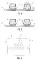
- FIG. 3is a side view of the chip in FIG. 2 after electroetching with a prior art etchant.
- FIG. 4is a side view of the chip in FIG. 3 after wet etching to remove the last layer of the seed layer.
- FIG. 5is an illustration of the surface of the chip in FIG. 4 showing incomplete etching of the seed layer.
- FIG. 6is a side view of the chip in FIG. 2 after electroetching with the etchant according to the present invention.
- FIG. 7is a side view of the chip in FIG. 6 after wet etching to remove the last layer of the seed layer.
- FIG. 8is an illustration of the surface of the chip in FIG. 7 showing complete etching of the seed layer.
- first chip 10comprised of semiconductor material 12 , seed layer 14 and solder bumps 24 .
- the seed layer 14is actually comprised of a plurality of layers.
- first layer 16 of a TiW alloye.g., 10 weight percent Ti and 90 weight percent Tungsten
- second layer 18of phased Cr/Cu or a Cr/Cu alloy
- third layer 20 of Cuthere may also be a barrier layer 22 of, for example, nickel.
- the solder bump 24 on chip 10comprises primarily Sn solder.
- Sn soldermight be be of moderate Sn content such as 60 weight percent or more Sn and 40 weight percent or less Pb, or high Sn content such as 95 weight percent or greater of Sn, balance Pb. Too, the solder may include lead-free alloys comprising primarily Sn such as Sn/Ag, Sn/Cu, Sn/Ag/Cu, and Sn/Bi alloys, just to name a few.
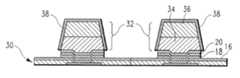
- Second chip 30comprised of semiconductor material 12 , seed layer 14 and solder bumps 32 .
- Seed layer 14could be the same as that shown in FIG. 1 or could be different, depending on the application.
- second chip 30could also have barrier layer 22 .
- Second chip 30contains solder bumps 32 .
- solder bumps 32comprise a solder hierarchical structure comprised of a higher melting temperature solder 34 and a lower melting temperature solder 36 .
- solder hierarchical structure shown in FIG. 2is for purposes of illustration only.
- Higher melting temperature solder 34could be a high Pb solder having 95 to 97 weight percent Pb, remainder Sn.
- Lower melting solder 36could be any of the moderate Sn content, high Sn content or lead-free alloys mentioned above.
- second chip 30has been electroetched with a conventional aqueous etchant including glycerol and potassium sulfate.
- a conventional aqueous etchantincluding glycerol and potassium sulfate.
- the composition of this etchantwas 1.5 M glycerol and 0.35 M K 2 SO 4 (potassium sulfate).
- the cell voltagewas 14.0 volts, the electrode spacing between the workpiece and the electrode was 3.0 mm, and the duty cycle was 20%.
- second chip 30was wet etched in a conventional aqueous etchant comprising 30% by weight hydrogen peroxide, 7.8 g/l K-EDTA and 1.1 M potassium sulfate for a period of 330 seconds.
- the bath temperaturewas set at 50° C.
- FIGS. 4 and 5The results after wet etching are illustrated in FIGS. 4 and 5 where it can be seen that the first layer 16 has been substantially removed leaving surface 42 of the second chip 30 mostly devoid of the first layer 16 .
- Sn deposits 39(as shown in FIG. 3) prevented the etching of some areas of first layer 16 , thereby leaving areas 40 of the first layer 16 which were not etched away.
- Chip structures such as that shown in FIGS. 3 to 5are undesirable and can result in high yield loss. As can be appreciated, any yield loss at this stage of the processing of the chip is very costly.
- second chip 30was electroetched with an aqueous etchant according to the present invention.
- the aqueous electrochemical etchant used for the present inventionwill have a composition comprising 1.30 to 1.70 M glycerol (HOCH 2 (OH)CH 2 OH) (preferably 1.5 M), 0 to 0.5 M sulfate ion concentration (preferably 0.35 M), and 0.1 to 0.5 M phosphate ion concentration (preferably 0.15 M).
- the pHshould be in the range of 4 to 9 (nominally 5), the cell voltage should be 13 to 17 V (nominally 14.5), the electrode spacing was 3.0 mm, and the duty cycle was 10 to 30% (preferably 20%).
- the sulfate ion and phosphate ionmay be derived from any salts. Among these are potassium sulfate and potassium phosphate but also sodium sulfate or sodium phosphate could be used for the purposes of the present invention.
- the relative amounts of sulfate ion and phosphate ionwould be adjusted based on the quantities of high Pb and high Sn solders present. If both high Pb and high Sn solders are present, both sulfate and phosphate ions must be present to protect the solders. If a high Pb solder is not present, the sulfate ions need not be present. As a minimum, the total amount of sulfate ions and phosphate ions must provide a high enough solution conductivity to perform the electroetch at a reasonable voltage.
- the metals that may be etched in the presence of the solder bumpsinclude titanium, tungsten, chromium, copper, nickel and alloys thereof.
- the metals that may be electroetched in the presence of the solder bumpsinclude a variety of metal stacks that include Cu, Cr/Cu, Cu/Ni, and Cr/Cu/Ni alloys.
- the etchant used to electroetch second chip 30comprised 1.5 M glycerol, 0.35 M K 2 SO 4 (potassium sulfate), and 0.15 M K 3 PO 4 (potassium phosphate).
- the pHwas adjusted to 5.0 using phosphoric acid.
- the cell voltagewas 14.0 volts, the electrode spacing was 3.0 mm, and the duty cycle was 20%.
- the whole of each of the solder bumpsis protected by crust 38 .
- second chip 30was wet etched in a conventional aqueous etchant comprising 30% by weight hydrogen peroxide, 7.8 g/l K-EDTA and 1.1 M potassium sulfate for a period of 330 seconds.
- the bath temperaturewas set at 50° C. The results are illustrated in FIGS. 7 and 8 where it can be seen that the first layer 16 has been entirely removed leaving surface 42 of the second chip 30 devoid of any residue.
- Protective crust 38remains in place after wet etching and is removed with methane sulfonic acid after wet etching is complete.
- the use of the present inventionhas been found to greatly increase the yield from the electroetching process.
Landscapes
- Engineering & Computer Science (AREA)
- Computer Hardware Design (AREA)
- Microelectronics & Electronic Packaging (AREA)
- Power Engineering (AREA)
- Chemical & Material Sciences (AREA)
- Manufacturing & Machinery (AREA)
- Chemical Kinetics & Catalysis (AREA)
- Materials Engineering (AREA)
- Electrochemistry (AREA)
- Metallurgy (AREA)
- Organic Chemistry (AREA)
- General Chemical & Material Sciences (AREA)
- Physics & Mathematics (AREA)
- Condensed Matter Physics & Semiconductors (AREA)
- General Physics & Mathematics (AREA)
- ing And Chemical Polishing (AREA)
- Weting (AREA)
- Preventing Corrosion Or Incrustation Of Metals (AREA)
Abstract
Description
Claims (21)
Priority Applications (5)
| Application Number | Priority Date | Filing Date | Title |
|---|---|---|---|
| US09/697,333US6468413B1 (en) | 2000-10-26 | 2000-10-26 | Electrochemical etch for high tin solder bumps |
| SG200106369ASG94868A1 (en) | 2000-10-26 | 2001-10-17 | Electrochemical etch for high tin solder bumps |
| JP2001323511AJP3368271B2 (en) | 2000-10-26 | 2001-10-22 | Selective electrochemical etching method and etchant used therefor |
| TW090126212ATW555886B (en) | 2000-10-26 | 2001-10-23 | Electrochemical etch for high tin solder bumps |
| CNB011371978ACN1184362C (en) | 2000-10-26 | 2001-10-25 | Electrochemical corrosion of high-tin solder bumps |
Applications Claiming Priority (1)
| Application Number | Priority Date | Filing Date | Title |
|---|---|---|---|
| US09/697,333US6468413B1 (en) | 2000-10-26 | 2000-10-26 | Electrochemical etch for high tin solder bumps |
Publications (1)
| Publication Number | Publication Date |
|---|---|
| US6468413B1true US6468413B1 (en) | 2002-10-22 |
Family
ID=24800725
Family Applications (1)
| Application Number | Title | Priority Date | Filing Date |
|---|---|---|---|
| US09/697,333Expired - LifetimeUS6468413B1 (en) | 2000-10-26 | 2000-10-26 | Electrochemical etch for high tin solder bumps |
Country Status (5)
| Country | Link |
|---|---|
| US (1) | US6468413B1 (en) |
| JP (1) | JP3368271B2 (en) |
| CN (1) | CN1184362C (en) |
| SG (1) | SG94868A1 (en) |
| TW (1) | TW555886B (en) |
Cited By (9)
| Publication number | Priority date | Publication date | Assignee | Title |
|---|---|---|---|---|
| US20020163084A1 (en)* | 2001-05-07 | 2002-11-07 | Tomonari Ohtsuki | Electronic component and process for manufacturing the same |
| US20040108367A1 (en)* | 2002-12-06 | 2004-06-10 | International Business Machines Corporation | Structure and method for lead free solder electronic package interconnections |
| US20050026450A1 (en)* | 2003-07-30 | 2005-02-03 | International Business Machines Corporation | Inhibition of tin oxide formation in lead free interconnect formation |
| US6876052B1 (en)* | 2000-05-12 | 2005-04-05 | National Semiconductor Corporation | Package-ready light-sensitive integrated circuit and method for its preparation |
| WO2005075711A1 (en)* | 2004-01-29 | 2005-08-18 | Applied Materials, Inc. | Method and composition for polishing a substrate |
| US20050208748A1 (en)* | 2004-03-17 | 2005-09-22 | International Business Machines Corporation | Method for forming robust solder interconnect structures by reducing effects of seed layer underetching |
| US7084064B2 (en) | 2004-09-14 | 2006-08-01 | Applied Materials, Inc. | Full sequence metal and barrier layer electrochemical mechanical processing |
| US7390744B2 (en) | 2004-01-29 | 2008-06-24 | Applied Materials, Inc. | Method and composition for polishing a substrate |
| US20230065692A1 (en)* | 2020-02-05 | 2023-03-02 | Texture Jet Ltd | Electrolyte Solution |
Families Citing this family (2)
| Publication number | Priority date | Publication date | Assignee | Title |
|---|---|---|---|---|
| CN110310939B (en)* | 2018-03-27 | 2021-04-30 | 矽品精密工业股份有限公司 | Substrate structure and manufacturing method thereof and conductive bump |
| CN111621787B (en)* | 2020-04-27 | 2022-07-12 | 江苏富乐华半导体科技股份有限公司 | Etching liquid system and method for etching aluminum nitride substrate |
Citations (6)
| Publication number | Priority date | Publication date | Assignee | Title |
|---|---|---|---|---|
| US4549944A (en)* | 1981-08-28 | 1985-10-29 | Hoechst Aktiengesellschaft | Electrochemical developing process for reproduction layers |
| US5318677A (en)* | 1991-02-13 | 1994-06-07 | Future Automation, Inc. | Process and solutions for removing resin bleed from electronic components |
| US5462638A (en) | 1994-06-15 | 1995-10-31 | International Business Machines Corporation | Selective etching of TiW for C4 fabrication |
| US5486282A (en) | 1994-11-30 | 1996-01-23 | Ibm Corporation | Electroetching process for seed layer removal in electrochemical fabrication of wafers |
| US5800726A (en) | 1995-07-26 | 1998-09-01 | International Business Machines Corporation | Selective chemical etching in microelectronics fabrication |
| US6015505A (en) | 1997-10-30 | 2000-01-18 | International Business Machines Corporation | Process improvements for titanium-tungsten etching in the presence of electroplated C4's |
- 2000
- 2000-10-26USUS09/697,333patent/US6468413B1/ennot_activeExpired - Lifetime
- 2001
- 2001-10-17SGSG200106369Apatent/SG94868A1/enunknown
- 2001-10-22JPJP2001323511Apatent/JP3368271B2/ennot_activeExpired - Fee Related
- 2001-10-23TWTW090126212Apatent/TW555886B/ennot_activeIP Right Cessation
- 2001-10-25CNCNB011371978Apatent/CN1184362C/ennot_activeExpired - Fee Related
Patent Citations (6)
| Publication number | Priority date | Publication date | Assignee | Title |
|---|---|---|---|---|
| US4549944A (en)* | 1981-08-28 | 1985-10-29 | Hoechst Aktiengesellschaft | Electrochemical developing process for reproduction layers |
| US5318677A (en)* | 1991-02-13 | 1994-06-07 | Future Automation, Inc. | Process and solutions for removing resin bleed from electronic components |
| US5462638A (en) | 1994-06-15 | 1995-10-31 | International Business Machines Corporation | Selective etching of TiW for C4 fabrication |
| US5486282A (en) | 1994-11-30 | 1996-01-23 | Ibm Corporation | Electroetching process for seed layer removal in electrochemical fabrication of wafers |
| US5800726A (en) | 1995-07-26 | 1998-09-01 | International Business Machines Corporation | Selective chemical etching in microelectronics fabrication |
| US6015505A (en) | 1997-10-30 | 2000-01-18 | International Business Machines Corporation | Process improvements for titanium-tungsten etching in the presence of electroplated C4's |
Cited By (19)
| Publication number | Priority date | Publication date | Assignee | Title |
|---|---|---|---|---|
| US7271029B1 (en) | 2000-05-12 | 2007-09-18 | National Semiconductor Corporation | Method of forming a package-ready light-sensitive integrated circuit |
| US6876052B1 (en)* | 2000-05-12 | 2005-04-05 | National Semiconductor Corporation | Package-ready light-sensitive integrated circuit and method for its preparation |
| US20020163084A1 (en)* | 2001-05-07 | 2002-11-07 | Tomonari Ohtsuki | Electronic component and process for manufacturing the same |
| US6818987B2 (en)* | 2001-05-07 | 2004-11-16 | Ddk Ltd. | Electronic component and process for manufacturing the same |
| US6854636B2 (en)* | 2002-12-06 | 2005-02-15 | International Business Machines Corporation | Structure and method for lead free solder electronic package interconnections |
| US20040108367A1 (en)* | 2002-12-06 | 2004-06-10 | International Business Machines Corporation | Structure and method for lead free solder electronic package interconnections |
| US6900142B2 (en) | 2003-07-30 | 2005-05-31 | International Business Machines Corporation | Inhibition of tin oxide formation in lead free interconnect formation |
| US20050026450A1 (en)* | 2003-07-30 | 2005-02-03 | International Business Machines Corporation | Inhibition of tin oxide formation in lead free interconnect formation |
| WO2005075711A1 (en)* | 2004-01-29 | 2005-08-18 | Applied Materials, Inc. | Method and composition for polishing a substrate |
| US7390744B2 (en) | 2004-01-29 | 2008-06-24 | Applied Materials, Inc. | Method and composition for polishing a substrate |
| US20090163019A1 (en)* | 2004-03-17 | 2009-06-25 | International Business Machines Corporation | Forming robust solder interconnect structures by reducing effects of seed layer underetching |
| US20050208748A1 (en)* | 2004-03-17 | 2005-09-22 | International Business Machines Corporation | Method for forming robust solder interconnect structures by reducing effects of seed layer underetching |
| US20060009022A1 (en)* | 2004-03-17 | 2006-01-12 | International Business Machines Corporation | Method for forming robust solder interconnect structures by reducing effects of seed layer underetching |
| US6995084B2 (en) | 2004-03-17 | 2006-02-07 | International Business Machines Corporation | Method for forming robust solder interconnect structures by reducing effects of seed layer underetching |
| US7767575B2 (en) | 2004-03-17 | 2010-08-03 | Tessera Intellectual Properties, Inc. | Forming robust solder interconnect structures by reducing effects of seed layer underetching |
| US7473997B2 (en) | 2004-03-17 | 2009-01-06 | International Business Machines Corporation | Method for forming robust solder interconnect structures by reducing effects of seed layer underetching |
| US7084064B2 (en) | 2004-09-14 | 2006-08-01 | Applied Materials, Inc. | Full sequence metal and barrier layer electrochemical mechanical processing |
| US7446041B2 (en) | 2004-09-14 | 2008-11-04 | Applied Materials, Inc. | Full sequence metal and barrier layer electrochemical mechanical processing |
| US20230065692A1 (en)* | 2020-02-05 | 2023-03-02 | Texture Jet Ltd | Electrolyte Solution |
Also Published As
| Publication number | Publication date |
|---|---|
| SG94868A1 (en) | 2003-03-18 |
| JP2002180299A (en) | 2002-06-26 |
| JP3368271B2 (en) | 2003-01-20 |
| CN1184362C (en) | 2005-01-12 |
| CN1354285A (en) | 2002-06-19 |
| TW555886B (en) | 2003-10-01 |
Similar Documents
| Publication | Publication Date | Title |
|---|---|---|
| US6015505A (en) | Process improvements for titanium-tungsten etching in the presence of electroplated C4's | |
| EP0687751B1 (en) | Selective etching of TiW for C4 fabrication | |
| US5937320A (en) | Barrier layers for electroplated SnPb eutectic solder joints | |
| US8314500B2 (en) | Interconnections for flip-chip using lead-free solders and having improved reaction barrier layers | |
| US7410833B2 (en) | Interconnections for flip-chip using lead-free solders and having reaction barrier layers | |
| US8003512B2 (en) | Structure of UBM and solder bumps and methods of fabrication | |
| KR100334593B1 (en) | Semiconductor device and method of the same | |
| EP1441388A2 (en) | Solder bump fabrication methods and structure including a titanium barrier layer | |
| US20030155408A1 (en) | Sacrificial seed layer process for forming c4 solder bumps | |
| KR20010098699A (en) | Method of forming lead-free bump interconnections | |
| JP2003007755A (en) | Barrier cap for lower bump metal | |
| US5646068A (en) | Solder bump transfer for microelectronics packaging and assembly | |
| US6468413B1 (en) | Electrochemical etch for high tin solder bumps | |
| US5800726A (en) | Selective chemical etching in microelectronics fabrication | |
| CN101668830A (en) | Selective etching of TiW for capture pad formation | |
| US11121101B2 (en) | Flip chip packaging rework | |
| US20020009869A1 (en) | Reflow of low melt solder tip C4's | |
| US7425278B2 (en) | Process of etching a titanium/tungsten surface and etchant used therein | |
| US5759437A (en) | Etching of Ti-W for C4 rework | |
| US20080119056A1 (en) | Method for improved copper layer etching of wafers with c4 connection structures | |
| JP3267167B2 (en) | Semiconductor device and manufacturing method thereof | |
| US6900142B2 (en) | Inhibition of tin oxide formation in lead free interconnect formation | |
| JP3506686B2 (en) | Method for manufacturing semiconductor device | |
| CN1103119C (en) | Method for Single Mask C4 Solder Bump Fabrication | |
| Datta | Flip-chip interconnection |
Legal Events
| Date | Code | Title | Description |
|---|---|---|---|
| AS | Assignment | Owner name:INTERNATINAL BUSINESS MACHINES CORPORATION, NEW YO Free format text:ASSIGNMENT OF ASSIGNORS INTEREST;ASSIGNORS:FANTI, LISA A.;COTTE, JOHN MICHAEL;EICHSTADT, DAVID ELY;REEL/FRAME:011271/0123;SIGNING DATES FROM 20001023 TO 20001025 | |
| STCF | Information on status: patent grant | Free format text:PATENTED CASE | |
| FPAY | Fee payment | Year of fee payment:4 | |
| FPAY | Fee payment | Year of fee payment:8 | |
| AS | Assignment | Owner name:ULTRATECH, INC., CALIFORNIA Free format text:ASSIGNMENT OF ASSIGNORS INTEREST;ASSIGNOR:INTERNATIONAL BUSINESS MACHINES CORPORATION;REEL/FRAME:028959/0001 Effective date:20120718 | |
| FEPP | Fee payment procedure | Free format text:PAT HOLDER CLAIMS SMALL ENTITY STATUS, ENTITY STATUS SET TO SMALL (ORIGINAL EVENT CODE: LTOS); ENTITY STATUS OF PATENT OWNER: SMALL ENTITY | |
| REFU | Refund | Free format text:REFUND - PAYMENT OF MAINTENANCE FEE, 12TH YEAR, LARGE ENTITY (ORIGINAL EVENT CODE: R1553); ENTITY STATUS OF PATENT OWNER: SMALL ENTITY | |
| FPAY | Fee payment | Year of fee payment:12 | |
| AS | Assignment | Owner name:VEECO INSTRUMENTS INC., NEW YORK Free format text:ASSIGNMENT OF ASSIGNORS INTEREST;ASSIGNOR:ULTRATECH, INC.;REEL/FRAME:051446/0476 Effective date:20191219 |