US6467413B1 - Method for marking a gambling chip by pad printing - Google Patents
Method for marking a gambling chip by pad printingDownload PDFInfo
- Publication number
- US6467413B1 US6467413B1US09/638,031US63803100AUS6467413B1US 6467413 B1US6467413 B1US 6467413B1US 63803100 AUS63803100 AUS 63803100AUS 6467413 B1US6467413 B1US 6467413B1
- Authority
- US
- United States
- Prior art keywords
- chip
- decoration
- pad
- section
- ink plate
- Prior art date
- Legal status (The legal status is an assumption and is not a legal conclusion. Google has not performed a legal analysis and makes no representation as to the accuracy of the status listed.)
- Expired - Lifetime
Links
Images


Classifications
- B—PERFORMING OPERATIONS; TRANSPORTING
- B41—PRINTING; LINING MACHINES; TYPEWRITERS; STAMPS
- B41F—PRINTING MACHINES OR PRESSES
- B41F17/00—Printing apparatus or machines of special types or for particular purposes, not otherwise provided for
- B41F17/001—Pad printing apparatus or machines
- A—HUMAN NECESSITIES
- A44—HABERDASHERY; JEWELLERY
- A44C—PERSONAL ADORNMENTS, e.g. JEWELLERY; COINS
- A44C21/00—Coins; Emergency money; Beer or gambling coins or tokens, or the like
Definitions
- the present inventionrelates to the marking of gambling chips having the general shape of a disc, or of objects of similar shape, by pad printing.
- Gambling chipalso called casino chip, should be understood to mean any element which can be used in gambling halls and represents a nominal value which may or may not be predetermined. Generally, these chips are manufactured from a rigid and scratch-resistant plastic.
- the term decorationshould be understood in its widest sense and it comprises, in particular, any drawing, symbol, mark and character (for example, letters, numbers, bar codes or various codings) capable of graphical representation and/or having a visual or optical effect (for example, by the use of U.V. -sensitive ink). More specifically, the decoration of the chips is capable of fulfilling at least one of the several functions presented briefly below:
- a decoration functionthe decoration having an aesthetic aspect and/or acting as an advertising medium
- a chip-authentication and security functionfor combatting the risk of falsification and/or the risk of fraudulent reproduction.
- Patent FR 2,730,392 in the name of the Applicantdescribes the use of pad printing for marking the surface of the faces and/or side of chips (as opposed to volume marking using multi-shot injection molding of variously colored plastics).
- this patentdescribes the marking of each face of the chip by pad printing using an inked pad which is moved coaxially with the chip with, for chips having a soft-profiled side without a straight side, marking of part of the side corresponding to the chamfered or rounded edge of the face of the chip.
- this techniquealthough satisfactory for the faces of the chip, is not always accepted by casinos for the side as it results in substantial modification of the profile of the side and/or in incomplete marking of the latter.
- the inventionrecognizes that there is a need for a new method of marking straight-sided gambling chips which eliminates, or appreciably reduces, the limitations and other drawbacks presented above.
- the inventionprovides a method of marking the side of a straight-sided disc-shaped gambling chip or an object of similar shape by pad printing, characterized by the use of an inked pad which is moved coaxially with the chip in conjunction with a flat ink plate having a ring-shaped zone suitable for being placed coaxially with the pad and bearing a decoration image defined by a radially deformed representation of the decoration of the straight side of the chip.
- the use of the decoration image which is radially deformed with respect to the side decorationmakes it possible to distribute the effect of distortion on the final decoration due to the variations in diameter of the chip over the entire circumferential perimeter of the side of the chip and to make this effect negligible.
- the decoration imageis obtained by the combination of an operation of radially folding up the decoration for the side of the chip around a facial edge included in the plane of the ink plate and of an operation of contracting the decoration towards the facial edge, the sequential or chronological order in which the two operations are performed being of no consequence,
- the decoration imageis obtained from an intermediate decoration produced by radially folding up the side decoration into a reference plane corresponding to the plane of the ink plate and including one of the faces of the chip (the reference face), by way of a radial transformation of contraction of the intermediate decoration in the reference plane towards the center of the ring bearing the decoration image.
- the position of the internal circular border of the ring and the contraction coefficient of the radial transformationare determined, for a given straight-sided chip model and a given pad, by marking the chip model using a positioning ink plate set on the axis of the chip and bearing a pattern consisting of closely-spaced concentric circles.
- the characteristics of the radial contraction transformationare chosen in order to obtain a reduction in the radial height of the intermediate decoration (equal in height to the side decoration) of between 25 and 40%, i.e. a radial contraction coefficient of between 0.75 and 0.6.
- the magnitude of the radial contraction and of the associated reduction in height of the side decorationdepend on the deformation of the pad on the surface of the chip, in other words they depend on the type of chip to be marked, on the profile and nature of the pad (material, hardness, surface finish) and, to a lesser extent, on the inks employed.
- an ink plate having a halftone decoration image for a face of the chip and a non-halftone side decoration imageor an ink plate having a decoration image for a face of the chip and a deeply-etched side decoration image, the etching of the side decoration image then being deeper than the etching of the decoration image for the face of the chip.
- the heightwise positioning of the decorationis facilitated for marking a solid-straight-sided chip.
- the inventionalso applies to soft-edged chips having a central straight side extending substantially over a large portion of the thickness of the chip and connected to the two faces of the latter by two transition zones (small fillets or broadened chamfers).
- these central-straight-sided chipsare marked by making the internal circular border of the ring to correspond approximately to the circle of axial projection of the straight side on the reference face of the chip.
- an axially symmetric deformable padwhich has a diameter at least equal to the diameter of the chip increased by about five times the height of the side of the chip.
- the inventionalso relates to a pad-printing device suitable for implementing this method, which includes a support for the chip, the support being equipped with a mechanism for centering the chip coaxially with the pad before the operation of marking the side by pad printing, the centering mechanism being retractable in order to allow the side of the chip to be marked during movement of the pad.
- the retractable centering mechanismsof the type comprising slides or a centering ring, are mounted so as to slide axially over the perimeter of the support.
- the device accordingly to the inventionincludes a mechanism for holding the chip in place on its support, especially when raising the pad.
- the mechanism for holding the chip in placeincludes at least one adhesive patch, in contact with that face of the chip which bears on the support, and/or of suction under vacuum.
- FIG. 1shows a perspective view of a solid-straight-sided gambling chip with a side decoration
- FIG. 2shows a plan view of the ink plate used for producing the side decoration for the chip of FIG. 1 using the method of the invention
- FIG. 3is a diagram showing the principle of operation of a pad-printing apparatus allowing implementation of the method of the invention
- FIGS. 4 a and 4 bshow an operation of marking the side of a straight-sided gambling chip by pad printing using the device illustrated in FIG. 3;
- FIG. 5shows an enlarged sectional diagrammatic view of a central-straight-sided gambling chip and of the corresponding ink plate used for decorating the straight side of the chip using the method of the invention.
- FIG. 1shows, in perspective, a gambling chip 10 made of plastic (for example made of polybutylene terephthalate PBT) having the general shape of a disc with parallel faces 12 and 13 and a solid straight side 14 .
- the surface of the straight side 14is in the form of a right cylinder of axis ZZ′ perpendicular to the faces of the chip (of height approximately equal to the thickness of the chip), this cylinder being bounded with respect to the faces by right-angled edges 16 and 17 .
- the chip 10has a diameter of 40 mm for a side thickness or height of about 3.3 mm, it being pointed out that, in some cases, the edges 16 and 17 may have a very slight chamfer (of about 0.1 mm), this having the effect in particular, of extending the life of the pad.
- the upper face 12 and its edge 16both lie in the XX′,YY′ plane perpendicular to the ZZ′ axis, this plane being chosen by convention as the reference plane Pref corresponding to the plane of the ink plate 11 (the origin O being chosen as the intersection of the three axes).
- the side 14has a side decoration, in this case, and by way of non-limiting example, a crenellated line 15 consisting of sixteen symmetrical crenels distributed around the circumferential perimeter of the chip 10 , the crenellated line 15 being moreover centered heightwise on the side 14 .
- FIG. 2shows the drawing of the flat ink plate 11 corresponding to the upper face 12 and to the side 14 of the chip 10 and constructed directly in the reference plane Pref.
- the face 12reference face
- a face decorationfor example a colored square 18
- the side decoration 15is shown, to size, as the edge 16 (the reference edge) represented by a first dashed circle.
- the decoration image 22 for the side line 15appears in the form of a crenellated circular curve between the two circles 16 and 17 ′.
- the decoration image 22is obtained by radially deforming the side decoration line 15 , preferably in the following manner.
- the face 12is firstly divided by a certain number of radii OR into equal sectors, tie angle of which, at the center, between two successive radii OR(i) and OR(i+1), is chosen according to the definition desired for the decoration image (in this case, a sector having an angle of 11.25 degrees at the center is sufficient to cover each crenel of the decoration 15 ).
- the points A 0 , A 1 , A 2 , A 3 , A 4 , A 5 , A 6 , A 7 and A 8 in FIGS. 1 and/or 2indicate the respective points of intersection of the edge 16 of the upper face 12 with the corresponding radius OR(i), as can be seen, for instance, in FIG. 1 at A 7 on radius OR 7 .
- the points A(i) on the upper edge 16 of the cylinder-shaped chip 10have corresponding ones B(i) at the intersection of the cylinder generatfices with the lower edge 17 of the lower face (not shown) of the chip 10 , as can be seen, for instance, at A 0 , B 0 or A 7 , B 7 .
- each radial plane PR defined by the ZZ′ axis and a radius OR(for example the plane PR 7 with the radius OR 7 )
- the generatrix defined by the intersection of the radial plane PR (in this case, the plane PR 7 ) with the cylindrical side 14 of the chip(in this case, the generatrix A 7 B 7 ) is radially folded up onto the reference plane Pref by rotating it through 90 degrees about the corresponding point of intersection A of the edge 16 with the radius OR (in this case, the point A 7 ).
- the image point B′ 7 of the point B 7 and all the folded-up intermediate points (in this case, the segment C′ 7 D′ 7 ) of the points of the original decoration 15 which lie along the generatrix A 7 B 7 (in this case, the segment C 7 D 7 )are constructed on the radius OR 7 .
- the image circle 17 ′ of the edge 17 and the intermediate decoration 15 ′which is in the form of a crenellated circle (partially illustrated by the dotted line in FIG. 2 ), are constructed, point by point, in the reference plane Pref, i.e. on each radius OR, and radius after radius.
- This radial folding-up operationis followed by a radial transformation in which the intermediate decoration 15 ′ (illustrated by the moving point P′) is contracted towards the internal circular border of the ring 20 (the edge 16 ), the point-by-point radial movement in the reference plane along each radius OR usually resulting in a reduction in the radial width (or height) of the intermediate decoration 15 ′ (equal to the height of the decoration 15 ) in order to end up, in the reference plane, with the definitive decoration image 22 on the ink plate (illustrated by the moving point P′′).
- the contraction coefficient K for the height of the side decoration 15is between 0.75 and 0.60, which gives a reduction in the height of the decoration of between 25 and 40%.
- the magnitude of the total radial displacement P′P′′ towards the edge 16 of each intermediate point P′ lying on the segment AB′ of a radius ORis greater the further the point P′ is from the point A.
- the gambling chipmay be replaced by an object of similar shape made of a material capable of receiving a decoration by pad printing.
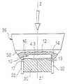
- FIG. 3illustrates the principle of such an apparatus for implementing the invention, allowing one of the faces and the side of a disc-shaped gambling chip or of an object of similar shape to be marked simultaneously.
- the reference 30represents a horizontal support intended to act as a bearing surface for the solid-straight-sided chip 10 .
- An ink pad 34is mounted on a frame 31 so as to be able to move in vertical reciprocating motion.
- the pad 34has an axially symmetrical deformable head 36 of axis ZZ′ made of synthetic material (for example a synthetic silicone rubber having a Shore A hardness of about 6), in this case with a conical end 38 .
- the deformable head 36is designed to bed down on the face 12 and the edge 16 of the chip 10 while the straight side 14 is being marked.
- a plate holder 40carrying a flat ink plate 11 which incorporates the image of a side decoration (for example the decoration image 22 illustrated in FIG.
- the pad-printing operationis carried out in the following manner. After inking the plate 11 (position 40 ′), the plate holder 40 is moved into the position 40 coaxial with the pad 34 so as to place the ring-shaped zone 20 of the plate 11 coaxially with the pad 34 . A first downward vertical movement of the pad 34 allows the ink to be picked up simply by applying pressure.
- the pad 34After the pad 34 has been raised and the plate holder 40 retracted (back to the position 40 ′), the pad 34 undergoes a second downward vertical movement in order to deposit the ink firstly by pressing on the face 12 of the chip 10 and then, by further deformation of the head of the pad 36 , on the side 14 . Marking with a monochrome (final or intermediate) decoration is thus achieved.
- the final decorationis formed by a complementarity and/or superposition of monochrome decorations, each of these intermediate decorations being etched on separate plates.
- multicolor markingeither several movable plate holders or a series of monochrome pad-printing units associated with a movable chip-holder support are used.
- the ink platesare etched to a depth of between 18 and 20 micrometers.
- the various types of inks and/or varnishes suitable for pad printingcan be used, especially UV-visible inks for discreet marking (for example in the case of chip identification numbers and/or codings).
- an ink platehaving a decoration image for a face of the chip and a deeply-etched side decoration image, the etching of the side decoration image (about 25 micrometers) then being deeper than the etching of the decoration image for the face of the chip (about 18 micrometers).
- a plateis obtained by using a suitable mask.
- the chipis centered on the ZZ′ axis of the pad by retractable vertical centering slides 32 having curved internal walls complementas with the side 14 of the chip 10 and being mounted so as to slide axially on the perimeter of the support 30 .
- This centering operationprior to the marking proper or in the initial phase of the marking, is important in order to position the chip 10 accurately with respect to the pad 34 , especially in the present case so that the edge 16 is in precise correspondence with its inked image on the conical end 38 of the pad 34 .
- the centering slides 32gradually retract (by way of any known mechanical arrangement) in order to allow the head 38 of the pad 34 to deform along the side 14 , while bedding down on the edge 16 (the latter being sufficiently sharp to prevent undesirable slippage from the face 12 in the region of the edge) until complete inking of the side 14 when the end 38 (which is conical when not in use) of the deformable head 36 of the pad 34 is compressed (with the rim of the head 36 projecting slightly beyond the plane of the edge 17 of the lower face 13 of the chip 10 ).
- a mechanismfor holding the chip 10 in place on its support 30 , for example at least one adhesive patch 43 fixed to the support 30 , the patch 43 being in contact with the lower face 13 of the chip 10 bearing on the support 30 , and/or suction under partial vacuum (not shown).
- the use of one or more patches 43 providing sufficient adhesion to ensure, once the chip has been centered by the slides 32 , that the chip is held in place while it is being marked.makes it possible to retract the slides 32 even before the actual marking of the chip 10 .
- the slides 32may be replaced by a retractable ring (not shown) mounted on the perimeter of the chip support 30 .
- the pad 34has a deformable head 36 with a substantially conical end and with a working diameter Dt at least equal to the diameter of the chip increased by five times the height of the side of the chip, for example a minimum diameter Dt of 55 mm for the chip 10 with a diameter of 40 mm and a side height h of 3.3 mm.
- the inventioncan be used with other types of pads, of various shapes and of various hardnesses, chosen from the manufacturers' standard ranges. Among these may be mentioned pads of cylindrical shape with a convex end, the diameter Dt of which satisfies the above criterion.
- the inventionalso applies to soft-edged chips having a central straight side extending substantially over a large portion of the thickness of the chip and connected to the two faces of the latter by two transition zones (small fillets or broadened chamfers).
- the chip 60 shown diagrammatically in FIG. 5has a diameter of 40 mm for a total side height of 3.3 mm, consisting of approximately 2.5 mm of central straight side and of two transition fillets having a radius of between 0.4 and 0.5 mm (with a theoretical radius in the injection mould of 0.5 mm).
- the invention as described by way of non-limiting example for the solid-straight-sided chip 10in particular the marking operations proper and its various variants, the marking device and its variants, the various pads, the general principle of preparing the plates by folding up onto the reference plane and radially contracting the intermediate decoration, and the plate-etching variants, is also applicable to a central-straight-sided chip, especially to the chip 60 illustrated in FIG. 5 .
- the softened edge of the chipleads to slippage of the pad in the region of the softened edge which often requires making a correction to the placement of the internal border of the ring bearing the decoration image and, possibly, to the contraction coefficient K.
- the internal border of the ring 70 bearing the decoration imageis generally moved closer to the center O of the chip 10 .
- FIG. 5shows, in diagrammatic cross-section, the chip 60 of axis ZZ′ with its reference face 62 of center O included in the reference plane Pref (half-axis OX) corresponding to the flat ink plate 61 , the peripheral circular border of the face 62 being shown by the point E.
- Prefhalf-axis OX
- the straight side of the chip 60includes a straight side 64 (comprising a cylindrical surface of axis ZZ′ perpendicular to the plane Pref, which, projected on to the latter forms a circle of radius OJ and is represented by the segment FG) and of two transition zones, in this case two fillets 66 and 66 ′ (comprising surfaces of revolution having the general shape of a spherical ring or of a cone and represented by the circular quadrants EF and GH, the point H on the other face 63 of the chip 60 being the equivalent of the point E on the face 62 ).
- a straight side 64comprising a cylindrical surface of axis ZZ′ perpendicular to the plane Pref, which, projected on to the latter forms a circle of radius OJ and is represented by the segment FG
- two fillets 66 and 66 ′comprising surfaces of revolution having the general shape of a spherical ring or of a cone and represented by the circular quadrants EF and
- the position of the internal circular border of the ring 70 and the contraction coefficient K of the radial transformationare determined, for a given model of straight-sided chip (for example, the chip 60 having a side profile EFGH) and for a given pad, by marking the chip model using a positioning ink plate 80 centered on the axis ZZ′ of the clip and bearing a pattern 82 consisting of closely-spaced concentric circles.
- the pattern 82shown diagrammatically in FIG.
- the pattern 82 used for the chip 60has 23 closely-spaced concentric circles 84 numbered from M 1 to M 23 and, in this case, spaced apart by 0.3 mm for a pattern width of about 7 mm.
- the patternhas segments (not shown) of 64 equally distributed radii crossing the concentric circles 84 in order to determine the lateral broadening of the decoration image with the distance from the center O and to detect any possible lateral slippage of the pad.
- the positioning plate 80is used to mark the straight side of the model of the chip 60 .
- the row of the concentric circles Mi and Me corresponding to the points F′′ and G′′(in this case, the row 12 and the row 17 , respectively illustrated by the circles M 12 and M 17 ) are identified by counting along the marked chip.
- the central straight side of the chip 60is marked by pad printing by using, in a manner already described, the device illustrated in FIGS. 3, 4 a and 4 b (the chip 60 replacing the chip 10 ).
Landscapes
- Printing Methods (AREA)
- Absorbent Articles And Supports Therefor (AREA)
- Auxiliary Devices For And Details Of Packaging Control (AREA)
- Labeling Devices (AREA)
- Control Of Vending Devices And Auxiliary Devices For Vending Devices (AREA)
- Dot-Matrix Printers And Others (AREA)
- Inks, Pencil-Leads, Or Crayons (AREA)
- Image Analysis (AREA)
- Pinball Game Machines (AREA)
Abstract
Description
Claims (4)
Applications Claiming Priority (2)
| Application Number | Priority Date | Filing Date | Title |
|---|---|---|---|
| FR9703872 | 1997-03-28 | ||
| FR9703872AFR2761297B1 (en) | 1997-03-28 | 1997-03-28 | METHOD FOR TAMPOGRAPHIC MARKING OF A GAME TOKEN AND DEVICE FOR IMPLEMENTING THE METHOD |
Related Parent Applications (2)
| Application Number | Title | Priority Date | Filing Date |
|---|---|---|---|
| PCT/FR1998/000485ContinuationWO1998043816A1 (en) | 1997-03-28 | 1998-03-11 | Method for marking a gaming disk by pad printing and device for implementing same |
| US09/147,253ContinuationUS6176185B1 (en) | 1997-03-28 | 1998-03-11 | Method for marking a gaming disk by pad printing |
Publications (1)
| Publication Number | Publication Date |
|---|---|
| US6467413B1true US6467413B1 (en) | 2002-10-22 |
Family
ID=9505323
Family Applications (2)
| Application Number | Title | Priority Date | Filing Date |
|---|---|---|---|
| US09/147,253Expired - Fee RelatedUS6176185B1 (en) | 1997-03-28 | 1998-03-11 | Method for marking a gaming disk by pad printing |
| US09/638,031Expired - LifetimeUS6467413B1 (en) | 1997-03-28 | 2000-08-15 | Method for marking a gambling chip by pad printing |
Family Applications Before (1)
| Application Number | Title | Priority Date | Filing Date |
|---|---|---|---|
| US09/147,253Expired - Fee RelatedUS6176185B1 (en) | 1997-03-28 | 1998-03-11 | Method for marking a gaming disk by pad printing |
Country Status (11)
| Country | Link |
|---|---|
| US (2) | US6176185B1 (en) |
| EP (1) | EP0973642B1 (en) |
| AT (1) | ATE217579T1 (en) |
| AU (1) | AU6841498A (en) |
| CA (1) | CA2256551C (en) |
| DE (1) | DE69805405T2 (en) |
| ES (1) | ES2176998T3 (en) |
| FR (1) | FR2761297B1 (en) |
| PT (1) | PT973642E (en) |
| WO (1) | WO1998043816A1 (en) |
| ZA (1) | ZA982598B (en) |
Cited By (12)
| Publication number | Priority date | Publication date | Assignee | Title |
|---|---|---|---|---|
| US20020185019A1 (en)* | 2001-06-06 | 2002-12-12 | Etablissements Bourgogne Et Grasset | Chip holding arrangement, pad printing system incorporating the arrangement, and method of pad pringting a chip using the arrangement |
| US20030218299A1 (en)* | 2002-05-22 | 2003-11-27 | The Bud Jones Company, Inc. | Method of manufacturing gaming dice and die made thereby |
| US20040014838A1 (en)* | 2002-07-22 | 2004-01-22 | Etablissements Bourgogne Et Grasset | Method for marking by pad-printing and sublimation, and sublimable pad-printing inks |
| US20040087375A1 (en)* | 2001-12-03 | 2004-05-06 | Emmanuel Gelinotte | Electronic device for gaming chips |
| US20040229682A1 (en)* | 2003-05-12 | 2004-11-18 | Etablissements Bourgogne Et Grasset | Station for reading and/or writing in electronic gaming chips |
| US20070105616A1 (en)* | 2005-11-09 | 2007-05-10 | Gamiong Partners International | Chip with insert including an electronic microchip |
| US20070167134A1 (en)* | 2005-04-07 | 2007-07-19 | Gaming Partners International. Of Savigny-Les- Be Aune | Method of managing a plurality of electronic microcircuit chip readers and equipments for implementing said method |
| US20070278314A1 (en)* | 2005-07-08 | 2007-12-06 | Pierre Chapet | Electronic Microchip Token And Its Fabrication Process |
| US20090146373A1 (en)* | 2007-05-25 | 2009-06-11 | Pierre Chapet | Token With Electronic Device, Method of Making Thereof, and Apparatus for Making Thereof |
| CN103753948A (en)* | 2012-05-09 | 2014-04-30 | 南京乐金熊猫电器有限公司 | Pad printing device |
| CN106541698A (en)* | 2017-01-03 | 2017-03-29 | 深圳市裕同包装科技股份有限公司 | A kind of printing equipment and its operational approach of side automatic colouring |
| CN114222664A (en)* | 2019-07-17 | 2022-03-22 | 皮埃斯产业有限公司 | Display panel side terminal printing system |
Families Citing this family (13)
| Publication number | Priority date | Publication date | Assignee | Title |
|---|---|---|---|---|
| US20030174864A1 (en)* | 1997-10-27 | 2003-09-18 | Digital Biometrics, Inc. | Gambling chip recognition system |
| US6532297B1 (en)* | 1995-10-05 | 2003-03-11 | Digital Biometrics, Inc. | Gambling chip recognition system |
| FR2761297B1 (en) | 1997-03-28 | 1999-05-21 | Bourgogne Grasset | METHOD FOR TAMPOGRAPHIC MARKING OF A GAME TOKEN AND DEVICE FOR IMPLEMENTING THE METHOD |
| BE1013128A6 (en)* | 1999-09-21 | 2001-10-02 | Volder L De | Device for printing objects of the type of tablets with special medical tablets. |
| DE10003412A1 (en)* | 2000-01-27 | 2001-08-02 | Hermann Lutz | Method for surface finishing and refining three-dimensional wooden curtain rings, involves initially printing on one side of the ring and then on the other side in a two-step process |
| FR2805067B1 (en)* | 2000-02-15 | 2003-09-12 | Bourgogne Grasset | ELECTRONIC CHIP TOKEN AND METHODS OF MANUFACTURING SUCH A TOKEN |
| DE202006020754U1 (en)* | 2006-02-03 | 2010-01-07 | Itw Morlock Gmbh | Pad printing plant |
| AU2008252054A1 (en)* | 2007-12-18 | 2009-07-02 | Aristocrat Technologies Australia Pty Limited | A gaming machine and a network of gaming machines |
| EP2546058B1 (en)* | 2010-03-12 | 2019-05-29 | Mimaki Engineering Co., Ltd. | Imaging device and imaging method |
| CN106696452B (en)* | 2017-01-03 | 2022-09-27 | 深圳市裕同包装科技股份有限公司 | Die cutting and coloring integrated equipment and processing method for die cutting and coloring paper |
| EP3598920A1 (en)* | 2018-07-26 | 2020-01-29 | Trisa Holding AG | Marking/printing on method for application and/or cleansing elements |
| KR20210011524A (en)* | 2019-07-22 | 2021-02-02 | 삼성디스플레이 주식회사 | Pad printing device |
| US11717728B1 (en)* | 2022-02-28 | 2023-08-08 | Acushnet Company | Golf ball having markings spaced from a centerline plane |
Citations (10)
| Publication number | Priority date | Publication date | Assignee | Title |
|---|---|---|---|---|
| US2748696A (en) | 1951-06-13 | 1956-06-05 | Murray Lilian | Printing or decoration of ceramic or other ware |
| US3868902A (en) | 1972-07-29 | 1975-03-04 | Service Eng Ltd | Multi-station printing machine for ceramic ware |
| US4019436A (en) | 1976-06-16 | 1977-04-26 | Martin Handweiler | Technique for producing a pre-distorted design format for use in transfer printing |
| FR2463683A1 (en) | 1979-08-23 | 1981-02-27 | Essilor Int | Transfer pad for adding decorative transfer to spectacle frame - has transfer profile applied by pressure of ridge of elastic pad on frame mounted on fixed base |
| WO1987000796A1 (en) | 1985-07-31 | 1987-02-12 | Unice, S.A. | Device for printing spherical objects and the like |
| US5165340A (en) | 1991-03-06 | 1992-11-24 | Karlyn William M | Multicolor printing system for the silk-screen printing of compact discs |
| EP0581378A1 (en) | 1992-07-31 | 1994-02-02 | O.M.S.O. S.P.A. | Machine for the offset printing of flat objects, in particular for compact discs |
| FR2730392A1 (en) | 1995-02-15 | 1996-08-14 | Bourgogne Grasset | GAME TOKEN AND METHOD FOR MARKING SUCH A TOKEN |
| WO1998043816A1 (en) | 1997-03-28 | 1998-10-08 | Etablissements Bourgogne Et Grasset | Method for marking a gaming disk by pad printing and device for implementing same |
| FR2774326A1 (en) | 1998-01-30 | 1999-08-06 | Kammann Maschf Werner | DEVICE FOR DECORATING OBJECTS |
Family Cites Families (2)
| Publication number | Priority date | Publication date | Assignee | Title |
|---|---|---|---|---|
| JPS6030344A (en)* | 1983-07-29 | 1985-02-15 | M G:Kk | Manufacture of key top |
| JP2838203B2 (en)* | 1987-05-13 | 1998-12-16 | 一兄 加藤 | Method and apparatus for painting bowl-shaped articles |
- 1997
- 1997-03-28FRFR9703872Apatent/FR2761297B1/ennot_activeExpired - Fee Related
- 1998
- 1998-03-11EPEP98913882Apatent/EP0973642B1/ennot_activeExpired - Lifetime
- 1998-03-11DEDE69805405Tpatent/DE69805405T2/ennot_activeExpired - Lifetime
- 1998-03-11USUS09/147,253patent/US6176185B1/ennot_activeExpired - Fee Related
- 1998-03-11AUAU68414/98Apatent/AU6841498A/ennot_activeAbandoned
- 1998-03-11ATAT98913882Tpatent/ATE217579T1/ennot_activeIP Right Cessation
- 1998-03-11ESES98913882Tpatent/ES2176998T3/ennot_activeExpired - Lifetime
- 1998-03-11CACA002256551Apatent/CA2256551C/ennot_activeExpired - Fee Related
- 1998-03-11PTPT98913882Tpatent/PT973642E/enunknown
- 1998-03-11WOPCT/FR1998/000485patent/WO1998043816A1/enactiveIP Right Grant
- 1998-03-27ZAZA982598Apatent/ZA982598B/enunknown
- 2000
- 2000-08-15USUS09/638,031patent/US6467413B1/ennot_activeExpired - Lifetime
Patent Citations (13)
| Publication number | Priority date | Publication date | Assignee | Title |
|---|---|---|---|---|
| US2748696A (en) | 1951-06-13 | 1956-06-05 | Murray Lilian | Printing or decoration of ceramic or other ware |
| US3868902A (en) | 1972-07-29 | 1975-03-04 | Service Eng Ltd | Multi-station printing machine for ceramic ware |
| US4019436A (en) | 1976-06-16 | 1977-04-26 | Martin Handweiler | Technique for producing a pre-distorted design format for use in transfer printing |
| FR2463683A1 (en) | 1979-08-23 | 1981-02-27 | Essilor Int | Transfer pad for adding decorative transfer to spectacle frame - has transfer profile applied by pressure of ridge of elastic pad on frame mounted on fixed base |
| WO1987000796A1 (en) | 1985-07-31 | 1987-02-12 | Unice, S.A. | Device for printing spherical objects and the like |
| US5165340A (en) | 1991-03-06 | 1992-11-24 | Karlyn William M | Multicolor printing system for the silk-screen printing of compact discs |
| EP0581378A1 (en) | 1992-07-31 | 1994-02-02 | O.M.S.O. S.P.A. | Machine for the offset printing of flat objects, in particular for compact discs |
| FR2730392A1 (en) | 1995-02-15 | 1996-08-14 | Bourgogne Grasset | GAME TOKEN AND METHOD FOR MARKING SUCH A TOKEN |
| US5794532A (en) | 1995-02-15 | 1998-08-18 | Etablissements Bourgogne Et Grasset | Gambling chip and method of marking same |
| WO1998043816A1 (en) | 1997-03-28 | 1998-10-08 | Etablissements Bourgogne Et Grasset | Method for marking a gaming disk by pad printing and device for implementing same |
| US6176185B1 (en) | 1997-03-28 | 2001-01-23 | Etablissements Bourgogne Et Grasset | Method for marking a gaming disk by pad printing |
| FR2774326A1 (en) | 1998-01-30 | 1999-08-06 | Kammann Maschf Werner | DEVICE FOR DECORATING OBJECTS |
| US6148721A (en) | 1998-01-30 | 2000-11-21 | Werner Kammann Maschinenfabrik Gmbh | Apparatus for decorating articles using suction conveyor |
Non-Patent Citations (2)
| Title |
|---|
| Patent Abstracts of Japan, vol. 13, No. 83 (M-802) for JP 63-280639A, Feb. 27, 1989. |
| Patent Abstracts of Japan, vol. 9, No. 152 (M-391) for JP 60-030344, Feb. 15, 1985. |
Cited By (23)
| Publication number | Priority date | Publication date | Assignee | Title |
|---|---|---|---|---|
| US20020185019A1 (en)* | 2001-06-06 | 2002-12-12 | Etablissements Bourgogne Et Grasset | Chip holding arrangement, pad printing system incorporating the arrangement, and method of pad pringting a chip using the arrangement |
| US7100501B2 (en)* | 2001-06-06 | 2006-09-05 | Gaming Partners International | Chip holding arrangement, pad printing system incorporating the arrangement, and method of pad printing a chip using the arrangement |
| US20040087375A1 (en)* | 2001-12-03 | 2004-05-06 | Emmanuel Gelinotte | Electronic device for gaming chips |
| US20030218299A1 (en)* | 2002-05-22 | 2003-11-27 | The Bud Jones Company, Inc. | Method of manufacturing gaming dice and die made thereby |
| US7563834B2 (en) | 2002-07-22 | 2009-07-21 | Gaming Partners International | Sublimable pad-printing inks |
| US20040014838A1 (en)* | 2002-07-22 | 2004-01-22 | Etablissements Bourgogne Et Grasset | Method for marking by pad-printing and sublimation, and sublimable pad-printing inks |
| US20060027118A1 (en)* | 2002-07-22 | 2006-02-09 | Gaming Partners International Of Savigny | Sublimable pad-printing inks |
| US7063012B2 (en) | 2002-07-22 | 2006-06-20 | Gaming Partners International | Method for marking by pad-printing and sublimation, and sublimable pad-printing inks |
| US7883408B2 (en) | 2003-05-12 | 2011-02-08 | Gaming Partners International | Station for reading and/or writing in electronic gaming chips |
| US20040229682A1 (en)* | 2003-05-12 | 2004-11-18 | Etablissements Bourgogne Et Grasset | Station for reading and/or writing in electronic gaming chips |
| US7382229B2 (en) | 2005-04-07 | 2008-06-03 | Gaming Partners International | Method of managing a plurality of electronic microcircuit chip readers and equipments for implementing said method |
| US20070167134A1 (en)* | 2005-04-07 | 2007-07-19 | Gaming Partners International. Of Savigny-Les- Be Aune | Method of managing a plurality of electronic microcircuit chip readers and equipments for implementing said method |
| US20070278314A1 (en)* | 2005-07-08 | 2007-12-06 | Pierre Chapet | Electronic Microchip Token And Its Fabrication Process |
| US7931204B2 (en) | 2005-07-08 | 2011-04-26 | Gaming Partners International | Electronic microchip token and its fabrication process |
| US7918455B2 (en) | 2005-11-09 | 2011-04-05 | Gaming Partners International | Chip with insert including an electronic microchip |
| US20070105616A1 (en)* | 2005-11-09 | 2007-05-10 | Gamiong Partners International | Chip with insert including an electronic microchip |
| US20090146373A1 (en)* | 2007-05-25 | 2009-06-11 | Pierre Chapet | Token With Electronic Device, Method of Making Thereof, and Apparatus for Making Thereof |
| US7866563B2 (en) | 2007-05-25 | 2011-01-11 | Gaming Partners International | Token with electronic device, method of making thereof, and apparatus for making thereof |
| CN103753948A (en)* | 2012-05-09 | 2014-04-30 | 南京乐金熊猫电器有限公司 | Pad printing device |
| CN103753948B (en)* | 2012-05-09 | 2016-08-17 | 南京乐金熊猫电器有限公司 | Printer device |
| CN106541698A (en)* | 2017-01-03 | 2017-03-29 | 深圳市裕同包装科技股份有限公司 | A kind of printing equipment and its operational approach of side automatic colouring |
| CN114222664A (en)* | 2019-07-17 | 2022-03-22 | 皮埃斯产业有限公司 | Display panel side terminal printing system |
| CN114222664B (en)* | 2019-07-17 | 2024-04-09 | 株式会社皮埃斯爱 | Display panel side terminal printing system |
Also Published As
| Publication number | Publication date |
|---|---|
| CA2256551C (en) | 2006-08-29 |
| DE69805405D1 (en) | 2002-06-20 |
| FR2761297B1 (en) | 1999-05-21 |
| WO1998043816A1 (en) | 1998-10-08 |
| EP0973642A1 (en) | 2000-01-26 |
| DE69805405T2 (en) | 2003-01-09 |
| ZA982598B (en) | 1998-04-15 |
| AU6841498A (en) | 1998-10-22 |
| PT973642E (en) | 2002-09-30 |
| ES2176998T3 (en) | 2002-12-01 |
| US6176185B1 (en) | 2001-01-23 |
| CA2256551A1 (en) | 1998-10-08 |
| FR2761297A1 (en) | 1998-10-02 |
| EP0973642B1 (en) | 2002-05-15 |
| ATE217579T1 (en) | 2002-06-15 |
Similar Documents
| Publication | Publication Date | Title |
|---|---|---|
| US6467413B1 (en) | Method for marking a gambling chip by pad printing | |
| US5794532A (en) | Gambling chip and method of marking same | |
| US11794468B2 (en) | Device for printing cans, a process for printing cans, a printed can and a transfer blanket | |
| US5882555A (en) | Apparatus and method for manufacturing compact discs having a non-round outer profile | |
| RU2183558C2 (en) | Stamp manufacture method | |
| ES2964224T3 (en) | Printing procedures for metal bodies of beverage containers | |
| JP3072921B2 (en) | Pneumatic tire | |
| TW298574B (en) | ||
| US20150183211A1 (en) | Method and Apparatus For Printing Cans | |
| US5505125A (en) | Method and apparatus for forming a rotary embossing die with a support plate | |
| CN109715404B (en) | Can embossing apparatus and related method | |
| EP3115215A1 (en) | Method for making a colored contact lens | |
| US3634951A (en) | Molded relief sheets | |
| JP6859070B2 (en) | Printing blanket | |
| US3458614A (en) | Method for the manufacture of molded composite relief sheets | |
| US20030218299A1 (en) | Method of manufacturing gaming dice and die made thereby | |
| US2359328A (en) | Method of preparing multileaved edges for receiving colored markings and the article resulting therefrom | |
| KR20250129642A (en) | Gravure printing cylinder for large tag printing | |
| JP2021011113A (en) | Blanket for printing | |
| JPH0344489Y2 (en) | ||
| JPS6388500U (en) | ||
| TWI227174B (en) | Method for automatically forming patterns or texts at positioned locations of vertical cans |
Legal Events
| Date | Code | Title | Description |
|---|---|---|---|
| STCF | Information on status: patent grant | Free format text:PATENTED CASE | |
| AS | Assignment | Owner name:GAMING PARTNERS INTERNATIONAL, FRANCE Free format text:ASSIGNMENT OF ASSIGNORS INTEREST;ASSIGNOR:GRASSET, ETABLISSEMENTS BOURGOGNE ET;REEL/FRAME:016397/0675 Effective date:20050125 | |
| FPAY | Fee payment | Year of fee payment:4 | |
| FPAY | Fee payment | Year of fee payment:8 | |
| FPAY | Fee payment | Year of fee payment:12 | |
| AS | Assignment | Owner name:NEVADA STATE BANK, NEVADA Free format text:SECURITY INTEREST;ASSIGNORS:GAMING PARTNERS INTERNATIONAL CORPORATION;GAMING PARTNERS INTERNATIONAL USA, INC.;REEL/FRAME:035993/0429 Effective date:20150626 | |
| AS | Assignment | Owner name:NEVADA STATE BANK, NEVADA Free format text:CORRECTIVE ASSIGNMENT TO CORRECT THE APPLICATION NUMBER 13877683 TO 13887683 PREVIOUSLY RECORDED ON REEL 035993 FRAME 0429. ASSIGNOR(S) HEREBY CONFIRMS THE SECURITY INTEREST;ASSIGNORS:GAMING PARTNERS INTERNATIONAL CORPORATION;GAMING PARTNERS INTERNATIONAL USA, INC.;REEL/FRAME:045812/0964 Effective date:20150626 | |
| AS | Assignment | Owner name:GAMING PARTNERS INTERNATIONAL USA, INC., NEVADA Free format text:RELEASE BY SECURED PARTY;ASSIGNOR:ZIONS BANCORPORATION, N.A. DBA NEVADA STATE BANK;REEL/FRAME:049052/0940 Effective date:20190501 Owner name:GAMING PARTNERS INTERNATIONAL CORPORATION, NEVADA Free format text:RELEASE BY SECURED PARTY;ASSIGNOR:ZIONS BANCORPORATION, N.A. DBA NEVADA STATE BANK;REEL/FRAME:049052/0940 Effective date:20190501 |