US6466491B2 - Memory system and memory controller with reliable data latch operation - Google Patents
Memory system and memory controller with reliable data latch operationDownload PDFInfo
- Publication number
- US6466491B2 US6466491B2US09/859,489US85948901AUS6466491B2US 6466491 B2US6466491 B2US 6466491B2US 85948901 AUS85948901 AUS 85948901AUS 6466491 B2US6466491 B2US 6466491B2
- Authority
- US
- United States
- Prior art keywords
- delay
- circuit
- data
- signal
- variable delay
- Prior art date
- Legal status (The legal status is an assumption and is not a legal conclusion. Google has not performed a legal analysis and makes no representation as to the accuracy of the status listed.)
- Expired - Lifetime
Links
Images


Classifications
- G—PHYSICS
- G11—INFORMATION STORAGE
- G11C—STATIC STORES
- G11C7/00—Arrangements for writing information into, or reading information out from, a digital store
- G11C7/10—Input/output [I/O] data interface arrangements, e.g. I/O data control circuits, I/O data buffers
- G11C7/1051—Data output circuits, e.g. read-out amplifiers, data output buffers, data output registers, data output level conversion circuits
- G11C7/1066—Output synchronization
- G—PHYSICS
- G06—COMPUTING OR CALCULATING; COUNTING
- G06F—ELECTRIC DIGITAL DATA PROCESSING
- G06F13/00—Interconnection of, or transfer of information or other signals between, memories, input/output devices or central processing units
- G06F13/14—Handling requests for interconnection or transfer
- G06F13/16—Handling requests for interconnection or transfer for access to memory bus
- G06F13/1668—Details of memory controller
- G06F13/1689—Synchronisation and timing concerns
- G—PHYSICS
- G11—INFORMATION STORAGE
- G11C—STATIC STORES
- G11C7/00—Arrangements for writing information into, or reading information out from, a digital store
- G11C7/22—Read-write [R-W] timing or clocking circuits; Read-write [R-W] control signal generators or management
- G—PHYSICS
- G11—INFORMATION STORAGE
- G11C—STATIC STORES
- G11C7/00—Arrangements for writing information into, or reading information out from, a digital store
- G11C7/22—Read-write [R-W] timing or clocking circuits; Read-write [R-W] control signal generators or management
- G11C7/222—Clock generating, synchronizing or distributing circuits within memory device
Definitions
- the present inventiongenerally relates to a controller for a semiconductor memory device and a system comprised of a semiconductor memory device and a controller.
- the present inventionparticularly relates to a controller for a semiconductor memory device that outputs data of a double data rate together with a strobe signal, and relates to a system that controls data of a double data rate by a strobe signal.
- Semiconductor memory devicessuch as DRAMs that operate at a double data rate generally output data signals and a data strobe signal at the same phase timing, and keep data changes of the data signals at the same timing as the rising edges and falling edges of the strobe signal.
- a controllerthat is connected to a semiconductor memory device receives the strobe signal, and delays it by a proper time length. The controller takes in the data by latching the data signals by use of the delayed strobe signal.
- a delay circuitcomprised of a series of inverters or the like is used to delay the strobe signal, thereby generating a timing signal for latching the data signals at optimum timing. If the delay of the delay circuit changes because of variation of manufacturing processes, fluctuation of ambient temperature or power supply voltages, etc., it would be difficult to maintain optimum timing for data acquisition. Namely, it would be difficult to maintain a proper data-hold time and a proper data-setup time for data acquisition.
- a memory controller for controlling a memory that is connected thereto and outputs data of a double data rate together with a strobe signalincludes a clock signal generation circuit which generates a clock signal supplied to the memory, and a data acquisition circuit which delays the strobe signal through feedback control that makes a delay substantially equal to a 1 ⁇ 4 cycle of the clock signal, and which latches the data in response to a timing signal that is the delayed strobe signal.
- the timing signal used for the latching of the datais the delayed strobe signal that is delayed by a 1 ⁇ 4 cycle of the clock signal, so that the data signal is latched at an exact midpoint between data change timings of the data signal, thereby providing an optimum data-hold time and an optimum data-setup time.
- the delayis not provided as a fixed predetermined delay, but is controlled through feedback control to be a 1 ⁇ 4 cycle of the clock signal, an optimum data acquisition timing is insured even in the presence of various variation factors such as variation of the manufacturing process, variation of ambient temperature, variation of a power supply voltage, etc.
- the circuit size of the data acquisition circuitcan be reduced by using an inverse of the clock signal and/or a signal having double a frequency of the clock signal as a reference signal for the feedback control.
- a systemcomprised of the memory controller as describe above and the memory of a double data rate can attain the same advantages as described above.
- a memory systemincludes a memory device which outputs a strobe signal, and outputs data in synchronization with the strobe signal, a memory controller which includes a variable delay circuit that generates a latch signal by delaying the strobe signal, and latches the data in synchronization with the latch signal, and a delay selection unit which successively reads reference data of a given data value from the memory device while successively changing a delay of the variable delay circuit, and checks whether a value of the successively read reference data matches the given data value so as to obtain a range of the delay within which proper read operation is performed, thereby selecting the delay of the variable delay circuit based on the obtained range.
- a range of the delay of the variable delay circuitis obtained that allows data to be properly latched during an actual read operation, and the delay is set to an optimum delay within the obtained range, so that the memory system of the present invention can cope with any clock cycles, and is capable of a latch operation of optimum timing even if there is manufacturing variation, temperature variation, power-supply-voltage variation, etc.
- a simple circuit structuresuffices to achieve its purposes.
- the minimum adjustable delay of the variable delay circuitis equal to the delay of one delay stage, so that fine adjustment is possible despite the use of a simple circuit structure.
- the delay selection unitmay be implemented as a microprocessor connected to the memory controller and a program executed by the microprocessor. This provides a simple configuration that can be readily achieved.
- the delay selection unitmay be provided with a register that stores therein the reference data, which is written in the memory device via the memory controller, followed by being read from the memory device. Since the reference data is stored in the register, all that is necessary to check whether a proper read operation is performed is to compare the reference data read from the memory device with the data of the register.
- the delay selection unit as described abovemay set the delay at the midpoint of the obtained range within which data can be properly latched. Further, the delay of the variable delay circuit is selected at a time of power-on of the memory system, and is maintained thereafter. Since there is a possibility that the delay deviates from the optimum delay as time passes, the delay of the variable delay circuit is selected at constant intervals, and is maintained until the next setting operation.
- FIG. 1is a block diagram of a system to which the present invention is applied;
- FIG. 2is a block diagram of an example of a memory controller according to the present invention.
- FIG. 3is a block diagram of a first embodiment of a data acquisition circuit according to the present invention.
- FIG. 4is a timing chart showing relationships between a clock signal CLK, a delayed clock signal DCLK, and the output of a variable delay circuit;
- FIG. 5is a circuit diagram showing an example of a circuit configuration of a delay control circuit and a phase comparison circuit
- FIG. 6is a circuit diagram showing a portion of the variable delay circuit
- FIG. 7is a circuit diagram showing the remaining portion of the variable delay circuit
- FIG. 8is a block diagram showing a second embodiment of the data acquisition circuit according to the present invention.
- FIG. 9is a block diagram showing a third embodiment of the data acquisition circuit according to the present invention.
- FIG. 10is a block diagram showing a fourth embodiment of the data acquisition circuit according to the present invention.
- FIG. 11is a block diagram showing a fifth embodiment of the data acquisition circuit according to the present invention.
- FIG. 12is a block diagram of a memory system using s synchronous memory device
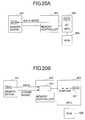
- FIGS. 13A and 13Bare time charts showing relationships between read data, a strobe signal, and a latch signal;
- FIG. 14is a block diagram of a related-art configuration of a latch-signal generation circuit of a memory controller
- FIG. 15is a block diagram of a memory system according to the present invention.
- FIG. 16is a circuit diagram showing the configuration of a variable delay circuit
- FIGS. 17A and 17Bare timing charts for explaining operation of the circuit of FIG. 16;
- FIG. 18is a timing chart for explaining optimum latch timing
- FIG. 19is a flowchart showing a procedure by which a delay is set by a delay selection means comprised of an MPU and a program stored in a ROM;
- FIGS. 20A and 20Bare illustrative drawings for explaining operations for checking correct read timing
- FIG. 21is a timing chart for explaining data read operations during a delay adjustment process
- FIG. 22is a timing chart for explaining data read operations during a delay adjustment process
- FIG. 23is a timing chart for explaining data read operations during a delay adjustment process
- FIG. 24is a timing chart for explaining a data read operation after the completion of delay adjustment.
- FIG. 25is a block diagram of a variable delay circuit used in the present invention.
- FIG. 1is a block diagram of a system to which the present invention is applied.
- the system of FIG. 1includes a memory controller 10 , a memory device 11 , and a microprocessor 12 .
- the memory controller 10acts as an intermediary for control between the microprocessor 12 and the memory device 11 when data read operations and data write operations are performed with respect to the memory device 11 .
- the microprocessor 12 and the memory controller 10exchange data signals, address signals, control signals, and a clock signal.
- the memory controller 10 and the memory device 11exchange strobe signals, data signals, address signals, control signals, and a clock signal.
- the memory controller 10serves to attend to various control operations relating to memory access such as converting bus widths of data buses between the microprocessor 12 and the memory device 11 , carrying out DMA (direct memory access) operations with respect to the memory device 11 , etc.
- the memory device 11operates at a double data rate, and performs the outputting and inputting of data at rising edges and falling edges of a strobe signal.
- the memory controller 10supplies data and a strobe signal to the memory device 11
- the memory device 11supplies data and a strobe signal to the memory controller 10 .
- the strobe signalhas the rising edges and falling edges thereof aligned to the timing of data changes of the data signals.
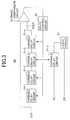
- FIG. 2is a block diagram of an example of the memory controller according to the present invention.
- the memory controller 10 shown in FIG. 2is an example of a memory controller of a particular type that converts data bus widths between the microprocessor 12 and the memory device 11 when the data bus width of the microprocessor 12 is 64 bits and the data bus width of the memory device 11 is 32 bits.
- the memory controller 10 of FIG. 2includes a clock generation circuit 21 , a write control circuit 22 , a read control circuit 23 , an interface 24 , an interface 25 , a delay circuit 26 , a latch circuit 27 , a selector circuit 28 , a selector circuit 29 , and latch circuits 30 through 33 .
- the clock generation circuit 21generates a clock signal CLK, and supplies it to the write control circuit 22 and the read control circuit 23 .
- the clock generation circuit 21further supplies the clock signal CLK to the memory device 11 connected to the memory controller 10 .
- a general configurationis such that a clock signal /CLK inverting the clock signal CLK is supplied in addition to the clock signal CLK.
- the clock generation circuit 21may generate a clock signal CLK 2 having a frequency double the frequency of the clock signal CLK together with a clock signal /CLK 2 that is an inverse thereof.
- 64-bit data supplied from the microprocessor 12is stored in the latch circuits 30 and 31 via the interface 25 , each storing a corresponding 32 bit half.
- the selector circuit 28selects one of the latch circuits 30 and 31 alternately, and supplies the 32 bit data of the selected latch circuit to the memory device 11 via the interface 24 . Operation timing of these operations is controlled by the write control circuit 22 . Further, the write control circuit 22 supplies a data strobe signal to the memory device 11 via the interface 24 .
- 32-bit data read from the memory device 11is supplied to the latch circuit 27 via the interface 24 .
- a strobe signal form the memory device 11is supplied to the delay circuit 26 via the interface 24 .
- the delay circuit 26delays the strobe signal by a 1 ⁇ 4 cycle of the clock signal CLK, and supplies the delayed signal to the latch circuit 27 as a timing signal.
- the latch circuit 27latches the data signals in response to the supplied timing signal.
- the selector circuit 29selects one of the latch circuits 32 and 33 alternately, and supplies the data latched by the latch circuit 27 to the alternately selected latch circuit.
- a total of 64 bits of data collectively stored in the latch circuits 32 and 33are supplied to the microprocessor 12 via the interface 25 .
- the delay circuit 26 and the latch circuit 27together form a data acquisition circuit 50 of the present invention that acquires data signals by delaying the strobe signal by a 1 ⁇ 4 cycle of the clock signal CLK.
- the data acquisition circuit 50receives the clock signal CLK from the clock generation circuit 21 .
- FIG. 3is a block diagram of a first embodiment of the data acquisition circuit 50 according to the present invention.
- the data acquisition circuit 50includes five variable delay circuits 51 - 1 through 51 - 5 , a delay control circuit 52 , a phase comparison circuit 53 , and the latch circuit 27 .
- the variable delay circuits 51 - 1 through 51 - 5have an identical circuit configuration, and are controlled by common control signals supplied from the delay control circuit 52 . As a result, the variable delay circuits 51 - 1 through 51 - 5 always have the same delay.
- the delay circuit 26collectively represents the variable delay circuits 51 - 1 through 51 - 5 , the delay control circuit 52 , and the phase comparison circuit 53 for the sake of clearness of the figure.
- the clock signal CLKis input to one input node of the phase comparison circuit 53 , and is delayed by the four variable delay circuits 51 - 1 through 51 - 4 before being input to the other input node of the phase comparison circuit 53 as a delayed clock signal DCLK.
- the phase comparison circuit 53compares phases between the clock signal CLK and the delayed clock signal DCLK, and supplies results of the phase comparison to the delay control circuit 52 .
- the delay control circuit 52generates control signals for the adjustment of delays of the four variable delay circuits 51 - 1 through 51 - 4 such that the phases of the clock signal CLK and the delayed clock signal DCLK become identical (to be exact, the delayed clock signal DCLK has a phase delayed by 360 degrees). Namely, edge timings are compared between the clock signal CLK and the delayed clock signal DCLK, and the delay is controlled to be increased when the delayed clock signal DCLK has edge timings that are relatively advanced, and is controlled to be decreased when the delayed clock signal DCLK has edge timings that are relatively delayed.
- the delayed clock signal DCLKis controlled to have a 360-degree delay relative to the clock signal CLK. Since the variable delay circuits 51 - 1 through 51 - 4 have an identical circuit configuration and an identical delay, a single variable delay circuit has a delay of a 1 ⁇ 4 cycle of the clock signal CLK when the delayed clock signal DCLK is delayed by 360 degrees behind the clock signal CLK.
- FIG. 4is a timing chart showing relationships between the clock signal CLK, the delayed clock signal DCLK, and the output of the variable delay circuit 51 - 1 .
- the delayed clock signal DCLKis adjusted to be in a 360-degree delay relative to the clock signal CLK.
- the four variable delay circuits 51 - 1 through 51 - 4have the daly thereof equal to one cycle of the clock signal CLK, so that the output of the variable delay circuit 51 - 1 will be delayed from the clock signal CLK by a 1 ⁇ 4 cycle of the clock signal CLK.
- the delay of the variable delay circuit 51 - 1is set equal to the 1 ⁇ 4 cycle of the clock signal CLK.
- variable delay circuit 51 - 5is controlled by the same control signals as the other variable delay circuits so as to have a delay identical to that of other variable delay circuits.
- the variable delay circuit 51 - 5thus has a delay equal to a 1 ⁇ 4 cycle of the clock signal CLK.
- a data strobe signal DS that is input to the variable delay circuit 51 - 5is delayed by the 1 ⁇ 4 cycle of the clock signal CLK, followed by being supplied to the latch circuit 27 as a timing signal.
- the latch circuit 27latches data signals DQ in response to the supplied timing signal.
- the timing signal supplied to the latch circuit 27is obtained by delaying the data strobe signal DS by a 1 ⁇ 4 cycle of the clock signal CLK. Timing of data changes in the data signals DQ corresponds to rising edges and falling edges of the data strobe signal DS.
- the timing signal supplied to the latch circuit 27triggers the latching of the data signals DQ at an exact midpoint between data changes of the data signals DQ. This insures an optimum data-hold time and an optimum data-setup time.
- FIG. 5is a circuit diagram showing an example of a circuit configuration of the delay control circuit 52 and the phase comparison circuit 53 .
- Signals S 1 and S 2 input to the circuit of FIG. 5correspond to the clock signal CLK and the delayed clock signal DCLK, respectively.
- the circuit of FIG. 5includes NAND circuits 141 through 145 , inverters 146 through 149 , NAND circuits 150 and 151 , inverters 152 and 153 , a binary counter 154 , an inverter 155 , NAND circuits 156 and 157 , and inverters 158 and 159 .
- the NAND circuits 141 through 145 and the inverters 146 through 149together form the phase comparison circuit 53 , and the rest of the circuit constitutes the delay control circuit 52 , for example.
- the NAND circuits 144 and 145together form a latch.
- This latchhas two LOW inputs and two HIGH outputs in an initial condition as shown in FIG. 5 .
- the output of the NAND circuit 143becomes HIGH ahead of the output of the NAND circuit 142 .
- the output of the NAND circuit 145thus becomes LOW, while the NAND circuit 144 keeps the HIGH output thereof.
- This conditionis latched by the latch, and, thus, does not change even when the output of the NAND circuit 142 is turned to HIGH by the rising edge of the signal S 2 .
- an output of the inverter 149is HIGH when the signal S 1 has a phase which is ahead in time.
- an output of the inverter 155becomes HIGH.
- a signal from the inverter 148serves to bring the latch to the initial condition at an appropriate timing by simultaneously turning the outputs of the NAND circuits 142 and 143 to LOW. If this configuration was not in place, the outputs of the NAND circuits 143 and 142 would become HIGH successively in this order when the phase of the signal S 1 was ahead in time, and, then, the condition of the latch would be reversed when the signal S 1 became LOW ahead of the signal S 2 , thereby providing a LOW output from the NAND circuit 144 . In order to avoid this, the outputs of the NAND circuits 142 and 143 are changed to LOW at the same time.
- the output of the inverter 148is also provided to the binary counter 154 .
- the binary counter 154has two outputs which become HIGH in turn at every cycle of the input signals S 1 and S 2
- the binary counter 154includes NAND circuits 161 through 168 and inverters 169 through 171 . Operations of the binary counter 154 are well within the scope of ordinary skill in the art, and a description thereof will be omitted.
- the two outputs of the binary counter 154are supplied to one of the two inputs of the NAND circuits 150 and 151 , respectively.
- the other input of the NAND circuits 150 and 151receives the output of the inverter 149 .
- the two outputs of the binary counter 154are supplied to one of the two inputs of the NAND circuits 156 and 157 , respectively.
- the other input of the NAND circuits 156 and 157receives the output of the inverter 155 .
- the inverters 152 and 153which invert outputs of the NAND circuits 150 and 151 , respectively, provide HIGH pulses in turn.
- the inverters 158 and 159which invert outputs of the NAND circuits 156 and 157 , respectively, provide HIGH pulses in turn.
- the HIGH pulses output from the inverters 152 and 153 or the inverters 158 and 159in turn are supplied to the variable delay circuits, thereby adjusting the delays of the variable delay circuits.
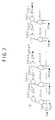
- FIG. 6is a circuit diagram showing a portion of a variable delay circuit.
- FIG. 7is a circuit diagram showing the remaining portion of the variable delay circuit. The circuit configurations of FIG. 6 and FIG. 7 together constitute the entirety of the variable delay circuit.
- the delay-control circuit 135includes NOR circuits 201 - 0 through 201 -n, inverters 202 - 1 through 202 -n, NAND circuits 203 - 1 through 203 -n, NMOS transistors 204 - 1 through 204 -n, NMOS transistors 205 - 1 through 205 -n, NMOS transistors 206 - 1 through 206 -n, and NMOS transistors 207 - 1 through 207 -n.
- a reset signal Ris turned to LOW, the circuit of FIG. 6 is reset.
- an output P( 0 ) of the NOR circuit 201 - 0is HIGH as shown in FIG. 6, and the remaining NOR circuits 201 - 1 through 201 -n have outputs P( 1 ) through P(n), respectively, which are LOW. That is, only the output P( 0 ) is HIGH among the outputs P( 0 ) through P(n)
- HIGH pulsesare supplied to signal lines A and B in turn.
- the NMOS transistor 204 - 1With a HIGH pulse supplied to the signal line B, the NMOS transistor 204 - 1 is turned on. Since the NMOS transistor 206 - 1 is in a turned-on state, an output of the NAND circuit 203 - 1 is connected to the ground, and is forced to change from HIGH to LOW, so that an output of the inverter 202 - 1 becomes HIGH.
- This conditionis latched by the latch comprising the NAND circuit 203 - 1 and the inverter 202 - 1 .
- the output P( 0 )is changed from HIGH to LOW, while the output P( 1 ) is turned from LOW to HIGH. In this condition, therefore, only the output P( 1 ) is HIGH.
- the NMOS transistor 204 - 2With a HIGH pulse supplied to the signal line A, the NMOS transistor 204 - 2 is turned on. Since the NMOS transistor 206 - 2 is already in a turned-on state, an output of the NAND circuit 203 - 2 is connected to the ground, and is forced to change from HIGH to LOW, so that an output of the inverter 202 - 2 becomes HIGH. This condition is latched by the latch comprising the NAND circuit 203 - 2 and the inverter 202 - 2 . As a result, the output P( 1 ) is changed from HIGH to LOW, while the output P( 2 ) is turned from LOW to HIGH. In this condition, therefore, only the output P( 2 ) is HIGH.
- HIGH pulsesare supplied in turn to the signal lines A and B to shift the only one HIGH output among the outputs P( 0 ) through P(n) to the right.
- HIGH pulsesare supplied to signal lines C and D in turn. Operations in this case are simply a reverse of the above-described operations, and a description thereof will be omitted.
- HIGH pulsesare supplied to the signal lines C and D in turn, the only one HIGH output among the outputs P( 0 ) through P(n) will be shifted one by one to the left.
- the output signals P( 1 ) through P(n)are supplied to the circuit portion of the variable delay circuit shown in FIG. 7 so as to adjust a signal delay.
- the circuit portion of the variable delay circuit shown in FIG. 7includes an inverter 210 , NAND circuits 211 - 1 through 211 -n, NAND circuits 212 - 1 through 212 -n, and inverters 213 - 1 through 213 -n.
- the NAND circuits 212 - 1 through 212 -n and the inverters 213 - 1 through 213 -ntogether form a delay line.
- the NAND circuits 211 - 1 through 211 -nhave one input for receiving an inverse of an input signal S 1 from the inverter 210 , and have the other input which is provided with the signals P( 1 ) through P(n), respectively.
- the only one HIGH signal among the signals P( 1 ) through P(n)is denoted as P(x).
- the NAND circuits 211 - 1 through 211 -n, except for the NAND circuit 211 -x,have one input which is LOW, and, thus, have a HIGH output.
- the NAND circuits 212 - 1 through 212 -n, except for the NAND circuit 212 -x,receive this HIGH output at one input thereof, thereby serving as an inverter to the other input thereof.
- a portion of the delay line which is situated upstream from the NAND circuit 212 -xallows a fixed HIGH level to propagate therethrough when this fixed HIGH level is supplied to one input of the NAND circuit 212 -n.
- the NAND circuit 212 -xthus receives the fixed HIGH level at one input thereof.
- the other input of the NAND circuit 212 -xreceives the input signal S 1 via the inverter 210 and the NAND circuit 211 -x.
- Another portion of the delay line from the NAND circuit 212 -x to the inverter 213 - 1allows the input signal S 1 to propagate therethrough with some delays, thereby generating a delayed signal as an output signal SO.
- the output signal SOin this case is delayed by a delay amount commensurate with x stages of delay elements in comparison with the input signal S 1 .
- the phase comparison circuit 53 and the delay control circuit 52 of FIG. 5compare phases of the clock signals, and outputs the pulse signals that alternately become HIGH based on the phase comparison. These pulse signals are supplied to the circuit portion of the variable delay circuit shown in FIG. 6, thereby controlling the position of the only one HIGH signal among the output signals P( 1 ) through P(n).
- the signals P( 1 ) through P(n)set a delay to the circuit portion of the variable delay circuit shown in FIG. 7 .
- FIG. 8is a block diagram showing a second embodiment of the data acquisition circuit according to the present invention.
- a data acquisition circuit 50 Aincludes the three variable delay circuits 51 - 1 , 51 - 2 and 51 - 5 , the delay control circuit 52 , the phase comparison circuit 53 , and the latch circuit 27 .
- An inverted clock signal /CLKwhich is an inverse of the clock signal CLK, is supplied to one input of the phase comparison circuit 53 , and the other input of the phase comparison circuit 53 receives the delayed clock signal DCLK that is the clock signal CLK delayed by the two variable delay circuits 51 - 1 and 51 - 2 .
- the phase comparison circuit 53compares phases between the inverted clock signal /CLK and the delayed clock signal DCLK, and supplies results of the phase comparison to the delay control circuit 52 .
- the delay control circuit 52generates control signals for the adjustment of delays of the two variable delay circuits 51 - 1 and 51 - 2 such that the phases of the inverted clock signal /CLK and the delayed clock signal DCLK become identical. Namely, edge timings are compared between the inverted clock signal /CLK and the delayed clock signal DCLK, and the delay is controlled to be increased when the delayed clock signal DCLK has edge timings that are relatively advanced, and is controlled to be decreased when the delayed clock signal DCLK has edge timings that are relatively delayed.
- the delayed clock signal DCLKis controlled to have the same phase as the inverted clock signal /CLK. That is, the delayed clock signal DCLK is controlled to be placed in a 180-degree phase delay relative to the clock signal CLK. Since the variable delay circuits 51 - 1 and 51 - 2 have an identical circuit configuration and an identical delay, a single variable delay circuit has a delay of a 1 ⁇ 4 cycle of the clock signal CLK when the delayed clock signal DCLK is delayed by 180 degrees from the clock signal CLK.
- the variable delay circuit 51 - 5is controlled by the same control signals as the other variable delay circuits so as to have a delay identical to that of other variable delay circuits.
- the variable delay circuit 51 - 5thus has a delay equal to a 1 ⁇ 4 cycle of the clock signal CLK.
- a data strobe signal DS that is input to the variable delay circuit 51 - 5is delayed by the 1 ⁇ 4 cycle of the clock signal CLK, followed by being supplied to the latch circuit 27 as a timing signal.
- the latch circuit 27latches data signals DQ in response to the supplied timing signal.
- FIG. 9is a block diagram showing a third embodiment of the data acquisition circuit according to the present invention.
- a data acquisition circuit 50 Bincludes the three variable delay circuits 51 - 1 , 51 - 2 and 51 - 5 , the delay control circuit 52 , the phase comparison circuit 53 , and the latch circuit 27 .
- a clock signal CLK 2which has double the frequency of the clock signal CLK, is generated by the clock generation circuit 21 (see FIG. 2 ), and is supplied to one input of the phase comparison circuit 53 .
- the other input of the phase comparison circuit 53receives a delayed clock signal DCLK 2 that is the clock signal CLK 2 delayed by the two variable delay circuits 51 - 1 and 51 - 2 .
- the phase comparison circuit 53compares phases between the clock signal CLK 2 and the delayed clock signal DCLK 2 , and supplies results of the phase comparison to the delay control circuit 52 .
- the delay control circuit 52generates control signals for the adjustment of delays of the two variable delay circuits 51 - 1 and 51 - 2 such that the phases of the clock signal CLK 2 and the delayed clock signal DCLK 2 become identical (to be exact, the delayed clock signal DCLK 2 has a phase delayed by 360 degrees). As a result of this delay adjustment, the delayed clock signal DCLK 2 is controlled to have a 360-degree phase delay relative to the clock signal CLK. Since the variable delay circuits 51 - 1 and 51 - 2 have an identical circuit configuration and an identical delay, a single variable delay circuit has a delay of a 1 ⁇ 2 cycle of the clock signal CLK 2 when the delayed clock signal DCLK 2 is delayed by 360 degrees from the clock signal CLK 2 . When the cycle of the clock signal CLK that is double the cycle of the clock signal CLK 2 is taken into consideration, a single variable delay circuit ends up having a 1 ⁇ 4 cycle delay.
- the variable delay circuit 51 - 5thus has a delay equal to a 1 ⁇ 4 cycle of the clock signal CLK.
- the latch circuit 27latches data signals DQ in response to a timing signal that is delayed by a 1 ⁇ 4 cycle.
- FIG. 10is a block diagram showing a fourth embodiment of the data acquisition circuit according to the present invention.
- a data acquisition circuit 50 C of FIG. 10includes the two variable delay circuits 51 - 1 and 51 - 2 , the delay control circuit 52 , the phase comparison circuit 53 , and the latch circuit 27 .
- a clock signal CLK 2which has double the frequency of the clock signal CLK, is generated by the clock generation circuit 21 (see FIG. 2 ), and an inverted clock signal /CLK 2 that is an inverse thereof is also generated by the clock generation circuit 21 .
- the inverted clock signal /CLK 2is supplied to one input of the phase comparison circuit 53 .
- the other input of the phase comparison circuit 53receives a delayed clock signal DCLK 2 that is the clock signal CLK 2 delayed by the variable delay circuit 51 - 1 .
- the phase comparison circuit 53compares phases between the inverted clock signal /CLK 2 and the delayed clock signal DCLK 2 , and supplies results of the phase comparison to the delay control circuit 52 .
- the delay control circuit 52generates control signals for the adjustment of a delay of the variable delay circuit 51 - 1 such that the phases of the inverted clock signal /CLK 2 and the delayed clock signal DCLK 2 become identical. As a result of this delay adjustment, the delayed clock signal DCLK 2 is controlled to have a 180-degree phase delay relative to the clock signal CLK 2 .
- the variable delay circuit 51 - 1thus has a delay of a 1 ⁇ 2 cycle of the clock signal CLK 2 . When the cycle of the clock signal CLK that is double the cycle of the clock signal CLK 2 is taken into consideration, the variable delay circuit 51 - 1 ends up having a 1 ⁇ 4 cycle delay.
- variable delay circuit 51 - 5has a delay equal to a 1 ⁇ 4 cycle of the clock signal CLK.
- the latch circuit 27latches data signals DQ in response to a timing signal that is delayed by a 1 ⁇ 4 cycle.
- FIG. 11is a block diagram showing a fifth embodiment of the data acquisition circuit according to the present invention.
- the same elements as those of FIG. 3are referred to by the same reference numerals, and a description thereof will be omitted.
- a data acquisition circuit 50 Ddoes not have the delay control circuit 52 compared to the data acquisition circuit 50 of FIG. 3 . Further, the data acquisition circuit 50 D is connected to the microprocessor 12 via the interface 25 (see FIG. 2 ).
- the phase comparison circuit 53 of the data acquisition circuit 50 Dsends the determination of phase comparison to the microprocessor 12 .
- the microprocessor 12supplies control signals so as to control the delay of the variable delay circuits 51 - 1 through 51 - 5 of the data acquisition circuit 50 D.
- the output of the inverter 149 in the phase comparison circuit 53 of FIG. 5may be supplied to the microprocessor 12 via the interface 25 since this output can serve as a signal indicative of which one of the input signals S 1 and S 2 has a rising edge more advanced than the other.
- the microprocessor 12may supply, as control signals, the pulse signals of FIG. 6 that become HIGH alternately to be supplied to either the signal lines A and B or the signal lines C and D depending on whether the delay should be increased or decreased in the variable delay circuit of FIG. 6 .
- phase comparison circuit 53sends the determination of phase comparison (the results of phase comparison) to the microprocessor 12 , and the microprocessor 12 provides the variable delay circuits with control signals for the delay adjustment of variable delay circuits, thereby eliminating a need for circuitry dedicated for delay control purposes. This makes it possible to reduce a circuit size. Since the delay can be adjusted through software control based on programs executed by the microprocessor 12 rather than through hardwired control, it is easier to cope with changes in settings and configurations.
- phase comparison circuit 53sends the determination of phase comparison to the microprocessor, and the control signals for delay adjustment are sent from the microprocessor to the variable delay circuits, is applicable to the second through fourth embodiments of the data acquisition circuit shown in FIG. 8 through FIG. 10 .
- the microprocessor 12can be another microprocessor, a control processor of the similar type, or the like that receives the determination of phase control and supplies control signals for delay control.
- the memory controller 10is of the type that converts data-bus width when the microprocessor 12 has a 64-bit data bus and the memory device 11 has a 32-bit data bus.
- the present inventionis not limited to this particular configuration, but is applicable to various controllers having various control functions.
- a semiconductor integrated circuitreceives signals from an exterior thereof, and carries out operations responsive to the input signals, followed by outputting output signals. It is thus important what timing the output signals are obtained relative to the timing of the input signals.
- timingis generally defined in the specification.
- DRAMsdynamic random access memories
- various requirementsare defined with respect to a maximum frequency of the address signals, timing of data outputs relative to the edges of address signals, a data-setup time for writing data, etc.
- SDRAMssynchronous DRAMs
- SDRAMsattend to data input/output operation in synchronization with a high-speed clock signal supplied from an external source.
- Internal operationsare pipelined typically, with the operations of pipelines being performed in parallel, thereby achieving a fast operation speed.
- datais input and output in synchronization with both the falling edges and the rising edges of the clock signal.
- DDRdouble-data-rate
- a latch circuitWhen data is read from or written to a memory device, a latch circuit is used to latch data. Such latching operation needs to be carried out when data is stable. In high-speed memory devices, an interval between successive data inputs/outputs is very short, so that the latch timing needs to be accurately defined relative to the data timing in order to latch the data that is stable.
- dataOn the data output side, data is output in synchronization with a strobe signal, which is also output.
- the strobe signalis similar to clock signal in that it has a predetermined cycle, and is generally generated from a clock signal.
- the strobe signalOn the data input side, the strobe signal is delayed to generate a latch signal, which is used to latch the data at an optimum timing.
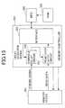
- FIG. 12is a block diagram of a memory system using s synchronous memory device.
- a microprocessor (MPU) 303is connected to a synchronous memory device 301 via a memory controller 302 .
- a clock source 304supplies a system clock signal CK to the MPU 303 , and also supplies the system clock signal CK to the memory controller 302 .
- An interface 325 of the memory controller 302receives data to be written and address signals from the MPU 303 , and supplies data read from the memory device to the MPU 303 . Further, The interface 325 generates a clock signal CLK from the system clock signal CK, and supplies the clock signal CLK to a write-data-output-timing adjustment circuit 321 . The clock signal CLK is also supplied from the memory controller 302 to the memory device 301 .
- a write-data-output circuit 322outputs the data to be written in synchronization with an output timing signal that is supplied from the write-data-output-timing adjustment circuit 321 .
- the write-data-output-timing adjustment circuit 321adjusts the timing of the output timing signal such that the data to be written changes at the edge timing of the clock signal CLK, for example.
- a latch-signal generation circuit 311 of the memory device 301delays the clock signal CLK to generate a latch signal, which is supplied to a write-data-latch circuit 312 .
- the write-data-output circuit 322 of the memory controller 302changes the write data in synchronization with the edges of the clock signal CLK, so that the latch-signal generation circuit 311 generates the latch signal by delaying the clock signal CLK by half the cycle for an ordinary data rate configuration, and generates complementary latch signals by delaying the clock signal CLK by a 1 ⁇ 4 cycle for a double data rate configuration.
- the write data latched by the write-data-latch circuit 312is supplied to and stored in an internal circuit 315 .
- the clock signal CLKserves as a strobe signal for the transmission of write data.
- Address signals and control signalsare supplied from the memory controller 302 to the memory device 301 in the same manner.
- the memory controller 302is thus provided with output circuits for outputting the address signals and control signals, and the memory device 301 is provided with input circuits for inputting these signals.
- these circuitsare omitted from FIG. 12, and will be omitted in descriptions that follow.
- the internal circuit 315supplies the data to a data-output circuit 313 .
- An output-timing adjustment circuit 314delays the clock signal CLK to generate a strobe signal.
- the data-output circuit 313outputs the data in synchronization with an output timing signal supplied from the output-timing adjustment circuit 314 .
- the output-timing adjustment circuit 314adjusts the timing of the output timing signal such that the output data changes in synchronization with the edges of the strobe signal, for example.
- a latch-signal generation circuit 324 of the memory controller 302delays the strobe signal to generate a latch signal, and supplies the latch signal to a read-data latch circuit 323 .
- the read-data latch circuit 323latches the read data in response to the latch signal.
- the data-output circuit 313 of the memory device 301changes the output read data in synchronization with the edges of the strobe signal, so that the latch-signal generation circuit 324 generates the latch signal by delaying the strobe signal by half the cycle for the ordinary data rate configuration, and generates complementary latch signals by delaying the strobe signal by a 1 ⁇ 4 cycle for the double data rate configuration.
- the read data latched by the read-data latch circuit 323is supplied to the MPU 303 via the interface 325 .
- the data to be writtenis output in synchronization with the clock signal. Since the crucial issues to be addressed for achieving high-speed memory devices are the issues of data read speed, and the data write operation can be actually carried out at slower speed, the data to be written may be output without any synchronization with a clock signal. Moreover, if the clock signal is regarded as a strobe signal, then, the data write operation and the data read operation are substantially the same in terms of the transmission and reception of data. In the following, only a description of transmission and reception of read data will be given without referring to transmission and reception of write data.
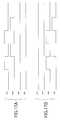
- FIGS. 13A and 13Bare time charts showing relationships between the read data, the strobe signal, and the latch signal.
- FIG. 13Ashows the case of the ordinary data rate
- FIG. 13Bshows the case of the double data rate.
- the strobe signalhas a cycle identical to that of the clock signal.
- the latch signalmay be preferably designed to have rising edges at midpoint between changes of the output data DQ, so that the latch-signal generation circuit 324 delays the strobe signal by half a cycle.
- the double data rateas shown in FIG.
- the read data DQchanges at both the rising edges and the falling edges of the strobe signal. Accordingly, the latch-signal generation circuit 324 delays the strobe signal by a 1 ⁇ 4 cycle to generate a latch signal a, and also generates a latch signal b that is complementary to the latch signal a (i.e., the latch signal b is delayed from the strobe signal by a 3 ⁇ 4 cycle).
- FIG. 14is a block diagram of a related-art configuration of the latch-signal generation circuit of the memory controller 302 .
- a delay line 241is provided to delay the strobe signal by a delay length as described above.
- the delay line 241includes inverters connected in series, and a delay can be adjusted by selecting the position at which an output is taken out of the delay line 241 . By taking into account the clock cycle and delays of various portions in the memory system, the delay of the delay line 241 is determined.
- the delay of the delay line 241is selectable, a delay that is once selected will be fixed. Further, the delay needs to be determined by taking into account the clock cycle and the delays of various portions with respect to each specific memory system, which requires excessive time and labor. Moreover, if the delay of the delay line 241 or the delays of various portions change due to temperature changes, power-supply-voltage fluctuation, etc., the latch signal may be deviated from the optimum latch timing.
- the latch-signal generation circuit 311 of the memory device 301 shown in FIG. 12needs a delay circuit similar to the one described above.
- the delay line 241 of FIG. 14may be used in the latch-signal generation circuit 311 .
- the delayis fixed, which gives rise to a need that use of the memory device is limited to use with a particular clock frequency. This thus sacrifices universal applicability of the device.
- Japanese Patent Laid-open Application No. 10-228449teaches a memory device having a latch-signal generation circuit, which includes a variable delay line having a variable delay and a dummy delay line that is equivalent to the variable delay line, wherein feedback control is carried out to achieve an optimum latch timing by comparing the phase of a clock signal with the phase of a dummy signal delayed by the dummy delay line.
- Japanese Patent Laid-open Application No. 10-228449further teaches providing a plurality of variable delay lines where one variable delay line receives an output of another variable delay line provided at a preceding stage, and each variable delay line is commonly controlled with respect to the delay thereof.
- phase controlis attended to so as to make the output of the variable delay lines have the same phase as the clock signal, thereby generating a signal having a predetermined phase shift. If the configuration disclosed in the Japanese Patent Laid-open Application No. 10-228449 is applied to the latch-signal generation circuit of the memory controller, it is possible to generate a latch signal that is applicable to any memory system of any configuration, and that is optimum at all times even if there is temperature variation.
- the configuration disclosed in the Japanese Patent Laid-open Application No. 10-228449includes a plurality of variable delay lines, which is undesirable in that the circuit becomes complex and large. Further, a plurality of variable delay lines arranged in series has a minimum adjustable delay length that is a multiple of the delay of one delay stage of each variable delay line. If four variable delay lines are provided in series, four signals are generated that have respective phases staggered by a 1 ⁇ 4 cycle each. In this case, however, the minimum adjustable delay length is four times as long, so that precise adjustment cannot be made. Further, if the delay of one delay stage in each variable delay line is made shorter, the number of delay stages needs to be increased, resulting in a circuit-size increase.
- the configuration as shown in FIG. 3 which uses a delay line for delay settingoffers only a fixed delay, and the delay setting needs to be made with respect to each specific memory system, which is laborious and time consuming, and, also, gives rise to a problem that the latch signal deviates from an optimum latch timing when the delay varies due to manufacturing process variation, temperature variation, power-supply-voltage variation, etc.
- the configuration disclosed in the Japanese Patent Laid-open Application No. 10-228449has a drawback in that the circuit becomes complex and large.
- FIG. 15is a block diagram of a memory system according to the present invention.
- the microprocessor (MPU) 303is connected to the memory controller 302 , which is connected to the double-data-rate (DDR) memory device 301 .
- the MPU 303accesses the DDR memory device 301 via the memory controller 302 .
- the MPU 303has a ROM 305 connected thereto where the ROM 305 stores a read-operation control program therein.
- the MPU 303When the MFU 303 is to write date in the DDR memory device 301 , the MPU 303 supplies control signals, address signals, and the write data to the interface 325 of the memory controller 302 .
- the memory controller 302generates control signals and address signals for the DDR memory device 301 based on the received control signals and the received address signals, and supplies the generated control signals and address signals together with the write data to the DDR memory device 301 .
- the MPU 303When the MPU 303 is to read data from the DDR memory device 301 , the MPU 303 supplies control signals and address signals to the interface 325 of the memory controller 302 .
- the memory controller 302then generates control signals and address signals for the DDR memory device 301 based on the received control signals and the received address signals, and supplies the generated control signals and address signals to the DDR memory device 301 .
- the DDR memory device 301outputs data such that the data exhibits changes in synchronization with both the rising edges and the falling edges of the strobe signal as shown in FIG. 13B, and, also, the strobe signal is output together with the data.
- a variable delay circuit 242 of the memory controller 302delays a strobe signal to generate a latch signal.
- the latch circuit 323latches the read data in response to the latch signal.
- the latched datais read by the MPU 303 via the interface 325 .
- the variable delay circuit 242is configured to allow a delay thereof to be selected by a delay selection signal that is input via the interface 325 from the MPU 303 .
- the ROM 305stores therein a program for setting the delay selection signal, which is supplied to the variable delay circuit 242 .
- This programis executed at the time of power-on of the memory system and at constant intervals thereafter.
- the MPU 303 and the program stored in the ROM 305together form a means to select a delay (i.e., the delay selection means or the delay selection unit).
- This means to select a delaymay as well be implemented by hardware circuitry.
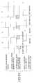
- FIG. 16is a circuit diagram showing the configuration of the variable delay circuit 242 .
- the variable delay circuitdelays a signal IN (strobe signal) that passes through two inverters 361 and 362 , thereby producing a signal OUT.
- the delayis adjusted by changing capacitance coupled to the signal line that connects between the two inverters 361 and 362 .
- the signal line that connects between the two inverters 361 and 362has a plurality of sets of registers R and transistors TR connected thereto where each set is comprised of one register R and one transistor TR connected in series. As the number of transistors that are made conductive changes, the capacitance coupled to the signal line also changes.
- a circuit portion indicated by reference number 363is a shift register. As the reset signal RST becomes HIGH, flip-flops each constituting a register of a corresponding stage are all placed in the same conditions, in which the an output of each register applied to the gate of the transistor TR is set equal to LOW, thereby making all the transistors TR nonconductive.
- FIGS. 17A and 17Bare timing charts showing operation of the circuit of FIG. 16 .
- a control signalare generated from the delay selection signal is set equal to HIGH (all other control signals sro, sle, and slo remain LOW)
- the output of the first registerbecomes HIGH, thereby making the transistor TR conductive at the first stage. Since the other transistors TR remain nonconductive, the overall capacitance changes by one stage's worth of capacitance, resulting in a slight increase in the delay of the output signal OUT.
- the control signal srois changed to HIGH, the output of the second register is also changed to HIGH, thereby making the second-stage transistor TR conductive.
- the overall capacitanceends up having two stages' worth of capacitance increases, thereby delaying the output signal OUT slightly more.
- the control signals sre and sroare alternately changed to HIGH so as to make the transistors TR conductive one after another from left to to the right, thereby successively increasing the capacitance coupled to the signal line to increase the delay of the output signal OUT.
- the variable delay circuit of FIG. 16delays the input signal (strobe signal) IN by a delay specified by the delay selection signal, thereby producing the output signal OUT.
- FIG. 18is a timing chart for explaining optimum latch timing.
- the latch circuitlatches data at a rising edge of the latch signal.
- a time period during which the data needs to be stable before the rising edgeis referred to as a setup time
- a time period during which the data needs to be stable after the rising edgeis referred to as a hold time.
- the memory device of this embodimentis that of a DDR type, data changes at rising edges and falling edges of the strobe signal.
- the memory device 301includes an output timing adjustment circuit for controlling the data to change exactly at the rising edges and falling edges of the strobe signal.
- the data and the strobe signalare displaced from each other to some extent because of a circuit variation, a time difference in signal propagation from the DDR memory device 301 to the memory controller 302 , etc.
- a time period during which data acquisition is reliably performedis actually shorter than a time period between the two edges, and is referred to as a data-valid period.
- a range during which a valid latch operation is possibleends up being a range as shown by hatching in FIG. 18 .
- the latch signalis adjusted so as to rise at the midpoint of this hatched range.
- FIG. 19is a flowchart showing a procedure by which a delay is set by the delay selection means comprised of the MPU 303 and the program stored in the ROM 305 .
- FIGS. 20A and 20Bare illustrative drawings for explaining operations for checking correct read timing.
- FIGS. 21 through 24are timing charts for explaining data read operations during an adjustment process and after the completion of adjustment. In the following, the procedure for setting a delay will be described with reference to these drawings.
- the reset signal RSTis input to the variable delay circuit 242 of FIG. 16, so that the delay of the variable delay circuit 242 is set to the minimum setting thereof.
- the MPU 303reads reference data from the ROM 305 , and writes the data in the memory device 301 via the memory controller 302 . Also, the data is stored in a register 331 of the MPU 303 . In this example, the reference data is “0010”.
- the MPU 303reads the reference data that has just been stored from the memory device 301 via the memory controller 302 . That is, the memory device 301 outputs the reference data in synchronization with the strobe signal, and the latch circuit 323 of the memory controller 302 latches the reference data in response to the latch signal supplied from the variable delay circuit 242 . The reference data that is latched is then supplied to the MFU 303 .
- the MPU 303compares the obtained reference data with the reference data stored in the register 331 , and checks whether they match.
- the delay of the variable delay circuit 242was set to the minimum setting thereof at step 101 , so that the latch signal is slightly delayed behind the strobe signal as shown in FIG. 21 .
- step 105the delay of the variable delay circuit 242 is increased by one stage in response to the delay selection signal.
- the control signal sre or sro shown in FIG. 16is changed to HIGH. Thereafter, the procedure goes back to step 103 , and the operations from step 103 to step 105 will be repeated.
- the delay of the variable delay circuit 242is increased, eventually resulting in the latch signal being adjusted to change after the passage of the setup time following data changes.
- the obtained reference datais “0010” as shown in FIG. 22, and is identified at step 104 as matching the correct reference data stored in the register
- the procedure in this casegoes to step 106 , at which the current delay is stored as a delay t 1 .
- the reference datais read from the memory device 301 in the same manner as was read at step 103 .
- a checkis made as to whether the obtained reference data fails to match the reference data stored in the register 331 . If they match, the procedure goes to step 109 , at which the delay of the variable delay circuit 242 is increased by one stage. Thereafter, the procedure goes back to step 107 , and the operations of steps 107 through 109 will be repeated.
- the delay of the variable delay circuit 242is increased, eventually resulting in the latch signal being adjusted such as to have a data change less the hold time after the latch signal change.
- the obtained reference datais “0100” as shown in FIG. 23, and is identified at step 108 as failing to match the correct reference data stored in the register.
- the procedure in this casegoes to step 110 , at which the current delay is stored as a delay t 2 .
- the delays t 1 and t 2demarcate a range of the delay of the variable delay circuit 242 within which proper read operation is performed.
- a delay t 3is obtained as:
- the delay of the variable delay circuit 242is decreased exactly by the delay t 3 .
- the latch signalmaintains relationship with the data as shown in FIG. 24, in which the delay is positioned at the midpoint of the range that extends from the delay t 1 to the delay t 2 . This puts an end to the delay setting procedure.
- the adjusted delayis kept as it is.
- the program for setting the delay selection signal stored in the ROM 305is activated at constant intervals, the delay adjusted at every turn will be maintained until the next following delay setting operation.
- variable delay circuitas shown in FIG. 25 and as disclosed in Japanese Patent Laid-open Application No. 10-228449 may be employed.
- This variable delay circuitincludes a delay line comprised of a plurality of delay elements 372 connected in series and a selector 373 that selects one of the outputs of the delay elements 372 .
- the variable delay circuitincludes a shift register 374 that indicates the point where the output is selected by the selector 373 , thereby adjusting the delay by changing the number of relevant delay elements 372 in response to the position of selection. It should be noted that such a variable delay circuit may be implemented by using the circuit structures shown in FIG. 6 and FIG. 7 .
- the present inventioncan implement a memory system having a simple structure that can latch data at optimum timing as the data is read from a memory device, and can also set the latch timing to the optimum timing even if there is manufacturing variation, temperature variation, power-supply-voltage variation, etc.
- the present inventioncan thus achieve a memory system at low costs that is capable of high speed data read operations.
Landscapes
- Engineering & Computer Science (AREA)
- Theoretical Computer Science (AREA)
- Physics & Mathematics (AREA)
- General Engineering & Computer Science (AREA)
- General Physics & Mathematics (AREA)
- Dram (AREA)
Abstract
Description
Claims (20)
Applications Claiming Priority (4)
| Application Number | Priority Date | Filing Date | Title |
|---|---|---|---|
| JP2000148480AJP4778132B2 (en) | 2000-05-19 | 2000-05-19 | Memory controller and system |
| JP2000-148480 | 2000-05-19 | ||
| JP2000158336AJP2001337862A (en) | 2000-05-29 | 2000-05-29 | Memory system and its setup method |
| JP2000-158336 | 2000-05-29 |
Publications (2)
| Publication Number | Publication Date |
|---|---|
| US20010046163A1 US20010046163A1 (en) | 2001-11-29 |
| US6466491B2true US6466491B2 (en) | 2002-10-15 |
Family
ID=26592242
Family Applications (1)
| Application Number | Title | Priority Date | Filing Date |
|---|---|---|---|
| US09/859,489Expired - LifetimeUS6466491B2 (en) | 2000-05-19 | 2001-05-18 | Memory system and memory controller with reliable data latch operation |
Country Status (1)
| Country | Link |
|---|---|
| US (1) | US6466491B2 (en) |
Cited By (38)
| Publication number | Priority date | Publication date | Assignee | Title |
|---|---|---|---|---|
| US6603686B2 (en)* | 2001-03-09 | 2003-08-05 | Samsung Electronics Co., Ltd. | Semiconductor memory device having different data rates in read operation and write operation |
| US6618457B1 (en)* | 1998-12-22 | 2003-09-09 | Hyundai Electronics Industries Co., Ltd. | Apparatus and method for receiving external data signal to generate internal data signal |
| US20030223278A1 (en)* | 2002-05-30 | 2003-12-04 | Gomm Tyler J. | Dynamically centered setup-time and hold-time window |
| US20040260962A1 (en)* | 2003-06-23 | 2004-12-23 | Victor Suen | Systems and methods for latching data |
| US20050007836A1 (en)* | 2003-07-09 | 2005-01-13 | Morzano Christopher K. | Data strobe synchronization circuit and method for double data rate, multi-bit writes |
| US20050041487A1 (en)* | 2002-04-02 | 2005-02-24 | Via Technologeis, Inc. | Method and system for writing data to a memory |
| US20050047222A1 (en)* | 2003-08-27 | 2005-03-03 | Rentschler Eric Mccutcheon | Data signal reception latch control using clock aligned relative to strobe signal |
| US6889334B1 (en)* | 2001-10-02 | 2005-05-03 | Advanced Micro Devices, Inc. | Multimode system for calibrating a data strobe delay for a memory read operation |
| US20060052961A1 (en)* | 2004-08-20 | 2006-03-09 | Best Scott C | Individual data line strobe-offset control in memory systems |
| US20060120208A1 (en)* | 2004-08-31 | 2006-06-08 | Kim Kang Y | Delay-locked loop having a pre-shift phase detector |
| US20060120193A1 (en)* | 2004-12-03 | 2006-06-08 | Casper Stephen L | System and method for reducing power consumption during extended refresh periods of dynamic random access memory devices |
| US20060136769A1 (en)* | 2004-12-21 | 2006-06-22 | Kizer Jade M | Interface circuit for strobe-based systems |
| US20060203577A1 (en)* | 2004-04-30 | 2006-09-14 | Hyun Woo Lee | Data output controller in semiconductor memory device and control method thereof |
| US20060203602A1 (en)* | 2005-03-14 | 2006-09-14 | Rambus, Inc. | Self-timed interface for strobe-based systems |
| US7123051B1 (en) | 2004-06-21 | 2006-10-17 | Altera Corporation | Soft core control of dedicated memory interface hardware in a programmable logic device |
| US7126399B1 (en) | 2004-05-27 | 2006-10-24 | Altera Corporation | Memory interface phase-shift circuitry to support multiple frequency ranges |
| US7167023B1 (en) | 2001-08-29 | 2007-01-23 | Altera Corporation | Multiple data rate interface architecture |
| US20070104015A1 (en)* | 2005-11-10 | 2007-05-10 | Vaishnav Srinivas | Clock signal generation techniques for memories that do not generate a strobe |
| US7231536B1 (en) | 2001-08-29 | 2007-06-12 | Altera Corporation | Control circuit for self-compensating delay chain for multiple-data-rate interfaces |
| US7234069B1 (en) | 2004-03-12 | 2007-06-19 | Altera Corporation | Precise phase shifting using a DLL controlled, multi-stage delay chain |
| US20070201279A1 (en)* | 2001-12-19 | 2007-08-30 | Hiroshi Nakamura | Semiconductor integrated circuit adapted to output pass/fail results of internal operations |
| US20070217559A1 (en)* | 2006-03-16 | 2007-09-20 | Rambus Inc. | Signaling system with adaptive timing calibration |
| US20070237010A1 (en)* | 2002-04-02 | 2007-10-11 | Via Technologies, Inc. | Method and system for reading data from a memory |
| US20070291830A1 (en)* | 2006-05-26 | 2007-12-20 | Nec Electronics Corporation | Interface circuit and memory controller |
| US20080089147A1 (en)* | 2006-10-17 | 2008-04-17 | Hynix Semiconductor Inc. | Circuit and method for generating column path control signals in semiconductor device |
| US20080101138A1 (en)* | 2006-10-31 | 2008-05-01 | Samsung Electronics Co., Ltd. | Methods of operating non-volatile memory devices to generate data strobe signals during data reading and related devices |
| KR100835626B1 (en) | 2005-09-16 | 2008-06-09 | 후지쯔 가부시끼가이샤 | Timing adjustment circuit, LSI and data transmission / reception system of data transmission / reception circuit |
| US7512193B1 (en)* | 2005-05-02 | 2009-03-31 | National Semiconductor Corporation | Circuit and method for pre-emphasis in data serialization |
| US20090238017A1 (en)* | 2006-12-05 | 2009-09-24 | Fujitsu Microelectronics Limited | Digital dll circuit |
| US20100315892A1 (en)* | 2004-12-28 | 2010-12-16 | Panasonic Corporation | Method and apparatus for timing adjustment |
| US7924049B1 (en)* | 2007-12-19 | 2011-04-12 | Altera Corporation | Accelerated programming technique for integrated circuits |
| US20110267117A1 (en)* | 2010-04-28 | 2011-11-03 | Hae-Rang Choi | Data input/output apparatus and method for semiconductor system |
| US20150058705A1 (en)* | 2013-08-23 | 2015-02-26 | Kabushiki Kaisha Toshiba | Storage device and data latch timing adjustment method |
| US20150262647A1 (en)* | 2011-09-16 | 2015-09-17 | Ps4 Luxco S.A.R.L. | Semiconductor Device Latching Data Signal In Response To Strobe Signal And Information Processing System Including The Same |
| CN105706172A (en)* | 2013-12-06 | 2016-06-22 | 英特尔公司 | Method for training a control signal based on a strobe signal in a memory module |
| USRE46819E1 (en)* | 2006-06-30 | 2018-05-01 | Conversant Intellectual Property Management Inc. | Synchronous memory read data capture |
| US20190355410A1 (en)* | 2018-05-08 | 2019-11-21 | Micron Technology, Inc. | Half-Width, Double Pumped Data Path |
| US20240257850A1 (en)* | 2023-02-01 | 2024-08-01 | Samsung Electronics Co., Ltd. | Memory system, operating method of the memory system, and interface circuit of the memory system |
Families Citing this family (60)
| Publication number | Priority date | Publication date | Assignee | Title |
|---|---|---|---|---|
| US6678811B2 (en)* | 2001-04-07 | 2004-01-13 | Hewlett-Packard Development Company, L.P. | Memory controller with 1X/MX write capability |
| US6633965B2 (en) | 2001-04-07 | 2003-10-14 | Eric M. Rentschler | Memory controller with 1×/M× read capability |
| US6889335B2 (en)* | 2001-04-07 | 2005-05-03 | Hewlett-Packard Development Company, L.P. | Memory controller receiver circuitry with tri-state noise immunity |
| US6625702B2 (en)* | 2001-04-07 | 2003-09-23 | Hewlett-Packard Development Company, L.P. | Memory controller with support for memory modules comprised of non-homogeneous data width RAM devices |
| US7000065B2 (en)* | 2002-01-02 | 2006-02-14 | Intel Corporation | Method and apparatus for reducing power consumption in a memory bus interface by selectively disabling and enabling sense amplifiers |
| US7050507B2 (en)* | 2002-04-22 | 2006-05-23 | Intel Corporation | Adaptive throughput pulse width modulation communication scheme |
| JP4136577B2 (en)* | 2002-09-30 | 2008-08-20 | Necエレクトロニクス株式会社 | Memory control device and data processing device |
| US7076677B2 (en)* | 2002-12-30 | 2006-07-11 | Intel Corporation | Same edge strobing for source synchronous bus systems |
| US6791889B2 (en)* | 2003-02-04 | 2004-09-14 | Intel Corporation | Double data rate memory interface |
| US20050050375A1 (en)* | 2003-08-29 | 2005-03-03 | Mark Novak | Memory interface system and method |
| US7259606B2 (en) | 2004-01-27 | 2007-08-21 | Nvidia Corporation | Data sampling clock edge placement training for high speed GPU-memory interface |
| US7290160B2 (en)* | 2004-11-23 | 2007-10-30 | Intel Corporation | Method and apparatus to deskew data to clock for memory |
| US7493461B1 (en) | 2005-01-20 | 2009-02-17 | Altera Corporation | Dynamic phase alignment for resynchronization of captured data |
| US8386722B1 (en) | 2008-06-23 | 2013-02-26 | Google Inc. | Stacked DIMM memory interface |
| US9542352B2 (en) | 2006-02-09 | 2017-01-10 | Google Inc. | System and method for reducing command scheduling constraints of memory circuits |
| US8090897B2 (en) | 2006-07-31 | 2012-01-03 | Google Inc. | System and method for simulating an aspect of a memory circuit |
| US8041881B2 (en) | 2006-07-31 | 2011-10-18 | Google Inc. | Memory device with emulated characteristics |
| US8077535B2 (en) | 2006-07-31 | 2011-12-13 | Google Inc. | Memory refresh apparatus and method |
| US8438328B2 (en) | 2008-02-21 | 2013-05-07 | Google Inc. | Emulation of abstracted DIMMs using abstracted DRAMs |
| US8111566B1 (en) | 2007-11-16 | 2012-02-07 | Google, Inc. | Optimal channel design for memory devices for providing a high-speed memory interface |
| US8089795B2 (en) | 2006-02-09 | 2012-01-03 | Google Inc. | Memory module with memory stack and interface with enhanced capabilities |
| US8130560B1 (en) | 2006-11-13 | 2012-03-06 | Google Inc. | Multi-rank partial width memory modules |
| US10013371B2 (en) | 2005-06-24 | 2018-07-03 | Google Llc | Configurable memory circuit system and method |
| US9507739B2 (en) | 2005-06-24 | 2016-11-29 | Google Inc. | Configurable memory circuit system and method |
| US8359187B2 (en) | 2005-06-24 | 2013-01-22 | Google Inc. | Simulating a different number of memory circuit devices |
| US20080082763A1 (en) | 2006-10-02 | 2008-04-03 | Metaram, Inc. | Apparatus and method for power management of memory circuits by a system or component thereof |
| US9171585B2 (en) | 2005-06-24 | 2015-10-27 | Google Inc. | Configurable memory circuit system and method |
| US20080028136A1 (en) | 2006-07-31 | 2008-01-31 | Schakel Keith R | Method and apparatus for refresh management of memory modules |
| US8796830B1 (en) | 2006-09-01 | 2014-08-05 | Google Inc. | Stackable low-profile lead frame package |
| US8327104B2 (en)* | 2006-07-31 | 2012-12-04 | Google Inc. | Adjusting the timing of signals associated with a memory system |
| US7386656B2 (en) | 2006-07-31 | 2008-06-10 | Metaram, Inc. | Interface circuit system and method for performing power management operations in conjunction with only a portion of a memory circuit |
| US8397013B1 (en) | 2006-10-05 | 2013-03-12 | Google Inc. | Hybrid memory module |
| US8055833B2 (en) | 2006-10-05 | 2011-11-08 | Google Inc. | System and method for increasing capacity, performance, and flexibility of flash storage |
| US7609567B2 (en) | 2005-06-24 | 2009-10-27 | Metaram, Inc. | System and method for simulating an aspect of a memory circuit |
| US8081474B1 (en) | 2007-12-18 | 2011-12-20 | Google Inc. | Embossed heat spreader |
| US8244971B2 (en) | 2006-07-31 | 2012-08-14 | Google Inc. | Memory circuit system and method |
| US8335894B1 (en) | 2008-07-25 | 2012-12-18 | Google Inc. | Configurable memory system with interface circuit |
| US8060774B2 (en) | 2005-06-24 | 2011-11-15 | Google Inc. | Memory systems and memory modules |
| KR101377305B1 (en) | 2005-06-24 | 2014-03-25 | 구글 인코포레이티드 | An integrated memory core and memory interface circuit |
| WO2007028109A2 (en) | 2005-09-02 | 2007-03-08 | Metaram, Inc. | Methods and apparatus of stacking drams |
| US9632929B2 (en) | 2006-02-09 | 2017-04-25 | Google Inc. | Translating an address associated with a command communicated between a system and memory circuits |
| WO2007127678A2 (en)* | 2006-04-24 | 2007-11-08 | Sandisk Corporation | High-performance flash memory data transfer |
| US7647467B1 (en) | 2006-05-25 | 2010-01-12 | Nvidia Corporation | Tuning DRAM I/O parameters on the fly |
| US7882322B2 (en)* | 2006-06-27 | 2011-02-01 | International Business Machines Corporation | Early directory access of a double data rate elastic interface |
| US7734944B2 (en)* | 2006-06-27 | 2010-06-08 | International Business Machines Corporation | Mechanism for windaging of a double rate driver |
| US7783911B2 (en)* | 2006-06-27 | 2010-08-24 | International Business Machines Corporation | Programmable bus driver launch delay/cycle delay to reduce elastic interface elasticity requirements |
| US7752475B2 (en)* | 2006-06-27 | 2010-07-06 | International Business Machines Corporation | Late data launch for a double data rate elastic interface |
| US7739538B2 (en)* | 2006-06-27 | 2010-06-15 | International Business Machines Corporation | Double data rate chaining for synchronous DDR interfaces |
| US7724589B2 (en) | 2006-07-31 | 2010-05-25 | Google Inc. | System and method for delaying a signal communicated from a system to at least one of a plurality of memory circuits |
| US7928770B1 (en)* | 2006-11-06 | 2011-04-19 | Altera Corporation | I/O block for high performance memory interfaces |
| WO2008079910A2 (en)* | 2006-12-20 | 2008-07-03 | Rambus Inc. | Strobe acquisition and tracking |
| KR100895072B1 (en)* | 2007-03-08 | 2009-04-27 | 삼성전자주식회사 | Memory system that can guarantee the stability of read data and its data reading method |
| US8209479B2 (en) | 2007-07-18 | 2012-06-26 | Google Inc. | Memory circuit system and method |
| US8080874B1 (en) | 2007-09-14 | 2011-12-20 | Google Inc. | Providing additional space between an integrated circuit and a circuit board for positioning a component therebetween |
| US8121239B2 (en)* | 2008-02-11 | 2012-02-21 | Intel Corporation | Unidirectional sweep training for an interconnect |
| DE202010017690U1 (en) | 2009-06-09 | 2012-05-29 | Google, Inc. | Programming dimming terminating resistor values |
| WO2011156041A1 (en)* | 2010-06-08 | 2011-12-15 | Rambus Inc. | Integrated circuit device timing calibration |
| KR102112024B1 (en) | 2014-04-14 | 2020-05-19 | 삼성전자주식회사 | Method for forming strobe signal in data storage system and therefore device |
| KR102736271B1 (en)* | 2016-09-09 | 2024-12-02 | 삼성전자주식회사 | Memory System and Memory Control Method |
| US11115006B1 (en)* | 2020-10-23 | 2021-09-07 | Integrated Silicon Solution Inc. | Internal latch circuit and method for generating latch signal thereof |
Citations (3)
| Publication number | Priority date | Publication date | Assignee | Title |
|---|---|---|---|---|
| JPS5538604A (en)* | 1978-09-04 | 1980-03-18 | Nippon Telegr & Teleph Corp <Ntt> | Memory device |
| US5537602A (en)* | 1988-09-16 | 1996-07-16 | Hitachi, Ltd. | Process system for controlling bus system to communicate data between resource and processor |
| JPH10228449A (en) | 1996-09-17 | 1998-08-25 | Fujitsu Ltd | Semiconductor device system and semiconductor device |
- 2001
- 2001-05-18USUS09/859,489patent/US6466491B2/ennot_activeExpired - Lifetime
Patent Citations (4)
| Publication number | Priority date | Publication date | Assignee | Title |
|---|---|---|---|---|
| JPS5538604A (en)* | 1978-09-04 | 1980-03-18 | Nippon Telegr & Teleph Corp <Ntt> | Memory device |
| US5537602A (en)* | 1988-09-16 | 1996-07-16 | Hitachi, Ltd. | Process system for controlling bus system to communicate data between resource and processor |
| JPH10228449A (en) | 1996-09-17 | 1998-08-25 | Fujitsu Ltd | Semiconductor device system and semiconductor device |
| US6028816A (en) | 1996-09-17 | 2000-02-22 | Fujitsu Limited | System configured of synchronous semiconductor device for adjusting timing of each input and semiconductor device used therefor |
Non-Patent Citations (1)
| Title |
|---|
| Betty Prince, "Semiconductor Memories", 1983, Wiley, 2nd edition, pp. 470-472.* |
Cited By (122)
| Publication number | Priority date | Publication date | Assignee | Title |
|---|---|---|---|---|
| US6618457B1 (en)* | 1998-12-22 | 2003-09-09 | Hyundai Electronics Industries Co., Ltd. | Apparatus and method for receiving external data signal to generate internal data signal |
| US6603686B2 (en)* | 2001-03-09 | 2003-08-05 | Samsung Electronics Co., Ltd. | Semiconductor memory device having different data rates in read operation and write operation |
| US8575957B2 (en) | 2001-08-29 | 2013-11-05 | Altera Corporation | Multiple data rate interface architecture |
| US7167023B1 (en) | 2001-08-29 | 2007-01-23 | Altera Corporation | Multiple data rate interface architecture |
| US8098082B1 (en) | 2001-08-29 | 2012-01-17 | Altera Corporation | Multiple data rate interface architecture |
| US9166589B2 (en) | 2001-08-29 | 2015-10-20 | Altera Corporation | Multiple data rate interface architecture |
| US7725755B1 (en)* | 2001-08-29 | 2010-05-25 | Altera Corporation | Self-compensating delay chain for multiple-date-rate interfaces |
| US7859304B1 (en) | 2001-08-29 | 2010-12-28 | Altera Corporation | Multiple data rate interface architecture |
| US7231536B1 (en) | 2001-08-29 | 2007-06-12 | Altera Corporation | Control circuit for self-compensating delay chain for multiple-data-rate interfaces |
| US6889334B1 (en)* | 2001-10-02 | 2005-05-03 | Advanced Micro Devices, Inc. | Multimode system for calibrating a data strobe delay for a memory read operation |
| US11295823B2 (en) | 2001-12-19 | 2022-04-05 | Kioxia Corporation | Semiconductor integrated circuit adapted to output pass/fail results of internal operations |
| US9536610B2 (en) | 2001-12-19 | 2017-01-03 | Kabushiki Kaisha Toshiba | Semiconductor integrated circuit adapted to output pass/fail results of internal operations |
| US20110096606A1 (en)* | 2001-12-19 | 2011-04-28 | Hiroshi Nakamura | Semiconductor integrated circuit adapted to output pass/fail results of internal operations |
| US20110090742A1 (en)* | 2001-12-19 | 2011-04-21 | Hiroshi Nakamura | Semiconductor integrated circuit adapted to output pass/fail results of internal operations |
| US10741266B2 (en) | 2001-12-19 | 2020-08-11 | Toshiba Memory Corporation | Semiconductor integrated circuit adapted to output pass/fail results of internal operations |
| US10410731B2 (en) | 2001-12-19 | 2019-09-10 | Toshiba Memory Corporation | Semiconductor integrated circuit adapted to output pass/fail results of internal operations |
| US9870831B2 (en) | 2001-12-19 | 2018-01-16 | Toshiba Memory Corporation | Semiconductor integrated circuit adapted to output pass/fail results of internal operations |
| US20070201279A1 (en)* | 2001-12-19 | 2007-08-30 | Hiroshi Nakamura | Semiconductor integrated circuit adapted to output pass/fail results of internal operations |
| US8477541B2 (en) | 2001-12-19 | 2013-07-02 | Kabushiki Kaisha Toshiba | Semiconductor integrated circuit adapted to output pass/fail results of internal operations |
| US8743625B2 (en) | 2001-12-19 | 2014-06-03 | Kabushiki Kaisha Toshiba | Semiconductor integrated circuit adapted to output pass/fail results of internal operations |
| US7916555B2 (en) | 2001-12-19 | 2011-03-29 | Kabushiki Kaisha Toshiba | Semiconductor integrated circuit adapted to output pass/fail results of internal operations |
| US20090080264A1 (en)* | 2001-12-19 | 2009-03-26 | Hiroshi Nakamura | Semiconductor integrated circuit adapted to output pass/fail results of internal operations |
| US7453739B2 (en)* | 2001-12-19 | 2008-11-18 | Kabushiki Kaisha Toshiba | Semiconductor integrated circuit adapted to output pass/fail results of internal operations |
| US8218374B2 (en) | 2001-12-19 | 2012-07-10 | Kabushiki Kaisha Toshiba | Semiconductor integrated circuit adapted to output pass/fail results of internal operations |
| US8218373B2 (en) | 2001-12-19 | 2012-07-10 | Kabushiki Kaisha Toshiba | Semiconductor integrated circuit adapted to output pass/fail results of internal operations |
| US6987700B1 (en) | 2002-04-02 | 2006-01-17 | Via Technologies, Inc. | Method and system for writing data to a memory |
| US20050041487A1 (en)* | 2002-04-02 | 2005-02-24 | Via Technologeis, Inc. | Method and system for writing data to a memory |
| US20070237010A1 (en)* | 2002-04-02 | 2007-10-11 | Via Technologies, Inc. | Method and system for reading data from a memory |
| US7414900B2 (en)* | 2002-04-02 | 2008-08-19 | Via Technologies, Inc. | Method and system for reading data from a memory |
| US20030223278A1 (en)* | 2002-05-30 | 2003-12-04 | Gomm Tyler J. | Dynamically centered setup-time and hold-time window |
| US6661717B1 (en)* | 2002-05-30 | 2003-12-09 | Micron Technology, Inc. | Dynamically centered setup-time and hold-time window |
| US20040260962A1 (en)* | 2003-06-23 | 2004-12-23 | Victor Suen | Systems and methods for latching data |
| US20050254336A1 (en)* | 2003-07-09 | 2005-11-17 | Morzano Christopher K | Data strobe synchronization circuit and method for double data rate, multi-bit writes |
| US6922367B2 (en) | 2003-07-09 | 2005-07-26 | Micron Technology, Inc. | Data strobe synchronization circuit and method for double data rate, multi-bit writes |
| US7362619B2 (en) | 2003-07-09 | 2008-04-22 | Micron Technology | Data strobe synchronization circuit and method for double data rate, multi-bit writes |
| US7561477B2 (en) | 2003-07-09 | 2009-07-14 | Micron Technology , Inc. | Data strobe synchronization circuit and method for double data rate, multi-bit writes |
| US20050007836A1 (en)* | 2003-07-09 | 2005-01-13 | Morzano Christopher K. | Data strobe synchronization circuit and method for double data rate, multi-bit writes |
| US20080181031A1 (en)* | 2003-07-09 | 2008-07-31 | Micron Technology, Inc. | Data strobe synchronization circuit and method for double data rate, multi-bit writes |
| US6930932B2 (en) | 2003-08-27 | 2005-08-16 | Hewlett-Packard Development Company, L.P. | Data signal reception latch control using clock aligned relative to strobe signal |
| US20050047222A1 (en)* | 2003-08-27 | 2005-03-03 | Rentschler Eric Mccutcheon | Data signal reception latch control using clock aligned relative to strobe signal |
| US7234069B1 (en) | 2004-03-12 | 2007-06-19 | Altera Corporation | Precise phase shifting using a DLL controlled, multi-stage delay chain |
| US7272056B2 (en)* | 2004-04-30 | 2007-09-18 | Hynix Semiconductor Inc. | Data output controller in semiconductor memory device and control method thereof |
| US20060203577A1 (en)* | 2004-04-30 | 2006-09-14 | Hyun Woo Lee | Data output controller in semiconductor memory device and control method thereof |
| US7126399B1 (en) | 2004-05-27 | 2006-10-24 | Altera Corporation | Memory interface phase-shift circuitry to support multiple frequency ranges |
| US8514001B1 (en) | 2004-05-27 | 2013-08-20 | Altera Corporation | Memory interface phase-shift circuitry to support multiple frequency ranges |
| US7123051B1 (en) | 2004-06-21 | 2006-10-17 | Altera Corporation | Soft core control of dedicated memory interface hardware in a programmable logic device |
| US11551743B2 (en) | 2004-08-20 | 2023-01-10 | Rambus, Inc. | Strobe-offset control circuit |
| US10741237B2 (en) | 2004-08-20 | 2020-08-11 | Rambus Inc. | Strobe-offset control circuit |
| US20070109908A1 (en)* | 2004-08-20 | 2007-05-17 | Best Scott C | Individual Data Line Strobe-Offset Control in Memory Systems |
| US20100118627A1 (en)* | 2004-08-20 | 2010-05-13 | Best Scott C | Strobe-offset control circuit |
| US8135555B2 (en) | 2004-08-20 | 2012-03-13 | Rambus Inc. | Strobe-offset control circuit |
| US7171321B2 (en)* | 2004-08-20 | 2007-01-30 | Rambus Inc. | Individual data line strobe-offset control in memory systems |
| US20060052961A1 (en)* | 2004-08-20 | 2006-03-09 | Best Scott C | Individual data line strobe-offset control in memory systems |
| US7668679B2 (en) | 2004-08-20 | 2010-02-23 | Rambus Inc. | Individual data line strobe-offset control in memory systems |
| US8311761B2 (en) | 2004-08-20 | 2012-11-13 | Rambus Inc. | Strobe-offset control circuit |
| US8688399B2 (en) | 2004-08-20 | 2014-04-01 | Rambus Inc. | Strobe-offset control circuit |
| US10056130B2 (en) | 2004-08-20 | 2018-08-21 | Rambus Inc. | Strobe-offset control circuit |
| US9111608B2 (en) | 2004-08-20 | 2015-08-18 | Rambus Inc. | Strobe-offset control circuit |
| US7327173B2 (en)* | 2004-08-31 | 2008-02-05 | Micron Technology, Inc. | Delay-locked loop having a pre-shift phase detector |
| US20060120208A1 (en)* | 2004-08-31 | 2006-06-08 | Kim Kang Y | Delay-locked loop having a pre-shift phase detector |
| US7995415B2 (en) | 2004-12-03 | 2011-08-09 | Micron Technology, Inc. | System and method for reducing power consumption during extended refresh periods of dynamic random access memory devices |
| US7408828B1 (en) | 2004-12-03 | 2008-08-05 | Micron Technology, Inc. | System and method for reducing power consumption during extended refresh periods of dynamic random access memory devices |
| US7082073B2 (en) | 2004-12-03 | 2006-07-25 | Micron Technology, Inc. | System and method for reducing power consumption during extended refresh periods of dynamic random access memory devices |
| US20080192557A1 (en)* | 2004-12-03 | 2008-08-14 | Micron Technology, Inc. | System and method for reducing power consumption during extended refresh periods of dynamic random access memory devices |
| US20060120193A1 (en)* | 2004-12-03 | 2006-06-08 | Casper Stephen L | System and method for reducing power consumption during extended refresh periods of dynamic random access memory devices |
| US9905286B2 (en) | 2004-12-21 | 2018-02-27 | Rambus Inc. | Memory controller for strobe-based memory systems |
| US7543172B2 (en)* | 2004-12-21 | 2009-06-02 | Rambus Inc. | Strobe masking in a signaling system having multiple clock domains |
| US9390777B2 (en) | 2004-12-21 | 2016-07-12 | Rambus Inc. | Memory controller for strobe-based memory systems |
| US9728247B2 (en) | 2004-12-21 | 2017-08-08 | Rambus Inc. | Memory controller for strobe-based memory systems |
| US11842760B2 (en) | 2004-12-21 | 2023-12-12 | Rambus Inc. | Memory controller for strobe-based memory systems |
| US9105325B2 (en) | 2004-12-21 | 2015-08-11 | Rambus Inc. | Memory controller for strobe-based memory systems |
| US11450374B2 (en) | 2004-12-21 | 2022-09-20 | Rambus Inc. | Memory controller for strobe-based memory systems |
| US8151133B2 (en) | 2004-12-21 | 2012-04-03 | Rambus Inc. | Method for calibrating read operations in a memory system |
| US20060136769A1 (en)* | 2004-12-21 | 2006-06-22 | Kizer Jade M | Interface circuit for strobe-based systems |
| US8743635B2 (en) | 2004-12-21 | 2014-06-03 | Rambus Inc. | Memory controller for strobe-based memory systems |
| US10332583B2 (en) | 2004-12-21 | 2019-06-25 | Rambus Inc. | Memory controller for strobe-based memory systems |
| US10861532B2 (en) | 2004-12-21 | 2020-12-08 | Rambus Inc. | Memory controller for strobe-based memory systems |
| US9805778B2 (en) | 2004-12-28 | 2017-10-31 | Socionext Inc. | Method and apparatus for timing adjustment |
| US20100315892A1 (en)* | 2004-12-28 | 2010-12-16 | Panasonic Corporation | Method and apparatus for timing adjustment |
| US8094506B2 (en)* | 2004-12-28 | 2012-01-10 | Panasonic Corporation | Method and apparatus for timing adjustment |
| US8634259B2 (en) | 2004-12-28 | 2014-01-21 | Panasonic Corporation | Method and apparatus for timing adjustment |
| US9570131B2 (en) | 2004-12-28 | 2017-02-14 | Socionext Inc. | Method and apparatus for timing adjustment |
| US9685212B2 (en) | 2004-12-28 | 2017-06-20 | Socionext Inc. | Method and apparatus for timing adjustment |
| US9159382B2 (en) | 2004-12-28 | 2015-10-13 | Socionext Inc. | Method and apparatus for timing adjustment |
| US9472254B2 (en) | 2004-12-28 | 2016-10-18 | Socionext Inc. | Method and apparatus for timing adjustment |
| US7688672B2 (en) | 2005-03-14 | 2010-03-30 | Rambus Inc. | Self-timed interface for strobe-based systems |
| US20060203602A1 (en)* | 2005-03-14 | 2006-09-14 | Rambus, Inc. | Self-timed interface for strobe-based systems |
| US8295118B2 (en) | 2005-03-14 | 2012-10-23 | Rambus Inc. | Self-timed interface for strobe-based systems |
| US7512193B1 (en)* | 2005-05-02 | 2009-03-31 | National Semiconductor Corporation | Circuit and method for pre-emphasis in data serialization |
| KR100835626B1 (en) | 2005-09-16 | 2008-06-09 | 후지쯔 가부시끼가이샤 | Timing adjustment circuit, LSI and data transmission / reception system of data transmission / reception circuit |
| US20070104015A1 (en)* | 2005-11-10 | 2007-05-10 | Vaishnav Srinivas | Clock signal generation techniques for memories that do not generate a strobe |
| WO2007059443A3 (en)* | 2005-11-10 | 2007-07-26 | Qualcomm Inc | Clock signal generation techniques for memories that do not generate a strobe |
| CN101356514B (en)* | 2005-11-10 | 2010-09-15 | 高通股份有限公司 | Clock signal generation, method for generating clock signal and memory system |
| US7656743B2 (en) | 2005-11-10 | 2010-02-02 | Qualcomm, Incorporated | Clock signal generation techniques for memories that do not generate a strobe |
| US9432179B2 (en) | 2006-03-16 | 2016-08-30 | Rambus Inc. | Signaling system with adaptive timing calibration |
| US10771231B2 (en) | 2006-03-16 | 2020-09-08 | Rambus Inc. | Signaling system with adaptive timing calibration |
| US8121237B2 (en) | 2006-03-16 | 2012-02-21 | Rambus Inc. | Signaling system with adaptive timing calibration |
| US11115179B2 (en) | 2006-03-16 | 2021-09-07 | Rambus Inc. | Signaling system with adaptive timing calibration |
| US11405174B2 (en) | 2006-03-16 | 2022-08-02 | Rambus Inc. | Signaling system with adaptive timing calibration |
| US10447465B2 (en) | 2006-03-16 | 2019-10-15 | Rambus Inc. | Signaling system with adaptive timing calibration |
| US20070217559A1 (en)* | 2006-03-16 | 2007-09-20 | Rambus Inc. | Signaling system with adaptive timing calibration |
| US20070291830A1 (en)* | 2006-05-26 | 2007-12-20 | Nec Electronics Corporation | Interface circuit and memory controller |
| US7567073B2 (en)* | 2006-05-26 | 2009-07-28 | Nec Electronics Corporation | Interface circuit and memory controller |
| USRE46819E1 (en)* | 2006-06-30 | 2018-05-01 | Conversant Intellectual Property Management Inc. | Synchronous memory read data capture |
| US20080089147A1 (en)* | 2006-10-17 | 2008-04-17 | Hynix Semiconductor Inc. | Circuit and method for generating column path control signals in semiconductor device |
| US7577046B2 (en)* | 2006-10-17 | 2009-08-18 | Hynix Semiconductor Inc. | Circuit and method for generating column path control signals in semiconductor device |
| US20080101138A1 (en)* | 2006-10-31 | 2008-05-01 | Samsung Electronics Co., Ltd. | Methods of operating non-volatile memory devices to generate data strobe signals during data reading and related devices |
| US7660170B2 (en)* | 2006-10-31 | 2010-02-09 | Samsung Electronics Co., Ltd. | Methods of operating non-volatile memory devices to generate data strobe signals during data reading and related devices |
| US20090238017A1 (en)* | 2006-12-05 | 2009-09-24 | Fujitsu Microelectronics Limited | Digital dll circuit |
| US7889581B2 (en)* | 2006-12-05 | 2011-02-15 | Fujitsu Semiconductor Limited | Digital DLL circuit |
| US7924049B1 (en)* | 2007-12-19 | 2011-04-12 | Altera Corporation | Accelerated programming technique for integrated circuits |
| US8134876B2 (en)* | 2010-04-28 | 2012-03-13 | Hynix Semiconductor Inc. | Data input/output apparatus and method for semiconductor system |
| US20110267117A1 (en)* | 2010-04-28 | 2011-11-03 | Hae-Rang Choi | Data input/output apparatus and method for semiconductor system |
| US20150262647A1 (en)* | 2011-09-16 | 2015-09-17 | Ps4 Luxco S.A.R.L. | Semiconductor Device Latching Data Signal In Response To Strobe Signal And Information Processing System Including The Same |
| US9384819B2 (en)* | 2011-09-16 | 2016-07-05 | Ps4 Luxco S.A.R.L. | Semiconductor device latching data signal in response to strobe signal and information processing system including the same |
| US20150058705A1 (en)* | 2013-08-23 | 2015-02-26 | Kabushiki Kaisha Toshiba | Storage device and data latch timing adjustment method |
| US9443602B2 (en)* | 2013-08-23 | 2016-09-13 | Kabushiki Kaisha Toshiba | Storage device and data latch timing adjustment method |
| CN105706172B (en)* | 2013-12-06 | 2018-12-04 | 英特尔公司 | For based on the gating signal in memory module come the method for Training Control signal |
| CN105706172A (en)* | 2013-12-06 | 2016-06-22 | 英特尔公司 | Method for training a control signal based on a strobe signal in a memory module |
| US10832759B2 (en)* | 2018-05-08 | 2020-11-10 | Micron Technology, Inc. | Half-width, double pumped data path |
| US20190355410A1 (en)* | 2018-05-08 | 2019-11-21 | Micron Technology, Inc. | Half-Width, Double Pumped Data Path |
| US20240257850A1 (en)* | 2023-02-01 | 2024-08-01 | Samsung Electronics Co., Ltd. | Memory system, operating method of the memory system, and interface circuit of the memory system |
Also Published As
| Publication number | Publication date |
|---|---|
| US20010046163A1 (en) | 2001-11-29 |
Similar Documents
| Publication | Publication Date | Title |
|---|---|---|
| US6466491B2 (en) | Memory system and memory controller with reliable data latch operation | |
| US7327173B2 (en) | Delay-locked loop having a pre-shift phase detector | |
| US11087806B2 (en) | Apparatuses and methods for adjusting delay of command signal path | |
| US5896347A (en) | Semiconductor memory system using a clock-synchronous semiconductor device and semiconductor memory device for use in the same | |
| US7111185B2 (en) | Synchronization device with delay line control circuit to control amount of delay added to input signal and tuning elements to receive signal form delay circuit | |
| US8988966B2 (en) | Circuit, system and method for controlling read latency | |
| JP3429977B2 (en) | Skew reduction circuit and semiconductor device | |
| US9001594B2 (en) | Apparatuses and methods for adjusting a path delay of a command path | |
| US6570815B2 (en) | Semiconductor memory device capable of adjusting phase of output data and memory system using the same | |
| US7610503B2 (en) | Methods for generating a delayed clock signal | |
| US7230864B2 (en) | Circuit for generating data strobe signal of semiconductor memory device | |
| US7298188B2 (en) | Timing adjustment circuit and memory controller | |
| US7830733B2 (en) | Devices, systems, and methods for independent output drive strengths | |
| US11626867B2 (en) | Variable delay circuit and semiconductor integrated circuit | |
| US6333875B1 (en) | Semiconductor circuit with adjustment of double data rate data latch timings | |
| US7139345B2 (en) | Method and circuit for adjusting the timing of output data based on the current and future states of the output data | |
| US20040008069A1 (en) | Method and apparatus for skewing data with respect to command on a DDR interface | |
| US7493461B1 (en) | Dynamic phase alignment for resynchronization of captured data | |
| JP2001337862A (en) | Memory system and its setup method | |
| JP4778132B2 (en) | Memory controller and system |
Legal Events
| Date | Code | Title | Description |
|---|---|---|---|
| AS | Assignment | Owner name:FUJITSU LIMITED, JAPAN Free format text:ASSIGNMENT OF ASSIGNORS INTEREST;ASSIGNOR:YANAGAWA, MIKI;REEL/FRAME:011757/0525 Effective date:20010510 | |
| STCF | Information on status: patent grant | Free format text:PATENTED CASE | |
| FEPP | Fee payment procedure | Free format text:PAYOR NUMBER ASSIGNED (ORIGINAL EVENT CODE: ASPN); ENTITY STATUS OF PATENT OWNER: LARGE ENTITY | |
| FPAY | Fee payment | Year of fee payment:4 | |
| AS | Assignment | Owner name:FUJITSU MICROELECTRONICS LIMITED, JAPAN Free format text:ASSIGNMENT OF ASSIGNORS INTEREST;ASSIGNOR:FUJITSU LIMITED;REEL/FRAME:021998/0645 Effective date:20081104 Owner name:FUJITSU MICROELECTRONICS LIMITED,JAPAN Free format text:ASSIGNMENT OF ASSIGNORS INTEREST;ASSIGNOR:FUJITSU LIMITED;REEL/FRAME:021998/0645 Effective date:20081104 | |
| FPAY | Fee payment | Year of fee payment:8 | |
| AS | Assignment | Owner name:FUJITSU SEMICONDUCTOR LIMITED, JAPAN Free format text:CHANGE OF NAME;ASSIGNOR:FUJITSU MICROELECTRONICS LIMITED;REEL/FRAME:024982/0245 Effective date:20100401 | |
| FPAY | Fee payment | Year of fee payment:12 | |
| AS | Assignment | Owner name:SOCIONEXT INC., JAPAN Free format text:ASSIGNMENT OF ASSIGNORS INTEREST;ASSIGNOR:FUJITSU SEMICONDUCTOR LIMITED;REEL/FRAME:035507/0612 Effective date:20150302 |