US6466100B2 - Linear voltage controlled oscillator transconductor with gain compensation - Google Patents
Linear voltage controlled oscillator transconductor with gain compensationDownload PDFInfo
- Publication number
- US6466100B2 US6466100B2US09/757,107US75710701AUS6466100B2US 6466100 B2US6466100 B2US 6466100B2US 75710701 AUS75710701 AUS 75710701AUS 6466100 B2US6466100 B2US 6466100B2
- Authority
- US
- United States
- Prior art keywords
- controlled oscillator
- voltage
- current
- voltage controlled
- transconductor
- Prior art date
- Legal status (The legal status is an assumption and is not a legal conclusion. Google has not performed a legal analysis and makes no representation as to the accuracy of the status listed.)
- Expired - Lifetime
Links
- 238000000034methodMethods0.000claimsdescription17
- 230000008569processEffects0.000claimsdescription14
- 230000004913activationEffects0.000claimsdescription2
- 239000003990capacitorSubstances0.000abstractdescription6
- 230000003247decreasing effectEffects0.000abstractdescription3
- 230000010355oscillationEffects0.000description4
- 230000008901benefitEffects0.000description3
- 238000006243chemical reactionMethods0.000description3
- 238000010586diagramMethods0.000description3
- 238000004519manufacturing processMethods0.000description2
- 230000004048modificationEffects0.000description2
- 238000012986modificationMethods0.000description2
- 230000008859changeEffects0.000description1
- 230000007812deficiencyEffects0.000description1
- 230000003111delayed effectEffects0.000description1
- 238000001914filtrationMethods0.000description1
- 230000000116mitigating effectEffects0.000description1
- 230000008520organizationEffects0.000description1
- 230000035945sensitivityEffects0.000description1
- 230000001360synchronised effectEffects0.000description1
- 238000009966trimmingMethods0.000description1
Images


Classifications
- H—ELECTRICITY
- H03—ELECTRONIC CIRCUITRY
- H03L—AUTOMATIC CONTROL, STARTING, SYNCHRONISATION OR STABILISATION OF GENERATORS OF ELECTRONIC OSCILLATIONS OR PULSES
- H03L7/00—Automatic control of frequency or phase; Synchronisation
- H03L7/06—Automatic control of frequency or phase; Synchronisation using a reference signal applied to a frequency- or phase-locked loop
- H03L7/08—Details of the phase-locked loop
- H03L7/099—Details of the phase-locked loop concerning mainly the controlled oscillator of the loop
- H03L7/0995—Details of the phase-locked loop concerning mainly the controlled oscillator of the loop the oscillator comprising a ring oscillator
- H—ELECTRICITY
- H03—ELECTRONIC CIRCUITRY
- H03L—AUTOMATIC CONTROL, STARTING, SYNCHRONISATION OR STABILISATION OF GENERATORS OF ELECTRONIC OSCILLATIONS OR PULSES
- H03L7/00—Automatic control of frequency or phase; Synchronisation
- H03L7/06—Automatic control of frequency or phase; Synchronisation using a reference signal applied to a frequency- or phase-locked loop
- H03L7/08—Details of the phase-locked loop
- H03L7/085—Details of the phase-locked loop concerning mainly the frequency- or phase-detection arrangement including the filtering or amplification of its output signal
- H03L7/093—Details of the phase-locked loop concerning mainly the frequency- or phase-detection arrangement including the filtering or amplification of its output signal using special filtering or amplification characteristics in the loop
- H—ELECTRICITY
- H03—ELECTRONIC CIRCUITRY
- H03B—GENERATION OF OSCILLATIONS, DIRECTLY OR BY FREQUENCY-CHANGING, BY CIRCUITS EMPLOYING ACTIVE ELEMENTS WHICH OPERATE IN A NON-SWITCHING MANNER; GENERATION OF NOISE BY SUCH CIRCUITS
- H03B2201/00—Aspects of oscillators relating to varying the frequency of the oscillations
- H03B2201/02—Varying the frequency of the oscillations by electronic means
- H03B2201/0275—Varying the frequency of the oscillations by electronic means the means delivering several selected voltages or currents
- H03B2201/0283—Varying the frequency of the oscillations by electronic means the means delivering several selected voltages or currents the means functioning digitally
- H03B2201/0291—Varying the frequency of the oscillations by electronic means the means delivering several selected voltages or currents the means functioning digitally and being controlled by a processing device, e.g. a microprocessor
- H—ELECTRICITY
- H03—ELECTRONIC CIRCUITRY
- H03L—AUTOMATIC CONTROL, STARTING, SYNCHRONISATION OR STABILISATION OF GENERATORS OF ELECTRONIC OSCILLATIONS OR PULSES
- H03L7/00—Automatic control of frequency or phase; Synchronisation
- H03L7/06—Automatic control of frequency or phase; Synchronisation using a reference signal applied to a frequency- or phase-locked loop
- H03L7/08—Details of the phase-locked loop
- H03L7/085—Details of the phase-locked loop concerning mainly the frequency- or phase-detection arrangement including the filtering or amplification of its output signal
- H03L7/089—Details of the phase-locked loop concerning mainly the frequency- or phase-detection arrangement including the filtering or amplification of its output signal the phase or frequency detector generating up-down pulses
- H03L7/0891—Details of the phase-locked loop concerning mainly the frequency- or phase-detection arrangement including the filtering or amplification of its output signal the phase or frequency detector generating up-down pulses the up-down pulses controlling source and sink current generators, e.g. a charge pump
Definitions
- the present inventionrelates generally to a phase locked loop (PLL) circuit, and more particularly, to a circuit for digitally controlling the voltage controlled oscillator (VCO) gain and minimizing variations in the gain due to manufacturing process tolerances.
- PLLphase locked loop
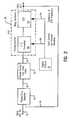
- FIG. 1depicts a conventional PLL circuit 10 which is generally comprised of a phase/frequency detector 12 , a charge pump and low pass filter 14 , a voltage controlled oscillator 16 , and if necessary, a frequency divider 18 . If the clock frequency input to the phase detector and the output frequency of the voltage controlled oscillator are equal, the frequency divider 18 is not required.
- the phase detector 12is a device which detects the difference in phase between two input signals, and produces an output signal 20 proportional to the amount of the phase difference.
- the two inputs to the phase detector 12are the input to the phase locked loop or frequency reference-in signal 22 and the output signal of the voltage controlled oscillator, i.e., the feedback or frequency-out signal 24 .
- the charge pumpproduces a control voltage based on the output signal of the phase detector and outputs the control voltage to the low pass filter.
- the charge pumpcharges and discharges a capacitor in the low pass filter, depending upon the advanced/delayed phase signal.
- the low pass filterthen eliminates the high frequency components and noise of the output voltage signal that corresponds to the phase difference.
- the low pass filtersmoothes the phase difference signal to convert the same to an error or control voltage 26 which is supplied to the VCO 16 to control the oscillation frequency.
- This low pass filter output signal 26is then fed into the voltage controlled oscillator 16 .
- the VCOis the most critical component of a phase locked loop system.
- a common implementation of a VCOconsists of a transconductor 28 and ring oscillator 30 .
- the transconductor 28converts the input voltage signal 26 into a proportional current signal 29 for input into the ring oscillator 30 .
- a gain Kvcois associated with this voltage-current (V-I) conversion.
- the output frequency dependence on the control voltageis determined by this conversion gain Kvco of the VCO.
- the center frequency of the ring oscillator 30may be modified by an external current control or by logic or digital input.
- Digital control circuitry 38is shown as a means of controlling the ring oscillator center frequency.
- the PLLis a negative feedback loop, it functions to minimize the phase difference between the oscillation signal 24 and the reference signal 22 .
- the PLL circuitreaches the lock-in point, the phases of the two signals match with one another, i.e., the oscillation phase and frequency of the VCO output signal 24 become the same as the phase and frequency of the reference signal 22 .
- Maintaining a low VCO gainis one method of reducing the noise sensitivity of the circuit.
- the gain Kvcomay also vary significantly with process, temperature, and power supply variations.
- component tolerances and process variationsalso affect the range of the center frequency settings at the voltage controlled oscillator output.
- center frequency adjustmentshave been implemented as the way to accommodate these tolerances and variations.
- the center frequency of a VCOfor component or process variations by either trimming or electronically adjusting the circuit parameters.
- the tail current of the VCOis increased in steps until the desired center frequency is reached and the PLL locks.
- the number of steps required to reach the center frequencyis an indicator of the speed of the process.
- the gain of a VCOmay also vary widely with process, and if left uncontrolled, may affect the stability and noise of the PLL circuit even with a center frequency adjustment.
- a further object of the present inventionis to ensure that a PLL circuit and its associated VCO are less susceptible to noise.
- Yet another object of the present inventionis to achieve digital gain control of a VCO without varying components.
- a voltage controlled oscillator with digital controlcomprising: a multistage current controlled oscillator responsive to a control current signal, and outputting a voltage signal having variable frequency; a transconductor for use as a voltage-to current converter having a predetermined gain, the transconductor responsive to an input voltage signal, converting the input voltage signal to the control current signal as a transconductor output with the predetermined gain, the gain adjustable by digital control circuitry; and, the digital control circuitry responsive to digital logic inputs, having control signal inputs to the transconductor, and adapted to control the gain.
- the voltage controlled oscillatorincludes a current controlled oscillator comprising a ring oscillator.
- the voltage signal having variable frequencyis further comprised of a differential transistor output; the input voltage signal is comprised of a differential transistor pair.
- the digital control circuitryis adapted to output directly to the transconductor, and to adjust and control a center frequency of the current controlled oscillator.
- the digital control circuitryfurther comprises a digitally controlled variable resistance circuit. Input to the digitally controlled variable resistance circuit comprises a digital-to-analog converter output such that the variable resistance is modified by the digital-to-analog converter output.
- the voltage controlled oscillatorfurther includes the variable resistors being adjusted according to changes in process, such that slower processes requiring more of the gain can be accommodated by an increase in the variable resistance, and faster processes requiring less of the gain can be accommodated by a decrease in the variable resistance.
- the present inventionis directed to a voltage controlled oscillator with digital control comprising: a multistage current controlled oscillator responsive to a control current signal, and outputting a voltage signal having variable frequency; a transconductor for use as a voltage-to-current converter having a predetermined gain, the transconductor responsive to an input voltage signal, converting the input voltage signal to the control current signal as a transconductor output with the predetermined gain, the gain adjustable by digital control circuitry; and, the digital control circuitry comprising a digitally controlled variable current transconductor circuit responsive to digital logic inputs, having control signal inputs to the transconductor, and adapted to control the gain.
- the voltage controlled oscillatorfurther comprises a differential transistor pair responsive to receiving the differential voltage input from the low pass filter.
- the VCOincludes fixed resistors electrically connected to the differential transistor pair and to a power supply line of the voltage controlled oscillator, and a voltage level shifter.
- the voltage level shiftercomprises a transistor circuit having an input connected to the fixed resistors, and an output connected to a PFET differential pair.
- the PFET differential pairdrives the transconductor output and directly controls the gain.
- the VCOmay further comprise a digital-to-analog converter for establishing a binary weighted amount of current for the PFET differential pair.
- the present inventionis directed to a voltage controlled oscillator with digital control comprising: a multistage current controlled oscillator responsive to a control current signal, and outputting a voltage signal having variable frequency; a transconductor for use as a voltage-to-current converter having a predetermined gain, the transconductor having an input transistor circuit including a source-coupled differential pair having a tail current, responsive to an input voltage signal, converting the input voltage signal to the control current signal as a transconductor output with the predetermined gain, the gain adjustable by digital control circuitry; and, the digital control circuitry responsive to digital logic inputs, having control signal inputs to the transconductor, and adapted to control the gain.
- the source-coupled differential pairis driven by a low pass filter capacitor output voltage, and connected to load transistors.
- the voltage controlled oscillatormay further comprise a current source and a current mirror for generating the tail current.
- the currents to the load transistorsare responsive to a change in the low pass filter capacitor output voltage, and mirrored to individual banks of transistors. The amount of current allowed to flow to the transconductor output is determined by setting a digital-to-analog converter.
- the present inventionis directed to a phase locked loop circuit comprising: a phase/frequency detector for detecting a phase difference between an oscillation signal from a voltage controlled oscillator and a reference signal; a charge pump and low pass filter circuit for receiving an output signal from the phase/frequency detector, removing high frequency components from the phase/frequency detector output signal, and outputting a control voltage signal to the voltage controlled oscillator; the voltage controlled oscillator comprising: a multistage current controlled oscillator responsive to a control current signal, and outputting a voltage signal having variable frequency; a transconductor for use as a voltage-to-current converter having a predetermined gain, the transconductor responsive to the control voltage signal, converting the control voltage signal to the control current signal as a transconductor output with the predetermined gain, the gain adjustable by digital control circuitry; and, the digital control circuitry responsive to digital logic inputs, having control signal inputs to the transconductor, and adapted to control the gain.
- FIG. 1is a block diagram of a prior art phase lock loop circuit.
- FIG. 2is a block diagram of the PLL circuit of the instant invention.
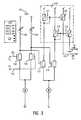
- FIG. 3is an electrical schematic of a digitally controlled variable resistance transconductor.
- FIG. 4is an electrical schematic of a digitally controlled variable current transconductor.
- FIG. 5is an electrical schematic of a digitally controlled transconductor.
- FIGS. 1-5 of the drawingsin which like numerals refer to like features of the invention.
- Features of the inventionare not necessarily shown to scale in the drawings.
- V-Ivoltage-to-current converter
- transconductorwhich changes the control voltage of the filter capacitor to a control current that varies the VCO frequency.
- the gain of the circuitcan be modified by changing the gain of the transconductor.
- a phase lock loop circuit having a voltage controlled oscillator gain digitally controlledcomprising a phase detector, a charge pump and low pass filter, a voltage controlled oscillator, and digital control circuitry for gain adjustment to the V-I converter of the voltage controlled oscillator.
- FIG. 2represents a block diagram of the present invention.
- a frequency reference signal 42is one input to the phase/frequency detector 32 .
- the second input to phase detector 42is the output signal 44 of the voltage controlled oscillator 36 .
- Output signal 44represents the feedback signal for the PLL circuit.
- the phase detectoroutputs a signal 40 proportional to the phase difference between the two input signals 42 , 44 .
- This phase detector output signal 40is received by the charge pump and low pass filter circuitry 34 .
- the control voltage signal produced by the charge pumpis fed to the low pass filter where high frequency noise components are eliminated.
- the filtered phase difference signalis converted to a voltage signal 46 which is then passed to the voltage controlled oscillator circuit 36 .
- the VCOconsists of a transconductor (V-I converter) 48 and a ring oscillator (current controlled oscillator) 50 .
- Transconductor 48converts the input voltage signal 46 into a proportional current signal for input into the ring oscillator 50 .
- the gain Kvco associated with this voltage-current (V-I) conversionis digitally controlled by digital control circuitry 52 .
- Digital control circuitry 52outputs directly to the V-I converter 48 through control signal(s) 56 .
- the digital control signalsmay also control and adjust the center frequency by accessing the ring oscillator 36 through signal(s) 54 .
- the present inventionis directly related to the digital control of the V-I converter gain for mitigating process variation, separate and distinct from the digital controlling of the ring oscillator's center frequency.
- FIG. 3represents the first embodiment of the present invention, a digitally controlled variable resistance transconductor.
- a digitally controlled variable resistanceis used to regulate and control the transconductor gain.
- the differential voltage input from the low pass filter, Vp 101 and Vn 102 , respectively,are received by an NFET differential pair 103 , 104 .
- the analog converter (DAC) 110controls the current through variable resistors 105 and 106 having control lines CNTL 0 , CNTL 1 , CNTL 2 , CNTL 3 , and the like, corresponding to each bit activated by the DAC.
- the control linesincrement the variable resistance of resistors 105 , 106 .
- variable resistors 105 , 106are adjusted according to changes in the manufacturing process.
- V-I gain of the transconductoris incrementally adjusted as an input to the ring oscillator circuitry.
- FIG. 4A second embodiment for the digitally controlled gain circuitry is depicted in FIG. 4 .
- This embodimentrepresents a variable current transconductor that reduces the chip area required to implement the design of the first embodiment.
- a differential voltage input from the low pass filter, V p 201 and V n 202 , respectivelyis received by an NFET differential pair 203 , 204 .
- Fixed resistors 205 , 206are tied to the NFET differential pair. These fixed resistors are in place of the variable resistors of the first embodiment, thus decreasing the chip area necessary to accommodate this circuit design.
- the fixed resistors 205 , 206are connected to power supply V DD 207 through PFET 208 .
- a voltage level shifter 212is introduced, connecting PFETs 214 , 216 to the fixed resistors, and PFETs 218 , 220 to the transconductor output circuitry.
- the voltage level shifter circuitryshifts the voltage down in order to drive the PFET gain.
- the voltage level shifter 212 outputs 217 , 219are connected to a PFET differential pair 222 , having PFETs 224 and 226 .
- This differential pair 222drives the V-I transconductor outputs I p 230 and I n 232 .
- a DAC 210is used to establish a binary weighted amount of current (variable current) for the PFET differential pair 222 .
- This variable current 211is adjusted by the activation of control lines CNTL 0 , CNTL 1 , CNTL 2 , CNTL 3 , and the like.
- the variable currentdrives the PFET differential pair 222 , which directly controls the transconductor gain. Consequently, in this embodiment, the transconductor gain is controllable by digital means within the VCO, and prior to the ring oscillator stage.
- FIG. 5The preferred embodiment is depicted in FIG. 5 .
- This embodimentshows a transconductor with input transistors T 3 and T 4 comprising a source-coupled differential pair 300 driven by the voltage of the low pass filter capacitor of a PLL circuit at levels V p and V n .
- the tail current of differential pair 300is provided by the current source IREF 302 and a current mirror consisting of transistors T 0 , T 1 and T 2 .
- the currents in the load transistor suite 304primarily transistors T 6 and T 7 , are correspondingly changed.
- DACdigital-to-analog converter
- DACDigital-to-analog converter
- DACconsists of four blocks 310 , 312 , 314 and 318 , wherein 310 is the digital input providing the setting from the center frequency adjustment. Shown are three input bits or control lines, but more can be used if finer granularity of control is desired. Using input 310 , current may be incrementally increased or decreased in transistor banks 312 , 314 , and 318 .
- the reference currentis mirrored through T 1 and T 5 to transistor bank 316 , encompassing transistors T 8 , T 9 , T 10 , and T 11 .
- Thisprovides current to transistor T 29 for mirroring to transistors T 30 and T 31 .
- the currents in this pathare controlled by transistor bank 318 , comprising transistors T 20 , T 21 , and T 22 .
- the purpose of transistors T 30 , T 31is to provide equal but opposite currents such that when the input voltage at V p ⁇ V n is zero, then outputs I p and I n are both zero regardless of the control setting of the DAC. This ensures that the transconductor will affect only the VCO gain and not the center frequency, which is an advantage over the embodiment in FIG. 4 .
- Mirror transistor groups T 6 , T 16 , T 17 , T 18 , T 19 and T 7 , T 12 , T 13 , T 14 , T 15are identical and can be binary weighted to give a wide range of current control.
- Mirror transistors T 5 , T 8 , T 9 , T 10 , T 11must have the same binary weighting as the other two mirrors, however, this mirror need not be identical, as long as the multiplication factor of mirror T 29 , T 30 T 31 is such that I p ⁇ and I n are both zero when V p -V n l is zero, as previously stated.
- transistor mirror banks 308 , 306are controlled by the DAC control lines to allow for switching of the variable output lines of the mirror banks. Unlike the second embodiment, no voltage level shifting is necessitated in this embodiment.
- Transistor banks 312 , 314 , and 318provide switches to turn on/off corresponding current carrying lines. Through selective digital switching of the transistors responsible for carrying the current, i.e., transistor banks 312 , 314 , and 318 , various levels of current may be screened and selected.
Landscapes
- Stabilization Of Oscillater, Synchronisation, Frequency Synthesizers (AREA)
Abstract
Description
Claims (19)
Priority Applications (1)
| Application Number | Priority Date | Filing Date | Title |
|---|---|---|---|
| US09/757,107US6466100B2 (en) | 2001-01-08 | 2001-01-08 | Linear voltage controlled oscillator transconductor with gain compensation |
Applications Claiming Priority (1)
| Application Number | Priority Date | Filing Date | Title |
|---|---|---|---|
| US09/757,107US6466100B2 (en) | 2001-01-08 | 2001-01-08 | Linear voltage controlled oscillator transconductor with gain compensation |
Publications (2)
| Publication Number | Publication Date |
|---|---|
| US20020089381A1 US20020089381A1 (en) | 2002-07-11 |
| US6466100B2true US6466100B2 (en) | 2002-10-15 |
Family
ID=25046378
Family Applications (1)
| Application Number | Title | Priority Date | Filing Date |
|---|---|---|---|
| US09/757,107Expired - LifetimeUS6466100B2 (en) | 2001-01-08 | 2001-01-08 | Linear voltage controlled oscillator transconductor with gain compensation |
Country Status (1)
| Country | Link |
|---|---|
| US (1) | US6466100B2 (en) |
Cited By (29)
| Publication number | Priority date | Publication date | Assignee | Title |
|---|---|---|---|---|
| US20010016476A1 (en)* | 2000-02-23 | 2001-08-23 | Masumi Kasahara | Wireless communication system |
| US6621360B1 (en)* | 2002-01-22 | 2003-09-16 | Pmc-Sierra, Inc. | Extended frequency range voltage-controlled oscillator |
| US20030197570A1 (en)* | 2002-04-19 | 2003-10-23 | Kim Kwi-Dong | Adaptive loop gain control circuit for voltage controlled oscillator |
| US20030227337A1 (en)* | 2002-06-06 | 2003-12-11 | Siniscalchi Patrick Peter | Voltage controlled oscillator having control current compensation |
| US6683502B1 (en)* | 2002-03-12 | 2004-01-27 | Xilinx, Inc. | Process compensated phase locked loop |
| US6683506B2 (en)* | 2002-01-18 | 2004-01-27 | The Regents Of The University Of California | CMOS phase locked loop with voltage controlled oscillator having realignment to reference and method for the same |
| US20040145421A1 (en)* | 2003-01-23 | 2004-07-29 | Ess Technology, Inc. | Frequency locked loop with improved stability |
| US20040239369A1 (en)* | 2003-05-30 | 2004-12-02 | International Business Machines Corporation | Programmable peaking receiver and method |
| US20050046497A1 (en)* | 2003-08-13 | 2005-03-03 | Renesas Technology Corp. | Synchronous clock generation circuit capable of ensuring wide lock-in range and attaining lower jitter |
| US20050110580A1 (en)* | 2003-07-18 | 2005-05-26 | Samsung Electronics Co., Ltd. | PLL having a multi-level voltage-current converter and a method for locking a clock phase using multi-level voltage-current conversion |
| US20060119442A1 (en)* | 2004-12-08 | 2006-06-08 | Via Technologies, Inc. | System and method for optimizing phase locked loop damping coefficient |
| US20060119441A1 (en)* | 2004-12-08 | 2006-06-08 | Via Technologies, Inc. | Phase locked loop damping coefficient correction mechanism |
| US20060139106A1 (en)* | 2004-12-24 | 2006-06-29 | Matsushita Electric Industrial Co., Ltd. | Phase-locked loop circuit |
| US20060139110A1 (en)* | 2004-12-14 | 2006-06-29 | Qiang Li | Method to compensate the VCO buffer Q factor at low frequency band |
| US20060146956A1 (en)* | 2005-01-04 | 2006-07-06 | Jae-Wan Kim | RF transmitter for efficiently compensating output power variation due to temperature and process |
| US20060197614A1 (en)* | 2005-03-01 | 2006-09-07 | Regis Roubadia | Multi-phase realigned voltage-controlled oscillator and phase-locked loop incorporating the same |
| US7148758B1 (en)* | 2004-08-13 | 2006-12-12 | Xilinx, Inc. | Integrated circuit with digitally controlled phase-locked loop |
| US20070013455A1 (en)* | 2005-07-18 | 2007-01-18 | Atmel Corporation | Voltage-controlled oscillator with multi-phase realignment of asymmetric stages |
| US20070133729A1 (en)* | 2005-12-12 | 2007-06-14 | Chiao-Wei Hsiao | Spread ratio fixing circuit and method for generating spread spectrum clock |
| US20080186066A1 (en)* | 2006-01-10 | 2008-08-07 | Samsung Electronics Co., Ltd. | Phase locked loop and phase locking method |
| US7636014B1 (en) | 2008-07-04 | 2009-12-22 | Holtek Semiconductor Inc. | Digitally programmable transconductance amplifier and mixed-signal circuit using the same |
| US20100001804A1 (en)* | 2008-07-06 | 2010-01-07 | Friend David M | System to improve a voltage-controlled oscillator and associated methods |
| US20100194482A1 (en)* | 2009-02-05 | 2010-08-05 | International Business Machines Corporation | Compensation of vco gain curve offsets using auto-calibration |
| US20100194483A1 (en)* | 2009-02-05 | 2010-08-05 | International Business Machines Corporation | Auto-calibration for ring oscillator vco |
| US20100259300A1 (en)* | 2009-04-08 | 2010-10-14 | Broadcom Corporation | Circuit for digitally controlling line driver current |
| CN1976232B (en)* | 2005-12-08 | 2011-04-13 | 威盛电子股份有限公司 | Device and method for adjusting damping coefficient in phase-locked loop |
| CN101626221B (en)* | 2008-07-11 | 2012-03-28 | 盛群半导体股份有限公司 | Digital programmable transconductance amplifier and mixed signal circuit using the amplifier |
| US20120293222A1 (en)* | 2006-11-27 | 2012-11-22 | Fujitsu Semiconductor Limited | Pll circuit |
| US11095297B2 (en) | 2019-06-10 | 2021-08-17 | Stmicroelectronics International N.V. | Phase locked loop (PLL) circuit with voltage controlled oscillator (VCO) having reduced gain |
Families Citing this family (5)
| Publication number | Priority date | Publication date | Assignee | Title |
|---|---|---|---|---|
| US8340215B2 (en)* | 2002-07-26 | 2012-12-25 | Motorola Mobility Llc | Radio transceiver architectures and methods |
| US6882237B2 (en) | 2003-04-30 | 2005-04-19 | Zarlink Semiconductor Inc. | Capture range control mechanism for voltage controlled oscillators |
| JP2012191745A (en)* | 2011-03-10 | 2012-10-04 | Semiconductor Components Industries Llc | Power circuit system |
| US9065457B2 (en)* | 2012-04-26 | 2015-06-23 | Skyworks Solutions, Inc. | Circuits and methods for eliminating reference spurs in fractional-N frequency synthesis |
| US8917146B1 (en)* | 2014-02-18 | 2014-12-23 | King Fahd University Of Petroleum And Minerals | Current-controlled operational transconductance amplifier based sinusoidal oscillator circuit |
Citations (11)
| Publication number | Priority date | Publication date | Assignee | Title |
|---|---|---|---|---|
| US5061907A (en) | 1991-01-17 | 1991-10-29 | National Semiconductor Corporation | High frequency CMOS VCO with gain constant and duty cycle compensation |
| US5382922A (en) | 1993-12-23 | 1995-01-17 | International Business Machines Corporation | Calibration systems and methods for setting PLL gain characteristics and center frequency |
| US5422911A (en)* | 1993-09-17 | 1995-06-06 | Motorola, Inc. | Frequency walled phase lock loop |
| US5495512A (en)* | 1994-09-12 | 1996-02-27 | Analog Devices, Inc. | Hybrid phase locked loop |
| US5933031A (en) | 1997-02-05 | 1999-08-03 | Mitsubishi Denki Kabushiki Kaisha | Phase locked loop circuit with reduced electrical power consumption |
| US5933037A (en) | 1997-08-29 | 1999-08-03 | Adaptec, Inc. | High speed phase lock loop having constant bandwidth |
| US5973572A (en) | 1997-03-19 | 1999-10-26 | Advantest Corp. | Phase lock loop circuit with variable loop gain |
| US5982213A (en) | 1997-11-14 | 1999-11-09 | Texas Instruments Incorporated | Digital phase lock loop |
| US6028727A (en)* | 1997-09-05 | 2000-02-22 | Cirrus Logic, Inc. | Method and system to improve single synthesizer setting times for small frequency steps in read channel circuits |
| US6084480A (en) | 1997-08-07 | 2000-07-04 | Nec Corporation | Phase locked loop circuit including voltage controlled oscillator and low pass filter |
| US6266200B1 (en)* | 1989-10-30 | 2001-07-24 | Hitachi, Ltd | Magnetic disk storage apparatus |
- 2001
- 2001-01-08USUS09/757,107patent/US6466100B2/ennot_activeExpired - Lifetime
Patent Citations (11)
| Publication number | Priority date | Publication date | Assignee | Title |
|---|---|---|---|---|
| US6266200B1 (en)* | 1989-10-30 | 2001-07-24 | Hitachi, Ltd | Magnetic disk storage apparatus |
| US5061907A (en) | 1991-01-17 | 1991-10-29 | National Semiconductor Corporation | High frequency CMOS VCO with gain constant and duty cycle compensation |
| US5422911A (en)* | 1993-09-17 | 1995-06-06 | Motorola, Inc. | Frequency walled phase lock loop |
| US5382922A (en) | 1993-12-23 | 1995-01-17 | International Business Machines Corporation | Calibration systems and methods for setting PLL gain characteristics and center frequency |
| US5495512A (en)* | 1994-09-12 | 1996-02-27 | Analog Devices, Inc. | Hybrid phase locked loop |
| US5933031A (en) | 1997-02-05 | 1999-08-03 | Mitsubishi Denki Kabushiki Kaisha | Phase locked loop circuit with reduced electrical power consumption |
| US5973572A (en) | 1997-03-19 | 1999-10-26 | Advantest Corp. | Phase lock loop circuit with variable loop gain |
| US6084480A (en) | 1997-08-07 | 2000-07-04 | Nec Corporation | Phase locked loop circuit including voltage controlled oscillator and low pass filter |
| US5933037A (en) | 1997-08-29 | 1999-08-03 | Adaptec, Inc. | High speed phase lock loop having constant bandwidth |
| US6028727A (en)* | 1997-09-05 | 2000-02-22 | Cirrus Logic, Inc. | Method and system to improve single synthesizer setting times for small frequency steps in read channel circuits |
| US5982213A (en) | 1997-11-14 | 1999-11-09 | Texas Instruments Incorporated | Digital phase lock loop |
Cited By (49)
| Publication number | Priority date | Publication date | Assignee | Title |
|---|---|---|---|---|
| US7162216B2 (en) | 2000-02-23 | 2007-01-09 | Renesas Technology Corp. | Wireless communication system |
| US20010016476A1 (en)* | 2000-02-23 | 2001-08-23 | Masumi Kasahara | Wireless communication system |
| US20070087716A1 (en)* | 2000-02-23 | 2007-04-19 | Masumi Kasahara | Wireless communication system |
| US6714772B2 (en)* | 2000-02-23 | 2004-03-30 | Renesas Technology Corp. | Wireless communication system |
| US6683506B2 (en)* | 2002-01-18 | 2004-01-27 | The Regents Of The University Of California | CMOS phase locked loop with voltage controlled oscillator having realignment to reference and method for the same |
| US6621360B1 (en)* | 2002-01-22 | 2003-09-16 | Pmc-Sierra, Inc. | Extended frequency range voltage-controlled oscillator |
| US6683502B1 (en)* | 2002-03-12 | 2004-01-27 | Xilinx, Inc. | Process compensated phase locked loop |
| US20030197570A1 (en)* | 2002-04-19 | 2003-10-23 | Kim Kwi-Dong | Adaptive loop gain control circuit for voltage controlled oscillator |
| US6833766B2 (en)* | 2002-04-19 | 2004-12-21 | Electronics And Telecommunications Research Institute | Adaptive loop gain control circuit for voltage controlled oscillator |
| US20030227337A1 (en)* | 2002-06-06 | 2003-12-11 | Siniscalchi Patrick Peter | Voltage controlled oscillator having control current compensation |
| US6949984B2 (en)* | 2002-06-06 | 2005-09-27 | Texas Instruments Incorporated | Voltage controlled oscillator having control current compensation |
| WO2004068712A1 (en)* | 2003-01-23 | 2004-08-12 | Ess Technology, Inc. | Frequency locked loop with improved stability |
| US6833765B2 (en) | 2003-01-23 | 2004-12-21 | Ess Technology, Inc. | Frequency locked loop with improved stability using binary rate multiplier circuits |
| US20040145421A1 (en)* | 2003-01-23 | 2004-07-29 | Ess Technology, Inc. | Frequency locked loop with improved stability |
| US6937054B2 (en) | 2003-05-30 | 2005-08-30 | International Business Machines Corporation | Programmable peaking receiver and method |
| US20040239369A1 (en)* | 2003-05-30 | 2004-12-02 | International Business Machines Corporation | Programmable peaking receiver and method |
| US7068111B2 (en)* | 2003-07-18 | 2006-06-27 | Samsung Electronics Co., Ltd. | PLL having a multi-level voltage-current converter and a method for locking a clock phase using multi-level voltage-current conversion |
| US20050110580A1 (en)* | 2003-07-18 | 2005-05-26 | Samsung Electronics Co., Ltd. | PLL having a multi-level voltage-current converter and a method for locking a clock phase using multi-level voltage-current conversion |
| US20050046497A1 (en)* | 2003-08-13 | 2005-03-03 | Renesas Technology Corp. | Synchronous clock generation circuit capable of ensuring wide lock-in range and attaining lower jitter |
| US7064621B2 (en)* | 2003-08-13 | 2006-06-20 | Renesas Technology Corp. | Synchronous clock generation circuit capable of ensuring wide lock-in range and attaining lower jitter |
| US7148758B1 (en)* | 2004-08-13 | 2006-12-12 | Xilinx, Inc. | Integrated circuit with digitally controlled phase-locked loop |
| US20060119441A1 (en)* | 2004-12-08 | 2006-06-08 | Via Technologies, Inc. | Phase locked loop damping coefficient correction mechanism |
| US20060119442A1 (en)* | 2004-12-08 | 2006-06-08 | Via Technologies, Inc. | System and method for optimizing phase locked loop damping coefficient |
| US20060139110A1 (en)* | 2004-12-14 | 2006-06-29 | Qiang Li | Method to compensate the VCO buffer Q factor at low frequency band |
| US20060139106A1 (en)* | 2004-12-24 | 2006-06-29 | Matsushita Electric Industrial Co., Ltd. | Phase-locked loop circuit |
| US7298219B2 (en) | 2004-12-24 | 2007-11-20 | Matsushita Electric Industrial Co., Ltd. | Phase-locked loop circuit |
| US20060146956A1 (en)* | 2005-01-04 | 2006-07-06 | Jae-Wan Kim | RF transmitter for efficiently compensating output power variation due to temperature and process |
| US7564922B2 (en)* | 2005-01-04 | 2009-07-21 | Samsung Electronics Co., Ltd. | RF transmitter for efficiently compensating output power variation due to temperature and process |
| US7126432B2 (en) | 2005-03-01 | 2006-10-24 | Atmel Corporation | Multi-phase realigned voltage-controlled oscillator and phase-locked loop incorporating the same |
| US20060197614A1 (en)* | 2005-03-01 | 2006-09-07 | Regis Roubadia | Multi-phase realigned voltage-controlled oscillator and phase-locked loop incorporating the same |
| US20070013455A1 (en)* | 2005-07-18 | 2007-01-18 | Atmel Corporation | Voltage-controlled oscillator with multi-phase realignment of asymmetric stages |
| US7339439B2 (en) | 2005-07-18 | 2008-03-04 | Atmel Corporation | Voltage-controlled oscillator with multi-phase realignment of asymmetric stages |
| CN1976232B (en)* | 2005-12-08 | 2011-04-13 | 威盛电子股份有限公司 | Device and method for adjusting damping coefficient in phase-locked loop |
| US20070133729A1 (en)* | 2005-12-12 | 2007-06-14 | Chiao-Wei Hsiao | Spread ratio fixing circuit and method for generating spread spectrum clock |
| US7764092B2 (en)* | 2006-01-10 | 2010-07-27 | Samsung Electronics Co., Ltd. | Phase locked loop and phase locking method |
| US20080186066A1 (en)* | 2006-01-10 | 2008-08-07 | Samsung Electronics Co., Ltd. | Phase locked loop and phase locking method |
| US8638140B2 (en)* | 2006-11-27 | 2014-01-28 | Spansion Llc | PLL circuit |
| US20120293222A1 (en)* | 2006-11-27 | 2012-11-22 | Fujitsu Semiconductor Limited | Pll circuit |
| US20100001798A1 (en)* | 2008-07-04 | 2010-01-07 | Holtek Semiconductor Inc. | Digitally programmable transconductance amplifier and mixed-signal circuit using the same |
| US7636014B1 (en) | 2008-07-04 | 2009-12-22 | Holtek Semiconductor Inc. | Digitally programmable transconductance amplifier and mixed-signal circuit using the same |
| US20100001804A1 (en)* | 2008-07-06 | 2010-01-07 | Friend David M | System to improve a voltage-controlled oscillator and associated methods |
| CN101626221B (en)* | 2008-07-11 | 2012-03-28 | 盛群半导体股份有限公司 | Digital programmable transconductance amplifier and mixed signal circuit using the amplifier |
| US20100194483A1 (en)* | 2009-02-05 | 2010-08-05 | International Business Machines Corporation | Auto-calibration for ring oscillator vco |
| US8183949B2 (en) | 2009-02-05 | 2012-05-22 | International Business Machines Corporation | Compensation of VCO gain curve offsets using auto-calibration |
| US8183950B2 (en) | 2009-02-05 | 2012-05-22 | International Business Machines Corporation | Auto-calibration for ring oscillator VCO |
| US20100194482A1 (en)* | 2009-02-05 | 2010-08-05 | International Business Machines Corporation | Compensation of vco gain curve offsets using auto-calibration |
| US8183885B2 (en)* | 2009-04-08 | 2012-05-22 | Broadcom Corporation | Circuit for digitally controlling line driver current |
| US20100259300A1 (en)* | 2009-04-08 | 2010-10-14 | Broadcom Corporation | Circuit for digitally controlling line driver current |
| US11095297B2 (en) | 2019-06-10 | 2021-08-17 | Stmicroelectronics International N.V. | Phase locked loop (PLL) circuit with voltage controlled oscillator (VCO) having reduced gain |
Also Published As
| Publication number | Publication date |
|---|---|
| US20020089381A1 (en) | 2002-07-11 |
Similar Documents
| Publication | Publication Date | Title |
|---|---|---|
| US6466100B2 (en) | Linear voltage controlled oscillator transconductor with gain compensation | |
| US6222421B1 (en) | Phase-locked loop | |
| US5691669A (en) | Dual adjust current controlled phase locked loop | |
| US8111093B2 (en) | Power supply noise rejection in PLL or DLL circuits | |
| US5740213A (en) | Differential charge pump based phase locked loop or delay locked loop | |
| US6777991B2 (en) | Method and apparatus for stable phase-locked looping | |
| US6781425B2 (en) | Current-steering charge pump circuit and method of switching | |
| FI92120B (en) | Voltage controlled oscillator | |
| US7924102B2 (en) | Symmetric load delay cell oscillator | |
| US6873214B2 (en) | Use of configurable capacitors to tune a self biased phase locked loop | |
| US20080218277A1 (en) | Apparatus and method for operating a phase-locked loop circuit | |
| US7382203B2 (en) | Voltage controlled oscillator and delay circuit thereof | |
| US6526111B1 (en) | Method and apparatus for phase locked loop having reduced jitter and/or frequency biasing | |
| US10911053B2 (en) | Phase locked loop design with reduced VCO gain | |
| JP2002353809A (en) | Clock generation circuit | |
| US6624668B1 (en) | Digitally programmable phase-lock loop for high-speed data communications | |
| US5739725A (en) | Digitally controlled oscillator circuit | |
| US5459653A (en) | Voltage to current converter with independent loop gain and frequency control | |
| US6642799B2 (en) | Phase lock loop destress circuit | |
| GB2319917A (en) | Voltage controlled oscillator | |
| US20220166381A1 (en) | Circuit for extended voltage control oscillator gain linearity | |
| US6621360B1 (en) | Extended frequency range voltage-controlled oscillator | |
| KR20070074698A (en) | Gain-Adjustable Ring Oscillator Oscillator and Method | |
| EP4572148A1 (en) | Systems, methods, and apparatus for controlling oscillator frequency response | |
| US7746177B2 (en) | Self-biased bipolar ring-oscillator phase-locked loops with wide tuning range |
Legal Events
| Date | Code | Title | Description |
|---|---|---|---|
| AS | Assignment | Owner name:INTERNATIONAL BUSINESS MACHINES CORPORATION, NEW Y Free format text:ASSIGNMENT OF ASSIGNORS INTEREST;ASSIGNORS:MULLGRAV, ALLAN L. JR.;SORNA, MICHAEL A.;REEL/FRAME:011448/0653 Effective date:20001205 | |
| STCF | Information on status: patent grant | Free format text:PATENTED CASE | |
| FPAY | Fee payment | Year of fee payment:4 | |
| FPAY | Fee payment | Year of fee payment:8 | |
| REMI | Maintenance fee reminder mailed | ||
| FPAY | Fee payment | Year of fee payment:12 | |
| SULP | Surcharge for late payment | Year of fee payment:11 | |
| AS | Assignment | Owner name:GLOBALFOUNDRIES U.S. 2 LLC, NEW YORK Free format text:ASSIGNMENT OF ASSIGNORS INTEREST;ASSIGNOR:INTERNATIONAL BUSINESS MACHINES CORPORATION;REEL/FRAME:036550/0001 Effective date:20150629 | |
| AS | Assignment | Owner name:GLOBALFOUNDRIES INC., CAYMAN ISLANDS Free format text:ASSIGNMENT OF ASSIGNORS INTEREST;ASSIGNORS:GLOBALFOUNDRIES U.S. 2 LLC;GLOBALFOUNDRIES U.S. INC.;REEL/FRAME:036779/0001 Effective date:20150910 | |
| AS | Assignment | Owner name:WILMINGTON TRUST, NATIONAL ASSOCIATION, DELAWARE Free format text:SECURITY AGREEMENT;ASSIGNOR:GLOBALFOUNDRIES INC.;REEL/FRAME:049490/0001 Effective date:20181127 | |
| AS | Assignment | Owner name:GLOBALFOUNDRIES U.S. INC., CALIFORNIA Free format text:ASSIGNMENT OF ASSIGNORS INTEREST;ASSIGNOR:GLOBALFOUNDRIES INC.;REEL/FRAME:050122/0001 Effective date:20190821 | |
| AS | Assignment | Owner name:MARVELL INTERNATIONAL LTD., BERMUDA Free format text:ASSIGNMENT OF ASSIGNORS INTEREST;ASSIGNOR:GLOBALFOUNDRIES U.S. INC.;REEL/FRAME:051070/0625 Effective date:20191105 | |
| AS | Assignment | Owner name:CAVIUM INTERNATIONAL, CAYMAN ISLANDS Free format text:ASSIGNMENT OF ASSIGNORS INTEREST;ASSIGNOR:MARVELL INTERNATIONAL LTD.;REEL/FRAME:052918/0001 Effective date:20191231 | |
| AS | Assignment | Owner name:MARVELL ASIA PTE, LTD., SINGAPORE Free format text:ASSIGNMENT OF ASSIGNORS INTEREST;ASSIGNOR:CAVIUM INTERNATIONAL;REEL/FRAME:053475/0001 Effective date:20191231 | |
| AS | Assignment | Owner name:GLOBALFOUNDRIES INC., CAYMAN ISLANDS Free format text:RELEASE BY SECURED PARTY;ASSIGNOR:WILMINGTON TRUST, NATIONAL ASSOCIATION;REEL/FRAME:054636/0001 Effective date:20201117 |