US6466047B1 - System for testing bumped semiconductor components with on-board multiplex circuit for expanding tester resources - Google Patents
System for testing bumped semiconductor components with on-board multiplex circuit for expanding tester resourcesDownload PDFInfo
- Publication number
- US6466047B1 US6466047B1US09/999,502US99950201AUS6466047B1US 6466047 B1US6466047 B1US 6466047B1US 99950201 AUS99950201 AUS 99950201AUS 6466047 B1US6466047 B1US 6466047B1
- Authority
- US
- United States
- Prior art keywords
- interconnect
- contacts
- test
- test system
- components
- Prior art date
- Legal status (The legal status is an assumption and is not a legal conclusion. Google has not performed a legal analysis and makes no representation as to the accuracy of the status listed.)
- Expired - Lifetime
Links
- 238000012360testing methodMethods0.000titleclaimsabstractdescription189
- 239000004065semiconductorSubstances0.000titleclaimsabstractdescription53
- 239000000758substrateSubstances0.000claimsabstractdescription82
- 238000004891communicationMethods0.000claimsdescription28
- 239000000463materialSubstances0.000claimsdescription14
- 229910000679solderInorganic materials0.000claimsdescription8
- 230000000149penetrating effectEffects0.000claimsdescription6
- 235000012431wafersNutrition0.000abstractdescription36
- 238000010998test methodMethods0.000abstractdescription7
- 230000002950deficientEffects0.000abstractdescription5
- 239000010410layerSubstances0.000description34
- 239000004020conductorSubstances0.000description28
- 238000000034methodMethods0.000description26
- 230000008569processEffects0.000description15
- 229910052751metalInorganic materials0.000description13
- 239000002184metalSubstances0.000description13
- XUIMIQQOPSSXEZ-UHFFFAOYSA-NSiliconChemical compound[Si]XUIMIQQOPSSXEZ-UHFFFAOYSA-N0.000description11
- 229910052710siliconInorganic materials0.000description11
- 239000010703siliconSubstances0.000description11
- 239000012528membraneSubstances0.000description8
- 239000000523sampleSubstances0.000description8
- 238000005530etchingMethods0.000description6
- 238000004519manufacturing processMethods0.000description6
- 238000001465metallisationMethods0.000description6
- 238000010586diagramMethods0.000description5
- 238000003491arrayMethods0.000description4
- 239000004642PolyimideSubstances0.000description3
- 239000000919ceramicSubstances0.000description3
- 239000011521glassSubstances0.000description3
- 150000002739metalsChemical class0.000description3
- 230000002093peripheral effectEffects0.000description3
- 229920001721polyimidePolymers0.000description3
- 229920005989resinPolymers0.000description3
- 239000011347resinSubstances0.000description3
- 238000012956testing procedureMethods0.000description3
- JBRZTFJDHDCESZ-UHFFFAOYSA-NAsGaChemical compound[As]#[Ga]JBRZTFJDHDCESZ-UHFFFAOYSA-N0.000description2
- RYGMFSIKBFXOCR-UHFFFAOYSA-NCopperChemical compound[Cu]RYGMFSIKBFXOCR-UHFFFAOYSA-N0.000description2
- 229910001218Gallium arsenideInorganic materials0.000description2
- ZOKXTWBITQBERF-UHFFFAOYSA-NMolybdenumChemical compound[Mo]ZOKXTWBITQBERF-UHFFFAOYSA-N0.000description2
- PXHVJJICTQNCMI-UHFFFAOYSA-NNickelChemical compound[Ni]PXHVJJICTQNCMI-UHFFFAOYSA-N0.000description2
- KDLHZDBZIXYQEI-UHFFFAOYSA-NPalladiumChemical compound[Pd]KDLHZDBZIXYQEI-UHFFFAOYSA-N0.000description2
- VYPSYNLAJGMNEJ-UHFFFAOYSA-NSilicium dioxideChemical compoundO=[Si]=OVYPSYNLAJGMNEJ-UHFFFAOYSA-N0.000description2
- RTAQQCXQSZGOHL-UHFFFAOYSA-NTitaniumChemical compound[Ti]RTAQQCXQSZGOHL-UHFFFAOYSA-N0.000description2
- 239000012790adhesive layerSubstances0.000description2
- 229910045601alloyInorganic materials0.000description2
- 239000000956alloySubstances0.000description2
- 229910052782aluminiumInorganic materials0.000description2
- XAGFODPZIPBFFR-UHFFFAOYSA-NaluminiumChemical compound[Al]XAGFODPZIPBFFR-UHFFFAOYSA-N0.000description2
- 229910052802copperInorganic materials0.000description2
- 239000010949copperSubstances0.000description2
- 230000013011matingEffects0.000description2
- 230000007246mechanismEffects0.000description2
- 229910052750molybdenumInorganic materials0.000description2
- 239000011733molybdenumSubstances0.000description2
- 230000035515penetrationEffects0.000description2
- BASFCYQUMIYNBI-UHFFFAOYSA-NplatinumChemical compound[Pt]BASFCYQUMIYNBI-UHFFFAOYSA-N0.000description2
- 229920000642polymerPolymers0.000description2
- 229920001296polysiloxanePolymers0.000description2
- 229910052715tantalumInorganic materials0.000description2
- GUVRBAGPIYLISA-UHFFFAOYSA-Ntantalum atomChemical compound[Ta]GUVRBAGPIYLISA-UHFFFAOYSA-N0.000description2
- 239000010936titaniumSubstances0.000description2
- 229910052719titaniumInorganic materials0.000description2
- WFKWXMTUELFFGS-UHFFFAOYSA-NtungstenChemical compound[W]WFKWXMTUELFFGS-UHFFFAOYSA-N0.000description2
- 229910052721tungstenInorganic materials0.000description2
- 239000010937tungstenSubstances0.000description2
- JYEUMXHLPRZUAT-UHFFFAOYSA-N1,2,3-triazineChemical compoundC1=CN=NN=C1JYEUMXHLPRZUAT-UHFFFAOYSA-N0.000description1
- XQUPVDVFXZDTLT-UHFFFAOYSA-N1-[4-[[4-(2,5-dioxopyrrol-1-yl)phenyl]methyl]phenyl]pyrrole-2,5-dioneChemical compoundO=C1C=CC(=O)N1C(C=C1)=CC=C1CC1=CC=C(N2C(C=CC2=O)=O)C=C1XQUPVDVFXZDTLT-UHFFFAOYSA-N0.000description1
- 239000004593EpoxySubstances0.000description1
- JOYRKODLDBILNP-UHFFFAOYSA-NEthyl urethaneChemical compoundCCOC(N)=OJOYRKODLDBILNP-UHFFFAOYSA-N0.000description1
- 239000004793PolystyreneSubstances0.000description1
- BQCADISMDOOEFD-UHFFFAOYSA-NSilverChemical compound[Ag]BQCADISMDOOEFD-UHFFFAOYSA-N0.000description1
- BOTDANWDWHJENH-UHFFFAOYSA-NTetraethyl orthosilicateChemical compoundCCO[Si](OCC)(OCC)OCCBOTDANWDWHJENH-UHFFFAOYSA-N0.000description1
- 230000004888barrier functionEffects0.000description1
- 230000005540biological transmissionEffects0.000description1
- 230000015572biosynthetic processEffects0.000description1
- 239000005380borophosphosilicate glassSubstances0.000description1
- 229920005549butyl rubberPolymers0.000description1
- 229910052681coesiteInorganic materials0.000description1
- 239000002537cosmeticSubstances0.000description1
- 229910052906cristobaliteInorganic materials0.000description1
- 238000013461designMethods0.000description1
- 239000002019doping agentSubstances0.000description1
- 239000013536elastomeric materialSubstances0.000description1
- 239000012777electrically insulating materialSubstances0.000description1
- 239000008393encapsulating agentSubstances0.000description1
- 239000003822epoxy resinSubstances0.000description1
- 239000010408filmSubstances0.000description1
- 239000006260foamSubstances0.000description1
- 239000000499gelSubstances0.000description1
- PCHJSUWPFVWCPO-UHFFFAOYSA-NgoldChemical compound[Au]PCHJSUWPFVWCPO-UHFFFAOYSA-N0.000description1
- 229910052737goldInorganic materials0.000description1
- 239000010931goldSubstances0.000description1
- 238000010438heat treatmentMethods0.000description1
- 238000009413insulationMethods0.000description1
- 229910052741iridiumInorganic materials0.000description1
- GKOZUEZYRPOHIO-UHFFFAOYSA-Niridium atomChemical compound[Ir]GKOZUEZYRPOHIO-UHFFFAOYSA-N0.000description1
- 238000012986modificationMethods0.000description1
- 230000004048modificationEffects0.000description1
- 229910052759nickelInorganic materials0.000description1
- 150000004767nitridesChemical class0.000description1
- 229910052763palladiumInorganic materials0.000description1
- 238000002161passivationMethods0.000description1
- 238000000059patterningMethods0.000description1
- 238000000206photolithographyMethods0.000description1
- 229910052697platinumInorganic materials0.000description1
- 229920003192poly(bis maleimide)Polymers0.000description1
- 229920003223poly(pyromellitimide-1,4-diphenyl ether)Polymers0.000description1
- 229920000515polycarbonatePolymers0.000description1
- 239000004417polycarbonateSubstances0.000description1
- 229910021420polycrystalline siliconInorganic materials0.000description1
- 229920000647polyepoxidePolymers0.000description1
- 229920000728polyesterPolymers0.000description1
- 239000002861polymer materialSubstances0.000description1
- 229920005591polysiliconPolymers0.000description1
- 229920002223polystyrenePolymers0.000description1
- 230000004044responseEffects0.000description1
- 238000007650screen-printingMethods0.000description1
- 229910021332silicideInorganic materials0.000description1
- FVBUAEGBCNSCDD-UHFFFAOYSA-Nsilicide(4-)Chemical compound[Si-4]FVBUAEGBCNSCDD-UHFFFAOYSA-N0.000description1
- 239000000377silicon dioxideSubstances0.000description1
- 229910052709silverInorganic materials0.000description1
- 239000004332silverSubstances0.000description1
- 239000002356single layerSubstances0.000description1
- 239000007787solidSubstances0.000description1
- 125000006850spacer groupChemical group0.000description1
- 229910052682stishoviteInorganic materials0.000description1
- 239000010409thin filmSubstances0.000description1
- 229910052905tridymiteInorganic materials0.000description1
- 239000011800void materialSubstances0.000description1
Images


Classifications
- G—PHYSICS
- G01—MEASURING; TESTING
- G01R—MEASURING ELECTRIC VARIABLES; MEASURING MAGNETIC VARIABLES
- G01R1/00—Details of instruments or arrangements of the types included in groups G01R5/00 - G01R13/00 and G01R31/00
- G01R1/02—General constructional details
- G01R1/06—Measuring leads; Measuring probes
- G01R1/067—Measuring probes
- G01R1/073—Multiple probes
- G01R1/07307—Multiple probes with individual probe elements, e.g. needles, cantilever beams or bump contacts, fixed in relation to each other, e.g. bed of nails fixture or probe card
- G01R1/07364—Multiple probes with individual probe elements, e.g. needles, cantilever beams or bump contacts, fixed in relation to each other, e.g. bed of nails fixture or probe card with provisions for altering position, number or connection of probe tips; Adapting to differences in pitch
- G01R1/07385—Multiple probes with individual probe elements, e.g. needles, cantilever beams or bump contacts, fixed in relation to each other, e.g. bed of nails fixture or probe card with provisions for altering position, number or connection of probe tips; Adapting to differences in pitch using switching of signals between probe tips and test bed, i.e. the standard contact matrix which in its turn connects to the tester
- G—PHYSICS
- G01—MEASURING; TESTING
- G01R—MEASURING ELECTRIC VARIABLES; MEASURING MAGNETIC VARIABLES
- G01R1/00—Details of instruments or arrangements of the types included in groups G01R5/00 - G01R13/00 and G01R31/00
- G01R1/02—General constructional details
- G01R1/06—Measuring leads; Measuring probes
- G01R1/067—Measuring probes
- G01R1/073—Multiple probes
- G01R1/07307—Multiple probes with individual probe elements, e.g. needles, cantilever beams or bump contacts, fixed in relation to each other, e.g. bed of nails fixture or probe card
- G01R1/07314—Multiple probes with individual probe elements, e.g. needles, cantilever beams or bump contacts, fixed in relation to each other, e.g. bed of nails fixture or probe card the body of the probe being perpendicular to test object, e.g. bed of nails or probe with bump contacts on a rigid support
- G—PHYSICS
- G01—MEASURING; TESTING
- G01R—MEASURING ELECTRIC VARIABLES; MEASURING MAGNETIC VARIABLES
- G01R31/00—Arrangements for testing electric properties; Arrangements for locating electric faults; Arrangements for electrical testing characterised by what is being tested not provided for elsewhere
- G01R31/28—Testing of electronic circuits, e.g. by signal tracer
- G01R31/282—Testing of electronic circuits specially adapted for particular applications not provided for elsewhere
- G01R31/2831—Testing of materials or semi-finished products, e.g. semiconductor wafers or substrates
Definitions
- This inventionrelates generally to semiconductor manufacture, and specifically to an interconnect and system for testing bumped semiconductor components, such as bumped semiconductor dice contained on wafers, or bumped semiconductor packages contained on panels. This invention also relates to test systems and test methods employing the interconnect.
- Semiconductor componentssuch as dice, wafers, chip scale packages, and BGA devices can include terminal contacts in the form of bumps, or balls. This type of component is sometimes referred to as a “bumped” component, and the terminal contacts are sometimes referred to as “bumped contacts”.
- the bumped contactsprovide a high input/output capability for a component, and permit the component to be surface mounted, or alternately flip chip mounted, to a mating substrate, such as a printed circuit board (PCB).
- the bumped contactscomprise solder balls, which permits bonding to the mating substrate using a solder reflow process.
- the ballscan be arranged in a dense array, such as a ball grid array (BGA), or a fine ball grid array (FBGA).
- Bumped componentsare often manufactured using wafer level processes wherein multiple components are fabricated on a substrate, which is then singulated into individual components.
- Bumped semiconductor dicefor example, can be fabricated on silicon wafers which are then singulated into individual bumped dice.
- Chip scale packagescan also be fabricated using a wafer, or a panel of material, such as silicon, ceramic, or a glass filled resin.
- the wafer level fabrication processesalso require wafer level testing procedures, in which temporary electrical connections are made with the bumped contacts, and test signals are transmitted to the integrated circuits contained on the components.
- the testing procedurescan be performed using a test system in which an interconnect component of a test system, such as a probe card, makes the temporary electrical connections with the components.
- a typical wafer level test system for testing semiconductor wafersincludes a wafer prober for handling and positioning the wafers, a tester for generating and analyzing test signals, a probe card for making temporary electrical connections with the wafer, and a prober interface board for routing test signals from the tester pin electronics to the probe card.
- the interconnectmust make low resistance electrical connections with the bumped contacts, which requires penetration of oxide layers on the contacts.
- bumped contactsare easily deformed, making low resistance connections difficult to make without deforming the bumped contacts.
- deformed contactspresent cosmetic and performance problems in the completed components.
- the bumped contactsare typically contained in dense arrays, such that a substrate, can include thousands of bumped contacts. During testing procedures, it is difficult to physically and electrically contact large numbers of bumped contacts with conventional interconnects, such as probe cards. In addition, the testers associated with the test systems may not have sufficient resources to simultaneously generate and analyze test signals for large numbers of bumped contacts.
- the present inventionis directed to an interconnect and test system for wafer level testing of bumped components, capable of making reliable electrical connections with dense arrays of bumped contacts.
- the interconnect on-board multiplex circuitryconfigured to expand the resources of a tester of the test system during test procedures.
- an interconnect for testing bumped semiconductor components contained on a component substratesuch as a wafer, or a panel of material
- a test systemwhich includes the interconnect, and a tester for generating test signals and analyzing the resultant signals.
- the interconnectincludes a substrate, and contacts on the substrate for making temporary electrical connections with bumped contacts on the components.
- the interconnect contactscomprise conductive pockets sized and shaped to retain and electrically engage the bumped contacts.
- the interconnect contactscomprise conductive pockets having blades for penetrating the bumped contacts.
- the interconnect contactscomprise penetrating projections projecting from a surface of the interconnect substrate.
- the interconnect contactscomprise conductive pockets formed on an elastomeric layer.
- the interconnectincludes an on board multiplex circuit adapted to fan out, and selectively transmit, test signals from the tester to the contacts in response to control signals.
- the multiplex circuitincludes integrated circuitry and active electrical switching devices, such as FETs, operable by control signals generated by a controller.
- the interconnect substratecomprising a semiconducting material
- the active electrical switching devicescan be formed directly on the interconnect substrate, using semiconductor circuit fabrication techniques.
- the multiplex circuitcan be contained on a die physically and electrically attached to the interconnect, or on an interposer attached to the interconnect.
- the interconnectcan be configured to electrically engage one component, or multiple components at the same time, up to all of the components contained on the component substrate.
- Each interconnect contactcan be enabled or disabled as required by the multiplex circuit, to selectively write (send) the test signals to the components, and to selectively read (receive) output signals from the components.
- the multiplex circuitallows tester resources to be fanned out to multiple components under test, while maintaining the uniqueness of each component, and the ability to disconnect failing components. The additional control of the test signals also speeds up the testing process, and allows higher wafer throughputs using the same tester resources.
- a test procedure conducted with the test systemincludes the step of testing the bumped components for opens and shorts in groups corresponding to the available tester resources. Next, multiple components can be written to in parallel by multiplexing drive only and I/O resources of the tester. Following the write step, multiple components can be read in parallel in groups corresponding to the available tester drive only and I/O resources.
- FIG. 1Ais a schematic plan view of a prior art component substrate in the form of a semiconductor wafer containing multiple semiconductor dice;
- FIG. 1Bis an enlarged cross sectional view taken along section line 1 B— 1 B of FIG. 1A illustrating a bumped semiconductor die on the wafer;
- FIG. 1Cis an enlarged cross sectional view taken along section line 1 C— 1 C of FIG. 1B illustrating a bumped contact on the die;
- FIG. 2Ais a schematic plan view of a prior art component substrate in the form of a panel containing multiple semiconductor packages
- FIG. 2Bis an enlarged cross sectional view taken along section line 2 B— 2 B of FIG. 2A illustrating a semiconductor package on the panel;
- FIG. 3is a schematic cross sectional view of a test system constructed in accordance with the invention for testing components contained on a component substrate;
- FIG. 4is an enlarged schematic plan view taken along section line 4 — 4 of FIG. 3 and rotated 90°, illustrating an interconnect constructed in accordance with the invention
- FIG. 4Ais an enlarged plan view equivalent to FIG. 4 of an alternate embodiment interconnect
- FIG. 4Bis a schematic cross sectional view of another alternate embodiment interconnect
- FIG. 4Cis a schematic cross sectional view of another alternate embodiment interconnect
- FIG. 5Ais an enlarged cross sectional view taken along section line 5 A— 5 A of FIG. 4, following contact of the interconnect and component, and illustrating a first embodiment interconnect contact electrically engaging a component contact;
- FIG. 5Bis an enlarged cross sectional view equivalent to FIG. 5A illustrating a second embodiment interconnect contact electrically engaging the component contact;
- FIG. 5Cis an enlarged cross sectional view equivalent to FIG. 5A illustrating a third embodiment interconnect contact electrically engaging the component contact;
- FIG. 5Dis an enlarged cross sectional view equivalent to FIG. 5A illustrating a fourth embodiment interconnect contact electrically engaging the component contact;
- FIG. 5Eis an enlarged cross sectional view taken along section line 5 E— 5 E of FIG. 4, illustrating a FET transistor of on board mulitiplex circuitry contained on the interconnect;
- FIG. 5Fis an enlarged cross sectional view taken along section line 5 F— 5 F of FIG. 4 illustrating a bonding pad on the interconnect;
- FIG. 6is a schematic cross sectional view taken along section line 6 — 6 of FIG. 4A illustrating a bumped semiconductor die containing multiplex circuitry flip chip mounted to the interconnect of FIG. 4A;
- FIG. 7is a block diagram illustrating steps in a method for testing semiconductor components in accordance with the invention.
- FIG. 8Ais a schematic electrical diagram of on board circuitry and a test site contained on the interconnect and the electrical interface of the interconnect and tester;
- FIG. 8Bis a schematic electrical diagram of a multiplex circuit of the on board circuitry
- FIG. 8Cis a schematic electrical diagram illustrating a test operation for a tester with a prior art interconnect.
- FIG. 8Dis a schematic electrical diagram illustrating a test operation for the tester of FIG. 8C but with a interconnect and multiplex circuit constructed in accordance with the invention.
- FIGS. 1A-1C, and 2 A- 2 Bvarious prior art substrates containing bumped semiconductor components are illustrated.
- an interconnect and test systemcan be constructed in accordance with the invention for testing each of the substrates, as well as other types of substrates, which contain bumped semiconductor components.
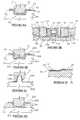
- a substratecomprises a semiconductor wafer 10 W containing a plurality of components in the form of semiconductor dice 11 D.
- the semiconductor wafer 10 Wcomprises a semiconducting material such as silicon or gallium arsenide.
- FIG. 1Billustrates a die 11 D that has been separated from the wafer 10 W.
- the die 11 Dincludes an array of bumped component contacts 12 D, such as solder balls, formed on a face thereof.
- the bumped component contacts 12 Dare formed in a pattern P 1 , such as a dense ball grid array (BGA).
- BGAdense ball grid array
- the bumped component contacts 12 Dare bonded to planar bond pads 13 D on the die 11 D in electrical communication with the integrated circuits contained on the die 11 D.
- the bond pads 13 Dare surrounded by a die passivation layer 14 D formed on the face of the die 11 D.
- solder fillets 15 Dattach the bumped component contacts 12 D to the bond pads 13 D.
- a substratecomprises a panel 10 P containing a plurality of semiconductor components in the form of chip scale packages 11 CSP.
- the panel 10 Pcomprises an electrically insulating material such as ceramic, a reinforced polymer laminate, such as bismaleimide triazine (BT), or an epoxy resin (e.g., FR-4).
- BTbismaleimide triazine
- FR-4epoxy resin
- each chip scale package 11 CSPincludes a substrate 10 CSP.
- the substrate 10 CSPcomprises a segment of the panel 10 P which has been cut, sheared, punched or otherwise separated from a remainder of the panel 10 P.
- each chip scale package 11 CSPincludes a semiconductor die 17 CSP wire bonded to the substrate 10 CSP, an adhesive layer 19 CSP which attaches the die 17 CSP to the substrate 10 CSP, and an encapsulating resin 21 CSP encapsulating the die 17 CSP.
- Each chip scale package 11 CSPalso includes an array of bumped component contacts 12 CSP in electrical communication with the integrated circuits contained on the die 17 CSP.
- the bumped component contacts 12 CSPare formed on the substrate 10 CSP in a dense grid array, such as a ball grid array (BGA), or a fine ball grid array (FBGA).
- a representative diameter D 1 for the bumped component contacts 12 CSPcan be about 0.005-in (0.127 mm) to 0.050-in (1.270 mm) or greater.
- a representative pitch P (center to center spacing) of the bumped component contacts 12 CSPcan be from about 0.008-in (0.228 mm) to about 0.060-in (1.524 mm) or greater.
- a test system 16 constructed in accordance with the invention, and configured to test components 11 contained on a substrate 10is illustrated.
- a single component 11is illustrated on the substrate 10 .
- the substrate 10will contain multiple components 11 , similarly to the wafer 10 W (FIG. 1 A), or the panel 10 P (FIG. 2 A), previously described.
- the components 11 on the substrate 10include patterns of bumped component contacts 12 in electrical communication with integrated circuits and other electrical elements on the components 11 .
- the test system 16includes a test head 30 and an interconnect 20 .
- the interconnect 20includes patterns of interconnect contacts 22 configured to make temporary electrical connections with the bumped component contacts 12 .
- the test system 16also includes a wafer prober 18 wherein the interconnect 20 is mounted, and a tester 26 configured to apply test signals through the interconnect 20 , to the components 11 contained on the substrate 10 , and to analyze the resultant signals.
- the wafer prober 18includes an interconnect holder 62 for mounting and electrically interfacing with the interconnect 20 . Further details of mounting the interconnect 20 to the test head 30 will be hereinafter described.
- the wafer prober 18also includes a wafer chuck 24 configured to move in X and Y directions to align the substrate 10 with the interconnect 20 , and in the Z direction to move the substrate 10 into contact with the interconnect 20 .
- a wafer chuck 24configured to move in X and Y directions to align the substrate 10 with the interconnect 20 , and in the Z direction to move the substrate 10 into contact with the interconnect 20 .
- One suitable wafer prober 18is manufactured by Electroglass and is designated a Model 4080.
- the test system 16also includes a prober interface board 28 for routing test signals from the test head 30 to the interconnect 20 .
- the prober interface board 28can be in electrical communication with tester pin electronics 32 in the test head 30 .
- the tester pin electronics 32provide separate electrical paths 34 from test circuitry 33 contained in the tester 26 , to the test head 30 and to the prober interface board 28 .
- tester resourcesThe signal generating and analyzing capability of the test circuitry 33 , and the number of separate electrical paths 34 provided by the tester pin electronics 32 , are termed herein as “tester resources”.
- the configurations of the test circuitry 33 , and of the electrical paths 34are fixed for a particular tester 26 by the manufacturer.
- the test circuitry 33can be configured to route drive only signals through some of the electrical paths 34 , and input/output channels through other of the electrical paths 34 , as required for testing a particular type of die 12 .
- Exemplary testers 26are commercially available from Teradyne of Boston, Mass., as well as other manufacturers.
- the interconnect contacts 22are arranged in patterns corresponding to the patterns of the bumped component contacts 12 .
- Each pattern of interconnect contacts 22represents a single test site (S).
- Stest site
- the interconnect 20can include multiple patterns of interconnect contacts 22 forming multiple test sites (S 1 . . . Sn) to accommodate testing of multiple components 11 at the same time.
- the patterns of interconnect contacts 22must exactly match the patterns of the bumped component contacts 12 .
- the stepping distancei.e., x-y repeat and pattern spacing
- the software that controls the stepping processmust be able to pick valid test sites. For example, when testing at the edges of a round wafer with an interconnect that includes rectangular or square patterns of interconnect contacts 22 , some patterns of interconnect contacts 22 will not have an associated component under test.
- the use of the interconnect 20can greatly reduce the number of steps necessary for the prober 18 to test all of the components 11 contained on the substrate 10 .
- the interconnect 20can be formed with enough patterns of interconnect contacts 22 to simultaneously contact every bumped component contact 12 for all of the components 11 on the substrate 10 . Test signals can then be selectively applied and electronically switched as required, to selected components 11 on the substrate 10 .
- the interconnect 20can be formed with any desired number of test sites (S 1 . . . Sn).
- the interconnect 20in addition to the patterns of interconnect contacts 22 , the interconnect 20 includes patterns of conductors 36 in electrical communication with the interconnect contacts 22 and with on-board circuitry 38 .
- the interconnect contacts 22 and conductors 36are formed on a substrate 40 of the interconnect 20 .
- the interconnect substrate 40comprises silicon (or another semiconducting material such as gallium arsenide). This permits the on-board circuitry 38 to be formed as integrated circuits on the interconnect substrate 40 using semiconductor circuit fabrication techniques such as doping, CVD, photolithography, and etching. Also, with the interconnect substrate 40 comprising silicon, a coefficient of thermal expansion of the interconnect 20 exactly matches that of the substrate 10 .
- the interconnect substrate 40can also comprise a silicon containing material, such as silicon-on-glass, and the on board circuitry can be formed on a layer of the interconnect substrate 40 .
- the interconnect substrate 40is thick enough to resist deflection and buckling during test procedures using the interconnect 20 .
- an electrically insulating layer 42such as SiO 2 , polyimide, or BPSG can be formed on the substrate 40 to provide insulation for the interconnect contacts 22 and conductors 36 from the bulk of the interconnect substrate 40 .
- the conductors 36 on the substrate 40are in electrical communication with the interconnect contacts 22 , and with the on board circuitry 38 .
- the conductors 36can be formed on a surface of the substrate 40 in a required pattern.
- the conductors 36can include interlevel segments, such as metal vias or other interlevel electrical paths, that are in electrical communication with other components of the on-board circuitry 38 .
- the conductors 36can be placed in electrical communication with the test circuitry 33 (FIG. 3) to provide electrical paths from the test circuitry 33 to the on-board circuitry 38 , and to the interconnect contacts 22 .
- the conductors 36comprise a highly conductive metal such as copper, aluminum, titanium, tantalum, tungsten, molybdenum or alloys of these metals.
- the conductors 36can be formed as a single layer of metal, or as a multi metal stack, using a thin film metallization process (e.g., CVD, patterning, etching). Alternately, a thick film metallization process (e.g., screen printing, stenciling) can be used to form the conductors 36 .
- the conductors 36also include bonding pads 44 located along the peripheral edges of the interconnect 20 .
- the bonding pads 44provide bonding sites for forming separate electrical paths from the interconnect holder 62 (FIG. 1) to each of the conductors 36 .
- the bonding pads 44are located on recessed surfaces 46 (FIG. 5F) along the edges of the interconnect substrate 40 to provide clearance for TAB bonds, wire bonds, spring loaded connectors (e.g., “POGO PINS”) or other electrical connections to the bonding pads 44 .
- the interconnect contact 22includes a conductive pocket 50 formed in the interconnect substrate 40 , and a conductive layer 52 formed on the pocket 50 .
- the pocket 50can be etched by forming a mask (not shown) on the interconnect substrate 40 , such as a photopatterned resist mask, and then etching the interconnect substrate 40 through openings in the mask, using an etchant.
- a suitable etchant for performing the etch processcomprises a solution of KOH.
- a size and shape of the pocket 50will be determined by the openings in the etch mask used to etch the interconnect substrate 40 .
- the pocket 50is sized and shaped to retain and electrically engage the bumped component contact 12 .
- a representative diameter, or width, of the pocket 50can be from 2 mils to 50 mils or more. This diameter can be less than a diameter of the bumped component contact 12 so that only portions of the bumped component contact 12 will be contacted.
- a depth of the pocket 50can be equal to or less than the diameter of the pocket 50 .
- a pitch or spacing of the pocket 50 relative to adjacent pockets 50 on the interconnect 20will exactly match a pitch or spacing of the component contacts 12 on the component 11 .
- the conductive layer 52can comprise a layer of a highly conductive metal such as aluminum, titanium, nickel, iridium, copper, gold, tungsten, silver, platinum, palladium, tantalum, molybdenum or alloys of these metals.
- the conductive layer 52can be formed on the insulating layer 42 to a desired thickness using a suitable metallization process (e.g., CVD, photopatterning, etching). Peripheral edges 54 of the conductive layer 52 are adapted to penetrate native oxide layers on the bumped component contacts 12 to contact the underlying metal.
- the conductive layer 52is in electrical communication with a selected conductor 36 (FIG. 4 ).
- the conductive layer 52 and selected conductor 36can be formed using a same metallization process or using different metalization processes.
- the conductive layer 52 and conductor 36can be formed as multi-layered stacks of metals (e.g., bonding layer/barrier layer).
- the conductor 36can be electrically insulated with an outer insulating layer (not shown).
- the interconnect contact 22 Aincludes a pocket 50 A formed in a substrate 40 A.
- the interconnect contact 22 Aincludes an insulating layer 42 A, and a conductive layer 52 A. Each of these elements are substantially similar to the previously described elements of interconnect contact 22 (FIG. 5 A).
- the interconnect contact 22 Aalso includes a penetrating blade 56 configured to penetrate into the bumped component contact 12 to form a reliable electrical connection therewith. Further details of the interconnect contact 22 A are described in previously cited U.S. patent application Ser. No. 08/829,193.
- a third embodiment interconnect contact 22 Bcomprises a projection formed integrally with a substrate 40 B, which preferably comprises silicon or other etchable material.
- a substrate 40 Bwhich preferably comprises silicon or other etchable material.
- One method for forming the interconnect contact 22 Bis by etching the substrate 40 B as described in U.S. Pat. No. 5,483,741, entitled “METHOD FOR FABRICATING A SELF LIMITING SILICON BASED INTERCONNECT FOR TESTING BARE SEMICONDUCTOR DICE”, which is incorporated herein by reference.
- the interconnect contact 22 Bincludes a conductive layer 52 B formed using a metallization process as previously described.
- the conductive layer 52 Bis in electrical communication with a selected conductor 36 on the substrate 40 B.
- an insulating layer 42 Bcan be formed on the substrate 40 B to electrically insulate the conductive layer 52 B from the bulk of the substrate 40 B.
- the interconnect contact 22 Bis adapted to penetrate into the bumped component contact 12 to form an electrical connection therewith.
- the interconnect contact 22 Bis shown as penetrating a center of the bumped component contact 12 , forming a void in the bumped component contact 12 .
- penetrationcan be along the peripheral edges of the bumped component contact 12 in which case a groove would be formed.
- a fourth embodiment interconnect contact 22 Bcomprises a pocket 50 C covered with a conductive layer 52 C in electrical communication with a selected conductor 36 , substantially as previously described.
- the pocket 50 Cis formed on an elastomeric layer 58 formed on a substrate 40 C.
- the elastomeric layer 58comprises a compliant polymer material that allows the interconnect contact 22 B to move in the z-direction to accommodate variations in the size, location, and planarity in the bumped component contacts 12 .
- Suitable materials for the elastomeric layer 58include polyimide, photoimageable polyimide, polyester, epoxy, urethane, polystyrene, silicone and polycarbonate. These materials can be cast in place to a desired thickness using known processes such as spin on, or dispensing through a nozzle. Alternately, these materials can be in the form of a tape, such as “KAPTON” tape, which can be applied to the substrate 40 C using an adhesive layer.
- a representative thickness for the elastomeric layer 58can be from 0.5 ⁇ m to 50 ⁇ m.
- FIG. 5Ean enlarged cross sectional view of a FET transistor 100 of the on board circuitry 38 (FIG. 4) is illustrated.
- the FET transistor 100is merely one component of the on board circuitry 38 .
- the on board circuitry 38can include many FET transistors 100 , as well as additional components, to provide the circuit arrangements that will be hereinafter explained. Further, other active electrical switching devices, such as NPN or PNP transistors can be used in place of the FET transistor 100 illustrated in the preferred embodiment.
- the FET transistors 100can be formed integrally with the substrate 40 using semiconductor circuit fabrication techniques.
- a suitable process sequencecan include initially etching the interconnect contacts 22 (FIG. 5A) and then fabricating the FET transistors 100 .
- the insulating layer 42can be formed, the conductive layers 52 (FIG. 5A) can be formed, and the conductors 36 (FIG. 4) can be formed.
- Each FET transistor 100includes a polysilicon gate 102 , and a gate oxide 104 .
- a field oxide 106is formed on the substrate 40 for electrically isolating the FET transistors 100 .
- the substrate 40also includes N+ active areas 108 , which can be formed by implanting dopants into the substrate 40 to form the sources and drains of the FET transistors 100 .
- Metal filled vias 110 with metal silicide layers 112electrically connect the sources and drains of the FET transistors 100 to the conductors 36 .
- the FET transistors 100also include spacers 114 , TEOS layers 116 and nitride caps 118 .
- interconnect 20 Ais illustrated.
- the interconnect 20 Ais substantially similar to the interconnect 20 previously described, but includes on board circuitry 38 A formed on a die 48 mounted to a substrate 40 D rather than being formed integrally therewith.
- the substrate 40can comprise silicon, ceramic, or a glass filled resin (FR-4).
- the die 48is flip chip mounted to the substrate 40 D in electrical communication with the interconnect contacts 22 .
- the die 48includes bumped bond pads 60 .
- the interconnect substrate 40 Dincludes interconnect contacts 22 D configured to physically and electrically engage the bumped bond pads 60 .
- the interconnect contacts 22 Dcan be formed substantially as previously described for interconnect contacts 22 (FIG. 5 A).
- the interconnect contacts 22 Dare in electrical communication with selected conductors 36 (FIG. 4A) on the substrate 40 D.
- the bumped bond pads 60can be bonded to the interconnect contacts 22 D using a bonding process such as solder reflow, or by heating opposing metal surfaces.
- the die 48can be mechanically bonded to the substrate 40 D using an encapsulant or a mechanical fixture. Further, the die 48 can be located on the substrate 40 D such that the interconnect contacts 22 (FIG. 4A) electrically engage the bumped component contacts 12 (FIG. 5A) without interference from the die 48 .
- an alternate embodiment interconnect 20 Bis attached to an interposer 84 B, which includes on-board circuitry 38 B, substantially as previously described.
- the interposer 84 Bcan comprise a semiconducting material such as silicon, in which case the on-board circuitry 38 B can be fabricated on the interposer 84 B using semiconductor circuit fabrication techniques. Wires 88 can then be bonded to pads on the interconnect 20 B and to pads on the interposer 84 A to provide separate electrical paths therebetween.
- an alternate embodiment interconnect 20 Cincludes on-board circuitry 38 C contained on a die 86 attached to an interposer 84 C (or directly to the interconnect 20 C).
- the die 86is flip chip mounted to the interposer 84 C. Reflowed solder bumps 90 on the die 86 are bonded to internal conductors 92 on the interposer 84 C.
- the internal conductors 92are in electrical communication with the interconnect contacts 22 on the interconnect 20 C.
- the wafer prober 18includes the interconnect holder 62 , a force applying fixture 64 and a force applying mechanism 66 . These items can be components of a conventional wafer prober as previously described.
- the force applying mechanism 66presses against a pressure plate 68 and a compressible member 70 to bias the interconnect 20 against the substrate 10 .
- the compressible member 70can be formed of an elastomeric material such as silicone, butyl rubber, or fluorosilicone; in foam, gel, solid or molded configurations.
- a flexible membrane 72is bonded to the interconnect 20 and to the interconnect holder 62 .
- the flexible membrane 72functions to physically attach the interconnect 20 to the interconnect holder 62 .
- the flexible membrane 72functions to provide electrical paths between the interconnect contacts 22 and the test circuitry 33 (FIG. 3) of the tester 26 .
- the flexible membrane 72can be formed of thin flexible materials to allow movement of the interconnect 20 in Z-directions.
- the flexible membrane 72can be formed of a flexible multi layered material similar to TAB tape.
- the flexible membrane 72comprises a layer of polymer tape having metal conductors thereon. Bonded connections are formed between the conductors on the membrane 72 and corresponding conductors 74 on the interconnect holder 62 . In addition, bonded connections are formed between the conductors on the membrane 72 and the bonding pads 44 on the interconnect 20 .
- the wafer prober 18includes spring loaded electrical connectors 76 which are in electrical communication with the prober interface board 28 .
- spring loaded electrical connector 76is manufactured by Pogo Industries of Kansas City, Mo. under the trademark “POGO PINS”.
- the electrical connectors 76electrically communicate with the conductors 74 on the interconnect holder 62 .
- steps in a method for testing the substrate 10 using the test system 18 and interconnect 20are illustrated. These steps are as follows.
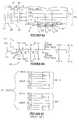
- FIGS. 8A-8Dfurther details of the on board circuitry 38 (FIG. 4) are illustrated.
- a single test site Sis illustrated.
- the test site S on the interconnect 20includes a pattern of interconnect contacts 22 which are configured to electrically engage bumped component contacts 12 on the component 11 being tested, which is termed the “device under test” (DUT).
- DUTdevice under test
- the interconnect 20is in electrical communication with the interconnect holder 62 , the tester pin electronics 32 , and the test circuitry 33 within the tester 26 .
- the on board circuitry 38includes a multiplex circuit 80 .
- the multiplex circuit 80is configured to receive test signals from the test circuitry 33 and to fan out or multiply the test signals.
- the multiplex circuit 80is configured to selectively address the fanned out test signals through the interconnect contacts 22 to selected bumped component contacts 12 on the DUT. Stated differently, the multiplex circuit permits the test signals to be fanned out, allowing test procedures to be conducted in parallel.
- the multiplex circuit 80is configured to maintain the uniqueness of individual DUTs, and to electrically disconnect defective DUTs as required.
- the multiplex circuit 80includes a Util channel for each DUT, which functions as a control channel.
- the multiplex circuit 80includes drive only channels, Vs channels, and I/O channels. The numbers of the channels are determined by the tester resources. Table I lists the tester resources of a Model “J993” tester 26 manufactured by Teradyne.
- Table IIlists the tester resources of a Model “J994” tester 26 manufactured by Teradyne.
- Table IIIlists the test requirements for one type of SRAM.
- I/O channels per DUT 18address channels (drive only) per DUT 32 control channels (drive only) per DUT 6 power supply channels (Vs-voltage supplies) per DUT Util channels used depends on parallelism Total 36 I/O channels per DUT 50 drive only channels per DUT 6 Vs channels per DUT
- a “J993” tester 26can test two DUTs per test head 30 , due to the I/O requirements. This is shown schematically in FIG. 8 C.
- the (J993) tester 26includes a first test head 30 - 0 and a second test head 30 - 1 .
- Each test head 30 - 0 , 30 - 1is capable of testing two DUTs, for a total of four at a time.
- both substrates 10one on each test head
- a “J994” tester 26has twice the tester resources of a “J993” tester 26 . Accordingly, on the basis of the above sample I/O requirements, a “J994” tester 26 can test four DUTs per test head 30 , for a total of eight at a time.
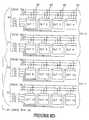
- the multiplex circuit 80simply stated, comprises multiple FET transistors 100 configured to provide a switching circuit for selectively enabling and disabling the interconnect contacts 22 .
- the gate 102 of each FET transistor 100is in electrical communication with the Util 0 channel.
- a controller 120(or computer) generates control signals which are transmitted through the Util 0 channel to the FET transistors 100 .
- the multiplex circuit 80is configured to test the SRAM of Table III. Accordingly, there are six Vs channels (Vs 0 . . . Vs 5 ), eighteen address channels (A 0 . . . A 17 ), and thirty six I/O channels (I/O 0 -I/O 35 ). In addition, there is an OE channel, a CE channel, and an “all other controls” channel. With this arrangement test signals can be transmitted from the test circuitry 33 and latched by the channels. Control signals from the controller 120 then control the FET transistors 100 to enable and disable the contacts 22 to selectively transmit the test signals to the bumped component contacts 12 as required.
- control signalscan be used to operate the FET transistors 100 to disable selected contacts 22 in order to electrically disconnect defective DUTs. Still further, the control signals can be used to operate the FET transistors 100 to enable and disable selected contacts 22 in the transmission of “read” signals from the DUTs. However, in the “read” mode the DUTs must be read in accordance with the tester resources.
- the multiplex circuit 80 illustrated in FIG. 8Bis merely exemplary. Those skilled in the art, with the aid of the present specification, can design other multiplex circuits able to multiply and selectively address test signals from a tester. Thus other types of multiplexing circuits are intended to be included within the scope of the present claims.
- each test sitecan write test signals to four DUTs at a time.
- the additional three DUTs per test sitemust be selected in accordance with tester resources (e.g., one at a time or two at a time).
- a limiting factor in the number of DUTs that can be tested by each test siteis the drive current capacity of the channels of the tester 26 .
- the drive current capacityis about 50 mA per channel.
- the test signalscan be specified with a current (IOL) of about 8 mA per channel.
- IOLcurrent
- each I/O channel and drive only channel of the tester 26can be configured to drive four DUTs substantially as shown in FIG. 8 D.
- there is 8 mA per DUT ⁇ 4 DUTs32 mA per tester drive only channel. This leaves a 18 mA per channel margin.
- the inventionprovides an improved interconnect for testing semiconductor components contained on a substrate, a method for testing semiconductor components using the interconnect, and a test system employing the interconnect.
- the interconnectcan include interconnect contacts in dense arrays to accommodate testing of multiple components having dense arrays of component contacts.
- the interconnectincludes on board circuitry configured to expand tester resources.
Landscapes
- Physics & Mathematics (AREA)
- General Physics & Mathematics (AREA)
- Testing Or Measuring Of Semiconductors Or The Like (AREA)
Abstract
Description
| TABLE I |
| Tester Resources of Teradyne “J993” |
| 16 power supply channels per test head (30) | ||
| 16X, 16Y address generation channels per test head (30) | ||
| 16 DUTs can be tested in parallel per test head (30) | ||
| 72 I/O channels per test head (30) | ||
| 2 heads (30) per tester (26) | ||
| 320 drive only channels per head (30) divisible as | ||
| follows: | ||
| 80 per test site (S) with 4 test sites (S0-S3) | ||
| 40 per test site (S) with 8 test sites (S0-S7) | ||
| 20 per test site (S) with 16 test sites (S0-S15) | ||
| Up to 320 megabits of | ||
| 36 Util channels per test head (30) | ||
| TABLE II |
| Tester Resources of Teradyne “J994” |
| 32 power supply channels per test head (30) | ||
| 16X, 16Y address generation channels per test head (30) | ||
| 32 DUTs can be tested in parallel per test head (30) | ||
| 144 I/O channels per test head (30) | ||
| 2 heads (30) per tester (26) | ||
| 640 drive only channels per | ||
| follows: | ||
| 80 per test site (S) with 8 test sites (S1-S8) | ||
| 40 per test site (S) with 16 test sites (S1-S16) | ||
| 20 per test site (S) with 32 test sites (S1-S32) | ||
| Up to 640 megabits of | ||
| 52 Util channels per test head (30) | ||
| TABLE III |
| Sample SRAM Requirements For Each Device Under Test DUT |
| 36 I/O channels per | ||
| 18 address channels (drive only) per | ||
| 32 control channels (drive only) per | ||
| 6 power supply channels (Vs-voltage supplies) per DUT | ||
| Util channels used depends on parallelism | ||
| Total | ||
| 36 I/O channels per | ||
| 50 drive only channels per | ||
| 6 Vs channels per DUT | ||
Claims (26)
Priority Applications (2)
| Application Number | Priority Date | Filing Date | Title |
|---|---|---|---|
| US09/999,502US6466047B1 (en) | 1998-05-11 | 2001-12-04 | System for testing bumped semiconductor components with on-board multiplex circuit for expanding tester resources |
| US10/223,826US6677776B2 (en) | 1998-05-11 | 2002-08-20 | Method and system having switching network for testing semiconductor components on a substrate |
Applications Claiming Priority (4)
| Application Number | Priority Date | Filing Date | Title |
|---|---|---|---|
| US09/075,691US6246250B1 (en) | 1998-05-11 | 1998-05-11 | Probe card having on-board multiplex circuitry for expanding tester resources |
| US09/244,373US6337577B1 (en) | 1998-05-11 | 1999-02-04 | Interconnect and system for testing bumped semiconductor components with on-board multiplex circuitry for expanding tester resources |
| US09/675,072US6433574B1 (en) | 1998-05-11 | 2000-09-28 | Interconnect and system for testing bumped semiconductor components with on-board multiplex circuitry for expanding tester resources |
| US09/999,502US6466047B1 (en) | 1998-05-11 | 2001-12-04 | System for testing bumped semiconductor components with on-board multiplex circuit for expanding tester resources |
Related Parent Applications (1)
| Application Number | Title | Priority Date | Filing Date |
|---|---|---|---|
| US09/675,072DivisionUS6433574B1 (en) | 1998-05-11 | 2000-09-28 | Interconnect and system for testing bumped semiconductor components with on-board multiplex circuitry for expanding tester resources |
Related Child Applications (1)
| Application Number | Title | Priority Date | Filing Date |
|---|---|---|---|
| US10/223,826Continuation-In-PartUS6677776B2 (en) | 1998-05-11 | 2002-08-20 | Method and system having switching network for testing semiconductor components on a substrate |
Publications (1)
| Publication Number | Publication Date |
|---|---|
| US6466047B1true US6466047B1 (en) | 2002-10-15 |
Family
ID=26757166
Family Applications (3)
| Application Number | Title | Priority Date | Filing Date |
|---|---|---|---|
| US09/244,373Expired - Fee RelatedUS6337577B1 (en) | 1998-05-11 | 1999-02-04 | Interconnect and system for testing bumped semiconductor components with on-board multiplex circuitry for expanding tester resources |
| US09/675,072Expired - LifetimeUS6433574B1 (en) | 1998-05-11 | 2000-09-28 | Interconnect and system for testing bumped semiconductor components with on-board multiplex circuitry for expanding tester resources |
| US09/999,502Expired - LifetimeUS6466047B1 (en) | 1998-05-11 | 2001-12-04 | System for testing bumped semiconductor components with on-board multiplex circuit for expanding tester resources |
Family Applications Before (2)
| Application Number | Title | Priority Date | Filing Date |
|---|---|---|---|
| US09/244,373Expired - Fee RelatedUS6337577B1 (en) | 1998-05-11 | 1999-02-04 | Interconnect and system for testing bumped semiconductor components with on-board multiplex circuitry for expanding tester resources |
| US09/675,072Expired - LifetimeUS6433574B1 (en) | 1998-05-11 | 2000-09-28 | Interconnect and system for testing bumped semiconductor components with on-board multiplex circuitry for expanding tester resources |
Country Status (1)
| Country | Link |
|---|---|
| US (3) | US6337577B1 (en) |
Cited By (10)
| Publication number | Priority date | Publication date | Assignee | Title |
|---|---|---|---|---|
| EP1371995A1 (en)* | 2003-04-10 | 2003-12-17 | Agilent Technologies, Inc. | Serial communication testing |
| US20030235929A1 (en)* | 2002-06-20 | 2003-12-25 | Micron Technology, Inc. | Signal sharing circuit with microelectronic die isolation features |
| US20030234393A1 (en)* | 2002-06-20 | 2003-12-25 | Micron Technology, Inc. | Isolation circuit |
| US6677776B2 (en)* | 1998-05-11 | 2004-01-13 | Micron Technology, Inc. | Method and system having switching network for testing semiconductor components on a substrate |
| US20060158203A1 (en)* | 2005-01-14 | 2006-07-20 | Volkerink Erik H | Allocating device testing resources |
| US20080106279A1 (en)* | 2006-11-03 | 2008-05-08 | Micron Technology Inc. | Probe card layout |
| US20100264951A1 (en)* | 2008-04-21 | 2010-10-21 | Fujitsu Limited | Interconnection card for inspection, manufacture method for interconnection card, and inspection method using interconnection card |
| US20100295567A1 (en)* | 2009-05-19 | 2010-11-25 | Hsi-Ming Chang | Resistance measuring device, display panel, and measuring method of bonding resistance |
| US20110121848A1 (en)* | 2008-03-26 | 2011-05-26 | Advantest Corporation | Probe wafer, probe device, and testing system |
| US20220085261A1 (en)* | 2020-09-17 | 2022-03-17 | Samsung Display Co., Ltd. | Display device |
Families Citing this family (25)
| Publication number | Priority date | Publication date | Assignee | Title |
|---|---|---|---|---|
| US5894161A (en)* | 1997-02-24 | 1999-04-13 | Micron Technology, Inc. | Interconnect with pressure sensing mechanism for testing semiconductor wafers |
| US6980017B1 (en) | 1999-03-10 | 2005-12-27 | Micron Technology, Inc. | Test interconnect for bumped semiconductor components and method of fabrication |
| US6437591B1 (en) | 1999-03-25 | 2002-08-20 | Micron Technology, Inc. | Test interconnect for bumped semiconductor components and method of fabrication |
| US6380555B1 (en)* | 1999-12-24 | 2002-04-30 | Micron Technology, Inc. | Bumped semiconductor component having test pads, and method and system for testing bumped semiconductor components |
| US6605951B1 (en)* | 2000-12-11 | 2003-08-12 | Lsi Logic Corporation | Interconnector and method of connecting probes to a die for functional analysis |
| US7174490B2 (en)* | 2002-04-12 | 2007-02-06 | Broadcom Corporation | Test system rider utilized for automated at-speed testing of high serial pin count multiple gigabit per second devices |
| US7363557B2 (en)* | 2002-04-12 | 2008-04-22 | Broadcom Corporation | System for at-speed automated testing of high serial pin count multiple gigabit per second devices |
| US7278079B2 (en)* | 2002-04-12 | 2007-10-02 | Broadcom Corporation | Test head utilized in a test system to perform automated at-speed testing of multiple gigabit per second high serial pin count devices |
| US7502326B2 (en)* | 2002-04-12 | 2009-03-10 | Broadcom Corporation | Methods used to simultaneously perform automated at-speed testing of multiple gigabit per second high serial pin count devices |
| DE60306008T2 (en)* | 2002-04-12 | 2007-01-11 | Broadcom Corp., Irvine | Devices and methods for high-speed testing of high pin count, multi-gigabit circuits |
| US6768331B2 (en) | 2002-04-16 | 2004-07-27 | Teradyne, Inc. | Wafer-level contactor |
| US6720195B2 (en) | 2002-05-15 | 2004-04-13 | Micron Technology, Inc. | Methods employing elevated temperatures to enhance quality control in microelectronic component manufacture |
| US7127652B2 (en)* | 2003-06-03 | 2006-10-24 | Agilent Technologies, Inc. | X-tree test method and apparatus in a multiplexed digital system |
| US7319341B1 (en)* | 2003-08-28 | 2008-01-15 | Altera Corporation | Method of maintaining signal integrity across a capacitive coupled solder bump |
| US7030632B2 (en)* | 2003-10-14 | 2006-04-18 | Micron Technology, Inc. | Compliant contract structures, contactor cards and test system including same |
| JP2005183863A (en)* | 2003-12-24 | 2005-07-07 | Renesas Technology Corp | Method for manufacturing semiconductor integrated circuit device |
| US7262615B2 (en)* | 2005-10-31 | 2007-08-28 | Freescale Semiconductor, Inc. | Method and apparatus for testing a semiconductor structure having top-side and bottom-side connections |
| JP5351151B2 (en)* | 2008-05-28 | 2013-11-27 | 株式会社アドバンテスト | Test system |
| WO2010104913A1 (en) | 2009-03-10 | 2010-09-16 | Johnstech International | Electrically conductive pins for microcircuit tester |
| US20130002285A1 (en) | 2010-03-10 | 2013-01-03 | Johnstech International Corporation | Electrically Conductive Pins For Microcircuit Tester |
| TWI534432B (en) | 2010-09-07 | 2016-05-21 | 瓊斯科技國際公司 | Electrical conduction pins for microcircuit testers |
| US9007082B2 (en) | 2010-09-07 | 2015-04-14 | Johnstech International Corporation | Electrically conductive pins for microcircuit tester |
| CN102081111A (en)* | 2010-12-06 | 2011-06-01 | 上海华岭集成电路技术股份有限公司 | Probe card |
| US9316685B2 (en)* | 2012-11-12 | 2016-04-19 | Mpi Corporation | Probe card of low power loss |
| US10930535B2 (en)* | 2016-12-02 | 2021-02-23 | Applied Materials, Inc. | RFID part authentication and tracking of processing components |
Citations (49)
| Publication number | Priority date | Publication date | Assignee | Title |
|---|---|---|---|---|
| US3806801A (en) | 1972-12-26 | 1974-04-23 | Ibm | Probe contactor having buckling beam probes |
| US4027935A (en) | 1976-06-21 | 1977-06-07 | International Business Machines Corporation | Contact for an electrical contactor assembly |
| US4585991A (en) | 1982-06-03 | 1986-04-29 | Texas Instruments Incorporated | Solid state multiprobe testing apparatus |
| US4891585A (en) | 1986-09-05 | 1990-01-02 | Tektronix, Inc. | Multiple lead probe for integrated circuits in wafer form |
| US4906920A (en) | 1988-10-11 | 1990-03-06 | Hewlett-Packard Company | Self-leveling membrane probe |
| US4918383A (en) | 1987-01-20 | 1990-04-17 | Huff Richard E | Membrane probe with automatic contact scrub action |
| US4954458A (en) | 1982-06-03 | 1990-09-04 | Texas Instruments Incorporated | Method of forming a three dimensional integrated circuit structure |
| US5042148A (en) | 1989-10-11 | 1991-08-27 | Mitsubishi Denki Kabushiki Kaisha | Method of manufacturing a probing card for wafer testing |
| US5053700A (en) | 1989-02-14 | 1991-10-01 | Amber Engineering, Inc. | Method for wafer scale testing of redundant integrated circuit dies |
| US5055780A (en) | 1989-03-09 | 1991-10-08 | Mitsubishi Denki Kabushiki Kaisha | Probe plate used for testing a semiconductor device, and a test apparatus therefor |
| US5070297A (en) | 1990-06-04 | 1991-12-03 | Texas Instruments Incorporated | Full wafer integrated circuit testing device |
| US5103557A (en) | 1988-05-16 | 1992-04-14 | Leedy Glenn J | Making and testing an integrated circuit using high density probe points |
| US5124639A (en) | 1990-11-20 | 1992-06-23 | Motorola, Inc. | Probe card apparatus having a heating element and process for using the same |
| US5172050A (en) | 1991-02-15 | 1992-12-15 | Motorola, Inc. | Micromachined semiconductor probe card |
| US5177439A (en) | 1991-08-30 | 1993-01-05 | U.S. Philips Corporation | Probe card for testing unencapsulated semiconductor devices |
| US5180977A (en) | 1991-12-02 | 1993-01-19 | Hoya Corporation Usa | Membrane probe contact bump compliancy system |
| US5196726A (en) | 1990-01-23 | 1993-03-23 | Sumitomo Electric Industries, Ltd. | Substrate for packaging a semiconductor device having particular terminal and bump structure |
| US5225037A (en) | 1991-06-04 | 1993-07-06 | Texas Instruments Incorporated | Method for fabrication of probe card for testing of semiconductor devices |
| US5264787A (en) | 1991-08-30 | 1993-11-23 | Hughes Aircraft Company | Rigid-flex circuits with raised features as IC test probes |
| US5323107A (en) | 1991-04-15 | 1994-06-21 | Hitachi America, Ltd. | Active probe card |
| US5329423A (en) | 1993-04-13 | 1994-07-12 | Scholz Kenneth D | Compressive bump-and-socket interconnection scheme for integrated circuits |
| US5475317A (en) | 1993-12-23 | 1995-12-12 | Epi Technologies, Inc. | Singulated bare die tester and method of performing forced temperature electrical tests and burn-in |
| US5477160A (en) | 1992-08-12 | 1995-12-19 | Fujitsu Limited | Module test card |
| US5483741A (en) | 1993-09-03 | 1996-01-16 | Micron Technology, Inc. | Method for fabricating a self limiting silicon based interconnect for testing bare semiconductor dice |
| US5491427A (en) | 1993-08-21 | 1996-02-13 | Hewlett-Packard Company | Probe and electrical part/circuit inspecting apparatus as well as electrical part/circuit inspecting method |
| US5500605A (en) | 1993-09-17 | 1996-03-19 | At&T Corp. | Electrical test apparatus and method |
| US5592736A (en) | 1993-09-03 | 1997-01-14 | Micron Technology, Inc. | Fabricating an interconnect for testing unpackaged semiconductor dice having raised bond pads |
| US5625298A (en) | 1993-09-30 | 1997-04-29 | International Business Machines Corp. | Semi-conductor chip test probe |
| US5686317A (en) | 1991-06-04 | 1997-11-11 | Micron Technology, Inc. | Method for forming an interconnect having a penetration limited contact structure for establishing a temporary electrical connection with a semiconductor die |
| US5736850A (en) | 1995-09-11 | 1998-04-07 | Teradyne, Inc. | Configurable probe card for automatic test equipment |
| US5789271A (en) | 1996-03-18 | 1998-08-04 | Micron Technology, Inc. | Method for fabricating microbump interconnect for bare semiconductor dice |
| US5834945A (en) | 1996-12-31 | 1998-11-10 | Micron Technology, Inc. | High speed temporary package and interconnect for testing semiconductor dice and method of fabrication |
| US5869974A (en) | 1996-04-01 | 1999-02-09 | Micron Technology, Inc. | Micromachined probe card having compliant contact members for testing semiconductor wafers |
| US5915977A (en) | 1997-06-02 | 1999-06-29 | Micron Technology, Inc. | System and interconnect for making temporary electrical connections with bumped semiconductor components |
| US5962921A (en) | 1997-03-31 | 1999-10-05 | Micron Technology, Inc. | Interconnect having recessed contact members with penetrating blades for testing semiconductor dice and packages with contact bumps |
| US6016060A (en) | 1997-03-25 | 2000-01-18 | Micron Technology, Inc. | Method, apparatus and system for testing bumped semiconductor components |
| US6040702A (en) | 1997-07-03 | 2000-03-21 | Micron Technology, Inc. | Carrier and system for testing bumped semiconductor components |
| US6060891A (en) | 1997-02-11 | 2000-05-09 | Micron Technology, Inc. | Probe card for semiconductor wafers and method and system for testing wafers |
| US6078186A (en) | 1997-12-31 | 2000-06-20 | Micron Technology, Inc. | Force applying probe card and test system for semiconductor wafers |
| US6107109A (en) | 1997-12-18 | 2000-08-22 | Micron Technology, Inc. | Method for fabricating a semiconductor interconnect with laser machined electrical paths through substrate |
| US6181144B1 (en) | 1998-02-25 | 2001-01-30 | Micron Technology, Inc. | Semiconductor probe card having resistance measuring circuitry and method fabrication |
| US6204678B1 (en) | 1997-03-17 | 2001-03-20 | Micron Technology, Inc. | Direct connect interconnect for testing semiconductor dice and wafers |
| US6208157B1 (en) | 1997-08-22 | 2001-03-27 | Micron Technology, Inc. | Method for testing semiconductor components |
| US6229324B1 (en) | 1997-12-11 | 2001-05-08 | Micron Technology, Inc. | Test system with mechanical alignment for semiconductor chip scale packages and dice |
| US6239590B1 (en) | 1998-05-26 | 2001-05-29 | Micron Technology, Inc. | Calibration target for calibrating semiconductor wafer test systems |
| US6242935B1 (en) | 1999-01-21 | 2001-06-05 | Micron Technology, Inc. | Interconnect for testing semiconductor components and method of fabrication |
| US6246245B1 (en) | 1998-02-23 | 2001-06-12 | Micron Technology, Inc. | Probe card, test method and test system for semiconductor wafers |
| US6246250B1 (en)* | 1998-05-11 | 2001-06-12 | Micron Technology, Inc. | Probe card having on-board multiplex circuitry for expanding tester resources |
| US6261854B1 (en) | 1997-02-24 | 2001-07-17 | Micron Technology, Inc. | Interconnect with pressure sensing mechanism for testing semiconductor wafers |
Family Cites Families (5)
| Publication number | Priority date | Publication date | Assignee | Title |
|---|---|---|---|---|
| US5471151A (en) | 1990-02-14 | 1995-11-28 | Particle Interconnect, Inc. | Electrical interconnect using particle enhanced joining of metal surfaces |
| EP0753754A3 (en)* | 1995-07-12 | 1998-01-07 | Siemens Aktiengesellschaft | Integrated comparator circuit |
| US5838161A (en) | 1996-05-01 | 1998-11-17 | Micron Technology, Inc. | Semiconductor interconnect having test structures for evaluating electrical characteristics of the interconnect |
| US5952840A (en) | 1996-12-31 | 1999-09-14 | Micron Technology, Inc. | Apparatus for testing semiconductor wafers |
| US6048750A (en) | 1997-11-24 | 2000-04-11 | Micron Technology, Inc. | Method for aligning and connecting semiconductor components to substrates |
- 1999
- 1999-02-04USUS09/244,373patent/US6337577B1/ennot_activeExpired - Fee Related
- 2000
- 2000-09-28USUS09/675,072patent/US6433574B1/ennot_activeExpired - Lifetime
- 2001
- 2001-12-04USUS09/999,502patent/US6466047B1/ennot_activeExpired - Lifetime
Patent Citations (58)
| Publication number | Priority date | Publication date | Assignee | Title |
|---|---|---|---|---|
| US3806801A (en) | 1972-12-26 | 1974-04-23 | Ibm | Probe contactor having buckling beam probes |
| US4027935A (en) | 1976-06-21 | 1977-06-07 | International Business Machines Corporation | Contact for an electrical contactor assembly |
| US4954458A (en) | 1982-06-03 | 1990-09-04 | Texas Instruments Incorporated | Method of forming a three dimensional integrated circuit structure |
| US4585991A (en) | 1982-06-03 | 1986-04-29 | Texas Instruments Incorporated | Solid state multiprobe testing apparatus |
| US4891585A (en) | 1986-09-05 | 1990-01-02 | Tektronix, Inc. | Multiple lead probe for integrated circuits in wafer form |
| US4918383A (en) | 1987-01-20 | 1990-04-17 | Huff Richard E | Membrane probe with automatic contact scrub action |
| US5103557A (en) | 1988-05-16 | 1992-04-14 | Leedy Glenn J | Making and testing an integrated circuit using high density probe points |
| US4906920A (en) | 1988-10-11 | 1990-03-06 | Hewlett-Packard Company | Self-leveling membrane probe |
| US5053700A (en) | 1989-02-14 | 1991-10-01 | Amber Engineering, Inc. | Method for wafer scale testing of redundant integrated circuit dies |
| US5055780A (en) | 1989-03-09 | 1991-10-08 | Mitsubishi Denki Kabushiki Kaisha | Probe plate used for testing a semiconductor device, and a test apparatus therefor |
| US5042148A (en) | 1989-10-11 | 1991-08-27 | Mitsubishi Denki Kabushiki Kaisha | Method of manufacturing a probing card for wafer testing |
| US5196726A (en) | 1990-01-23 | 1993-03-23 | Sumitomo Electric Industries, Ltd. | Substrate for packaging a semiconductor device having particular terminal and bump structure |
| US5070297A (en) | 1990-06-04 | 1991-12-03 | Texas Instruments Incorporated | Full wafer integrated circuit testing device |
| US5124639A (en) | 1990-11-20 | 1992-06-23 | Motorola, Inc. | Probe card apparatus having a heating element and process for using the same |
| US5172050A (en) | 1991-02-15 | 1992-12-15 | Motorola, Inc. | Micromachined semiconductor probe card |
| US5323107A (en) | 1991-04-15 | 1994-06-21 | Hitachi America, Ltd. | Active probe card |
| US5225037A (en) | 1991-06-04 | 1993-07-06 | Texas Instruments Incorporated | Method for fabrication of probe card for testing of semiconductor devices |
| US5686317A (en) | 1991-06-04 | 1997-11-11 | Micron Technology, Inc. | Method for forming an interconnect having a penetration limited contact structure for establishing a temporary electrical connection with a semiconductor die |
| US5264787A (en) | 1991-08-30 | 1993-11-23 | Hughes Aircraft Company | Rigid-flex circuits with raised features as IC test probes |
| US5177439A (en) | 1991-08-30 | 1993-01-05 | U.S. Philips Corporation | Probe card for testing unencapsulated semiconductor devices |
| US5180977A (en) | 1991-12-02 | 1993-01-19 | Hoya Corporation Usa | Membrane probe contact bump compliancy system |
| US5477160A (en) | 1992-08-12 | 1995-12-19 | Fujitsu Limited | Module test card |
| US5329423A (en) | 1993-04-13 | 1994-07-12 | Scholz Kenneth D | Compressive bump-and-socket interconnection scheme for integrated circuits |
| US5491427A (en) | 1993-08-21 | 1996-02-13 | Hewlett-Packard Company | Probe and electrical part/circuit inspecting apparatus as well as electrical part/circuit inspecting method |
| US5483741A (en) | 1993-09-03 | 1996-01-16 | Micron Technology, Inc. | Method for fabricating a self limiting silicon based interconnect for testing bare semiconductor dice |
| US5592736A (en) | 1993-09-03 | 1997-01-14 | Micron Technology, Inc. | Fabricating an interconnect for testing unpackaged semiconductor dice having raised bond pads |
| US5500605A (en) | 1993-09-17 | 1996-03-19 | At&T Corp. | Electrical test apparatus and method |
| US5625298A (en) | 1993-09-30 | 1997-04-29 | International Business Machines Corp. | Semi-conductor chip test probe |
| US5475317A (en) | 1993-12-23 | 1995-12-12 | Epi Technologies, Inc. | Singulated bare die tester and method of performing forced temperature electrical tests and burn-in |
| US5736850A (en) | 1995-09-11 | 1998-04-07 | Teradyne, Inc. | Configurable probe card for automatic test equipment |
| US6127736A (en) | 1996-03-18 | 2000-10-03 | Micron Technology, Inc. | Microbump interconnect for semiconductor dice |
| US5789271A (en) | 1996-03-18 | 1998-08-04 | Micron Technology, Inc. | Method for fabricating microbump interconnect for bare semiconductor dice |
| US5869974A (en) | 1996-04-01 | 1999-02-09 | Micron Technology, Inc. | Micromachined probe card having compliant contact members for testing semiconductor wafers |
| US6072321A (en) | 1996-04-01 | 2000-06-06 | Micron Technology, Inc. | Micromachined silicon probe card for semiconductor dice and method of fabrication |
| US5834945A (en) | 1996-12-31 | 1998-11-10 | Micron Technology, Inc. | High speed temporary package and interconnect for testing semiconductor dice and method of fabrication |
| US6188232B1 (en) | 1996-12-31 | 2001-02-13 | Micron Technology, Inc. | Temporary package, system, and method for testing semiconductor dice and chip scale packages |
| US6275052B1 (en) | 1997-02-11 | 2001-08-14 | Micron Technology, Inc. | Probe card and testing method for semiconductor wafers |
| US6060891A (en) | 1997-02-11 | 2000-05-09 | Micron Technology, Inc. | Probe card for semiconductor wafers and method and system for testing wafers |
| US6261854B1 (en) | 1997-02-24 | 2001-07-17 | Micron Technology, Inc. | Interconnect with pressure sensing mechanism for testing semiconductor wafers |
| US6204678B1 (en) | 1997-03-17 | 2001-03-20 | Micron Technology, Inc. | Direct connect interconnect for testing semiconductor dice and wafers |
| US6016060A (en) | 1997-03-25 | 2000-01-18 | Micron Technology, Inc. | Method, apparatus and system for testing bumped semiconductor components |
| US6091252A (en) | 1997-03-25 | 2000-07-18 | Micron Technolopgy, Inc. | Method, apparatus and system for testing bumped semiconductor components |
| US6232243B1 (en) | 1997-03-31 | 2001-05-15 | Micron Technology, Inc. | Interconnect having recessed contact members with penetrating blades for testing semiconductor dice and packages with contact bumps |
| US5962921A (en) | 1997-03-31 | 1999-10-05 | Micron Technology, Inc. | Interconnect having recessed contact members with penetrating blades for testing semiconductor dice and packages with contact bumps |
| US5915977A (en) | 1997-06-02 | 1999-06-29 | Micron Technology, Inc. | System and interconnect for making temporary electrical connections with bumped semiconductor components |
| US6040702A (en) | 1997-07-03 | 2000-03-21 | Micron Technology, Inc. | Carrier and system for testing bumped semiconductor components |
| US6208157B1 (en) | 1997-08-22 | 2001-03-27 | Micron Technology, Inc. | Method for testing semiconductor components |
| US6229324B1 (en) | 1997-12-11 | 2001-05-08 | Micron Technology, Inc. | Test system with mechanical alignment for semiconductor chip scale packages and dice |
| US6107109A (en) | 1997-12-18 | 2000-08-22 | Micron Technology, Inc. | Method for fabricating a semiconductor interconnect with laser machined electrical paths through substrate |
| US6294837B1 (en) | 1997-12-18 | 2001-09-25 | Micron Technology, Inc. | Semiconductor interconnect having laser machined contacts |
| US6078186A (en) | 1997-12-31 | 2000-06-20 | Micron Technology, Inc. | Force applying probe card and test system for semiconductor wafers |
| US6246245B1 (en) | 1998-02-23 | 2001-06-12 | Micron Technology, Inc. | Probe card, test method and test system for semiconductor wafers |
| US6218848B1 (en) | 1998-02-25 | 2001-04-17 | Micron Technology, Inc. | Semiconductor probe card having resistance measuring circuitry and method of fabrication |
| US6181144B1 (en) | 1998-02-25 | 2001-01-30 | Micron Technology, Inc. | Semiconductor probe card having resistance measuring circuitry and method fabrication |
| US6246250B1 (en)* | 1998-05-11 | 2001-06-12 | Micron Technology, Inc. | Probe card having on-board multiplex circuitry for expanding tester resources |
| US6300786B1 (en)* | 1998-05-11 | 2001-10-09 | Micron Technology, Inc. | Wafer test method with probe card having on-board multiplex circuitry for expanding tester resources |
| US6239590B1 (en) | 1998-05-26 | 2001-05-29 | Micron Technology, Inc. | Calibration target for calibrating semiconductor wafer test systems |
| US6242935B1 (en) | 1999-01-21 | 2001-06-05 | Micron Technology, Inc. | Interconnect for testing semiconductor components and method of fabrication |
Cited By (30)
| Publication number | Priority date | Publication date | Assignee | Title |
|---|---|---|---|---|
| US6677776B2 (en)* | 1998-05-11 | 2004-01-13 | Micron Technology, Inc. | Method and system having switching network for testing semiconductor components on a substrate |
| US20040021480A1 (en)* | 1998-05-11 | 2004-02-05 | Doherty C. Patrick | Method and system having switching network for testing semiconductor components on a substrate |
| US6853211B2 (en) | 1998-05-11 | 2005-02-08 | Micron Technology, Inc. | Method and system having switching network for testing semiconductor components on a substrate |
| US7378290B2 (en) | 2002-06-20 | 2008-05-27 | Micron Technology, Inc. | Isolation circuit |
| US20030235929A1 (en)* | 2002-06-20 | 2003-12-25 | Micron Technology, Inc. | Signal sharing circuit with microelectronic die isolation features |
| US20030234393A1 (en)* | 2002-06-20 | 2003-12-25 | Micron Technology, Inc. | Isolation circuit |
| US20050026315A1 (en)* | 2002-06-20 | 2005-02-03 | Micron Technology, Inc. | Isolation circuit |
| US7952169B2 (en) | 2002-06-20 | 2011-05-31 | Micron Technology, Inc. | Isolation circuit |
| US6967348B2 (en) | 2002-06-20 | 2005-11-22 | Micron Technology, Inc. | Signal sharing circuit with microelectric die isolation features |
| US7550762B2 (en) | 2002-06-20 | 2009-06-23 | Micron Technology, Inc. | Isolation circuit |
| US7026646B2 (en) | 2002-06-20 | 2006-04-11 | Micron Technology, Inc. | Isolation circuit |
| US20050062462A1 (en)* | 2003-04-10 | 2005-03-24 | Henrik Liebau | Serial communication testing |
| EP1371995A1 (en)* | 2003-04-10 | 2003-12-17 | Agilent Technologies, Inc. | Serial communication testing |
| US6998837B2 (en) | 2003-04-10 | 2006-02-14 | Agilent Technologies, Inc. | Serial communication testing |
| US7279919B2 (en) | 2005-01-14 | 2007-10-09 | Verigy (Singapore) Pte. Ltd. | Systems and methods of allocating device testing resources to sites of a probe card |
| US20060158203A1 (en)* | 2005-01-14 | 2006-07-20 | Volkerink Erik H | Allocating device testing resources |
| US7884629B2 (en) | 2006-11-03 | 2011-02-08 | Micron Technology, Inc. | Probe card layout |
| US7573276B2 (en)* | 2006-11-03 | 2009-08-11 | Micron Technology, Inc. | Probe card layout |
| US20080106279A1 (en)* | 2006-11-03 | 2008-05-08 | Micron Technology Inc. | Probe card layout |
| US20090289651A1 (en)* | 2006-11-03 | 2009-11-26 | Micron Technology, Inc. | Probe card layout |
| US8427187B2 (en)* | 2008-03-26 | 2013-04-23 | Advantest Corporation | Probe wafer, probe device, and testing system |
| US20110121848A1 (en)* | 2008-03-26 | 2011-05-26 | Advantest Corporation | Probe wafer, probe device, and testing system |
| US20100264951A1 (en)* | 2008-04-21 | 2010-10-21 | Fujitsu Limited | Interconnection card for inspection, manufacture method for interconnection card, and inspection method using interconnection card |
| US9476914B2 (en) | 2008-04-21 | 2016-10-25 | Fujitsu Limited | Interconnection card for inspection, manufacture method for interconnection card, and inspection method using interconnection card |
| US8330480B2 (en)* | 2008-04-21 | 2012-12-11 | Fujitsu Limited | Interconnection card for inspection, manufacture method for interconnection card, and inspection method using interconnection card |
| US8305094B2 (en)* | 2009-05-19 | 2012-11-06 | Chunghwa Picture Tubes, Ltd. | Resistance measuring device, display panel, and measuring method of bonding resistance |
| TWI405978B (en)* | 2009-05-19 | 2013-08-21 | Chunghwa Picture Tubes Ltd | Resistance measuring device, display panel, and measuring method of bonding resistance |
| US20100295567A1 (en)* | 2009-05-19 | 2010-11-25 | Hsi-Ming Chang | Resistance measuring device, display panel, and measuring method of bonding resistance |
| US20220085261A1 (en)* | 2020-09-17 | 2022-03-17 | Samsung Display Co., Ltd. | Display device |
| US11973173B2 (en)* | 2020-09-17 | 2024-04-30 | Samsung Display Co., Ltd. | Display device |
Also Published As
| Publication number | Publication date |
|---|---|
| US6337577B1 (en) | 2002-01-08 |
| US6433574B1 (en) | 2002-08-13 |
Similar Documents
| Publication | Publication Date | Title |
|---|---|---|
| US6466047B1 (en) | System for testing bumped semiconductor components with on-board multiplex circuit for expanding tester resources | |
| US6366112B1 (en) | Probe card having on-board multiplex circuitry for expanding tester resources | |
| US6359456B1 (en) | Probe card and test system for semiconductor wafers | |
| US6798224B1 (en) | Method for testing semiconductor wafers | |
| US6677776B2 (en) | Method and system having switching network for testing semiconductor components on a substrate | |
| US6982564B2 (en) | Semiconductor test interconnect with variable flexure contacts | |
| US6204678B1 (en) | Direct connect interconnect for testing semiconductor dice and wafers | |
| US6313651B1 (en) | Carrier and system for testing bumped semiconductor components | |
| US6600334B1 (en) | Force applying probe card and test system for semiconductor wafers | |
| US6529026B1 (en) | Method for fabricating an interconnect for making temporary electrical connections to semiconductor components | |
| US6218848B1 (en) | Semiconductor probe card having resistance measuring circuitry and method of fabrication | |
| US6437451B2 (en) | Test interconnect for semiconductor components having bumped and planar contacts | |
| US5915977A (en) | System and interconnect for making temporary electrical connections with bumped semiconductor components | |
| EP0898712B1 (en) | Wafer-level burn-in and test | |
| EP1292834A2 (en) | Systems for testing integrated circuits during burn-in | |
| US6741091B2 (en) | Test method for electronic modules using contractors and conductive polymer contacts | |
| EP1321978B1 (en) | Contact structure | |
| JPH08316274A (en) | Anisotropic conductive film and semiconductor wafer measuring device using anisotropic conductive film |
Legal Events
| Date | Code | Title | Description |
|---|---|---|---|
| STCF | Information on status: patent grant | Free format text:PATENTED CASE | |
| CC | Certificate of correction | ||
| FPAY | Fee payment | Year of fee payment:4 | |
| FPAY | Fee payment | Year of fee payment:8 | |
| FPAY | Fee payment | Year of fee payment:12 | |
| AS | Assignment | Owner name:U.S. BANK NATIONAL ASSOCIATION, AS COLLATERAL AGENT, CALIFORNIA Free format text:SECURITY INTEREST;ASSIGNOR:MICRON TECHNOLOGY, INC.;REEL/FRAME:038669/0001 Effective date:20160426 Owner name:U.S. BANK NATIONAL ASSOCIATION, AS COLLATERAL AGEN Free format text:SECURITY INTEREST;ASSIGNOR:MICRON TECHNOLOGY, INC.;REEL/FRAME:038669/0001 Effective date:20160426 | |
| AS | Assignment | Owner name:MORGAN STANLEY SENIOR FUNDING, INC., AS COLLATERAL AGENT, MARYLAND Free format text:PATENT SECURITY AGREEMENT;ASSIGNOR:MICRON TECHNOLOGY, INC.;REEL/FRAME:038954/0001 Effective date:20160426 Owner name:MORGAN STANLEY SENIOR FUNDING, INC., AS COLLATERAL Free format text:PATENT SECURITY AGREEMENT;ASSIGNOR:MICRON TECHNOLOGY, INC.;REEL/FRAME:038954/0001 Effective date:20160426 | |
| AS | Assignment | Owner name:U.S. BANK NATIONAL ASSOCIATION, AS COLLATERAL AGENT, CALIFORNIA Free format text:CORRECTIVE ASSIGNMENT TO CORRECT THE REPLACE ERRONEOUSLY FILED PATENT #7358718 WITH THE CORRECT PATENT #7358178 PREVIOUSLY RECORDED ON REEL 038669 FRAME 0001. ASSIGNOR(S) HEREBY CONFIRMS THE SECURITY INTEREST;ASSIGNOR:MICRON TECHNOLOGY, INC.;REEL/FRAME:043079/0001 Effective date:20160426 Owner name:U.S. BANK NATIONAL ASSOCIATION, AS COLLATERAL AGEN Free format text:CORRECTIVE ASSIGNMENT TO CORRECT THE REPLACE ERRONEOUSLY FILED PATENT #7358718 WITH THE CORRECT PATENT #7358178 PREVIOUSLY RECORDED ON REEL 038669 FRAME 0001. ASSIGNOR(S) HEREBY CONFIRMS THE SECURITY INTEREST;ASSIGNOR:MICRON TECHNOLOGY, INC.;REEL/FRAME:043079/0001 Effective date:20160426 | |
| AS | Assignment | Owner name:JPMORGAN CHASE BANK, N.A., AS COLLATERAL AGENT, ILLINOIS Free format text:SECURITY INTEREST;ASSIGNORS:MICRON TECHNOLOGY, INC.;MICRON SEMICONDUCTOR PRODUCTS, INC.;REEL/FRAME:047540/0001 Effective date:20180703 Owner name:JPMORGAN CHASE BANK, N.A., AS COLLATERAL AGENT, IL Free format text:SECURITY INTEREST;ASSIGNORS:MICRON TECHNOLOGY, INC.;MICRON SEMICONDUCTOR PRODUCTS, INC.;REEL/FRAME:047540/0001 Effective date:20180703 | |
| AS | Assignment | Owner name:MICRON TECHNOLOGY, INC., IDAHO Free format text:RELEASE BY SECURED PARTY;ASSIGNOR:U.S. BANK NATIONAL ASSOCIATION, AS COLLATERAL AGENT;REEL/FRAME:047243/0001 Effective date:20180629 | |
| AS | Assignment | Owner name:MICRON TECHNOLOGY, INC., IDAHO Free format text:RELEASE BY SECURED PARTY;ASSIGNOR:MORGAN STANLEY SENIOR FUNDING, INC., AS COLLATERAL AGENT;REEL/FRAME:050937/0001 Effective date:20190731 | |
| AS | Assignment | Owner name:MICRON SEMICONDUCTOR PRODUCTS, INC., IDAHO Free format text:RELEASE BY SECURED PARTY;ASSIGNOR:JPMORGAN CHASE BANK, N.A., AS COLLATERAL AGENT;REEL/FRAME:051028/0001 Effective date:20190731 Owner name:MICRON TECHNOLOGY, INC., IDAHO Free format text:RELEASE BY SECURED PARTY;ASSIGNOR:JPMORGAN CHASE BANK, N.A., AS COLLATERAL AGENT;REEL/FRAME:051028/0001 Effective date:20190731 |