US6465866B2 - Trench isolation regions having trench liners with recessed ends - Google Patents
Trench isolation regions having trench liners with recessed endsDownload PDFInfo
- Publication number
- US6465866B2 US6465866B2US09/911,096US91109601AUS6465866B2US 6465866 B2US6465866 B2US 6465866B2US 91109601 AUS91109601 AUS 91109601AUS 6465866 B2US6465866 B2US 6465866B2
- Authority
- US
- United States
- Prior art keywords
- trench
- oxide film
- semiconductor substrate
- liner
- wall
- Prior art date
- Legal status (The legal status is an assumption and is not a legal conclusion. Google has not performed a legal analysis and makes no representation as to the accuracy of the status listed.)
- Expired - Lifetime
Links
Images


Classifications
- H—ELECTRICITY
- H01—ELECTRIC ELEMENTS
- H01L—SEMICONDUCTOR DEVICES NOT COVERED BY CLASS H10
- H01L21/00—Processes or apparatus adapted for the manufacture or treatment of semiconductor or solid state devices or of parts thereof
- H01L21/70—Manufacture or treatment of devices consisting of a plurality of solid state components formed in or on a common substrate or of parts thereof; Manufacture of integrated circuit devices or of parts thereof
- H01L21/71—Manufacture of specific parts of devices defined in group H01L21/70
- H01L21/76—Making of isolation regions between components
- H01L21/762—Dielectric regions, e.g. EPIC dielectric isolation, LOCOS; Trench refilling techniques, SOI technology, use of channel stoppers
- H01L21/76224—Dielectric regions, e.g. EPIC dielectric isolation, LOCOS; Trench refilling techniques, SOI technology, use of channel stoppers using trench refilling with dielectric materials
- H01L21/76232—Dielectric regions, e.g. EPIC dielectric isolation, LOCOS; Trench refilling techniques, SOI technology, use of channel stoppers using trench refilling with dielectric materials of trenches having a shape other than rectangular or V-shape, e.g. rounded corners, oblique or rounded trench walls
- H01L21/76235—Dielectric regions, e.g. EPIC dielectric isolation, LOCOS; Trench refilling techniques, SOI technology, use of channel stoppers using trench refilling with dielectric materials of trenches having a shape other than rectangular or V-shape, e.g. rounded corners, oblique or rounded trench walls trench shape altered by a local oxidation of silicon process step, e.g. trench corner rounding by LOCOS
Definitions
- the present inventionrelates to a trench isolation structure, a semiconductor device having this structure, and a trench isolation method, and more particularly, to a trench isolation structure which prevents a hump phenomenon and an inverse narrow width effect of transistors by rounding the top corners of a trench and increasing the oxidation amount at these areas.
- Isolation between elements of a semiconductor devicecan be usually achieved by local oxidation of silicon (LOCOS) or trench isolation.
- LOCOSlocal oxidation of silicon
- the LOCOS methodis simply conducted, and can simultaneously form wide isolation films and narrow isolation films.
- a bird beakis formed by side oxidation, and thus an isolation region becomes wide, which leads to a reduction in the effective area of a source/drain region.
- stresswhich depends on the difference in a thermal expansion coefficient is concentrated at the edges of an oxide film during formation of a field oxide film, which causes crystal defects to be formed on a silicon substrate and results in a large amount of leakage current.
- a trench isolation techniqueis necessarily required.
- an isolation regioncan be kept small compared to the above-described LOCOS technique, with an effective isolation length made long at the same isolation width by forming a trench in a silicon substrate and filling the trench with a dielectric material such as oxide.
- STIshallow trench isolation
- FIG. 1is a cross-sectional view for explaining a problem which has been encountered in a conventional STI method.
- reference numeral 1is a semiconductor substrate
- reference numeral 3is an isolation film embedded in an STI region
- reference numeral 5is a gate oxide film
- reference numeral 7is a gate electrode.
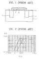
- a gate conductive layercovers the top corner portions of a trench during formation of a gate, so that an electric field is concentrated at the corners of a trench. As shown in FIG. 2, this leads to a hump phenomenon in which a transistor is turned on twice, and an inverse narrow width effect, resulting in degradation of the performance of transistors.
- FIG. 3is a graph showing an inverse narrow width effect occurring in an STI structure. As shown in this graph, an inverse narrow width effect represents a reduction in threshold voltage with a decrease in the channel width of a transistor.
- reference character Xrepresents data acquired before a hump phenomenon occurs
- reference character Yrepresents data acquired after a hump phenomenon occurs.
- the second problem occurring when the edge portions of a trench are formed with a sharp angle of almost 90°is degradation of the reliability of devices, such as, the dielectric breakdown of a gate oxide film caused by formation of a thin gate oxide film at the edge portions of a trench or by concentration of an electric field on the gate oxide film around the edges of a trench.
- U.S. Pat. No. 5,861,104discloses a method of rounding the upper corners of a trench by improving a method of etching a trench.
- U.S. Pat. No. 5,763,315discloses a method of rounding the upper edges of a trench by forming a (111) plane having a high oxidation rate on a semiconductor substrate with (100) crystal planes, using a wet etching technique or the like, and of preventing a degradation in the reliability of transistors and a gate oxide film by increasing the thickness of the gate oxide film which is formed on the upper edges of a trench.
- the present inventionintends to provide a structure for forming a (111) crystal plane on the upper edges of a trench to increase the thickness of a gate oxide film to be formed on these regions while rounding the upper edges of a trench, resulting in a significant improvement in the characteristics of transistors, and a fabrication method thereof.
- An object of the present inventionis to provide a trench isolation structure which can improve the reliability of transistors and a gate dielectric film by increasing the thickness of a gate oxide film at the upper edges of a trench while simultaneously rounding the upper edges of a trench.
- Another object of the present inventionis to provide a semiconductor device having an improved isolation structure, so that a hump phenomenon and an inverse narrow width effect are prevented.
- Still another object of the present inventionis to provide a trench isolation method by which the upper edges of a trench are rounded, and thus the thickness of a gate oxide film at the upper edges of a trench is increased.
- the first objectis achieved by a trench isolation structure including: a trench formed in non-active regions of a semiconductor substrate, the top edges of the trench being rounded; an inner wall oxide film formed on the inner wall of the trench; a liner formed on the surface of the inner wall oxide film, the top of the liner being recessed from the surface of the semiconductor substrate; and a dielectric film for filling the trench in which the inner wall oxide film and the liner have been formed.
- the inner wall oxide filmhas a thickness of 10 to 150 ⁇ , and that the top ends of the liner are recessed by 0 to 500 ⁇ from the surface of the semiconductor substrate, so that the upper edges of a trench are satisfactorily rounded.
- the second objectis achieved by a semiconductor device having a trench isolation structure, including: a trench formed in non-active regions of a semiconductor substrate, the top edges of the trench being rounded; an inner wall oxide film formed on the inner wall of the trench; a liner formed on the surface of the inner wall oxide film, the top of the liner being recessed from the surface of the semiconductor substrate; a dielectric film for filling the trench in which the inner wall oxide film and the liner have been formed; a gate dielectric film formed on active regions of the semiconductor substrate except for the trench, the edge portions of the gate dielectric film being thicker than the central portion; and a gate electrode formed on the gate dielectric film.
- the surface of the semiconductor substrate other than in the trenchhas a (100) plane
- the surface of a semiconductor substrate rounded at the top edges of the trenchhas a (111) plane.
- the third objectis achieved by a trench isolation method including: forming a trench in non-active regions of a semiconductor substrate; forming an inner wall oxide film on the inner wall of the trench; forming a silicon nitride liner on the surface of the inner wall oxide film; filling the trench with a dielectric film; and etching part of the silicon nitride liner so that the top ends of the silicon nitride liner are recessed from the surface of the semiconductor substrate.
- the step of forming the trenchincludes: forming a pad oxide film on the semiconductor substrate; forming a pad nitride film on the pad oxide film; forming an etch mask pattern for defining regions on which the trenches are to be formed, using a photolithographic process; and forming the trenches by etching parts of the semiconductor substrate using the etch mask pattern.
- the step of filling the trench with a dielectric filmincludes: depositing a dielectric film on the resultant substrate on which the inner wall oxide film and the silicon nitride liner have been formed; and planarizing the surface of the dielectric film,
- Planarization of the dielectric filmis achieved by chemical mechanical polishing (CMP) or etchback using the pad nitride film as an etch stop layer.
- CMPchemical mechanical polishing
- the step of removing a pad nitride film which remains on the active regions of the semiconductor substrateis further included after the step of planarizing the surface of the dielectric film.
- the step of removing the pad nitride filmis followed by the step of etching part of the silicon nitride liner so that the top ends of the silicon nitride liner are recessed from the surface of the semiconductor substrate.
- the step of removing the pad nitride filmis performed by wet etching.
- the step of removing the pad oxide filmis further included.
- the step of removing the pad oxide filmcan be followed by the step of oxidizing the surface of the semiconductor substrate.
- the amount of oxidation at the upper edges of a trenchcan be greatly increased in an oxidation process for forming a gate oxide film. This is accomplished by limiting the thickness of an inner wall oxide film formed on the inner wall of a trench to a certain level and forming a dent where the top portion of a liner is recessed from the surface of a semiconductor substrate. That is, the amount of oxidation at the upper edges of a trench in a semiconductor substrate is increased during subsequent oxidation for forming a gate oxide film, without rounding the upper edges of a trench on purpose, which results in rounding of the upper edges of a trench.
- the thickness of a gate oxide film at the upper edges of a trenchis greater than at the center of an active region of a semiconductor substrate outside the trench.
- FIG. 1is a cross-sectional view to explain a problem which has been encountered in a conventional shallow trench isolation (STI) method;
- STIshallow trench isolation
- FIG. 2is a graph showing a hump phenomenon occurring in a semiconductor device fabricated by a conventional STI method
- FIG. 3is a graph showing an inverse narrow width effect occurring in an STI structure
- FIG. 4is a cross-sectional view of a semiconductor device according to an embodiment of the present invention.
- FIGS. 5A through 5Fare cross-sectional views for illustrating a method of fabricating a semiconductor device having an isolation structure in which the upper edges of a trench are rounded, according to a preferred embodiment of the present invention
- FIG. 6is a partially magnified cross-sectional view showing a dent formed in a nitride liner on the top of a trench;
- FIG. 7is a partially magnified view for explaining an increase in the amount of oxidation on the top of a trench by tensile stress in a nitride liner on the inner wall of a trench;
- FIGS. 8 through 10are scan electron microscope (SEM) pictures taken to ascertain the thickness of a gate oxide film at the upper edges of a trench and the degree of edge rounding, according to the thickness of an oxide layer formed on the inner wall of a trench.
- SEMscan electron microscope
- FIG. 4shows a semiconductor device having an isolation device in which the upper edges of a trench are rounded, according to an embodiment of the present invention.
- trenchesthe upper edges of which are rounded toward an active region on which a semiconductor device is to be formed, are formed in non-active regions that are the isolation regions of a semiconductor substrate 40 .
- An inner wall oxide film 48 and a liner 50are sequentially formed along the inner wall of each of the trenches.
- the inner wall oxide film 48is formed to a thickness of about 10 to 150 ⁇ by wet or dry thermal oxidation.
- the liner 50is formed of a nitride film, particularly, a silicon nitride film, by low pressure chemical vapor deposition (LPCVD) to a thickness of about 20 to 200 ⁇ .
- LPCVDlow pressure chemical vapor deposition
- the liner 50is recessed from the surface of the semiconductor substrate 40 outside the trench, preferably recessed from the top of the trench, by a depth of about 0 to 500 ⁇ .
- the trench on which the inner wall oxide film and the liner have been formedis completely filled with a dielectric film 52 such as a CVD oxide film, and the dielectric film 52 has a planarized surface thereon.
- a dielectric film 52such as a CVD oxide film
- a gate oxide film 54which is a gate dielectric film, and a gate electrode 56 are formed on the active regions of the semiconductor substrate 40 .
- the gate oxide film 54is formed considerably thicker at the upper edges of a trench than on the surface of the semiconductor substrate 40 .
- the upper edges of a trenchare rounded, and a gate oxide film is formed thicker at the upper edges of a trench than on the active regions of a semiconductor substrate. This leads to suppression of a hump phenomenon and an inverse narrow width effect caused by concentration of an electric field at the edges of a gate oxide film, and an improvement in the reliability of a gate dielectric film.
- FIGS. 5A through 5Fare cross-sectional views for illustrating a method of fabricating a semiconductor device having an isolation structure in which the upper edges of a trench are rounded, according to a preferred embodiment of the present invention.
- a pad oxide film 42 for alleviating stress on a substrate and protecting the substrateis formed by growing a thermal oxide film of about 100 ⁇ in thickness on a semiconductor substrate 40 .
- a material having an excellent etch selectivity with respect to the semiconductor substrate 40for example, a silicon nitride film, is deposited on the pad oxide film 42 to a thickness of about 1500 ⁇ by low pressure chemical vapor deposition (LPCVD), thereby forming a pad nitride film 44 .
- the pad nitride film 44acts as an etch mask during substrate etching to form a subsequent trench or during planarization of a trench filler.
- a photoresist pattern 46which is patterned so that non-active regions where trenches are to be formed can be exposed, is formed on the pad nitride film 44 by photolithography.
- the pad nitride film 44 and the pad oxide film 42are anisotropically etched using the photoresist pattern 46 as an etch mask so that the non-active regions of the semiconductor substrate 40 are exposed.
- only the pad nitride film 44can be anisotropically etched using the photoresist pattern 46 as an etch mask to form an etch mask pattern.
- a trench 47is formed by anisotropically etching exposed portions of the semiconductor substrate 40 by about 2000 to 10000 ⁇ using the pad nitride film 44 and the pad oxide film 42 as etch mask patterns.
- the trench 47can be formed using the photoresist pattern 46 as an etch mask pattern without removing the photoresist pattern 46 .
- the trench 47can be formed substantially perpendicular to the semiconductor substrate without a special process for rounding the upper edges.
- an inner wall oxide film 48is formed along the inner wall of the trench 47 by a predetermined thermal oxidation on the semiconductor substrate 40 having the trenches 47 .
- the inner wall oxide film 48is formed to a thickness of about 10 to 150 ⁇ , preferably, to about 10 to 50 ⁇ . The reason why the inner wall oxide film is formed to be thin will be described later.
- the inner wall oxide film 48can be formed by wet oxidation or dry oxidation, preferably, by dry oxidation in which the thickness of an oxide film is easily controlled and its uniformity is high.
- a liner 50is formed by depositing a nitride film, for example, a silicon nitride film, on the entire surface of a resultant substrate on which the inner oxide film 48 is formed, by LPCVD.
- the liner 50can be formed to a thickness of about 20 to 200 ⁇ .
- a very thin lineris prone to break by a subsequent oxidation process.
- a very thick linerincreases the aspect ratio of a trench, which may lead to difficulty in achieving perfect trench filling, such as, formation of voids when the trench is filled with a dielectric film.
- a dielectric materialis deposited on the resultant structure on which the nitride film liner 50 has been formed, to a thickness that can sufficiently fill the trench, for example, equal to or less than 10000 ⁇ , by CVD or other techniques, thereby forming an oxide film 52 .
- annealingis performed at a high temperature to densify the CVD oxide film.
- the densification of the CVD oxide film 52 filling the trenchis conducted to slow down the speed of chemical mechanical polishing (CMP) which is high during subsequent planarization of the CVD oxide film 52 because of the high etch rate of the CVD oxide film 52 , and to prevent the CVD oxide film 52 from being easily consumed during wet etching of the pad oxide film 42 or during a cleaning process using an etchant.
- CMPchemical mechanical polishing
- the densification of the CVD oxide film 52is conducted at 1000° C. in a nitrogen gas (N 2 ) ambience, or achieved by wet oxidation. During this process, the semiconductor substrate 40 is not oxidized by the protection of the nitride liner 50 .
- the CVD oxide film 52is planarized, for example, by etchback, CMP or combination of etchback and CMP. If CMP is performed, it is preferable that CMP is stopped when about half the thickness of the pad nitride film 44 , which is used as an etch stop layer, is etched.
- the pad nitride film remaining on the active regionsis removed by a phophoric acid solution.
- over-etchingis performed to also etch part of the nitride film liner 50 , thereby forming a so-called “dent” where the top of the nitride liner 50 is recessed about 0 to 500 ⁇ lower than the surface of the semiconductor substrate 40 .
- a magnification of a semiconductor substrate having the dentis shown in FIG. 6 .
- oxidation of the upper edges of a trench in a semiconductor substrategreatly increases. The reason for the increase of oxidation described above will be described later.
- a dentis formed very deeply, the top of the trench becomes open, so that the top edges of the trench are sharp-pointed during oxidation.
- the top edges of a trenchremain even after a conductive material for a gate is patterned, which may cause a bridge.
- a dent recessed to 500 ⁇ or less from the surface of the semiconductor substrate 40is formed.
- the pad oxide film 42 remaining in the active regionsis removed using a diluted hydrofluoric acid (HF) solution.
- HFhydrofluoric acid
- a gate oxide film 54when a gate oxide film 54 is formed by thermal oxidation on the resultant structure of FIG. 5E, it is formed thicker at the top edges of a trench than the other portions, since oxidation at the top edges of a trench is increased as shown in this figure. Thus, the top edges of a trench become rounded. Then, a conductive material, for example, an impurity-doped polysilicon film or a stacked film of doped polysilicon and silicide, is formed on the gate oxide film 54 , and then patterned by photolithography, thereby forming a gate electrode 56 .
- a conductive materialfor example, an impurity-doped polysilicon film or a stacked film of doped polysilicon and silicide
- the thickness of the gate oxide film 54 at the top edges of a trenchbecomes greater than that of the gate oxide film 54 at the central portion of the active region of the semiconductor substrate 40 due to an increase in oxidation at the top edges of a trench. This can be considered to occur largely by the following three causes.
- the first causecan be tensile stress on the nitride liner 50 formed on the inner wall of a trench.
- FIG. 7is a partially magnified view of the sidewall of a trench.
- reference numeral 40denotes a semiconductor substrate
- reference numeral 50denotes a nitride liner.
- the inner wall oxide film formed on the inner wall of the trenchis ignored to simplify explanation.
- the silicon nitride liner 50 deposited by LPCVDcauses tensile stress on a portion B of the semiconductor substrate 40 which is near the surface of the active region. That is, since a silicon nitride film formed by LPCVD has a high thermal expansion coefficient compared to a silicon substrate, it expands more than the semiconductor substrate 40 formed of silicon single crystal during a high temperature process such as oxidation. Accordingly, the silicon nitride liner 50 is subject to tensile stress, while a portion A of the semiconductor substrate 40 on the sidewall of a trench in contact with the silicon nitride liner 50 is subject to compressive stress.
- the portion B of the semiconductor substrate 40 near the surface of the active regionis subject to tensile stress, In this state where tensile stress has been applied, the length between the crystal lattices in the semiconductor substrate is long, so that oxidation occurs fast.
- the thinner an inner wall oxide film between the silicon nitride liner 50 and the sidewall of a trenchthe better.
- the thickness of the inner wall oxide filmis kept within the range of about 10 to 150 ⁇ .
- the second causecan be formation of a dent in the silicon nitride liner 50 .
- a slanted surfaceis gradually formed while the semiconductor substrate 40 at the top edges of a trench exposed by a dent is being oxidized.
- This slanted surfacehas a (111) plane, and the surface of the active region of the semiconductor substrate 40 has a (100) plane. Since the interval between silicon crystal lattices is the greatest in the direction of the (111) plane, the bonding force between crystal lattices is weak. Accordingly, the bonding between silicon atoms located at each lattice point is easily cut during oxidation, so that oxidation occurs at the highest speed.
- the third causecan be action of the silicon nitride liner 50 as an oxidation barrier.
- oxygen atomspenetrate the CVD oxide film 48 filled in a trench and are diffused into the semiconductor substrate 40 below the sidewall of a trench, while the gate oxide film 54 of FIG. 5F is formed. Accordingly, oxidation also occurs on the sidewall of a trench. This leads to size expansion, and thus compressive stress is applied to the top edges of the semiconductor substrate 40 , so that oxidation is suppressed.
- oxidation into the side of a trench on which the liner 50 is formedis prevented by the presence of the liner 50 , while oxidation easily occurs at the top edges of a trench where the liner 50 is recessed, since the oxidation prevention factor, that is, the liner 50 , is removed.
- FIGS. 8 through 10are scan electron microscope (SEM) pictures taken to ascertain the thickness of a gate oxide film at the upper edges of a trench and the degree of edge rounding, according to the thickness of an inner wall oxide film formed on the inner wall of a trench.
- the inner wall oxide filmis formed to thicknesses of 240 ⁇ , 110 ⁇ and 20 ⁇ , respectively, a liner is formed to the same thickness, and the gate oxide film is grown to a thickness of 75 ⁇ .
- a slanted surface having a (111) planeis not formed at the top edges of a semiconductor substrate even when oxidation for forming a gate oxide film is performed. This is another reason why the corners of a trench are not rounded and the thickness of a gate oxide film is not increased.
- FIG. 9is an SEM picture of a case where an inner wall oxide film is formed to a thickness of 110 ⁇ and a dent having a desirable depth is formed after a liner is formed. It can be seen from FIG. 9 that the top corners of a trench are rounded.
- FIG. 10is an SEM picture of a case where oxidation toward the side surface of a trench is extremely limited by the formation of an inner wall oxide film to a thickness of 20 ⁇ within the trench, and the influence of tensile stress on a liner is maximized. It can be seen from FIG. 10 that the top edges of a trench are rounded and a gate oxide film at the top edges of a trench is about 170 ⁇ thick that is significantly thicker than that on the surface of active regions.
- the amount of oxidation at the top edges of a trench in a subsequent process for forming a gate oxide filmcan be greatly increased. Therefore, a hump phenomenon and an inverse narrow width effect due to concentration of an electric field at the top edges of a trench can be suppressed, and the reliability of a gate dielectric film can be improved. Furthermore, a dent recessed from the surface of a semiconductor substrate is formed in a liner formed on the inner wall oxide film, so that the crystal state of a semiconductor substrate at the top edges of a trench becomes a (111) plane during formation of a gate oxide film. Thus, the amount of oxidation can be further increased.
Landscapes
- Engineering & Computer Science (AREA)
- Physics & Mathematics (AREA)
- Condensed Matter Physics & Semiconductors (AREA)
- General Physics & Mathematics (AREA)
- Manufacturing & Machinery (AREA)
- Computer Hardware Design (AREA)
- Microelectronics & Electronic Packaging (AREA)
- Power Engineering (AREA)
- Element Separation (AREA)
- Formation Of Insulating Films (AREA)
- Insulated Gate Type Field-Effect Transistor (AREA)
Abstract
Description
Claims (10)
Priority Applications (1)
| Application Number | Priority Date | Filing Date | Title |
|---|---|---|---|
| US09/911,096US6465866B2 (en) | 1999-10-12 | 2001-07-23 | Trench isolation regions having trench liners with recessed ends |
Applications Claiming Priority (4)
| Application Number | Priority Date | Filing Date | Title |
|---|---|---|---|
| KR99-43989 | 1999-10-12 | ||
| KR1019990043989AKR100338767B1 (en) | 1999-10-12 | 1999-10-12 | Trench Isolation structure and semiconductor device having the same, trench isolation method |
| US09/684,822US6331469B1 (en) | 1999-10-12 | 2000-10-10 | Trench isolation structure, semiconductor device having the same, and trench isolation method |
| US09/911,096US6465866B2 (en) | 1999-10-12 | 2001-07-23 | Trench isolation regions having trench liners with recessed ends |
Related Parent Applications (1)
| Application Number | Title | Priority Date | Filing Date |
|---|---|---|---|
| US09/684,822DivisionUS6331469B1 (en) | 1999-10-12 | 2000-10-10 | Trench isolation structure, semiconductor device having the same, and trench isolation method |
Publications (2)
| Publication Number | Publication Date |
|---|---|
| US20010041421A1 US20010041421A1 (en) | 2001-11-15 |
| US6465866B2true US6465866B2 (en) | 2002-10-15 |
Family
ID=19614928
Family Applications (2)
| Application Number | Title | Priority Date | Filing Date |
|---|---|---|---|
| US09/684,822Expired - LifetimeUS6331469B1 (en) | 1999-10-12 | 2000-10-10 | Trench isolation structure, semiconductor device having the same, and trench isolation method |
| US09/911,096Expired - LifetimeUS6465866B2 (en) | 1999-10-12 | 2001-07-23 | Trench isolation regions having trench liners with recessed ends |
Family Applications Before (1)
| Application Number | Title | Priority Date | Filing Date |
|---|---|---|---|
| US09/684,822Expired - LifetimeUS6331469B1 (en) | 1999-10-12 | 2000-10-10 | Trench isolation structure, semiconductor device having the same, and trench isolation method |
Country Status (6)
| Country | Link |
|---|---|
| US (2) | US6331469B1 (en) |
| JP (1) | JP4072308B2 (en) |
| KR (1) | KR100338767B1 (en) |
| CN (1) | CN1194400C (en) |
| DE (1) | DE10050357B4 (en) |
| GB (1) | GB2360631B (en) |
Cited By (18)
| Publication number | Priority date | Publication date | Assignee | Title |
|---|---|---|---|---|
| US20020074614A1 (en)* | 2000-12-15 | 2002-06-20 | Mitsubishi Denki Kabushiki Kaisha | Semiconductor device and manufacturing method therefor |
| US20030020102A1 (en)* | 2001-07-24 | 2003-01-30 | Koninklijke Philips Electronics N.V. | Trench-gate semiconductor devices, and their manufacture |
| US20030173641A1 (en)* | 2002-03-18 | 2003-09-18 | Fujitsu Limited | Semiconductor device with STI and its manufacture |
| US20030181022A1 (en)* | 2002-03-21 | 2003-09-25 | Freidoon Mehrad | Method to improve STI nano gap fill and moat nitride pull back |
| US6657276B1 (en)* | 2001-12-10 | 2003-12-02 | Advanced Micro Devices, Inc. | Shallow trench isolation (STI) region with high-K liner and method of formation |
| US6833330B1 (en)* | 2001-08-13 | 2004-12-21 | Cypress Semiconductor Corporation | Method to eliminate inverse narrow width effect in small geometry MOS transistors |
| US20040266136A1 (en)* | 2003-06-30 | 2004-12-30 | Tae-Woo Jung | Method for fabricating semiconductor device having trench type device isolation layer |
| US20050070089A1 (en)* | 2003-09-29 | 2005-03-31 | Taikan Iinuma | Method for manufacturing a semiconductor device |
| US20050196913A1 (en)* | 2002-10-07 | 2005-09-08 | Promos Technologies Inc. | Floating gate memory structures and fabrication methods |
| US20060251879A1 (en)* | 2002-09-16 | 2006-11-09 | Messier Pierre J | Electrostatically charged filter media incorporating an active agent |
| US7394125B1 (en)* | 2004-03-30 | 2008-07-01 | Fasl Llc | Recessed channel with separated ONO memory device |
| US20080246111A1 (en)* | 2007-04-05 | 2008-10-09 | Taiwan Semiconductor Manufacturing Co., Ltd. | Semiconductor device and method of fabricating the same |
| US20090101943A1 (en)* | 2007-10-17 | 2009-04-23 | Toshiba America Electronic Components, Inc. | Reversely Tapered Contact Structure Compatible With Dual Stress Liner Process |
| US20110037110A1 (en)* | 2004-03-15 | 2011-02-17 | Fujitsu Semiconductor Limited | Capacitor and method for fabricationg the same, and semiconductor device and method for fabricating the same |
| US20110097889A1 (en)* | 2009-10-27 | 2011-04-28 | Taiwan Semiconductor Manufacturing Company, Ltd. | STI Shape Near Fin Bottom of Si Fin in Bulk FinFET |
| US9865495B2 (en) | 2015-11-05 | 2018-01-09 | Samsung Electronics Co., Ltd. | Semiconductor device and method for fabricating the same |
| US10181429B2 (en) | 2016-05-24 | 2019-01-15 | X-Fab Semiconductor Foundries Ag | Method for the formation of transistors PDSO1 and FDSO1 on a same substrate |
| US10888267B2 (en) | 2008-11-19 | 2021-01-12 | Inspire Medical Systems, Inc. | Method of treating sleep disordered breathing |
Families Citing this family (53)
| Publication number | Priority date | Publication date | Assignee | Title |
|---|---|---|---|---|
| JP3651344B2 (en)* | 2000-02-03 | 2005-05-25 | セイコーエプソン株式会社 | Manufacturing method of semiconductor device |
| KR100674896B1 (en)* | 2000-07-26 | 2007-01-26 | 삼성전자주식회사 | Trench element isolation method in semiconductor integrated circuit |
| JP2002043408A (en)* | 2000-07-28 | 2002-02-08 | Nec Kansai Ltd | Manufacturing method of semiconductor device |
| KR100386946B1 (en)* | 2000-08-01 | 2003-06-09 | 삼성전자주식회사 | Shallow trench isolation type semiconductor devices and method of forming it |
| US6537895B1 (en)* | 2000-11-14 | 2003-03-25 | Atmel Corporation | Method of forming shallow trench isolation in a silicon wafer |
| US6958518B2 (en)* | 2001-06-15 | 2005-10-25 | Agere Systems Inc. | Semiconductor device having at least one source/drain region formed on an isolation region and a method of manufacture therefor |
| JP5121102B2 (en) | 2001-07-11 | 2013-01-16 | ルネサスエレクトロニクス株式会社 | Manufacturing method of semiconductor device |
| KR100389929B1 (en)* | 2001-07-28 | 2003-07-04 | 삼성전자주식회사 | SOI device having trench isolation and method for manufacturing the same |
| JP3577024B2 (en)* | 2001-10-09 | 2004-10-13 | エルピーダメモリ株式会社 | Semiconductor device and manufacturing method thereof |
| US6746933B1 (en)* | 2001-10-26 | 2004-06-08 | International Business Machines Corporation | Pitcher-shaped active area for field effect transistor and method of forming same |
| US7439141B2 (en)* | 2001-12-27 | 2008-10-21 | Spansion, Llc | Shallow trench isolation approach for improved STI corner rounding |
| KR100412138B1 (en)* | 2001-12-27 | 2003-12-31 | 주식회사 하이닉스반도체 | Method for forming isolation layer of semiconductor device |
| US6838392B1 (en)* | 2002-03-15 | 2005-01-04 | Cypress Semiconductor Corporation | Methods of forming semiconductor structures, and articles and devices formed thereby |
| TWI252565B (en)* | 2002-06-24 | 2006-04-01 | Hitachi Ltd | Semiconductor device and manufacturing method thereof |
| US6734082B2 (en)* | 2002-08-06 | 2004-05-11 | Chartered Semiconductor Manufacturing Ltd. | Method of forming a shallow trench isolation structure featuring a group of insulator liner layers located on the surfaces of a shallow trench shape |
| US6809386B2 (en)* | 2002-08-29 | 2004-10-26 | Micron Technology, Inc. | Cascode I/O driver with improved ESD operation |
| JP2004152851A (en)* | 2002-10-29 | 2004-05-27 | Oki Electric Ind Co Ltd | Method of manufacturing semiconductor device |
| JP2004193585A (en)* | 2002-11-29 | 2004-07-08 | Fujitsu Ltd | Semiconductor device manufacturing method and semiconductor device |
| KR100557562B1 (en)* | 2002-12-30 | 2006-03-03 | 주식회사 하이닉스반도체 | Manufacturing method of semiconductor device |
| JP4694769B2 (en) | 2003-01-27 | 2011-06-08 | エルピーダメモリ株式会社 | Manufacturing method of semiconductor device |
| JP2004311487A (en)* | 2003-04-02 | 2004-11-04 | Hitachi Ltd | Method for manufacturing semiconductor device |
| US6853031B2 (en)* | 2003-04-17 | 2005-02-08 | United Microelectronics Corp. | Structure of a trapezoid-triple-gate FET |
| US7019380B2 (en) | 2003-06-20 | 2006-03-28 | Kabushiki Kaisha Toshiba | Semiconductor device |
| JP4825402B2 (en)* | 2004-01-14 | 2011-11-30 | ルネサスエレクトロニクス株式会社 | Manufacturing method of semiconductor device |
| JP4577680B2 (en)* | 2004-04-13 | 2010-11-10 | エルピーダメモリ株式会社 | Manufacturing method of semiconductor device |
| KR100530496B1 (en)* | 2004-04-20 | 2005-11-22 | 삼성전자주식회사 | Semiconductor device, method of forming a recess gate electrode and method of manufacturing a semiconductor device having the same |
| JP4813778B2 (en)* | 2004-06-30 | 2011-11-09 | 富士通セミコンダクター株式会社 | Semiconductor device |
| JP2006049413A (en)* | 2004-08-02 | 2006-02-16 | Fujitsu Ltd | Semiconductor device and manufacturing method thereof |
| US7339253B2 (en)* | 2004-08-16 | 2008-03-04 | Taiwan Semiconductor Manufacturing Company | Retrograde trench isolation structures |
| JP2006093216A (en)* | 2004-09-21 | 2006-04-06 | Toshiba Corp | Semiconductor device |
| KR100694976B1 (en)* | 2004-12-20 | 2007-03-14 | 주식회사 하이닉스반도체 | Device Separating Method of Semiconductor Device |
| KR100762230B1 (en)* | 2004-12-30 | 2007-10-01 | 주식회사 하이닉스반도체 | Manufacturing Method of Semiconductor Device |
| JP4515951B2 (en)* | 2005-03-31 | 2010-08-04 | 富士通セミコンダクター株式会社 | Semiconductor device and manufacturing method thereof |
| KR100699843B1 (en)* | 2005-06-09 | 2007-03-27 | 삼성전자주식회사 | Morse field effect transistor with trench isolation region and manufacturing method |
| US7265015B2 (en)* | 2005-06-30 | 2007-09-04 | Promos Technologies Inc. | Use of chlorine to fabricate trench dielectric in integrated circuits |
| US7229896B2 (en)* | 2005-08-03 | 2007-06-12 | United Microelectronics Corp. | STI process for eliminating silicon nitride liner induced defects |
| DE102005037566B4 (en)* | 2005-08-09 | 2008-04-24 | Qimonda Ag | Manufacturing method for a semiconductor structure and corresponding semiconductor structure |
| JP4951978B2 (en)* | 2006-01-13 | 2012-06-13 | ソニー株式会社 | Semiconductor device and manufacturing method thereof |
| US20070224772A1 (en)* | 2006-03-21 | 2007-09-27 | Freescale Semiconductor, Inc. | Method for forming a stressor structure |
| US8120094B2 (en)* | 2007-08-14 | 2012-02-21 | Taiwan Semiconductor Manufacturing Co., Ltd. | Shallow trench isolation with improved structure and method of forming |
| US7692483B2 (en)* | 2007-10-10 | 2010-04-06 | Atmel Corporation | Apparatus and method for preventing snap back in integrated circuits |
| CN101593717B (en)* | 2008-05-28 | 2011-06-01 | 上海华虹Nec电子有限公司 | Preparation method of shallow trench isolation structure |
| JP2010034468A (en)* | 2008-07-31 | 2010-02-12 | Renesas Technology Corp | Semiconductor device and method of manufacturing the same |
| US8125037B2 (en) | 2008-08-12 | 2012-02-28 | International Business Machines Corporation | Field effect transistor with channel region edge and center portions having different band structures for suppressed corner leakage |
| US7838353B2 (en)* | 2008-08-12 | 2010-11-23 | International Business Machines Corporation | Field effect transistor with suppressed corner leakage through channel material band-edge modulation, design structure and method |
| US8085604B2 (en)* | 2008-12-12 | 2011-12-27 | Atmel Corporation | Snap-back tolerant integrated circuits |
| JP5357121B2 (en) | 2010-09-16 | 2013-12-04 | シャープ株式会社 | Semiconductor device manufacturing method and electrical apparatus |
| CN102543760B (en)* | 2012-02-28 | 2014-06-04 | 上海华力微电子有限公司 | Method for increasing shallow trench isolating compressive stress and improving NMOS electron mobility |
| CN105097639A (en)* | 2014-04-21 | 2015-11-25 | 中芯国际集成电路制造(上海)有限公司 | Semiconductor device and manufacture method thereof |
| CN111341724B (en)* | 2018-12-19 | 2022-11-04 | 上海新微技术研发中心有限公司 | Shallow trench isolation process and shallow trench isolation structure |
| US12438035B2 (en) | 2020-03-18 | 2025-10-07 | Rohm Co., Ltd. | Semiconductor device and method for manufacturing the same |
| TWI766294B (en)* | 2020-06-10 | 2022-06-01 | 聯華電子股份有限公司 | Method of forming isolation structure |
| CN112234024A (en)* | 2020-11-18 | 2021-01-15 | 华虹半导体(无锡)有限公司 | Corner Rounding Method for Shallow Trench Isolation Structure |
Citations (74)
| Publication number | Priority date | Publication date | Assignee | Title |
|---|---|---|---|---|
| US4352724A (en) | 1979-11-28 | 1982-10-05 | Fujitsu Limited | Method of manufacturing a semiconductor device |
| EP0071204A2 (en) | 1981-07-27 | 1983-02-09 | International Business Machines Corporation | Method for forming recessed dielectric isolation |
| US4390393A (en) | 1981-11-12 | 1983-06-28 | General Electric Company | Method of forming an isolation trench in a semiconductor substrate |
| US4571819A (en) | 1984-11-01 | 1986-02-25 | Ncr Corporation | Method for forming trench isolation structures |
| JPS61137338A (en) | 1984-12-10 | 1986-06-25 | Hitachi Ltd | Method for manufacturing semiconductor integrated circuit device |
| US4631803A (en) | 1985-02-14 | 1986-12-30 | Texas Instruments Incorporated | Method of fabricating defect free trench isolation devices |
| US4636281A (en) | 1984-06-14 | 1987-01-13 | Commissariat A L'energie Atomique | Process for the autopositioning of a local field oxide with respect to an insulating trench |
| US4656497A (en) | 1984-11-01 | 1987-04-07 | Ncr Corporation | Trench isolation structures |
| US4825277A (en) | 1987-11-17 | 1989-04-25 | Motorola Inc. | Trench isolation process and structure |
| US4826887A (en) | 1985-11-14 | 1989-05-02 | Shell Oil Company | Process for the preparation of polycarbonates |
| US4960727A (en) | 1987-11-17 | 1990-10-02 | Motorola, Inc. | Method for forming a dielectric filled trench |
| US5189501A (en) | 1988-10-05 | 1993-02-23 | Sharp Kabushiki Kaisha | Isolator for electrically isolating semiconductor devices in an integrated circuit |
| US5190889A (en) | 1991-12-09 | 1993-03-02 | Motorola, Inc. | Method of forming trench isolation structure with germanium silicate filling |
| EP0532361A2 (en) | 1991-09-13 | 1993-03-17 | Nec Corporation | Method of manufacturing semiconductor device |
| US5206182A (en) | 1989-06-08 | 1993-04-27 | United Technologies Corporation | Trench isolation process |
| US5223736A (en) | 1989-09-27 | 1993-06-29 | Texas Instruments Incorporated | Trench isolation process with reduced topography |
| US5316965A (en) | 1993-07-29 | 1994-05-31 | Digital Equipment Corporation | Method of decreasing the field oxide etch rate in isolation technology |
| US5387539A (en) | 1992-06-18 | 1995-02-07 | Hyundai Electronics Industries Co., Ltd. | Method of manufacturing trench isolation |
| US5447884A (en) | 1994-06-29 | 1995-09-05 | International Business Machines Corporation | Shallow trench isolation with thin nitride liner |
| US5472904A (en) | 1994-03-02 | 1995-12-05 | Micron Technology, Inc. | Thermal trench isolation |
| US5474953A (en) | 1991-11-28 | 1995-12-12 | Nec Corporation | Method of forming an isolation region comprising a trench isolation region and a selective oxidation film involved in a semiconductor device |
| US5492858A (en) | 1994-04-20 | 1996-02-20 | Digital Equipment Corporation | Shallow trench isolation process for high aspect ratio trenches |
| US5521422A (en) | 1994-12-02 | 1996-05-28 | International Business Machines Corporation | Corner protected shallow trench isolation device |
| US5554256A (en) | 1993-09-23 | 1996-09-10 | U.S. Philips Corporation | Method of manufacturing a semiconductor device having a semiconductor body with field insulation regions formed by grooves filled with insulating material |
| US5561073A (en) | 1992-03-13 | 1996-10-01 | Jerome; Rick C. | Method of fabricating an isolation trench for analog bipolar devices in harsh environments |
| US5578518A (en) | 1993-12-20 | 1996-11-26 | Kabushiki Kaisha Toshiba | Method of manufacturing a trench isolation having round corners |
| US5612242A (en) | 1996-03-11 | 1997-03-18 | United Microelectronics Corp. | Trench isolation method for CMOS transistor |
| US5643823A (en) | 1995-09-21 | 1997-07-01 | Siemens Aktiengesellschaft | Application of thin crystalline Si3 N4 liners in shallow trench isolation (STI) structures |
| US5674775A (en) | 1997-02-20 | 1997-10-07 | Taiwan Semiconductor Manufacturing Company, Ltd. | Isolation trench with a rounded top edge using an etch buffer layer |
| US5677234A (en) | 1995-06-22 | 1997-10-14 | Samsung Electronics Co., Ltd. | Methods of forming isolated semiconductor device active regions |
| US5677233A (en) | 1995-12-25 | 1997-10-14 | Nec Corporation | Process of fabricating semiconductor device having isolating oxide rising out of groove |
| US5679599A (en) | 1995-06-22 | 1997-10-21 | Advanced Micro Devices, Inc. | Isolation using self-aligned trench formation and conventional LOCOS |
| US5696020A (en) | 1994-11-23 | 1997-12-09 | Electronics And Telecommunications Research Institute | Method for fabricating semiconductor device isolation region using a trench mask |
| US5712205A (en) | 1995-11-21 | 1998-01-27 | Hyundai Electronics Industries Co., Ltd. | Semiconductor isolation method |
| US5712185A (en) | 1996-04-23 | 1998-01-27 | United Microelectronics | Method for forming shallow trench isolation |
| US5719085A (en) | 1995-09-29 | 1998-02-17 | Intel Corporation | Shallow trench isolation technique |
| US5728621A (en) | 1997-04-28 | 1998-03-17 | Chartered Semiconductor Manufacturing Pte Ltd | Method for shallow trench isolation |
| US5750433A (en) | 1996-06-25 | 1998-05-12 | Samsung Electronics Co., Ltd. | Methods of forming electrically isolated active region pedestals using trench-based isolation techniques |
| US5753562A (en) | 1996-09-05 | 1998-05-19 | Samsung Electronics Co., Ltd. | Methods of forming semiconductor devices in substrates having inverted-trench isolation regions therein |
| US5763315A (en) | 1997-01-28 | 1998-06-09 | International Business Machines Corporation | Shallow trench isolation with oxide-nitride/oxynitride liner |
| US5780346A (en) | 1996-12-31 | 1998-07-14 | Intel Corporation | N2 O nitrided-oxide trench sidewalls and method of making isolation structure |
| US5786262A (en) | 1997-04-09 | 1998-07-28 | Taiwan Semiconductor Manufacturing Co., Ltd. | Self-planarized gapfilling for shallow trench isolation |
| US5834358A (en) | 1996-11-12 | 1998-11-10 | Micron Technology, Inc. | Isolation regions and methods of forming isolation regions |
| US5837612A (en) | 1997-08-01 | 1998-11-17 | Motorola, Inc. | Silicon chemical mechanical polish etch (CMP) stop for reduced trench fill erosion and method for formation |
| US5837595A (en) | 1996-06-07 | 1998-11-17 | Samsung Electronics Co., Ltd. | Methods of forming field oxide isolation regions with reduced susceptibility to polysilicon residue defects |
| US5858842A (en) | 1996-07-03 | 1999-01-12 | Samsung Electronics Co., Ltd. | Methods of forming combined trench and locos-based electrical isolation regions in semiconductor substrates |
| US5861104A (en) | 1996-03-28 | 1999-01-19 | Advanced Micro Devices | Trench isolation with rounded top and bottom corners and edges |
| US5863827A (en) | 1997-06-03 | 1999-01-26 | Texas Instruments Incorporated | Oxide deglaze before sidewall oxidation of mesa or trench |
| US5866465A (en) | 1997-04-03 | 1999-02-02 | Micron Technology, Inc. | Semiconductor processing method of forming a contact opening to a region adjacent a field isolation mass |
| US5872045A (en) | 1997-07-14 | 1999-02-16 | Industrial Technology Research Institute | Method for making an improved global planarization surface by using a gradient-doped polysilicon trench--fill in shallow trench isolation |
| US5885883A (en) | 1996-04-15 | 1999-03-23 | Samsung Electronics Co., Ltd. | Methods of forming trench-based isolation regions with reduced susceptibility to edge defects |
| KR19990057708A (en) | 1997-12-30 | 1999-07-15 | 윤종용 | Trench element isolation |
| US5940716A (en) | 1996-03-15 | 1999-08-17 | Samsung Electronics Co., Ltd. | Methods of forming trench isolation regions using repatterned trench masks |
| US5977585A (en) | 1988-05-17 | 1999-11-02 | Xicor, Inc. | Deposited tunneling oxide |
| US5976951A (en) | 1998-06-30 | 1999-11-02 | United Microelectronics Corp. | Method for preventing oxide recess formation in a shallow trench isolation |
| US5989978A (en) | 1998-07-16 | 1999-11-23 | Chartered Semiconductor Manufacturing, Ltd. | Shallow trench isolation of MOSFETS with reduced corner parasitic currents |
| US5994200A (en) | 1996-12-26 | 1999-11-30 | Lg Semicon Co., Ltd. | Trench isolation structure of a semiconductor device and a method for thereof |
| US6001707A (en) | 1998-12-07 | 1999-12-14 | United Semiconductor Corp. | Method for forming shallow trench isolation structure |
| US6004862A (en) | 1998-01-20 | 1999-12-21 | Advanced Micro Devices, Inc. | Core array and periphery isolation technique |
| US6008108A (en) | 1998-12-07 | 1999-12-28 | United Microelectronics Corp. | Method of fabricating a shallow-trench isolation structure in an integrated circuit |
| US6030882A (en) | 1998-11-06 | 2000-02-29 | United Semiconductor Corp. | Method for manufacturing shallow trench isolation structure |
| US6037237A (en) | 1997-07-25 | 2000-03-14 | Samsung Electronics Co., Ltd. | Trench isolation methods utilizing composite oxide films |
| US6054343A (en) | 1998-01-26 | 2000-04-25 | Texas Instruments Incorporated | Nitride trench fill process for increasing shallow trench isolation (STI) robustness |
| US6057208A (en) | 1997-12-27 | 2000-05-02 | United Microelectronics Corp. | Method of forming shallow trench isolation |
| US6074932A (en) | 1998-01-28 | 2000-06-13 | Texas Instruments - Acer Incorporated | Method for forming a stress-free shallow trench isolation |
| US6090684A (en) | 1998-07-31 | 2000-07-18 | Hitachi, Ltd. | Method for manufacturing semiconductor device |
| US6093611A (en) | 1997-12-19 | 2000-07-25 | Advanced Micro Devices, Inc. | Oxide liner for high reliability with reduced encroachment of the source/drain region |
| US6103635A (en) | 1997-10-28 | 2000-08-15 | Fairchild Semiconductor Corp. | Trench forming process and integrated circuit device including a trench |
| US6107159A (en) | 1999-01-16 | 2000-08-22 | United Semiconductor Corp. | Method for fabricating a shallow trench isolation structure |
| EP1052690A2 (en) | 1999-05-10 | 2000-11-15 | Intersil Corporation | Process or forming MOS-gated devices having self-aligned trenches |
| US6159823A (en) | 1998-09-24 | 2000-12-12 | Samsung Electronics Co., Ltd. | Trench isolation method of semiconductor device |
| US6171928B1 (en) | 1999-08-13 | 2001-01-09 | Worldwide Semiconductor Manufacturing Corp. | Method of fabricating shallow trench insolation |
| US6187651B1 (en) | 1998-05-07 | 2001-02-13 | Samsung Electronics Co., Ltd. | Methods of forming trench isolation regions using preferred stress relieving layers and techniques to inhibit the occurrence of voids |
| US6255194B1 (en)* | 1999-06-03 | 2001-07-03 | Samsung Electronics Co., Ltd. | Trench isolation method |
Family Cites Families (5)
| Publication number | Priority date | Publication date | Assignee | Title |
|---|---|---|---|---|
| JP2663739B2 (en)* | 1991-04-08 | 1997-10-15 | 日本電気株式会社 | Method for manufacturing semiconductor device |
| JPH05304205A (en)* | 1992-04-27 | 1993-11-16 | Toshiba Corp | Semiconductor device and manufacturing method thereof |
| KR19990010757A (en)* | 1997-07-18 | 1999-02-18 | 윤종용 | Device Separation Method of Semiconductor Device |
| KR19990025197A (en)* | 1997-09-11 | 1999-04-06 | 윤종용 | Trench element isolation |
| KR100459691B1 (en)* | 1998-01-05 | 2005-01-17 | 삼성전자주식회사 | Trench isolation method of semiconductor device to improve electrical characteristic |
- 1999
- 1999-10-12KRKR1019990043989Apatent/KR100338767B1/ennot_activeExpired - Lifetime
- 2000
- 2000-10-10USUS09/684,822patent/US6331469B1/ennot_activeExpired - Lifetime
- 2000-10-11GBGB0024940Apatent/GB2360631B/ennot_activeExpired - Fee Related
- 2000-10-11DEDE10050357.8Apatent/DE10050357B4/ennot_activeExpired - Lifetime
- 2000-10-12CNCNB001347179Apatent/CN1194400C/ennot_activeExpired - Lifetime
- 2000-10-12JPJP2000312495Apatent/JP4072308B2/ennot_activeExpired - Fee Related
- 2001
- 2001-07-23USUS09/911,096patent/US6465866B2/ennot_activeExpired - Lifetime
Patent Citations (76)
| Publication number | Priority date | Publication date | Assignee | Title |
|---|---|---|---|---|
| US4352724A (en) | 1979-11-28 | 1982-10-05 | Fujitsu Limited | Method of manufacturing a semiconductor device |
| US4352724B1 (en) | 1979-11-28 | 1997-06-10 | Fujitsu Ltd | Method of manufacturing a semiconductor device |
| EP0071204A2 (en) | 1981-07-27 | 1983-02-09 | International Business Machines Corporation | Method for forming recessed dielectric isolation |
| US4390393A (en) | 1981-11-12 | 1983-06-28 | General Electric Company | Method of forming an isolation trench in a semiconductor substrate |
| US4636281A (en) | 1984-06-14 | 1987-01-13 | Commissariat A L'energie Atomique | Process for the autopositioning of a local field oxide with respect to an insulating trench |
| US4571819A (en) | 1984-11-01 | 1986-02-25 | Ncr Corporation | Method for forming trench isolation structures |
| WO1986002777A1 (en) | 1984-11-01 | 1986-05-09 | Ncr Corporation | Process for forming isolation regions in a semiconductor substrate |
| US4656497A (en) | 1984-11-01 | 1987-04-07 | Ncr Corporation | Trench isolation structures |
| JPS61137338A (en) | 1984-12-10 | 1986-06-25 | Hitachi Ltd | Method for manufacturing semiconductor integrated circuit device |
| US4631803A (en) | 1985-02-14 | 1986-12-30 | Texas Instruments Incorporated | Method of fabricating defect free trench isolation devices |
| US4826887A (en) | 1985-11-14 | 1989-05-02 | Shell Oil Company | Process for the preparation of polycarbonates |
| US4960727A (en) | 1987-11-17 | 1990-10-02 | Motorola, Inc. | Method for forming a dielectric filled trench |
| US4825277A (en) | 1987-11-17 | 1989-04-25 | Motorola Inc. | Trench isolation process and structure |
| US5977585A (en) | 1988-05-17 | 1999-11-02 | Xicor, Inc. | Deposited tunneling oxide |
| US5189501A (en) | 1988-10-05 | 1993-02-23 | Sharp Kabushiki Kaisha | Isolator for electrically isolating semiconductor devices in an integrated circuit |
| US5206182A (en) | 1989-06-08 | 1993-04-27 | United Technologies Corporation | Trench isolation process |
| US5223736A (en) | 1989-09-27 | 1993-06-29 | Texas Instruments Incorporated | Trench isolation process with reduced topography |
| EP0532361A2 (en) | 1991-09-13 | 1993-03-17 | Nec Corporation | Method of manufacturing semiconductor device |
| US5474953A (en) | 1991-11-28 | 1995-12-12 | Nec Corporation | Method of forming an isolation region comprising a trench isolation region and a selective oxidation film involved in a semiconductor device |
| US5190889A (en) | 1991-12-09 | 1993-03-02 | Motorola, Inc. | Method of forming trench isolation structure with germanium silicate filling |
| US5561073A (en) | 1992-03-13 | 1996-10-01 | Jerome; Rick C. | Method of fabricating an isolation trench for analog bipolar devices in harsh environments |
| US5387539A (en) | 1992-06-18 | 1995-02-07 | Hyundai Electronics Industries Co., Ltd. | Method of manufacturing trench isolation |
| US5316965A (en) | 1993-07-29 | 1994-05-31 | Digital Equipment Corporation | Method of decreasing the field oxide etch rate in isolation technology |
| US5554256A (en) | 1993-09-23 | 1996-09-10 | U.S. Philips Corporation | Method of manufacturing a semiconductor device having a semiconductor body with field insulation regions formed by grooves filled with insulating material |
| US5578518A (en) | 1993-12-20 | 1996-11-26 | Kabushiki Kaisha Toshiba | Method of manufacturing a trench isolation having round corners |
| US5472904A (en) | 1994-03-02 | 1995-12-05 | Micron Technology, Inc. | Thermal trench isolation |
| US5492858A (en) | 1994-04-20 | 1996-02-20 | Digital Equipment Corporation | Shallow trench isolation process for high aspect ratio trenches |
| US5447884A (en) | 1994-06-29 | 1995-09-05 | International Business Machines Corporation | Shallow trench isolation with thin nitride liner |
| US5696020A (en) | 1994-11-23 | 1997-12-09 | Electronics And Telecommunications Research Institute | Method for fabricating semiconductor device isolation region using a trench mask |
| US5521422A (en) | 1994-12-02 | 1996-05-28 | International Business Machines Corporation | Corner protected shallow trench isolation device |
| US5677234A (en) | 1995-06-22 | 1997-10-14 | Samsung Electronics Co., Ltd. | Methods of forming isolated semiconductor device active regions |
| US5679599A (en) | 1995-06-22 | 1997-10-21 | Advanced Micro Devices, Inc. | Isolation using self-aligned trench formation and conventional LOCOS |
| US5643823A (en) | 1995-09-21 | 1997-07-01 | Siemens Aktiengesellschaft | Application of thin crystalline Si3 N4 liners in shallow trench isolation (STI) structures |
| US5719085A (en) | 1995-09-29 | 1998-02-17 | Intel Corporation | Shallow trench isolation technique |
| US5712205A (en) | 1995-11-21 | 1998-01-27 | Hyundai Electronics Industries Co., Ltd. | Semiconductor isolation method |
| US5677233A (en) | 1995-12-25 | 1997-10-14 | Nec Corporation | Process of fabricating semiconductor device having isolating oxide rising out of groove |
| US5612242A (en) | 1996-03-11 | 1997-03-18 | United Microelectronics Corp. | Trench isolation method for CMOS transistor |
| US5940716A (en) | 1996-03-15 | 1999-08-17 | Samsung Electronics Co., Ltd. | Methods of forming trench isolation regions using repatterned trench masks |
| US5861104A (en) | 1996-03-28 | 1999-01-19 | Advanced Micro Devices | Trench isolation with rounded top and bottom corners and edges |
| US5885883A (en) | 1996-04-15 | 1999-03-23 | Samsung Electronics Co., Ltd. | Methods of forming trench-based isolation regions with reduced susceptibility to edge defects |
| US5712185A (en) | 1996-04-23 | 1998-01-27 | United Microelectronics | Method for forming shallow trench isolation |
| US5837595A (en) | 1996-06-07 | 1998-11-17 | Samsung Electronics Co., Ltd. | Methods of forming field oxide isolation regions with reduced susceptibility to polysilicon residue defects |
| US5750433A (en) | 1996-06-25 | 1998-05-12 | Samsung Electronics Co., Ltd. | Methods of forming electrically isolated active region pedestals using trench-based isolation techniques |
| US5858842A (en) | 1996-07-03 | 1999-01-12 | Samsung Electronics Co., Ltd. | Methods of forming combined trench and locos-based electrical isolation regions in semiconductor substrates |
| US5753562A (en) | 1996-09-05 | 1998-05-19 | Samsung Electronics Co., Ltd. | Methods of forming semiconductor devices in substrates having inverted-trench isolation regions therein |
| US5834358A (en) | 1996-11-12 | 1998-11-10 | Micron Technology, Inc. | Isolation regions and methods of forming isolation regions |
| US5994200A (en) | 1996-12-26 | 1999-11-30 | Lg Semicon Co., Ltd. | Trench isolation structure of a semiconductor device and a method for thereof |
| US5780346A (en) | 1996-12-31 | 1998-07-14 | Intel Corporation | N2 O nitrided-oxide trench sidewalls and method of making isolation structure |
| US5763315A (en) | 1997-01-28 | 1998-06-09 | International Business Machines Corporation | Shallow trench isolation with oxide-nitride/oxynitride liner |
| US5674775A (en) | 1997-02-20 | 1997-10-07 | Taiwan Semiconductor Manufacturing Company, Ltd. | Isolation trench with a rounded top edge using an etch buffer layer |
| US5866465A (en) | 1997-04-03 | 1999-02-02 | Micron Technology, Inc. | Semiconductor processing method of forming a contact opening to a region adjacent a field isolation mass |
| US5786262A (en) | 1997-04-09 | 1998-07-28 | Taiwan Semiconductor Manufacturing Co., Ltd. | Self-planarized gapfilling for shallow trench isolation |
| US5728621A (en) | 1997-04-28 | 1998-03-17 | Chartered Semiconductor Manufacturing Pte Ltd | Method for shallow trench isolation |
| US5863827A (en) | 1997-06-03 | 1999-01-26 | Texas Instruments Incorporated | Oxide deglaze before sidewall oxidation of mesa or trench |
| US5872045A (en) | 1997-07-14 | 1999-02-16 | Industrial Technology Research Institute | Method for making an improved global planarization surface by using a gradient-doped polysilicon trench--fill in shallow trench isolation |
| US6037237A (en) | 1997-07-25 | 2000-03-14 | Samsung Electronics Co., Ltd. | Trench isolation methods utilizing composite oxide films |
| US5837612A (en) | 1997-08-01 | 1998-11-17 | Motorola, Inc. | Silicon chemical mechanical polish etch (CMP) stop for reduced trench fill erosion and method for formation |
| US6103635A (en) | 1997-10-28 | 2000-08-15 | Fairchild Semiconductor Corp. | Trench forming process and integrated circuit device including a trench |
| US6093611A (en) | 1997-12-19 | 2000-07-25 | Advanced Micro Devices, Inc. | Oxide liner for high reliability with reduced encroachment of the source/drain region |
| US6057208A (en) | 1997-12-27 | 2000-05-02 | United Microelectronics Corp. | Method of forming shallow trench isolation |
| KR19990057708A (en) | 1997-12-30 | 1999-07-15 | 윤종용 | Trench element isolation |
| US6004862A (en) | 1998-01-20 | 1999-12-21 | Advanced Micro Devices, Inc. | Core array and periphery isolation technique |
| US6054343A (en) | 1998-01-26 | 2000-04-25 | Texas Instruments Incorporated | Nitride trench fill process for increasing shallow trench isolation (STI) robustness |
| US6074932A (en) | 1998-01-28 | 2000-06-13 | Texas Instruments - Acer Incorporated | Method for forming a stress-free shallow trench isolation |
| US6187651B1 (en) | 1998-05-07 | 2001-02-13 | Samsung Electronics Co., Ltd. | Methods of forming trench isolation regions using preferred stress relieving layers and techniques to inhibit the occurrence of voids |
| US5976951A (en) | 1998-06-30 | 1999-11-02 | United Microelectronics Corp. | Method for preventing oxide recess formation in a shallow trench isolation |
| US5989978A (en) | 1998-07-16 | 1999-11-23 | Chartered Semiconductor Manufacturing, Ltd. | Shallow trench isolation of MOSFETS with reduced corner parasitic currents |
| US6090684A (en) | 1998-07-31 | 2000-07-18 | Hitachi, Ltd. | Method for manufacturing semiconductor device |
| US6159823A (en) | 1998-09-24 | 2000-12-12 | Samsung Electronics Co., Ltd. | Trench isolation method of semiconductor device |
| US6030882A (en) | 1998-11-06 | 2000-02-29 | United Semiconductor Corp. | Method for manufacturing shallow trench isolation structure |
| US6008108A (en) | 1998-12-07 | 1999-12-28 | United Microelectronics Corp. | Method of fabricating a shallow-trench isolation structure in an integrated circuit |
| US6001707A (en) | 1998-12-07 | 1999-12-14 | United Semiconductor Corp. | Method for forming shallow trench isolation structure |
| US6107159A (en) | 1999-01-16 | 2000-08-22 | United Semiconductor Corp. | Method for fabricating a shallow trench isolation structure |
| EP1052690A2 (en) | 1999-05-10 | 2000-11-15 | Intersil Corporation | Process or forming MOS-gated devices having self-aligned trenches |
| US6255194B1 (en)* | 1999-06-03 | 2001-07-03 | Samsung Electronics Co., Ltd. | Trench isolation method |
| US6171928B1 (en) | 1999-08-13 | 2001-01-09 | Worldwide Semiconductor Manufacturing Corp. | Method of fabricating shallow trench insolation |
Non-Patent Citations (4)
| Title |
|---|
| Notice to Submit Response (Translation Included), Korean Application No. 10-1999-0043989, Aug. 30, 2001. |
| Park, et al., "Correlation between Gate Oxide Reliability and the Profile of the Trench Top Corner in Shallow Trench Isolation (STI)," International Electron Devices Meeting, 1996, pp. 747-750. |
| Search Report, Application No. GB 0024940.9; Jul. 19, 2001. |
| Stanley Wolf, Silicon Processing for the VSLI ERA, vol. 1, Lattice Press, 1986, pp. 546 and 581. |
Cited By (34)
| Publication number | Priority date | Publication date | Assignee | Title |
|---|---|---|---|---|
| US6921947B2 (en)* | 2000-12-15 | 2005-07-26 | Renesas Technology Corp. | Semiconductor device having recessed isolation insulation film |
| US20020074614A1 (en)* | 2000-12-15 | 2002-06-20 | Mitsubishi Denki Kabushiki Kaisha | Semiconductor device and manufacturing method therefor |
| US6707100B2 (en)* | 2001-07-24 | 2004-03-16 | Koninklijke Philips Electronics N.V. | Trench-gate semiconductor devices, and their manufacture |
| US6855601B2 (en)* | 2001-07-24 | 2005-02-15 | Koninklijke Philips Electronics N.V. | Trench-gate semiconductor devices, and their manufacture |
| US20030020102A1 (en)* | 2001-07-24 | 2003-01-30 | Koninklijke Philips Electronics N.V. | Trench-gate semiconductor devices, and their manufacture |
| US6833330B1 (en)* | 2001-08-13 | 2004-12-21 | Cypress Semiconductor Corporation | Method to eliminate inverse narrow width effect in small geometry MOS transistors |
| US6984569B2 (en)* | 2001-12-10 | 2006-01-10 | Advanced Micro Devices, Inc. | Shallow trench isolation (STI) region with high-K liner and method of formation |
| US20050073022A1 (en)* | 2001-12-10 | 2005-04-07 | Karlsson Olov B. | Shallow trench isolation (STI) region with high-K liner and method of formation |
| US6657276B1 (en)* | 2001-12-10 | 2003-12-02 | Advanced Micro Devices, Inc. | Shallow trench isolation (STI) region with high-K liner and method of formation |
| US7589391B2 (en) | 2002-03-18 | 2009-09-15 | Fujitsu Microelectronics Limited | Semiconductor device with STI and its manufacture |
| US20030173641A1 (en)* | 2002-03-18 | 2003-09-18 | Fujitsu Limited | Semiconductor device with STI and its manufacture |
| US20060202301A1 (en)* | 2002-03-18 | 2006-09-14 | Fujitsu Limited | Semiconductor device with STI and its manufacture |
| US6828213B2 (en)* | 2002-03-21 | 2004-12-07 | Texas Instruments Incorporated | Method to improve STI nano gap fill and moat nitride pull back |
| US20030181022A1 (en)* | 2002-03-21 | 2003-09-25 | Freidoon Mehrad | Method to improve STI nano gap fill and moat nitride pull back |
| US20060251879A1 (en)* | 2002-09-16 | 2006-11-09 | Messier Pierre J | Electrostatically charged filter media incorporating an active agent |
| US20070187748A1 (en)* | 2002-10-07 | 2007-08-16 | Chia-Shun Hsiao | Floating gate memory structures |
| US20050196913A1 (en)* | 2002-10-07 | 2005-09-08 | Promos Technologies Inc. | Floating gate memory structures and fabrication methods |
| US20070264779A1 (en)* | 2002-10-07 | 2007-11-15 | Promos Technologies Inc. | Methods for forming floating gate memory structures |
| US20040266136A1 (en)* | 2003-06-30 | 2004-12-30 | Tae-Woo Jung | Method for fabricating semiconductor device having trench type device isolation layer |
| US20050070089A1 (en)* | 2003-09-29 | 2005-03-31 | Taikan Iinuma | Method for manufacturing a semiconductor device |
| US7022584B2 (en)* | 2003-09-29 | 2006-04-04 | Oki Electric Industry Co., Ltd. | Method of manufacturing a shallow trench isolation structure |
| US8772104B2 (en) | 2004-03-15 | 2014-07-08 | Fujitsu Semiconductor Limited | Capacitor and method for fabricating the same, and semiconductor device and method for fabricating the same |
| US20110037110A1 (en)* | 2004-03-15 | 2011-02-17 | Fujitsu Semiconductor Limited | Capacitor and method for fabricationg the same, and semiconductor device and method for fabricating the same |
| US7394125B1 (en)* | 2004-03-30 | 2008-07-01 | Fasl Llc | Recessed channel with separated ONO memory device |
| US20080246111A1 (en)* | 2007-04-05 | 2008-10-09 | Taiwan Semiconductor Manufacturing Co., Ltd. | Semiconductor device and method of fabricating the same |
| US8093678B2 (en)* | 2007-04-05 | 2012-01-10 | Taiwan Semiconductor Manufacturing Co., Ltd. | Semiconductor device and method of fabricating the same |
| US20090101943A1 (en)* | 2007-10-17 | 2009-04-23 | Toshiba America Electronic Components, Inc. | Reversely Tapered Contact Structure Compatible With Dual Stress Liner Process |
| US7652335B2 (en) | 2007-10-17 | 2010-01-26 | Toshiba America Electronics Components, Inc. | Reversely tapered contact structure compatible with dual stress liner process |
| US10888267B2 (en) | 2008-11-19 | 2021-01-12 | Inspire Medical Systems, Inc. | Method of treating sleep disordered breathing |
| US12138071B2 (en) | 2008-11-19 | 2024-11-12 | Inspire Medical Systems, Inc. | Method of treating sleep disordered breathing |
| US20110097889A1 (en)* | 2009-10-27 | 2011-04-28 | Taiwan Semiconductor Manufacturing Company, Ltd. | STI Shape Near Fin Bottom of Si Fin in Bulk FinFET |
| US9953885B2 (en)* | 2009-10-27 | 2018-04-24 | Taiwan Semiconductor Manufacturing Company, Ltd. | STI shape near fin bottom of Si fin in bulk FinFET |
| US9865495B2 (en) | 2015-11-05 | 2018-01-09 | Samsung Electronics Co., Ltd. | Semiconductor device and method for fabricating the same |
| US10181429B2 (en) | 2016-05-24 | 2019-01-15 | X-Fab Semiconductor Foundries Ag | Method for the formation of transistors PDSO1 and FDSO1 on a same substrate |
Also Published As
| Publication number | Publication date |
|---|---|
| GB2360631A (en) | 2001-09-26 |
| DE10050357A1 (en) | 2001-06-28 |
| US20010041421A1 (en) | 2001-11-15 |
| GB2360631B (en) | 2003-09-03 |
| CN1293452A (en) | 2001-05-02 |
| CN1194400C (en) | 2005-03-23 |
| GB0024940D0 (en) | 2000-11-29 |
| KR20010036816A (en) | 2001-05-07 |
| KR100338767B1 (en) | 2002-05-30 |
| JP4072308B2 (en) | 2008-04-09 |
| JP2001160589A (en) | 2001-06-12 |
| DE10050357B4 (en) | 2015-07-02 |
| US6331469B1 (en) | 2001-12-18 |
Similar Documents
| Publication | Publication Date | Title |
|---|---|---|
| US6465866B2 (en) | Trench isolation regions having trench liners with recessed ends | |
| US5945724A (en) | Trench isolation region for semiconductor device | |
| US5885883A (en) | Methods of forming trench-based isolation regions with reduced susceptibility to edge defects | |
| US6699773B2 (en) | Shallow trench isolation type semiconductor device and method of forming the same | |
| KR100213196B1 (en) | Trench device separation | |
| US6121110A (en) | Trench isolation method for semiconductor device | |
| US6074927A (en) | Shallow trench isolation formation with trench wall spacer | |
| KR100363558B1 (en) | Method of forming a trench isolation in an integrated circuit device | |
| KR100341480B1 (en) | Method for self-aligned shallow trench isolation | |
| US6501148B2 (en) | Trench isolation for semiconductor device with lateral projections above substrate | |
| KR100407567B1 (en) | Trench Isolation Process Without Dent | |
| KR20000013397A (en) | Manufacturing method of trench isolation | |
| KR20060042460A (en) | Transistor manufacturing method having recess channel of semiconductor device | |
| CN1233851A (en) | Formation method of trench isolation | |
| KR100419754B1 (en) | A method for forming a field oxide of a semiconductor device | |
| KR100446285B1 (en) | Method for forming trench isolation region having round-shaped profile formed at upper corner of trench | |
| KR100223751B1 (en) | Device Separation Method of Semiconductor Device | |
| KR100195206B1 (en) | Semiconductor Device Separation Method Using Trench | |
| KR100459693B1 (en) | Trench isolation method of semiconductor device to prevent gate oxide layer from being deteriorated | |
| KR101060698B1 (en) | Transistor manufacturing method | |
| KR100475047B1 (en) | Device Separation Method of Semiconductor Device | |
| KR20010061041A (en) | Forming method for a field oxide of semiconductor device | |
| KR20010110007A (en) | Trench isolation method of semiconductor device | |
| KR19990047421A (en) | Device isolation method of semiconductor device | |
| KR19990066231A (en) | Device isolation method of semiconductor device |
Legal Events
| Date | Code | Title | Description |
|---|---|---|---|
| STCF | Information on status: patent grant | Free format text:PATENTED CASE | |
| FEPP | Fee payment procedure | Free format text:PAYOR NUMBER ASSIGNED (ORIGINAL EVENT CODE: ASPN); ENTITY STATUS OF PATENT OWNER: LARGE ENTITY | |
| FPAY | Fee payment | Year of fee payment:4 | |
| FEPP | Fee payment procedure | Free format text:PAYER NUMBER DE-ASSIGNED (ORIGINAL EVENT CODE: RMPN); ENTITY STATUS OF PATENT OWNER: LARGE ENTITY Free format text:PAYOR NUMBER ASSIGNED (ORIGINAL EVENT CODE: ASPN); ENTITY STATUS OF PATENT OWNER: LARGE ENTITY | |
| FPAY | Fee payment | Year of fee payment:8 | |
| AS | Assignment | Owner name:MOSAID TECHNOLOGIES INCORPORATED, CANADA Free format text:ASSIGNMENT OF ASSIGNORS INTEREST;ASSIGNOR:SAMSUNG ELECTRONICS CO., LTD.;REEL/FRAME:025419/0975 Effective date:20101026 | |
| AS | Assignment | Owner name:ROYAL BANK OF CANADA, CANADA Free format text:U.S. INTELLECTUAL PROPERTY SECURITY AGREEMENT (FOR NON-U.S. GRANTORS) - SHORT FORM;ASSIGNORS:658276 N.B. LTD.;658868 N.B. INC.;MOSAID TECHNOLOGIES INCORPORATED;REEL/FRAME:027512/0196 Effective date:20111223 | |
| AS | Assignment | Owner name:CONVERSANT INTELLECTUAL PROPERTY MANAGEMENT INC., Free format text:CHANGE OF NAME;ASSIGNOR:MOSAID TECHNOLOGIES INCORPORATED;REEL/FRAME:032439/0638 Effective date:20140101 | |
| FPAY | Fee payment | Year of fee payment:12 | |
| AS | Assignment | Owner name:CONVERSANT INTELLECTUAL PROPERTY MANAGEMENT INC., Free format text:RELEASE OF SECURITY INTEREST;ASSIGNOR:ROYAL BANK OF CANADA;REEL/FRAME:033484/0344 Effective date:20140611 Owner name:CONVERSANT IP N.B. 276 INC., CANADA Free format text:RELEASE OF SECURITY INTEREST;ASSIGNOR:ROYAL BANK OF CANADA;REEL/FRAME:033484/0344 Effective date:20140611 Owner name:CONVERSANT IP N.B. 868 INC., CANADA Free format text:RELEASE OF SECURITY INTEREST;ASSIGNOR:ROYAL BANK OF CANADA;REEL/FRAME:033484/0344 Effective date:20140611 | |
| AS | Assignment | Owner name:CONVERSANT INTELLECTUAL PROPERTY MANAGEMENT INC., CANADA Free format text:CHANGE OF ADDRESS;ASSIGNOR:CONVERSANT INTELLECTUAL PROPERTY MANAGEMENT INC.;REEL/FRAME:033678/0096 Effective date:20140820 Owner name:CONVERSANT INTELLECTUAL PROPERTY MANAGEMENT INC., Free format text:CHANGE OF ADDRESS;ASSIGNOR:CONVERSANT INTELLECTUAL PROPERTY MANAGEMENT INC.;REEL/FRAME:033678/0096 Effective date:20140820 | |
| AS | Assignment | Owner name:CPPIB CREDIT INVESTMENTS INC., AS LENDER, CANADA Free format text:U.S. PATENT SECURITY AGREEMENT (FOR NON-U.S. GRANTORS);ASSIGNOR:CONVERSANT INTELLECTUAL PROPERTY MANAGEMENT INC.;REEL/FRAME:033706/0367 Effective date:20140611 Owner name:ROYAL BANK OF CANADA, AS LENDER, CANADA Free format text:U.S. PATENT SECURITY AGREEMENT (FOR NON-U.S. GRANTORS);ASSIGNOR:CONVERSANT INTELLECTUAL PROPERTY MANAGEMENT INC.;REEL/FRAME:033706/0367 Effective date:20140611 | |
| AS | Assignment | Owner name:CPPIB CREDIT INVESTMENTS, INC., CANADA Free format text:AMENDED AND RESTATED U.S. PATENT SECURITY AGREEMENT (FOR NON-U.S. GRANTORS);ASSIGNOR:CONVERSANT INTELLECTUAL PROPERTY MANAGEMENT INC.;REEL/FRAME:046900/0136 Effective date:20180731 | |
| AS | Assignment | Owner name:CONVERSANT INTELLECTUAL PROPERTY MANAGEMENT INC., CANADA Free format text:RELEASE OF U.S. PATENT AGREEMENT (FOR NON-U.S. GRANTORS);ASSIGNOR:ROYAL BANK OF CANADA, AS LENDER;REEL/FRAME:047645/0424 Effective date:20180731 Owner name:CONVERSANT INTELLECTUAL PROPERTY MANAGEMENT INC., Free format text:RELEASE OF U.S. PATENT AGREEMENT (FOR NON-U.S. GRANTORS);ASSIGNOR:ROYAL BANK OF CANADA, AS LENDER;REEL/FRAME:047645/0424 Effective date:20180731 | |
| AS | Assignment | Owner name:CONVERSANT INTELLECTUAL PROPERTY MANAGEMENT INC., CANADA Free format text:RELEASE BY SECURED PARTY;ASSIGNOR:CPPIB CREDIT INVESTMENTS INC.;REEL/FRAME:054371/0157 Effective date:20201028 |