US6464364B2 - Deformable curvature mirror - Google Patents
Deformable curvature mirrorDownload PDFInfo
- Publication number
- US6464364B2 US6464364B2US09/769,988US76998801AUS6464364B2US 6464364 B2US6464364 B2US 6464364B2US 76998801 AUS76998801 AUS 76998801AUS 6464364 B2US6464364 B2US 6464364B2
- Authority
- US
- United States
- Prior art keywords
- mirror
- plate
- electrode segments
- conductive layer
- electrical
- Prior art date
- Legal status (The legal status is an assumption and is not a legal conclusion. Google has not performed a legal analysis and makes no representation as to the accuracy of the status listed.)
- Expired - Lifetime
Links
Images


Classifications
- G—PHYSICS
- G02—OPTICS
- G02F—OPTICAL DEVICES OR ARRANGEMENTS FOR THE CONTROL OF LIGHT BY MODIFICATION OF THE OPTICAL PROPERTIES OF THE MEDIA OF THE ELEMENTS INVOLVED THEREIN; NON-LINEAR OPTICS; FREQUENCY-CHANGING OF LIGHT; OPTICAL LOGIC ELEMENTS; OPTICAL ANALOGUE/DIGITAL CONVERTERS
- G02F1/00—Devices or arrangements for the control of the intensity, colour, phase, polarisation or direction of light arriving from an independent light source, e.g. switching, gating or modulating; Non-linear optics
- G02F1/29—Devices or arrangements for the control of the intensity, colour, phase, polarisation or direction of light arriving from an independent light source, e.g. switching, gating or modulating; Non-linear optics for the control of the position or the direction of light beams, i.e. deflection
- G—PHYSICS
- G02—OPTICS
- G02B—OPTICAL ELEMENTS, SYSTEMS OR APPARATUS
- G02B26/00—Optical devices or arrangements for the control of light using movable or deformable optical elements
- G02B26/06—Optical devices or arrangements for the control of light using movable or deformable optical elements for controlling the phase of light
- G—PHYSICS
- G02—OPTICS
- G02B—OPTICAL ELEMENTS, SYSTEMS OR APPARATUS
- G02B26/00—Optical devices or arrangements for the control of light using movable or deformable optical elements
- G02B26/08—Optical devices or arrangements for the control of light using movable or deformable optical elements for controlling the direction of light
- G02B26/0816—Optical devices or arrangements for the control of light using movable or deformable optical elements for controlling the direction of light by means of one or more reflecting elements
- G02B26/0825—Optical devices or arrangements for the control of light using movable or deformable optical elements for controlling the direction of light by means of one or more reflecting elements the reflecting element being a flexible sheet or membrane, e.g. for varying the focus
- G—PHYSICS
- G02—OPTICS
- G02F—OPTICAL DEVICES OR ARRANGEMENTS FOR THE CONTROL OF LIGHT BY MODIFICATION OF THE OPTICAL PROPERTIES OF THE MEDIA OF THE ELEMENTS INVOLVED THEREIN; NON-LINEAR OPTICS; FREQUENCY-CHANGING OF LIGHT; OPTICAL LOGIC ELEMENTS; OPTICAL ANALOGUE/DIGITAL CONVERTERS
- G02F1/00—Devices or arrangements for the control of the intensity, colour, phase, polarisation or direction of light arriving from an independent light source, e.g. switching, gating or modulating; Non-linear optics
- G02F1/01—Devices or arrangements for the control of the intensity, colour, phase, polarisation or direction of light arriving from an independent light source, e.g. switching, gating or modulating; Non-linear optics for the control of the intensity, phase, polarisation or colour
- G02F1/0128—Devices or arrangements for the control of the intensity, colour, phase, polarisation or direction of light arriving from an independent light source, e.g. switching, gating or modulating; Non-linear optics for the control of the intensity, phase, polarisation or colour based on electro-mechanical, magneto-mechanical, elasto-optic effects
Definitions
- the present inventionrelates to a deformable curvature mirror that is capable of controlled deformation by the application of electrical voltages to the mirror and, in particular, is directed to such a mirror that is for use in an adaptive optics system having a wavefront sensor for controlling the deformation of the curvature mirror.
- adaptive optics methods and deviceswhich include a wavefront sensor for sensing the aberrations in the wavefront of light waves and then correcting or compensating for those aberrations, such as the atmospheric aberrations that effect the viewing of stars and planets through a telescope.
- the existing methods and devices for sensing and measuring the wavefrontinclude several interferometric techniques, the Shack-Hartmann wavefront sensing techniques and various other systems involving the projection of patterns of light through an optical system.
- Such prior techniques and systemsare typically complex and expensive, as well as having various inherent deficiencies.
- the deformable mirrors that are controlled by those wavefront sensors for adaptive opticsalso include numerous deficiencies.
- a stack actuator mirroris comprised of a multiplicity of push rods engaging the back of a flexible mirror and the extension-retraction of each push rod is usually controlled by a Shack-Hartmann wavefront sensor.
- the Shack-Hartman wavefront sensormeasures local slopes of the wavefront and these slopes are fitted with a wavefront reconstructor which in turn generates a continuous surface, matching all the slopes.
- This type fittingis blind to hysterisis effects in the actuators thereby causing a waffle pattern to appear on the mirror surface.
- the push rodstend to produce a deformation which is nearly a straight line on the mirror surface between each pair of adjacent push rods that results in large fitting errors when a small number of actuators are used.
- the number of push rods and, therefore, the closeness of the push rodsis physically limited, as well as the length of their travel, whereby the accuracy and degree of optical correction that can be applied by the stack actuator type mirror is limited. Since all actuators have the same travel and are attached to a rigid reference surface, the mirror has the same stroke for all modes, i.e. low order focus has the same stroke as the highest mode produced by every other actuator being turned on and off. For correcting the aberrations originating in the atmosphere, this range of stroke at the highest modes is not necessary, whereby the corrections may not be accurate for small errors.
- a further object of the present inventionis to provide a deformable curvature mirror that includes a pattern of electrode segments on the backside of the mirror that are of a size, shape and arrangement for producing the mirror deformation necessary for the particular application of the mirror by selectively applying variable voltages to the individual electrode segments.
- a still further object of this inventionis to provide a unique construction of a deformable curvature mirror that includes two plates of electro-restrictive or magnito-restrictive material adhered together in a bimorph and monomorph configuration.
- a mirror surfaceis placed on one side, and a pattern of electrode segments is placed either between or on the back side, whereby the application of a variable voltage to the individual electrodes causes a charge to accumulate on the conductive layer thereby producing an electric field for causing a controlled expansion or contraction of the electro-restrictive plates in the individual areas defined by the electrode segments.
- the electrode patternis on the rear plate, the front plate acts as a restraining member and with the expansion or contraction of the rear plate a local bending moment occurs for thereby producing a curvature of that section of the mirror.
- Still another object of the present inventionis to provide such a deformable curvature mirror with one set of electrode segments for controlling the slope of the wavefront at the edges of the pupil and another set of electrode segments for controlling the curvature of the wavefront inside the pupil.
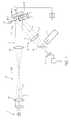
- FIG. 1is a diagrammatic illustration of a typical optical system, namely, a telescope, provided with an adaptive optics system that includes the deformable curvature mirror of the present invention
- FIG. 2is an enlarged, fragmentary sectional view through a portion of the deformable curvature mirror taken substantially on the line 2 — 2 in FIG. 1;
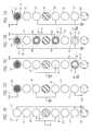
- FIGS. 3-6are elevation views of the rear side of the deformable curvature mirror of the present invention illustrating four different patterns of electrode segments.
- FIGS. 7A-7Eare diagrammatic views illustrating the layers of different materials that comprise various embodiments of the deformable curvature mirror of the present invention.
- an optical systemsuch as a telescope 10
- an adaptive optics systemthat includes the deformable curvature mirror 14 of the present invention.
- Light rays R from any light source Lsuch as the illustrated star when the telescope 10 is used for observing stars and planets, enter the telescope 10 through a lens 18 that focuses the light rays on an object image plane OIP where the image of the light source L (here a star, for example) exists in focus but is uncorrected.
- the telescope 10also may be of a type and construction for receiving light waves from an earth-bound data transmission station L, such as in a system for transmitting data from building-to-building, tower-to-tower, mountain-to-mountain or from ground to space.
- the light rays Rthen pass through a collimating lens 20 to the deformable mirror 14 of this invention.
- the light rays R reaching the telescope 10 from a distant star or other distant light source Lwould be undistorted and theoretically could produce a diffraction limited image of the source.
- the earth's atmospherecreates aberrations in the light rays R before reaching the telescope 10 , which aberrations vary with the atmospheric conditions and rapidly over any period of time, even when the telescope is located at high elevations.
- the telescope 10is used for viewing something on earth at a distance or for receiving light waves for data transmission from a station at a distance on earth, the earth's atmosphere will create aberrations in the light rays R and, therefore, produce a wavefront that can not produce a diffraction limited image and is constantly changing when it reaches the telescope 10 .
- Various wavefront sensorshave been used to detect the variations in the wavefront caused by the atmospheric aberrations and then to compensate or correct for those aberrations by adaptive optics, such as by using a deformable mirror controlled by a wavefront sensor.
- wavefront sensorthat is particularly suited for use with the deformable curvature mirror 14 of the present invention is a wavefront curvature sensor that uses a pair of defocused pupil images as described and shown in the copending U.S. patent application, Ser. No. 09/579,786, filed May 26, 2000 by the inventors hereof, which is incorporated herein by this reference.
- the light rays Rreflect from the surface of the deformable mirror 14 to a lens 22 that refocuses the image on the plane of an image detector D.
- the lens 18 , collimating lens 20 , deformable mirror 14 , lens 22 and image detector Dare all located and centered on the optical axis O of the system.
- the image detector Dmay be of any convenient type that is suitable for the particular application of the system, such as a conventional detector in a video camera, a custom format of charge couple device (CCD), an array of PIN diodes, an array of optical fibers, photon counting detectors, or the like.
- the detector Dprovides images and/or data relative to the light intensity throughout the image focused on detector D and these images and/or data are displayed and/or recorded on an appropriate device 24 suitable for this application of the system.
- the image appearing at the image detector Dwill be the uncorrected image received by telescope 10 .
- the image at detector Dwill be diffraction limited, i.e. a corrected image.
- the detector Dwill receive and detect corrected light rays when the deformable mirror 14 is properly deformed to correct for aberrations in the light rays R transmitted to the system illustrated in FIG. 1 . Still further, when such a system is used for transmitting data by light rays, the wavefront can be sensed and corrected by the deformable mirror 14 and the same mirror shape can be used to pre-correct a data light emitter positioned at the same location as image detector D.
- a partial mirror or beamsplitter 26is positioned on the optical axis O between lens 22 and detector D for reflecting a portion of the light rays R to a wavefront sensor S, such as one of the wavefront sensors disclosed in the inventors' copending patent application identified above.
- the wavefront sensor Ssenses two defocused pupil images (or the shapes and light intensities for some detectors used in a wavefront sensor S) which are communicated to the central processing unit CPU for processing by data reduction software to derive the wavefront curvature and provide data appropriate for the operation of the deformable mirror 14 .
- the wavefrontis derived or recovered by solving the Poisson equation with respect to intensities with the Dirichlet's boundary conditions relative to the shape of the extrafocal images.
- An iterative data reduction algorithm or other non-linear fitting techniquemay be employed to compensate for non-linearity in measurements in an open loop system.
- the CPUthen provides a plurality of separate and controlled high voltage electrical potentials to a plurality of conductive electrode segments (described below) on the back of deformable mirror 14 through a like plurality of separate wires W- 1 , W- 2 , W- 3 through W-N.
- the deformable mirror 14is fixedly mounted in a mount M that is appropriately positioned to reflect the optical axis O and light rays R from the collimating lens 20 to the detector D.
- the overall slope of the mirrori.e. the angle of reflection of the optical axis O, can be modified by the application of high voltages applied to selected electrode segments of the deformable mirror 14 through one or more of the wires W- 1 through W-N and the curvature of the surface of the deformable mirror 14 may be modified for correcting aberrations by the application of controlled high voltages also through wires W- 1 through W-N.
- FIG. 2a fragmentary and enlarged cross-section of a portion of the deformable curvature mirror 14 , taken on the line 2 — 2 in FIG. 1, is shown with the thicknesses of some of the layers of the laminated construction exaggerated for ease of illustration.
- the basic, physical structure of the deformable mirror 14is comprised of two discs or plates 30 and 32 of any electro-restrictive material that exhibits controlled expansion and contraction in response to the application of an electrical potential across the material and yet the material has an adequate structural strength and rigidity to maintain a given shape, as distinguished from being flexible.
- a preferred materialis ceramic PZT, which is a piezoelectric material comprised of Pb, Zu, Ti and O though a possible alternative is a magnetorestrictive material known as PMN comprised of Pb, Mg, Nb and O.
- the plates 30 and 32 of the electro-restrictive materialare separately ground to produce optically flat surfaces and a uniform thickness that depends on the size of the deformable mirror 14 but, in general, sufficiently thin to accommodate the flexures caused by the expansion and contraction induced by the electrical voltages.
- each of the PZT plates 30 and 32preferably would be less than two millimeters and more than 0.1 mm in thickness.
- each plate 30 and 32preferably would of a thickness between about 2.0 mm and 8.0 mm.
- a layer 34 of gold or other highly conductive material(hereinafter referred to as a gold layer for convenience) is applied to the lower surface of plate 30 and a gold layer 36 is applied to the upper surface of plate 32 and then the two plates 30 and 32 are laminated together and joined by a conductive adhesive 38 .
- the PZT plateshave a polarity in a direction perpendicular to the deformable mirror 14 which causes the PZT to expand when an electrical voltage is applied in one direction across the plate and to contract when the electrical voltage is applied in the opposite direction across the plate.
- each plate 30 and 32will exhibit a physical contraction in the direction perpendicular to the mirror 14 when an electric field created by the applied voltage with the positive potential on top and the negative potential on the bottom, as shown in FIG. 2 .
- any electric field traverses the lower PZT plate 32which is primarily inactive, the directions of expansion and contraction of the two plates 30 and 32 will be the same rather than tending to oppose each other.
- a plating mask(not shown) is applied to the outer surface 30 a to create a predetermined pattern, as described below, and then gold layers 40 and 42 are applied to the outer surfaces 30 a and 32 a , respectively, of the plates 30 and 32 .
- the mask and gold covering the mask on surface 30 aare removed to leave a pattern of gold electrodes 40 - 1 , 40 - 2 through 40 -N, only three of which are shown in the enlarged, fragmentary view of FIG. 2 .
- a mirror layer 48is applied to the outer surface 32 a of plate 32 by any convenient means such as epoxy replication wherein the mirror layer 48 is first formed separately and then adhered to the surface 32 a .
- Forming the mirror layer 42 by the epoxy replication methodincludes the steps of applying a mold separation material on a flat surface, applying a layer of reflective material, such as silver or gold, and then a layer of epoxy before adhering the mirror layer 48 to the gold layer 42 on the outer surface 32 a of plate 32 by an appropriate adhesive, such as epoxy, and curing the assembly at an elevated temperature.
- the outer surface of gold (or other metal) layer 42may be polished to a mirror-like condition, which may be adequate for some applications of the deformable mirror 14 .
- Electric terminals 44 - 1 , 44 - 2 through 44 -Nare attached to the electrode segments 40 - 1 through 40 -N by any convenient means, such as soldering.
- An insulating layer 46is then applied over the gold layer 40 (comprised of electrode segments 40 - 1 through 40 -N) and fills to gaps between the electrode segments formed by the mask material.
- the wires W- 1 through W-Nare attached to the terminals 44 - 1 through 44 -N, respectively.
- Electrical terminals and wiresare also attached to the intermediate gold layers 34 , 36 and the outer gold layer 42 by any convenient means, such as at the edge of the deformable mirror 14 or by drilling through the deformable mirror 14 near the periphery and installing one or more terminals and wires.
- the gold layers 34 , 36 , 42are all connected to ground and a positive voltage is applied to one or more of the wires W- 1 through W-N that an electric field will appear across electro-restrictive plate 30 to gold layer 34 from each electrode segment 40 - 1 through 40 -N to which the electrical potential has been applied and that some electric charge may flow through the conductive adhesive layer 38 to gold layer 36 establishing an electric field across plate 32 to grounded gold layer 42 .
- the electric fieldwill cause lateral expansion of the plate 30 and to a lesser degree the plate 32 .
- each electrode segment 40 - 1 through 40 -Nwill depend on the magnitude of the voltage applied to that electrode segment which expansion in turn causes the mirror 14 to deform in a controlled manner as a result of the electro-restrictive properties of the materials of the plates 30 and 32 .
- both sides of front plate 32have a gold layer which are electrically connected so that the front plate 32 and rear plate 30 mechanically behave in the same manner, such as with respect to thermal expansion and contraction, because the thermal expansion coefficient is controlled by grounding.
- the build-up of an electrical charge in PZT by temperature changes causing expansion and contractionwould store energy in the PZT and adversely effect the control of the curvature of the mirror surface 48 .
- FIGS. 3-6are plan views from the back, four typical patterns for the electrodes 40 on the deformable mirror 14 are shown with the terminals 44 - 1 , 44 -N omitted for clarity.
- each of the deformable mirrors 14 a , 14 b , 14 c and 14 d of FIGS. 3, 4 , 5 and 6 , respectively,is shown as being round and of the same size but it will readily appear to those skilled in the art that the deformable mirror 14 may be of a non-round shape for non-round adaptive optic systems, such as for lasers, and may be of different sizes, such as four different sizes of telescopes.
- the pattern of electrode segments 40 - 1 , 40 -N on the outer surface 30 a of plate 30is formed by the mask that is applied to the outer surface 30 a prior to applying the gold layer 40 , as described above.
- the mask for each of the deformable mirrors 14 a - 14 dincludes a perimeter portion to create a perimeter ring 30 b of exposed surface of the plate 30 , as well as the outer surface 32 a of plate 32 , for mounting the deformable mirror 14 in a supporting mount M (see FIG. 1 ). Thin strips of the masking material extend radially like spokes on the surface 30 a to form gaps 30 c between adjacent electrode segments 40 - 1 , 40 -N formed in circular rings, such as the outer rings 50 and inner rings 52 shown in FIGS.
- FIGS. 3, 4 and 5there are six electrode segments in the outer ring 50 and six electrode segments forming the inner ring 52
- there are eighteen electrode segments 44 in the outer ring 50twelve electrode segments in the inner ring 52 and six electrode segments 44 in the central ring 54 , but any number of electrode segments and separate rings may be used for a particular application.
- annular spaceis provided between the outer ring 50 and inner ring 52 of electrode segments, and the circular dashed line C in that annular space represents the outer diameter of the image received by the optical system, such as the outer diameter of the pupil image received by the telescope 10 .
- a dashed line C′ at the center of each mirror 14 in FIGS. 3-6represents the inner diameter of the pupil image of a reflective celestial telescope where no image appears inside of circle C′.
- the mirror layer 48may cover the entire portion of the surface of the deformable mirror 14 opposite the surface portion having the electrode patterns shown in FIGS.
- the image from the celestial telescopeis only reflected from the portions of the mirror between the outer diameter C and inner diameter C′.
- the imagewould cover the entire area within outer circle C with no inner blank space within the circle C′.
- the outer ring 50 of electrodescontrols the slope of the mirror by selectively applying voltages to each of the electrode segments 40 - 1 , 40 -N in the outer ring 50 to thereby tilt or change the slope of the whole mirror in any desired direction or amount, within the structural limits, for any desired purpose in connection with the adaptive optics system.
- the inner ring 52 of electrode segments, as well as the central ring 54 of electrode segments in FIG. 6,control the curvature of the mirror surface by applying appropriate voltages to each of the electrode segments.
- the gaps 30 c between electrode segmentsare large enough to insulate adjacent segments from each other but sufficiently small that the electric field passing through the plates 30 to the grounded layers 34 , 36 and 42 migrates and overlaps the segments to provide a smooth transition on the surface of the mirror layer 48 when different voltages are applied to adjacent electrode segments 40 - 1 , 40 -N.
- FIG. 3illustrates a basic electrode segment pattern with the functions and advantages thus far described and FIGS. 4-6 illustrate some modifications.
- an intermediate ring 56 of a layer of goldis formed in the annular space between the outer ring 50 and inner ring 52 of electrode segments as a modification to the embodiment illustrated in FIG. 3 .
- the intermediate ring 56is electrically grounded for preventing the build-up of an electrostatic charge on that portion of the surface 30 a of plate 30 that may be caused by expansion/contraction and movement of the plate 30 or, conversely, that may cause undesired expansion/contraction and movement of the plate 30 .
- the intermediate ring 56may be applied at the same time as the gold layer 40 by an appropriate shape of the same mask or may be applied in a subsequent plating step.
- an intermediate ring 56 ′is formed on the surface 30 a of plate 30 in the annular space between the outer ring 50 and inner ring 52 of electrode segments for the same purposes as intermediate ring 56 illustrated in FIG. 4 .
- Ring 56 ′is formed by separate circumferentially extending segments 58 , six being shown, with gaps formed between the segments 58 by the same mask during application of the gold layer 40 , which simplifies the construction of the mask by having connecting portions for the mask.
- connectors 60 of a conductive materialare applied between the segments 58 to connect them into a conductive ring 56 ′ which is grounded.
- An intermediate ring 56 ′′is also shown in FIG. 6 which may be of the type shown in FIG. 4 or FIG. 5 for the same purposes.
- the central ring 54 of electrode segmentsprovides additional control of the curvature of the mirror layer 48 even though a portion of those electrode segments are radially inward from the dashed-circle C′ representing the inner extremity of the image.
- these segments of the central ring 54would be important to controlling the curvature of that portion of the mirror layer 48 since an image would be reflected from that portion.
- FIGS. 7A-7Evarious embodiments of the different layers and different electrode patterns, as well as the electrical connections thereto, of the deformable curvature mirror 14 are diagrammatically illustrated.
- the electrode pattern layer 40is shown at the top of each Figure as one outer side of the deformable mirror 14 (omitting the terminals 44 - 1 , 44 -N and the insulation layer 46 that is coated on electrode layer 40 ) and the mirror surface layer 48 is shown at the bottom of each Figure as the other side of the deformable mirror 14 , with the layers therebetween illustrated in the order from top to bottom that is shown in FIG. 2 .
- the electro-restrictive plate 30immediately below the electrode layer 40 is the electro-restrictive plate 30 , then the gold layer 34 , then the adhesive layer 38 , then the gold layer 36 , then the electro-restrictive plate 32 , then the gold layer 42 and finally the mirror layer 48 .
- Some of the layersare illustrated with cross-hatching on their surfaces for distinguishing them with other layers but the cross-hatching is not intended to illustrate a sectional view through such layers.
- the electrode pattern layers 40 in FIGS. 7A-7Dare merely diagrammatic illustrations for showing the differences in the embodiments without necessarily illustrating electrode patterns that would be used commercially. Further, the mounting perimeter portions 30 b are omitted for simplicity and clarity. FIGS.
- FIG. 7A-7Ealso illustrate the electrical connections to the various conductive layers, namely, electrode segment layer 40 and gold layers 34 , 36 and 42 of the deformable mirror 14 with the letters “HV” indicating a variable high voltage to the entire layer or each of the individual electrode segments, although for simplicity of illustration only a single line to all of those segments is shown, such as electrode segment layer 40 in FIG. 7 A.
- the ground side of the electrical systemis indicated by either the electrical ground symbol, such as shown at the bottom left side of FIG. 7A or the letters “GND”.
- the gold layers 34 , 36 and 42are all connected to electrical ground as shown on the left side of FIG. 7 A.
- the plurality of electrode segments 40 - 1 through 40 -N of the electrode layer 40are individually connected to the controllable source of high voltage HV for selectively applying the desired voltage to each segment 40 - 1 , 40 -N for deforming the mirror.
- the electric fieldis applied across the electro-restrictive plate 30 to the grounded gold layer 34 .
- the single gold layer 34may be adequate to ground and conduct all of the electricity supplied from the electrode layer 40 , it is preferred that the additional electrical ground of gold layers 36 and 42 be provided to eliminate any possibility of any stray electricity or electrostatic charge affecting the second plate 32 in an uncontrolled manner in this embodiment.
- FIG. 7Ba different arrangement of the electrode segments for causing controlled deformation of the mirror 14 is shown wherein an outer ring of electrode segments 34 - 1 through 34 -N are provided in the gold layer 34 (rather than in gold layer 40 ), similar to the outer ring 50 of electrode segments described with respect to FIGS. 3-6 and an annular ring 62 of gold in layer 40 is grounded on the opposite side of plate 30 , whereby the slope of the mirror 14 may be controlled, at least in part, by applying the variable high voltages to the segments 34 - 1 through 34 -N so that the electric field is imposed across the electro-restrictive plate 30 to the ground ring 62 .
- the second intermediate gold layer 36is provided with an outer ring of electrode segments 36 - 1 through 36 -N that match and are superimposed on the electrode segments 34 - 1 through 34 -N, respectively, with the conductive adhesive layer therebetween, and an outer gold ring 64 is provided on the bottom of the other electro-restrictive plate 32 as a portion of gold layer 42 , which ring 64 is grounded whereby the electric field is imposed between electrode segments 36 - 1 , 36 -N of layer 36 through the plate 32 to the ground ring 64 .
- the layer 40is provided with electrode segments in the central portion comprised of, for example, an inner ring 52 , as shown in FIGS. 3-5, or both an inner ring 52 and a central ring 54 as shown in FIG.
- the gold layers 34 and 36are provided with central circles or discs 66 and 68 that are positioned opposite the inner ring and central ring of electrode segments of layer 40 to allow imposition of an electric field from those segments through the electro-restrictive first plate 30 for controlling the curvature of the mirror.
- the bottom gold layer 42is also provided with a central disc 70 opposite discs 66 and 68 which may be grounded for the same purposes described with respect to layer 42 in the embodiment of FIG. 7 A.
- disc 70may be connected to a high voltage source for applying a voltage across the electro-restrictive second plate 32 to the grounded discs 66 , 68 for causing a large and uniform deflection of the deformable mirror as an extra focus stroke in addition to the individual curvature deformations caused by the central electrode segments 40 - 1 through 40 -N.
- the mirror layer 48may be confined to a central portion approximating or smaller than the size of disc 70 to minimize the possibility of electrical arcing therethrough between ring 64 and disc 70 .
- This arrangement of FIG. 7Ballows for twice the stroke in the edge actuators compared to the arrangement of FIG. 7 A.
- both plates 30 and 32When a voltage is applied to one or more of the edge actuator segments 34 - 1 through 34 -N and 36 - 1 through 36 -N, both plates 30 and 32 will respond with an area of one expanding and a corresponding*superimposed) area of the other contracting to essentially double the bending movement.
- the individual electrode segments 34 - 1 through 34 -Nmay be electrically connected to the corresponding segments 36 - 1 through 36 -N by holes filled with conductive epoxy.
- the gold layer 40is provided with electrode segments 40 - 1 through 40 -N in the inner ring and/or central ring portions that are connected to the variable high voltage source for causing curvature changes in the deformable mirror 14 as in the embodiment of FIG. 7 B.
- the intermediate or center gold layers 34 and 36are grounded, as in the embodiment of FIG. 7 A.
- the bottom gold layer 42is provided with an outer ring of segments 42 - 1 through 42 -N, similar to the outer ring 50 of the embodiments shown in FIGS. 3-6, to which variable high voltages are applied for controlling the slope of the deformable mirror 14 .
- the upper gold layer 40is also provided with an outer ring of segments 40 - 1 through 40 -N that are positioned opposite the segments 42 - 1 through 42 -N, respectively.
- bottom gold layer 42is provided with a central disc 70 that may be grounded or connected to a second high. voltage source for providing the large and uniform deflection of the deformable mirror 14 for extra focus stroke, similar to the disc 70 of the embodiment of FIG. 7 B.
- the mirror layer 48may be limited to the central area of disk 70 to avoid arcing, as described above.
- This arrangement of FIG. 7Caccomplishes the same doubling of the stroke of edge actuators as the arrangement of FIG. 7B but the electrical connections the edge electrode segments is easier.
- FIG. 7Danother embodiment of the arrangement of the electrode segments and ground layers is illustrated wherein the upper gold layer 40 and central gold layers 34 and 36 may be substantially the same as the embodiment of FIG. 7A wherein both the slope and the curvature of the mirror 14 are controlled by electrode segments provided in outer, inner and central rings of electrode segments 40 - 1 through 40 -N of the gold layer 40 and layers 34 and 36 are grounded.
- the bottom gold layer 42may be connected to a second high voltage source (rather than ground, as in FIG.
- FIG. 7Eanother embodiment of the deformable mirror 14 having different uses than the previously described deformable mirrors of this invention is diagrammatically illustrated.
- An upper gold layer 72is a single circle or disc rather than having a plurality of electrode segments 40 - 1 through 40 -N, as in the upper gold layer 40 of the previously described embodiments.
- This embodiment of FIG. 7Eincludes, in order from the upper layer 72 downward, the electro-restrictive plate 30 , the gold layer 34 , the conductive adhesive layer 38 , the gold layer 36 , the electro-restrictive plate 32 , the bottom gold layer 42 and the mirror layer 48 which may be constructed in substantially the same manner as described with respect to FIG. 2 .
- the 7Ehas the two central gold layers 34 and 36 connected to a variable high voltage source and the upper gold layer 72 and lower gold layer 42 connected to ground, as illustrated.
- the entire deformable mirror 14 awill be deformed to form a concave surface on the mirror layer 48 whereby the deformable mirror 14 a may be used to change the focal length of an image reflected from mirror layer 48 .
- the polarity of the electro-restrictive plates 30 , 32are reversed rather than being aligned because the electric fields therethrough are reversed and thus the deformation is additive.
- This form of deformable mirroris useful in conjugate tuning of an optical system, as distinguished from wavefront correction in the adaptive optics system, which may be useful in conjunction with a wavefront sensor for conjugate tuning in a data transmission system using light waves.
- the polarity of the applied electrical potentialmay be reversed, that is, the central gold layers 34 , 36 may be grounded and the outer gold layers 72 , 42 may be used for applying the variable high voltage for varying the focal length of the deformable mirror 14 e.
- deformable mirrors 14 described in detail with respect to FIGS. 2-6 and 7 A- 7 D and innumerable variations thereofmay be used in the optical system of FIG. 1 or any other optical system that is susceptible to adaptive optics for correcting a light wavefront by using the deformable mirror 14 of the present invention.
- the wavefront sensor SAs the light rays R that are reflected by the deformable mirror 14 and received by the wavefront sensor S, which through the CPU applies the appropriate high voltages HV to the respective electrode segments 40 - 1 through 40 -N (or 34 - 1 through 34 -N or 36 - 1 through 36 -N or 42 - 1 through 42 -N in the various embodiments), the slope and curvature of the mirror layer 48 of the mirror 14 are modified continually and instantaneously until the wavefront sensor senses a flat wavefront, as corrected by the deformable mirror 14 in a continuing feedback arrangement, whereby a diffraction limited images is observed at detector D.
- the wavefront sensor Swhich causes the curvature and/or slope of the deformable mirror 14 to be modified for correcting the change in the wavefront to assure that the wavefront reaching the detector D is continually corrected.
- the optical system of FIG. 1 or any similar optical system having an adaptive optics arrangement using the deformable curvature mirror 14may be calibrated by introducing a controlled light source so that the wavefront sensor S may detect whether the mirror layer 48 of the deformable mirror 14 is providing a diffraction limited image and, if not, such as by reason of manufacturing defects or the like, the wavefront sensor S and CPU can apply appropriate high voltages to the electrode segments of the deformable mirror for correcting the mirror to an optically correct condition.
- the deformable mirror of the present inventionhas been described in connection with a specific optical system, namely, the telescope illustrated in FIG. 1, it will readily appear to those skilled in the art that the deformable mirror may be used in any optical system in which adaptive optics for correcting the wavefront may be useful, and that numerous variations and modifications of the precise construction of the deformable mirror and the arrangement of the pattern of the electrode segments, in addition to those disclosed herein, may be made without departing from the invention as hereinafter claimed.
Landscapes
- Physics & Mathematics (AREA)
- General Physics & Mathematics (AREA)
- Optics & Photonics (AREA)
- Nonlinear Science (AREA)
- Optical Elements Other Than Lenses (AREA)
- Mechanical Light Control Or Optical Switches (AREA)
Abstract
Description
Claims (40)
Priority Applications (7)
| Application Number | Priority Date | Filing Date | Title |
|---|---|---|---|
| US09/769,988US6464364B2 (en) | 2000-01-27 | 2001-01-25 | Deformable curvature mirror |
| IL15710002AIL157100A0 (en) | 2001-01-25 | 2002-01-22 | Deformable curvature mirror |
| EP02709289AEP1364244B1 (en) | 2001-01-25 | 2002-01-22 | Deformable curvature mirror |
| JP2002559738AJP2004523785A (en) | 2001-01-25 | 2002-01-22 | Deformable curved mirror |
| CNB02806268XACN1280652C (en) | 2001-01-25 | 2002-01-22 | deformable mirror |
| PCT/US2002/003048WO2002059674A1 (en) | 2001-01-25 | 2002-01-22 | Deformable curvature mirror |
| US10/266,981US6874897B2 (en) | 2000-01-27 | 2002-10-08 | Deformable curvature mirror with unipolar-wiring |
Applications Claiming Priority (2)
| Application Number | Priority Date | Filing Date | Title |
|---|---|---|---|
| US17841600P | 2000-01-27 | 2000-01-27 | |
| US09/769,988US6464364B2 (en) | 2000-01-27 | 2001-01-25 | Deformable curvature mirror |
Related Child Applications (1)
| Application Number | Title | Priority Date | Filing Date |
|---|---|---|---|
| US10/266,981Continuation-In-PartUS6874897B2 (en) | 2000-01-27 | 2002-10-08 | Deformable curvature mirror with unipolar-wiring |
Publications (2)
| Publication Number | Publication Date |
|---|---|
| US20010040743A1 US20010040743A1 (en) | 2001-11-15 |
| US6464364B2true US6464364B2 (en) | 2002-10-15 |
Family
ID=25087128
Family Applications (1)
| Application Number | Title | Priority Date | Filing Date |
|---|---|---|---|
| US09/769,988Expired - LifetimeUS6464364B2 (en) | 2000-01-27 | 2001-01-25 | Deformable curvature mirror |
Country Status (6)
| Country | Link |
|---|---|
| US (1) | US6464364B2 (en) |
| EP (1) | EP1364244B1 (en) |
| JP (1) | JP2004523785A (en) |
| CN (1) | CN1280652C (en) |
| IL (1) | IL157100A0 (en) |
| WO (1) | WO2002059674A1 (en) |
Cited By (24)
| Publication number | Priority date | Publication date | Assignee | Title |
|---|---|---|---|---|
| US20030107828A1 (en)* | 2000-01-27 | 2003-06-12 | Graves J. Elon | Deformable curvature mirror with unipolar wiring |
| US6721510B2 (en) | 2001-06-26 | 2004-04-13 | Aoptix Technologies, Inc. | Atmospheric optical data transmission system |
| US20040141752A1 (en)* | 2003-01-16 | 2004-07-22 | Shelton J. Christopher | Free space optical communication system with power level management |
| US20040201908A1 (en)* | 2002-10-16 | 2004-10-14 | Olympus Corporation | Variable-shape reflection mirror and method of manufacturing the same |
| US20050069324A1 (en)* | 2003-09-29 | 2005-03-31 | Harris Corporation | Free space optical (FSO) device providing remote control features and related methods |
| US20050069323A1 (en)* | 2003-09-29 | 2005-03-31 | Harris Corporation, Corporation Of The State Of Delaware | Modular free space optical (FSO) device and related methods |
| US20050069322A1 (en)* | 2003-09-29 | 2005-03-31 | Harris Corporation | Free space optical (FSO) device providing power reduction features and related methods |
| US20050180753A1 (en)* | 2004-02-12 | 2005-08-18 | Adaptive Optics Associates, Inc. | Free space optical (FSO) laser communication system employing fade mitigation measures based on laser beam speckle tracking and locking principles |
| US20060024061A1 (en)* | 2004-02-12 | 2006-02-02 | Adaptive Optics Associates, Inc. | Wavefront sensing system employing active updating of reference positions and subaperture locations on wavefront sensor |
| US7019888B1 (en)* | 2002-10-17 | 2006-03-28 | Aoptix Technologies | Deformable mirror with perimeter wiring |
| US20060140454A1 (en)* | 2004-12-07 | 2006-06-29 | Northcott Malcolm J | Iris imaging using reflection from the eye |
| US20070035855A1 (en)* | 2003-03-03 | 2007-02-15 | Dickensheets David L | Miniature confocal optical device, system, and method |
| US20070216798A1 (en)* | 2004-12-07 | 2007-09-20 | Aoptix Technologies, Inc. | Post processing of iris images to increase image quality |
| US20070223929A1 (en)* | 2005-03-23 | 2007-09-27 | Graves J E | Data port alignment of free space optical communications terminal with adaptive optics |
| WO2007113296A1 (en) | 2006-04-03 | 2007-10-11 | Vodafone Holding Gmbh | Measurement data recording |
| US7289736B1 (en) | 2003-01-13 | 2007-10-30 | Aoptix Technologies | Adaptive optics imaging system with object acquisition capability |
| US20070280609A1 (en)* | 2006-05-23 | 2007-12-06 | Canon Kabushiki Kaisha | Optical element driving apparatus |
| US7418115B2 (en) | 2004-12-07 | 2008-08-26 | Aoptix Technologies, Inc. | Iris imaging using reflection from the eye |
| US20100027142A1 (en)* | 2007-11-02 | 2010-02-04 | The United States Of America As Represented By The Secretary Of The Army | Scalable-Size Deformable Pocket Mirror With On-Pocket Bimorph Actuator |
| US7689127B1 (en)* | 2004-04-15 | 2010-03-30 | Lockheed Martin Corporation | Deformable mirrors for multi-access laser communications terminal |
| US20100172649A1 (en)* | 2009-01-07 | 2010-07-08 | Graves J Elon | Free-Space Optical Transceiver Using Multimode Fiber to Couple Single Mode Input Optical Signal |
| US8092021B1 (en) | 2007-01-26 | 2012-01-10 | Aoptix Technologies, Inc. | On-axis illumination for iris imaging |
| US8132912B1 (en)* | 2008-06-29 | 2012-03-13 | Aoptix Technologies, Inc. | Iris imaging system using circular deformable mirror mounted by its circumference |
| US9450670B1 (en)* | 2014-07-31 | 2016-09-20 | Aoptix Technologies, Inc. | Position sensor for a fast steering mirror |
Families Citing this family (31)
| Publication number | Priority date | Publication date | Assignee | Title |
|---|---|---|---|---|
| GB0204603D0 (en)* | 2002-02-27 | 2002-04-10 | Univ Sussex The | Pattern recognition system |
| US6989922B2 (en)* | 2002-06-21 | 2006-01-24 | Nikon Corporation | Deformable mirror actuation system |
| JP2006512607A (en)* | 2002-12-30 | 2006-04-13 | コーニンクレッカ フィリップス エレクトロニクス エヌ ヴィ | Optical device including a polymer actuator |
| WO2005024809A2 (en)* | 2003-09-04 | 2005-03-17 | Matsushita Electric Industrial Co., Ltd. | Optical pick-up aberration correcting mirror, aberration correcting method and optical pick-up |
| DE102004011026A1 (en)* | 2004-03-04 | 2005-09-29 | Siemens Ag | Adaptive optical element with a polymer actuator |
| US7567374B2 (en) | 2004-06-22 | 2009-07-28 | Bae Systems Plc | Deformable mirrors |
| WO2006032878A1 (en)* | 2004-09-21 | 2006-03-30 | Mbda Uk Limited | Adaptive-optics method and apparatus |
| JP2006154765A (en)* | 2004-10-27 | 2006-06-15 | Matsushita Electric Ind Co Ltd | Mirror element and mirror array |
| DE102005044716A1 (en)* | 2005-09-19 | 2007-04-05 | Carl Zeiss Smt Ag | Active optical element |
| JP2008097683A (en)* | 2006-10-10 | 2008-04-24 | Funai Electric Co Ltd | Deformable mirror and optical pickup device having the same |
| US7473878B2 (en)* | 2007-06-08 | 2009-01-06 | The Boeing Company | High power bimorph wave-front correction mirror |
| CN100485330C (en)* | 2007-06-18 | 2009-05-06 | 中国科学院西安光学精密机械研究所 | An Imaging Spectrum Measuring Device |
| JP5632748B2 (en)* | 2008-02-05 | 2014-11-26 | コーニンクレッカ フィリップス エヌ ヴェ | Illumination device comprising a reflective electroactive polymer actuator |
| US8659835B2 (en) | 2009-03-13 | 2014-02-25 | Optotune Ag | Lens systems and method |
| US8699141B2 (en) | 2009-03-13 | 2014-04-15 | Knowles Electronics, Llc | Lens assembly apparatus and method |
| US9383576B2 (en)* | 2012-07-17 | 2016-07-05 | Rachel Andreasen | Apparatus and method for a flexible adaptive telescope mirror |
| CN103345059B (en)* | 2013-06-28 | 2015-07-15 | 中国科学院西安光学精密机械研究所 | Method and system for zooming of reflective deformable mirror |
| DE102015213275A1 (en)* | 2015-07-15 | 2017-01-19 | Carl Zeiss Smt Gmbh | Mirror assembly for a lithographic exposure system and mirror assembly comprehensive optical system |
| WO2017195163A1 (en)* | 2016-05-13 | 2017-11-16 | Ecole Polytechnique Federale De Lausanne (Epfl) | System, method and apparatus for retinal absorption phase and dark field imaging with oblique illumination |
| IT201600070259A1 (en)* | 2016-07-06 | 2018-01-06 | Adige Spa | Process of laser processing of a metal material with control of the position of the optical axis of the laser with respect to a flow of assistance gas, as well as a machine and computer program for carrying out such a process. |
| IT201600070441A1 (en)* | 2016-07-06 | 2018-01-06 | Adige Spa | Process for laser processing of a metal material with high-dynamic control of the axes of movement of the laser beam along a predetermined processing path, as well as a machine and computer program for carrying out such a process. |
| DE102017205405A1 (en)* | 2017-03-30 | 2018-10-04 | Carl Zeiss Smt Gmbh | Mirror, in particular for a microlithographic projection exposure apparatus |
| JP6737220B2 (en)* | 2017-03-31 | 2020-08-05 | 株式会社デンソー | Varifocal mirror |
| CN108458816B (en)* | 2018-03-09 | 2020-06-23 | 业成科技(成都)有限公司 | Curved surface electrode structure |
| CN108627972A (en)* | 2018-04-20 | 2018-10-09 | 中国人民解放军国防科技大学 | Cantilever type transverse piezoelectric driven deformable mirror and its assembly method |
| US11899336B2 (en)* | 2019-04-19 | 2024-02-13 | Osaka University | Liquid crystal element |
| US11442332B1 (en)* | 2020-10-26 | 2022-09-13 | Amazon Technologies, Inc. | Tunable liquid crystal lens with electrically tunable axis of astigmatism |
| JPWO2023277047A1 (en)* | 2021-07-02 | 2023-01-05 | ||
| WO2023048964A1 (en)* | 2021-09-23 | 2023-03-30 | Corning Incorporated | Method and apparatus for applying light to cure adhesives |
| US12066738B2 (en)* | 2022-09-01 | 2024-08-20 | Meta Platforms Technologies, Llc | Gradient-index liquid crystal lens having lens segments with optical power gradient |
| US11733547B1 (en)* | 2022-09-27 | 2023-08-22 | Pixieray Oy | Modulating impedance to segments of ground plane |
Citations (14)
| Publication number | Priority date | Publication date | Assignee | Title |
|---|---|---|---|---|
| FR2389143A1 (en)* | 1977-04-27 | 1978-11-24 | Quantel Sa | Piezoelectric variable mirror or lens - of laminated structure including two piezoelectric ceramic layers |
| US4128309A (en)* | 1975-08-19 | 1978-12-05 | Thomson-Brandt | Automatic optical focusing device |
| US4257686A (en)* | 1978-12-14 | 1981-03-24 | Itek Corporation | Multiple layer piezoelectric wavefront modulator |
| US4298247A (en)* | 1979-04-04 | 1981-11-03 | Quantel S.A. | Thick optical element having a variable curvature |
| US4420222A (en)* | 1978-04-13 | 1983-12-13 | Quantel S.A. | Mirror having a variable focal length |
| US4588268A (en)* | 1984-03-12 | 1986-05-13 | Itek Corporation | Tip-tilt mirror actuation system having simplified driver circuitry |
| GB2247323A (en)* | 1990-07-20 | 1992-02-26 | Andreas Theodoros Augousti | Variable shape telescopic mirror |
| US5262696A (en)* | 1991-07-05 | 1993-11-16 | Rockwell International Corporation | Biaxial transducer |
| US5329322A (en) | 1992-05-26 | 1994-07-12 | Yancey Don R | Palm size autorefractor and fundus topographical mapping instrument |
| US5576780A (en) | 1992-05-26 | 1996-11-19 | Cain Research Pty. Ltd. | Method for evaluation of length of focus of the eye |
| WO1997012267A1 (en)* | 1996-10-17 | 1997-04-03 | Yalestown Corporation N.V. | Deformable mirror based on a multilayered active bimorph structure |
| US5777719A (en) | 1996-12-23 | 1998-07-07 | University Of Rochester | Method and apparatus for improving vision and the resolution of retinal images |
| US5907153A (en)* | 1996-12-09 | 1999-05-25 | Fujifilm Electronic Imaging Ltd. | Radiation beam scanning apparatus and method employing distortion compensation |
| US6023057A (en) | 1996-10-31 | 2000-02-08 | Compagnie Industrielle Des Lasers Cilas | Device for determining the phase errors of electromagnetic waves |
- 2001
- 2001-01-25USUS09/769,988patent/US6464364B2/ennot_activeExpired - Lifetime
- 2002
- 2002-01-22JPJP2002559738Apatent/JP2004523785A/enactivePending
- 2002-01-22ILIL15710002Apatent/IL157100A0/enactiveIP Right Grant
- 2002-01-22CNCNB02806268XApatent/CN1280652C/ennot_activeExpired - Fee Related
- 2002-01-22EPEP02709289Apatent/EP1364244B1/ennot_activeExpired - Lifetime
- 2002-01-22WOPCT/US2002/003048patent/WO2002059674A1/enactiveApplication Filing
Patent Citations (15)
| Publication number | Priority date | Publication date | Assignee | Title |
|---|---|---|---|---|
| US4128309A (en)* | 1975-08-19 | 1978-12-05 | Thomson-Brandt | Automatic optical focusing device |
| FR2389143A1 (en)* | 1977-04-27 | 1978-11-24 | Quantel Sa | Piezoelectric variable mirror or lens - of laminated structure including two piezoelectric ceramic layers |
| US4420222A (en)* | 1978-04-13 | 1983-12-13 | Quantel S.A. | Mirror having a variable focal length |
| US4257686A (en)* | 1978-12-14 | 1981-03-24 | Itek Corporation | Multiple layer piezoelectric wavefront modulator |
| US4298247A (en)* | 1979-04-04 | 1981-11-03 | Quantel S.A. | Thick optical element having a variable curvature |
| US4588268A (en)* | 1984-03-12 | 1986-05-13 | Itek Corporation | Tip-tilt mirror actuation system having simplified driver circuitry |
| GB2247323A (en)* | 1990-07-20 | 1992-02-26 | Andreas Theodoros Augousti | Variable shape telescopic mirror |
| US5262696A (en)* | 1991-07-05 | 1993-11-16 | Rockwell International Corporation | Biaxial transducer |
| US5329322A (en) | 1992-05-26 | 1994-07-12 | Yancey Don R | Palm size autorefractor and fundus topographical mapping instrument |
| US5576780A (en) | 1992-05-26 | 1996-11-19 | Cain Research Pty. Ltd. | Method for evaluation of length of focus of the eye |
| WO1997012267A1 (en)* | 1996-10-17 | 1997-04-03 | Yalestown Corporation N.V. | Deformable mirror based on a multilayered active bimorph structure |
| US6023057A (en) | 1996-10-31 | 2000-02-08 | Compagnie Industrielle Des Lasers Cilas | Device for determining the phase errors of electromagnetic waves |
| US5907153A (en)* | 1996-12-09 | 1999-05-25 | Fujifilm Electronic Imaging Ltd. | Radiation beam scanning apparatus and method employing distortion compensation |
| US5777719A (en) | 1996-12-23 | 1998-07-07 | University Of Rochester | Method and apparatus for improving vision and the resolution of retinal images |
| US5949521A (en) | 1996-12-23 | 1999-09-07 | University Of Rochester | Method and apparatus for improving vision and the resolution of retinal images |
Non-Patent Citations (24)
| Title |
|---|
| A. Chellabi, et al., "A New Control Algorithm for Bimorph MIrrors", Systems, Man, and Cybernetics, 1995. Intelligent Systems for the 21st Century. IEEE Conf. on, vol. 1, 1995, pp. 569-573.** |
| Andrey G. Safronńov, "Bimorph Piezoelectric Structures in Laser and Astronomic Adaptive Optics", Conference on Lasers and Electro-optics, Europe 1996 (CLEO/Europe 1996), Tuesday/1991, CTuK4.** |
| Erez N. Ribak, "Deformable Mirrors", Adaptive Optics for Astronomy, D.M. Alloin and J. M. Mariotti (eds.), Kluwer Academic Publishers, Netherlands, pp. 149-162, 1994.** |
| Hua Wei Zhou, et al., "Prototype Bimorph Mirror for the AAT Adaptive Optics System", SPIE vol. 3126 (Adaptive Optics and Applications), pp. 384-391, 1997.** |
| J.E. Graves, et al., "Latest Results from the University of Hawaii Prototype Adaptive Optics System", Univ. Hawaii Laser Guide Star Adaptive Optics Workshop: Proceedings-vol. 1 (Mar. 10-12, 1992), pp 511-521. |
| Proceedings of SPIE 3353, Mar. 1998 entitled First Light For Hokupa'a; Author Graves et al. |
| Publication entitled "A Simple Low-Order Adaptive Optics System For Near-Infrared Applications"; Publications of the Astronomical Society of the Pacific; vol. 103, Jan. 1991, No. 659 by Roddier et al. pp 131-149. |
| Publication entitled "A Subjective Method for the Measurement of Monochromatic Aberrations of the Eye", J. Opt Soc. Am 1977; 67(11): 1508-1518 by Howland HC et al. |
| Publication entitled "Active Optical Depth Resolution Improvement of the Laser Tomographic Scanner"; Applied Optics, vol. 28, No. 4, pp. 804-808, (1989) by Dreher et al. |
| Publication entitled "Computing High order Wave Aberration Coefficients from Small Variations of Best Focus for Small Artificial Pupils"; Vision Res. 1989; 29(8); 979-83 by Howland HC et al. |
| Publication entitled "Curvature Sensing and Compensation: A New concept in Adaptive Optics"; applied Optics, vol. 27, pp. 1223-1225, by Roddier F. Apr. 1, 1988. |
| Publication entitled "Measurement of Monochromatic Ocular Aberrations of human Eyes as a Function of Accommodation by the Howland Aberroscope Technique"; Vision Res. 1995: 35(3): 313-23 by Atchinson DA et al. |
| Publication entitled "Measurement of the Axial Wavefront Aberration of the Human Eye", Opthal Physiol Opt. 1985; 5: 23-31 by Walsh, G. et al. |
| Publication entitled "Measurement of the Wave Aberration of the Human Eye"; Biophysics 1961; 6: 776-94; by Smirnov MS (Translated). |
| Publication entitled "New Optical Testing methods Developed at the University of Hawaii; Results of Ground-Based Telescopes and Hubble Space Telescope"; SPIE, vol. 1531, pp. 37-43, 1991 by Roddier C. et al. |
| Publication entitled "Objective Measurement of Wave Aberrations of the Human Eye with the Use of a Hartmann-Shack Wave-Front Sensor", J. Opt. Soc. Am. A., vol. 11, No. 7, Jul. 1994; Authors Liang et al. pp 1949-1957. |
| Publication entitled "Objective Technique for the Determination of Monochromatic Aberrations of the Human Eye", J. opt. Soc. Am. A., vol. 1, No. 9, pp. 987-992 (1984) by Walsh et al. |
| Publication entitled "Reliability and Validity Studies of a New Computer-Assisted Crossed-Cylinder Aberroscope"; Optom Vis. Sci. 1997; 74(7): 570-80 by Cox MJ et al. |
| Publication entitled "Retrieval of Wave Aberration of Human Eyes from Actual Point-Spread Function Data"; J. Opt Soc. Am 1988; 5(8); 1201-6 by Artal P. et al. |
| Publication entitled "Scanning Laser Tomography of the Living Human Eye" in Noninvasive Diagnostic Techniques in Ophthalmology. Masters BR (ed.), Springer-Verlag, pp. 528-547 (1990); Authors Bille et al. |
| Publication entitled "Subjective Measurement of High-Order Aberrations of the Eye", Science 1976; 193: 580-2 by Howland B. et al. |
| Publication entitled "Wavefront Aberration of the Eye: A Review"; Optometry and Vision Science 1991; 68(8): 574-583 by Charman WN. |
| Publication entitled "Wavefront Determination Resulting From Foucault Tests Applied to the Human Eye and Visual Instruments"; In Optical instruments and Techniques, Dickson JH (ed.), London, Oriel, 1969, 375-85. |
| Publication entitled "Wavefront Sensing and the Irradiance Transport Equation"; Applied Optics, vol. 29 (10), pp. 1402-1403, 1990 by Roddier F. |
Cited By (41)
| Publication number | Priority date | Publication date | Assignee | Title |
|---|---|---|---|---|
| US20030107828A1 (en)* | 2000-01-27 | 2003-06-12 | Graves J. Elon | Deformable curvature mirror with unipolar wiring |
| US6874897B2 (en) | 2000-01-27 | 2005-04-05 | Aoptix Technologies, Inc. | Deformable curvature mirror with unipolar-wiring |
| US6721510B2 (en) | 2001-06-26 | 2004-04-13 | Aoptix Technologies, Inc. | Atmospheric optical data transmission system |
| US20040156638A1 (en)* | 2001-06-26 | 2004-08-12 | Graves J. Elon | Atmospheric optical data transmission system |
| US6986587B2 (en)* | 2002-10-16 | 2006-01-17 | Olympus Corporation | Variable-shape reflection mirror and method of manufacturing the same |
| US20040201908A1 (en)* | 2002-10-16 | 2004-10-14 | Olympus Corporation | Variable-shape reflection mirror and method of manufacturing the same |
| US7019888B1 (en)* | 2002-10-17 | 2006-03-28 | Aoptix Technologies | Deformable mirror with perimeter wiring |
| US7289736B1 (en) | 2003-01-13 | 2007-10-30 | Aoptix Technologies | Adaptive optics imaging system with object acquisition capability |
| US20040141752A1 (en)* | 2003-01-16 | 2004-07-22 | Shelton J. Christopher | Free space optical communication system with power level management |
| US7286766B2 (en) | 2003-01-16 | 2007-10-23 | Aoptix Technologies, Inc. | Free space optical communication system with power level management |
| US20070035855A1 (en)* | 2003-03-03 | 2007-02-15 | Dickensheets David L | Miniature confocal optical device, system, and method |
| US7272322B2 (en) | 2003-09-29 | 2007-09-18 | Harris Corporation | Modular free space optical (FSO) device and related methods |
| US7215890B2 (en) | 2003-09-29 | 2007-05-08 | Harris Corporation | Free space optical (FSO) device providing power reduction features and related methods |
| US7221874B2 (en) | 2003-09-29 | 2007-05-22 | Harris Corporation | Free space optical (FSO) device providing remote control features and related methods |
| US20050069322A1 (en)* | 2003-09-29 | 2005-03-31 | Harris Corporation | Free space optical (FSO) device providing power reduction features and related methods |
| US20050069323A1 (en)* | 2003-09-29 | 2005-03-31 | Harris Corporation, Corporation Of The State Of Delaware | Modular free space optical (FSO) device and related methods |
| US20050069324A1 (en)* | 2003-09-29 | 2005-03-31 | Harris Corporation | Free space optical (FSO) device providing remote control features and related methods |
| US20060024061A1 (en)* | 2004-02-12 | 2006-02-02 | Adaptive Optics Associates, Inc. | Wavefront sensing system employing active updating of reference positions and subaperture locations on wavefront sensor |
| US20050196166A1 (en)* | 2004-02-12 | 2005-09-08 | Adaptive Optics Associates, Inc. | Wavefront sensing system employing active updating of reference positions and subaperture locations on wavefront sensor |
| US7457545B2 (en) | 2004-02-12 | 2008-11-25 | Northrop Grumman Corporation | Process for controlling a Hartmann wavefront sensor (WFS) in an adaptive optic (AO) system |
| US20050180753A1 (en)* | 2004-02-12 | 2005-08-18 | Adaptive Optics Associates, Inc. | Free space optical (FSO) laser communication system employing fade mitigation measures based on laser beam speckle tracking and locking principles |
| US7437077B2 (en) | 2004-02-12 | 2008-10-14 | Northrop Grumman Corporation | Wavefront sensing system employing active updating of reference positions and subaperture locations on wavefront sensor |
| US7343099B2 (en) | 2004-02-12 | 2008-03-11 | Metrologic Instruments, Inc. | Free space optical (FSO) laser communication system employing fade mitigation measures based on laser beam speckle tracking and locking principles |
| US7689127B1 (en)* | 2004-04-15 | 2010-03-30 | Lockheed Martin Corporation | Deformable mirrors for multi-access laser communications terminal |
| US20060140454A1 (en)* | 2004-12-07 | 2006-06-29 | Northcott Malcolm J | Iris imaging using reflection from the eye |
| US7869627B2 (en) | 2004-12-07 | 2011-01-11 | Aoptix Technologies, Inc. | Post processing of iris images to increase image quality |
| US7418115B2 (en) | 2004-12-07 | 2008-08-26 | Aoptix Technologies, Inc. | Iris imaging using reflection from the eye |
| US7428320B2 (en) | 2004-12-07 | 2008-09-23 | Aoptix Technologies, Inc. | Iris imaging using reflection from the eye |
| US20070216798A1 (en)* | 2004-12-07 | 2007-09-20 | Aoptix Technologies, Inc. | Post processing of iris images to increase image quality |
| US20070223929A1 (en)* | 2005-03-23 | 2007-09-27 | Graves J E | Data port alignment of free space optical communications terminal with adaptive optics |
| US7616897B2 (en) | 2005-03-23 | 2009-11-10 | Aoptix Technologies, Inc. | Data port alignment of free space optical communications terminal with adaptive optics |
| WO2007113296A1 (en) | 2006-04-03 | 2007-10-11 | Vodafone Holding Gmbh | Measurement data recording |
| US20070280609A1 (en)* | 2006-05-23 | 2007-12-06 | Canon Kabushiki Kaisha | Optical element driving apparatus |
| US7710626B2 (en)* | 2006-05-23 | 2010-05-04 | Canon Kabushiki Kaisha | Optical element driving apparatus |
| US8092021B1 (en) | 2007-01-26 | 2012-01-10 | Aoptix Technologies, Inc. | On-axis illumination for iris imaging |
| US20100027142A1 (en)* | 2007-11-02 | 2010-02-04 | The United States Of America As Represented By The Secretary Of The Army | Scalable-Size Deformable Pocket Mirror With On-Pocket Bimorph Actuator |
| US7967456B2 (en) | 2007-11-02 | 2011-06-28 | The United States Of America As Represented By The Secretary Of The Army | Scalable size deformable pocket mirror with on-pocket bimorph actuator |
| US8132912B1 (en)* | 2008-06-29 | 2012-03-13 | Aoptix Technologies, Inc. | Iris imaging system using circular deformable mirror mounted by its circumference |
| US20100172649A1 (en)* | 2009-01-07 | 2010-07-08 | Graves J Elon | Free-Space Optical Transceiver Using Multimode Fiber to Couple Single Mode Input Optical Signal |
| US8260146B2 (en) | 2009-01-07 | 2012-09-04 | Aoptix Technologies, Inc. | Free-space optical transceiver using multimode fiber to couple single mode input optical signal |
| US9450670B1 (en)* | 2014-07-31 | 2016-09-20 | Aoptix Technologies, Inc. | Position sensor for a fast steering mirror |
Also Published As
| Publication number | Publication date |
|---|---|
| IL157100A0 (en) | 2004-02-08 |
| JP2004523785A (en) | 2004-08-05 |
| EP1364244A1 (en) | 2003-11-26 |
| EP1364244B1 (en) | 2012-12-05 |
| CN1280652C (en) | 2006-10-18 |
| EP1364244A4 (en) | 2009-09-16 |
| CN1496489A (en) | 2004-05-12 |
| WO2002059674A1 (en) | 2002-08-01 |
| US20010040743A1 (en) | 2001-11-15 |
Similar Documents
| Publication | Publication Date | Title |
|---|---|---|
| US6464364B2 (en) | Deformable curvature mirror | |
| US6568647B2 (en) | Mounting apparatus for a deformable mirror | |
| US4093351A (en) | Controlled flexible membrane reflector | |
| US7294282B1 (en) | Method for fabricating an actuator system | |
| US7098871B1 (en) | Optical scanning system with correction | |
| RU2084941C1 (en) | Adaptive optical module | |
| US6800988B1 (en) | Voltage and light induced strains in porous crystalline materials and uses thereof | |
| JP3165444B2 (en) | M × N thin-film actuated mirror array and method of manufacturing the same | |
| US20020109894A1 (en) | Vertical comb drive actuated deformable mirror device and method | |
| US20060103956A1 (en) | Deformable mirror | |
| US4280756A (en) | Piezoelectric bi-morph mirror actuator | |
| RU2125347C1 (en) | Array of thin-film controlled reflectors for optical projection system and its manufacturing process | |
| KR20160016801A (en) | Optical structure on which connecting pieces are mounted and method for producing said optical structure | |
| US8570637B2 (en) | Micromechanical element | |
| KR101891652B1 (en) | Optical structure having webs arranged thereon and method for the production of same | |
| US6874897B2 (en) | Deformable curvature mirror with unipolar-wiring | |
| KR100230723B1 (en) | Mosaic Adaptive Release Mirror | |
| KR101799493B1 (en) | Optical structure on which connecting pieces are mounted and method for producing said optical structure | |
| JPH07306367A (en) | Variable optical face, variable optical face unit, optical scanning system and condensing point position-movable optical system | |
| WO2005085125A1 (en) | Micro actuator and device having micro actuator | |
| US20100027142A1 (en) | Scalable-Size Deformable Pocket Mirror With On-Pocket Bimorph Actuator | |
| KR101805689B1 (en) | Optical structure on which connecting pieces are mounted and method for producing said optical structure | |
| US5274479A (en) | Mirror alignment and/or figure sensing with surface mounted holographic optical elements | |
| JP2007304411A (en) | Variable shape mirror | |
| US6639710B2 (en) | Method and apparatus for the correction of optical signal wave front distortion using adaptive optics |
Legal Events
| Date | Code | Title | Description |
|---|---|---|---|
| AS | Assignment | Owner name:ZYOPTICS, INC., HAWAII Free format text:ASSIGNMENT OF ASSIGNORS INTEREST;ASSIGNORS:GRAVES, J. ELON;NORTHCOTT, MALCOLM J.;REEL/FRAME:011508/0984;SIGNING DATES FROM 20010116 TO 20010119 | |
| AS | Assignment | Owner name:KPCB HOLDINGS, INC., CALIFORNIA Free format text:SECURITY INTEREST;ASSIGNOR:AOPTIX TECHNOLOGIES, INC.;REEL/FRAME:012542/0357 Effective date:20020125 Owner name:CLEARSTONE VENTURE PARTNERS II-A, L.P., CALIFORNIA Free format text:SECURITY INTEREST;ASSIGNOR:AOPTIX TECHNOLOGIES, INC.;REEL/FRAME:012542/0357 Effective date:20020125 Owner name:CLEARSTONE VENTURE PARTNERS II-B, L.P., CALIFORNIA Free format text:SECURITY INTEREST;ASSIGNOR:AOPTIX TECHNOLOGIES, INC.;REEL/FRAME:012542/0357 Effective date:20020125 Owner name:CLEARSTONE VENTURE PARTNERS II-C, L.P., CALIFORNIA Free format text:SECURITY INTEREST;ASSIGNOR:AOPTIX TECHNOLOGIES, INC.;REEL/FRAME:012542/0357 Effective date:20020125 | |
| AS | Assignment | Owner name:AOPTIX TECHNOLOGIES, INC., CALIFORNIA Free format text:CHANGE OF NAME;ASSIGNOR:ZYOPTICS, INC.;REEL/FRAME:013107/0977 Effective date:20011016 | |
| STCF | Information on status: patent grant | Free format text:PATENTED CASE | |
| FPAY | Fee payment | Year of fee payment:4 | |
| FEPP | Fee payment procedure | Free format text:PAT HOLDER CLAIMS SMALL ENTITY STATUS, ENTITY STATUS SET TO SMALL (ORIGINAL EVENT CODE: LTOS); ENTITY STATUS OF PATENT OWNER: SMALL ENTITY | |
| FPAY | Fee payment | Year of fee payment:8 | |
| AS | Assignment | Owner name:AOPTIX TECHNOLOGIES, INC., CALIFORNIA Free format text:RELEASE BY SECURED PARTY;ASSIGNORS:KPCB HOLDINGS, INC.;CLEARSTONE VENTURE PARTNERS II-A, L.P.;CLEARSTONE VENTURE PARTNERS II-B, L.P.;AND OTHERS;REEL/FRAME:026201/0834 Effective date:20110428 | |
| FPAY | Fee payment | Year of fee payment:12 | |
| AS | Assignment | Owner name:SILICON VALLEY BANK, CALIFORNIA Free format text:SECURITY INTEREST;ASSIGNOR:AOPTIX TECHNOLOGIES, INC.;REEL/FRAME:033225/0493 Effective date:20140624 | |
| AS | Assignment | Owner name:GOLD HILL CAPITAL 2008, LP, CALIFORNIA Free format text:SECURITY INTEREST;ASSIGNOR:AOPTIX TECHNOLOGIES, INC.;REEL/FRAME:033247/0438 Effective date:20140624 | |
| AS | Assignment | Owner name:AOPTIX TECHNOLOGIES, INC, CALIFORNIA Free format text:RELEASE BY SECURED PARTY;ASSIGNOR:GOLD HILL CAPITOL 2008, LP;REEL/FRAME:040326/0051 Effective date:20160711 Owner name:COLLINEAR NETWORKS, INC., COLORADO Free format text:ASSIGNMENT OF ASSIGNORS INTEREST;ASSIGNOR:AOPTIX (ASSIGNEMTN FOR THE BENEFIT OF THE CREDITORS), LLC;REEL/FRAME:040326/0851 Effective date:20160831 | |
| AS | Assignment | Owner name:AOPTIX (ASSIGNMENT FOR THE BENEFIT OF CREDITORS), Free format text:ASSIGNMENT OF ASSIGNORS INTEREST;ASSIGNOR:AOPTIX TECHNOLOGIES, INC;REEL/FRAME:040596/0395 Effective date:20160201 | |
| AS | Assignment | Owner name:COLLINEAR NET (ASSIGNMENT FOR THE BENEFIT OF CREDITORS), LLC, CALIFORNIA Free format text:ASSIGNMENT OF ASSIGNORS INTEREST;ASSIGNOR:COLLINEAR NETWORKS, INC.;REEL/FRAME:054614/0183 Effective date:20200413 Owner name:EOS DEFENSE SYSTEMS USA, INC., ALABAMA Free format text:ASSIGNMENT OF ASSIGNORS INTEREST;ASSIGNOR:COLLINEAR NET (ASSIGNMENT FOR THE BENEFIT OF CREDITORS), LLC;REEL/FRAME:054614/0518 Effective date:20200616 |