US6463200B2 - Omnidirectional multilayer device for enhanced optical waveguiding - Google Patents
Omnidirectional multilayer device for enhanced optical waveguidingDownload PDFInfo
- Publication number
- US6463200B2 US6463200B2US09/418,344US41834499AUS6463200B2US 6463200 B2US6463200 B2US 6463200B2US 41834499 AUS41834499 AUS 41834499AUS 6463200 B2US6463200 B2US 6463200B2
- Authority
- US
- United States
- Prior art keywords
- inner core
- core region
- outer regions
- electromagnetic radiation
- dielectric
- Prior art date
- Legal status (The legal status is an assumption and is not a legal conclusion. Google has not performed a legal analysis and makes no representation as to the accuracy of the status listed.)
- Expired - Lifetime
Links
- 230000003287optical effectEffects0.000titledescription10
- 238000002310reflectometryMethods0.000claimsabstractdescription29
- 230000005670electromagnetic radiationEffects0.000claimsabstractdescription23
- 239000003989dielectric materialSubstances0.000claimsabstractdescription14
- 230000010287polarizationEffects0.000claimsabstractdescription7
- 229920000642polymerPolymers0.000claimsdescription9
- 229910052714telluriumInorganic materials0.000claimsdescription8
- PORWMNRCUJJQNO-UHFFFAOYSA-Ntellurium atomChemical compound[Te]PORWMNRCUJJQNO-UHFFFAOYSA-N0.000claimsdescription6
- 239000011521glassSubstances0.000claimsdescription4
- 229910052732germaniumInorganic materials0.000claimsdescription2
- GNPVGFCGXDBREM-UHFFFAOYSA-Ngermanium atomChemical compound[Ge]GNPVGFCGXDBREM-UHFFFAOYSA-N0.000claimsdescription2
- 239000007769metal materialSubstances0.000claims1
- 239000004793PolystyreneSubstances0.000description11
- 239000000463materialSubstances0.000description11
- 238000010521absorption reactionMethods0.000description10
- 239000000835fiberSubstances0.000description9
- 230000005684electric fieldEffects0.000description7
- 230000000737periodic effectEffects0.000description7
- 230000001902propagating effectEffects0.000description7
- 238000010586diagramMethods0.000description6
- 238000000034methodMethods0.000description6
- FAPWRFPIFSIZLT-UHFFFAOYSA-MSodium chlorideChemical compound[Na+].[Cl-]FAPWRFPIFSIZLT-UHFFFAOYSA-M0.000description4
- 238000000576coating methodMethods0.000description4
- 230000007423decreaseEffects0.000description4
- YXFVVABEGXRONW-UHFFFAOYSA-NTolueneChemical compoundCC1=CC=CC=C1YXFVVABEGXRONW-UHFFFAOYSA-N0.000description3
- 239000011248coating agentSubstances0.000description3
- 239000013078crystalSubstances0.000description3
- 230000014509gene expressionEffects0.000description3
- 238000005259measurementMethods0.000description3
- 239000013307optical fiberSubstances0.000description3
- 229910052691ErbiumInorganic materials0.000description2
- 229920003350Spectratech®Polymers0.000description2
- 230000003321amplificationEffects0.000description2
- 238000004458analytical methodMethods0.000description2
- 238000004891communicationMethods0.000description2
- 239000012141concentrateSubstances0.000description2
- 238000013461designMethods0.000description2
- UYAHIZSMUZPPFV-UHFFFAOYSA-NerbiumChemical compound[Er]UYAHIZSMUZPPFV-UHFFFAOYSA-N0.000description2
- 230000001747exhibiting effectEffects0.000description2
- 238000002474experimental methodMethods0.000description2
- 239000012510hollow fiberSubstances0.000description2
- 239000011159matrix materialSubstances0.000description2
- 230000007246mechanismEffects0.000description2
- 229910052751metalInorganic materials0.000description2
- 239000002184metalSubstances0.000description2
- 238000003199nucleic acid amplification methodMethods0.000description2
- 230000035515penetrationEffects0.000description2
- 229920002223polystyrenePolymers0.000description2
- 230000004044responseEffects0.000description2
- 239000011780sodium chlorideSubstances0.000description2
- 239000000758substrateSubstances0.000description2
- NCGICGYLBXGBGN-UHFFFAOYSA-N3-morpholin-4-yl-1-oxa-3-azonia-2-azanidacyclopent-3-en-5-imine;hydrochlorideChemical compoundCl.[N-]1OC(=N)C=[N+]1N1CCOCC1NCGICGYLBXGBGN-UHFFFAOYSA-N0.000description1
- 238000005033Fourier transform infrared spectroscopyMethods0.000description1
- 241001126918SyconSpecies0.000description1
- 238000007792additionMethods0.000description1
- 239000000654additiveSubstances0.000description1
- 229910052782aluminiumInorganic materials0.000description1
- XAGFODPZIPBFFR-UHFFFAOYSA-NaluminiumChemical compound[Al]XAGFODPZIPBFFR-UHFFFAOYSA-N0.000description1
- 238000013459approachMethods0.000description1
- 230000002238attenuated effectEffects0.000description1
- 230000003796beautyEffects0.000description1
- 230000005540biological transmissionEffects0.000description1
- 238000005253claddingMethods0.000description1
- 238000009833condensationMethods0.000description1
- 230000005494condensationEffects0.000description1
- 238000000151depositionMethods0.000description1
- 230000008021depositionEffects0.000description1
- 238000009792diffusion processMethods0.000description1
- 238000007598dipping methodMethods0.000description1
- 230000005672electromagnetic fieldEffects0.000description1
- 238000001704evaporationMethods0.000description1
- 230000009477glass transitionEffects0.000description1
- 238000003384imaging methodMethods0.000description1
- 238000011065in-situ storageMethods0.000description1
- 239000000178monomerSubstances0.000description1
- 238000006116polymerization reactionMethods0.000description1
- 239000000843powderSubstances0.000description1
- 230000008569processEffects0.000description1
- 238000000985reflectance spectrumMethods0.000description1
- 150000003839saltsChemical class0.000description1
- 238000004544sputter depositionMethods0.000description1
- 239000000126substanceSubstances0.000description1
- 238000012546transferMethods0.000description1
- 238000013519translationMethods0.000description1
Images


Classifications
- G—PHYSICS
- G02—OPTICS
- G02B—OPTICAL ELEMENTS, SYSTEMS OR APPARATUS
- G02B6/00—Light guides; Structural details of arrangements comprising light guides and other optical elements, e.g. couplings
- G02B6/02—Optical fibres with cladding with or without a coating
- G02B6/02295—Microstructured optical fibre
- G02B6/023—Microstructured optical fibre having different index layers arranged around the core for guiding light by reflection, i.e. 1D crystal, e.g. omniguide
- G02B6/02304—Core having lower refractive index than cladding, e.g. air filled, hollow core
- G—PHYSICS
- G02—OPTICS
- G02B—OPTICAL ELEMENTS, SYSTEMS OR APPARATUS
- G02B6/00—Light guides; Structural details of arrangements comprising light guides and other optical elements, e.g. couplings
- G02B6/10—Light guides; Structural details of arrangements comprising light guides and other optical elements, e.g. couplings of the optical waveguide type
- G02B6/102—Light guides; Structural details of arrangements comprising light guides and other optical elements, e.g. couplings of the optical waveguide type for infrared and ultraviolet radiation
Definitions
- the inventionrelates to the field of optical waveguiding, and in particular to an omnidirectional multilayered device for enhanced waveguiding of electromagnetic radiation.
- Mirrorsare probably the most prevalent of optical devices. Known to the ancients and used by them as objects of worship and beauty, mirrors are currently employed for imaging, solar energy collection and in laser cavities. Their interesting optical properties have captured the imagination of scientists as well as artists and writers.
- Metallic mirrorsreflect light over a broad range of frequencies incident from arbitrary angles, i.e., omnidirectional reflectance. However, at infrared and optical frequencies, a few percent of the incident power is typically lost due to absorption. Multilayer dielectric mirrors are used primarily to reflect a narrow range of frequencies incident from a particular angle or particular angular range. Unlike their metallic counterparts, dielectric reflectors can be extremely low loss.
- the theoretical analysisis now extended to provide experimental realization of a multilayer omnidirectional reflector operable in infrared frequencies.
- the structureis made of thin layers of materials with different dielectric constants (polystyrene and tellurium) and combines characteristic features of both the metallic and dielectric mirrors. It offers metallic-like omnidirectional reflectivity together with frequency selectivity and low-loss behavior typical of multilayer dielectrics.
- a devicehaving at least one inner core region in which electromagnetic radiation is confined, and at least two outer regions surrounding the inner core region, each with a distinct isotropic refractive index.
- the outer regionsconfine electromagnetic radiation within the inner core region.
- the refractive indices, the number of outer regions, and thickness of the outer regionsresult in a reflectivity for a planar geometry that is greater than 95% for angles of incidence ranging from 0° to at least 80° for all polarizations for a range of wavelengths of the electromagnetic radiation.
- the inner core regionis made of a low dielectric material, and the outer regions include alternating layers of low and high dielectric materials.
- the deviceis a waveguide, and in another aspect the device is a microcavity.
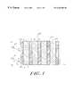
- FIG. 1is a simplified block diagram of an exemplary embodiment of a multilayer periodic dielectric film structure in accordance with the invention
- FIG. 2Ais a graph of the projected band structure of a multilayer film with a light line and Brewster line, exhibiting a reflectivity range of limited angular acceptance;
- FIG. 2Bis a graph of the projected band structure of a multilayer film together with the light line and Brewster line, showing an omnidirectional reflectance range at the first and second harmonic;
- FIG. 3is a graph of the range to midrange ratio for the fundamental frequency range of omnidirectional reflection plotted as contours
- FIG. 4is a series of graphs showing the calculated (solid line) and measured (dashed line) reflectance (%) as a function of wavelength for TM and TE modes at normal, 45°, and 80° angles of incidence, thus showing an omnidirectional reflectivity band;
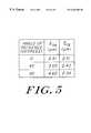
- FIG. 5is a table showing that ⁇ is a monotonically increasing function of the incident angle for the TM mode of an omnidirectional reflector
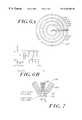
- FIG. 6Ais a simplified block diagram cross section of an exemplary structure
- FIG. 6Bis a corresponding cross section radial index of refraction profile of the structure in FIG. 6A.
- FIG. 7is a cross section of a simplified schematic diagram of a coextrusion assembly in accordance with the invention.
- FIG. 1is a simplified block diagram of an exemplary embodiment of a multilayer periodic dielectric film structure 100 in accordance with the invention.
- h 1 and h 2are the layer thickness
- n 1 and n 2are the indices of refraction of the respective layers 104 and 102 .
- the wave vector together with the normal to the periodic structure 100defines a mirror plane of symmetry that allows distinguishing between two independent electromagnetic modes: transverse electric (TE) modes and transverse magnetic (TM) modes.
- TEtransverse electric
- TMtransverse magnetic
- the distribution of the electric field of the TE mode (or the magnetic field in the TM mode) in a particular layer within the stratified structurecan be written as a sum of two plane waves traveling in opposite directions.
- the amplitudes of the two plane waves in a particular layer ⁇ of one cellare related to the amplitudes in the same layer of an adjacent cell by a unitary 2 ⁇ 2 translation matrix U ( ⁇ ) .
- E K ( x,y )E K ( X ) e ikx e ik y y , (1)
- E K (x)is periodic, with a period of length a, and K is the Bloch wave number given by
- Solutions of the infinite systemcan be propagating or evanescent, corresponding to real or imaginary Bloch wave numbers, respectively.
- the solution of Eq. 2defines the band structure for the infinite system, ⁇ (K,k y ).
- FIGS. 2A and 2Bare examples of such projected structures.
- FIG. 2Bis a graph of the projected band structure of a multilayer film together with the light line 204 and Brewster line 206 , showing an omnidirectional reflectance range at the first and second harmonic.
- the area 208 and 210highlight phase space where K is strictly real, i.e., regions of propagating states.
- the area 212(white) represents regions containing evanescent states.
- the areas 214 and 216represent omnidirectional reflectance ranges.
- the shape of the projected band structures for the multilayer film structurecan be understood intuitively.
- the bandgap for waves travelling normal to the layersis recovered.
- the bandscurve upward in frequency.
- the modesbecome largely confined to the slabs with the high index of refraction and do not couple between layers (and are therefore independent of k x ).
- the translational symmetry in the directions parallel to the layersis preserved, hence k y remains a conserved quantity. In the direction perpendicular to the layers, the translational symmetry no longer exists. Nevertheless, the K-number, as defined in Eq. 2, is still relevant, because it is determined purely by the dielectric and structural property of a single bilayer. In regions where K is imaginary, the electromagnetic field is strongly attenuated. As the number of layers is increased, the transmission coefficient decreases exponentially, while the reflectivity approaches unity.
- the states in FIG. 2A that are lying in the restricted phase space defined by the light line 200 and that have a ( ⁇ ,k y ) corresponding to the propagating solutions (gray areas 208 ) of the structurecan propagate in both the homogeneous medium and in the structure. These waves will partially or entirely transmit through the film. Those with ( ⁇ , k y ) in the evanescent regions (white areas 212 ) can propagate in the homogeneous medium, but will decay in the structure. Waves corresponding to this portion of phase space will be reflected off the structure.
- the multilayer system leading to FIG. 2Arepresents a structure with a limited reflectivity cone since for any frequency one can always find a k y vector for which a wave at that frequency can propagate in the structure, and hence transmit through the film.
- k y valuesranging from 0 (normal incidence) to 0.285 2 ⁇ /a (90° incidence) in the TE mode
- the necessary and sufficient criterion for omnidirectional reflectivity at a given frequencyis that there exist no transmitting states of the structure inside the light cone. This criterion is satisfied by frequency ranges 214 and 216 in FIG. 2 B. In fact, the system leading to FIG. 2B exhibits two omnidirectional reflectivity ranges.
- FIG. 2Ais an example of a structure, which does not have an omnidirectional reflectivity range even though its Brewster crossing is inaccessible to light coming from the homogeneous medium (the Brewster crossing lies outside of the light cone). This is due to the large group velocity of modes in the lower band edge of the TM mode which allow every frequency to couple to a propagating state in the crystal. This should be contrasted with FIG. 2B, which exhibits an omnidirectional reflectivity range (area 214 ). The high indices of refraction actually allow for the opening of an additional omnidirectional reflectivity range (area 216 ) in the higher harmonic as well.
- a dimensionless parameter used to quantify the extent of the omnidirectional reflection rangeis the range to midrange ratio defined as [ ⁇ h ⁇ 1 )/1/2( ⁇ h + ⁇ 1 ).
- FIG. 3is a a plot of this ratio as a function of n 2 /n 1 and n 1 /n 0 where ⁇ h and ⁇ 1 are determined by solutions of Eq. 3 with quarter wave layer thickness, and n 1 >n 2 .
- the contours in this figurerepresent various equi-omnidirectional ranges for different material index parameters and could be useful for design purposes.
- the criterion for the existence of omnidirectional reflectivitycan be restated as the occurrence of a frequency overlap between the gap at normal incidence and the gap of the TM mode at 90°.
- the maximum range widthis attained for thickness values that are not equal to the quarter wave stack though the increase in bandwidth gained by deviating from the quarter wave stack is typically only a few percent.
- the TM modedefines the lower frequency edge of the omnidirectional range.
- An examplecan be seen in FIG. 2B for a particular choice of the indices of refraction. This can be proven by showing that ⁇ ⁇ ⁇ ⁇ k y ⁇ TM ⁇ ⁇ ⁇ ⁇ ⁇ k y ⁇ TE ( 7 )
- Eq. 7lies in the vectorial nature of the electric field. In the upper portion of the first band the electric field concentrates its energy in the high dielectric regions.
- the electric field in the TM modehas a component in the direction of periodicity. This component forces a larger portion of the electric field into the low dielectric regions. The group velocity of the TM mode is therefore enhanced.
- the electric field of the TE modeis always perpendicular to the direction of periodicity and can concentrate its energy primarily in the high dielectric region.
- a polystyrene-tellurium (PS-Te) materials systemwas chosen to demonstrate omnidirectional reflectivity. Tellurium has a high index of refraction and low loss characteristics in the frequency range of interest. In addition, its relatively low latent heat of condensation together with the high glass transition temperature of the PS minimizes diffusion of Te into the polymer layer.
- PSwhich has a series of absorption peaks in the measurement range, demonstrates the competition between reflectivity and absorption that occurs when an absorption peak is located in the evanescent state region.
- the Te(0.8 ⁇ m) and PS (1.65 ⁇ m) filmswere deposited sequentially to create a nine-layer film.
- a 0.8 ⁇ 0.09 ⁇ m thick layer of tellurium (99.99+%, Strem Chemicals)was vacuum evaporated at 10 ⁇ 6 torr and 7A (Ladd Industries 30000) onto a NaCl 25 mm salt substrate (polished NaCl window, Wilmad Glass).
- the layer thickness and deposition ratewere monitored in-situ using a crystal thickness monitor (Sycon STM 100).
- a 10% solution of polystyrene (Goodyear PS standard, 110,000 g/mol) in toluenewas spin cast at 1000 RPM onto the tellurium coated substrate and allowed to dry for a few hours, the polymer layer thickness is 1.65 ⁇ 0.09 ⁇ m .
- the nine layer film sequencewas Te/PS/Te/PS/Te/PS/Te/PS/Te/PS/Te.
- the optical response of this particular multilayer filmwas designed to have a high reflectivity region in the 10 to 15 ⁇ m range for any angle of incidence (in the experiment we measure from 0° to 80°).
- the optical response at oblique angles of incidencewas measured using a Fourier Transform Infrared Spectrometer (Nicolet 860) fitted with a polarizer (ZnS SpectraTech) and an angular reflectivity stage (VeeMax by SpectraTech).
- the reflectivitywas measured using a Nicolet Infrared Microscope. A freshly evaporated aluminum mirror was used as a background for the reflectance measurements.
- FIG. 4is a series of graphs showing the calculated (solid line) and measured (dashed line) reflectance (%) as a function of wavelength for TM and TE modes at normal, 45°, and 80° angles of incidence, thus showing an omnidirectional reflectivity band.
- FIG. 4illustrates the good agreement between the calculated and measured reflectance spectra. The calculations were done using the transfer matrix method described in F. Abeles, Ann. De Physique 5, 706 (1950), incorporated herein by reference, using the film parameters.
- the frequency location of the omnidirectional rangeis determined by the layer thickness and can be tuned to meet specifications.
- the rangeis calculated from Eq. 6 to be 5.6 ⁇ m and the center wavelength is 12.4 ⁇ m corresponding to a 45% range to midrange ratio shown in dashed lines in FIG. 3 for the experimental index of refraction parameters. These values are in agreement with the measured data.
- the calculationsare for lossless media and therefore do not predict the PS absorption band at ⁇ 13 and 14 microns.
- the PS absorption peakis seen to increase at larger angles of incidence for the TM mode, and decrease for the TE mode.
- the physical basis for this phenomenalies in the relation between the penetration depth and the amount of absorption.
- the penetration lengthis ⁇ Im(1/K), with K the Bloch wave number.
- ⁇is a monotonically increasing function of the incident angle for the TM mode of an omnidirectional reflector, and is relatively constant for the TE mode.
- the magnitude of the imaginary part of the Bloch wave number for a mode lying in the gapis related to its distance from the band edges. This distance increases in the TE mode due to the widening of the gap at increasing angles of incidence and decreases in the TM mode due to the shrinking of the gap.
- the PS-Te structuredoes not have a complete photonic bandgap. Its omnidirectional reflectivity is due instead to the restricted phase space available to the propagating states of the system.
- the materials and processeswere chosen for their low cost and applicability to large area coverage.
- the measurementsshow that a polymer, while lossy in the infrared, can still be used for reflection applications without a considerable sacrifice of performance.
- the possibility of achieving omnidirectional reflectivity itselfis not associated with any particular choice of materials and can be applied to many wavelengths of interest.
- the structure of the inventionoffers metallic-like omnidirectional reflectivity for a wide range of frequencies, and at the same time is of low loss. In addition, it allows the flexibility of frequency selection.
- FIG. 6Ais a simplified block diagram cross section of an exemplary structure 600 .
- FIG. 6Bis a corresponding cross section radial index of refraction profile of the structure 600 .
- the structureconsists of concentric cylindrical layers 604 - 616 with alternating indices of refraction n 1 , n 2 centered on a core 602 of low dielectric material n 0 , such as air.
- the radius of the coreis h 0 and the layer thicknesses are h 1 , h 2 .
- Note that an exemplary embodimentwould involve each layer consisting of different material and corresponding different layer thickness.
- the parameters of the multilayer filmare chosen such that light from any incident angle and polarization is completely reflected by the multilayer for the range of signal frequencies.
- the electromagnetic radiationwill be multi-mode or single-mode depending on the size of the region in which it is confined.
- the electromagnetic radiationcan be multi-mode or single mode depending on the size of the inner core region. For large core radii, the light will be multi-mode and for very small radii the light will be single mode.
- the method of confinement in the OmniguideTM waveguide structureis the polarization independent omnidirectional reflectance of EM waves at the walls of the hollow fiber. The advantages of this mode of confinement are numerous.
- the fiberneed amplification to compensate for absorption losses in the material, and to this end, the fiber is periodically doped with erbium.
- the use of erbiumseverely limits the bandwidth of the fiber. Since the structure of the invention is very low loss and does not need amplification, orders of magnitude increase in the usable bandwidth is possible.
- the omnidirectional multilayer structureprovides a strong confinement mechanism and will propagate signals around very sharp bends as demonstrated in other systems with strong confinement mechanisms.
- Such a multilayer coated fiberwill also be important for improving the delivering power of a fiber tip in a near-field scanning optical microscope.
- the tipis used to deliver optical power with a spot size far smaller than the wavelength of light.
- Metal coatingis currently employed in order to confine light to such a small length scale. Metal coatings have material absorption losses, which in this case limits the maximum delivery power.
- the fiber tip with a multilayer coatingovercomes this problem since it is essentially lossless.
- the ultimate goalis to create a hollow structure with walls made of a multilayer coating in accordance with the structure described heretofore.
- the structuremay be of, but is not limited to, a cylindrical geometry.
- One method to produce such a structureis to take a thin wall hollow fiber made of glass or polymer and coat it with alternating layers of dielectrics.
- the layerscould be made of a polymer or glass as the low refractive index component, and Germanium or Tellurium as the high index material.
- the subsequent low index layerwould be deposited by dipping the fiber in a dilute solution of the polymer, or by evaporating a monomer followed by a rapid polymerization.
- FIG. 7is a cross section of a simplified schematic diagram of a coextrusion assembly 700 in accordance with the invention.
- An extruding device 702provides a structure 704 of alternating layers of high and low index polymer surrounding an air core 706 .
Landscapes
- Physics & Mathematics (AREA)
- Chemical & Material Sciences (AREA)
- Crystallography & Structural Chemistry (AREA)
- General Physics & Mathematics (AREA)
- Optics & Photonics (AREA)
- Optical Filters (AREA)
- Optical Elements Other Than Lenses (AREA)
- Optical Integrated Circuits (AREA)
Abstract
Description


Claims (23)
Priority Applications (2)
| Application Number | Priority Date | Filing Date | Title |
|---|---|---|---|
| US09/418,344US6463200B2 (en) | 1998-10-14 | 1999-10-14 | Omnidirectional multilayer device for enhanced optical waveguiding |
| US10/210,493US6603911B2 (en) | 1998-10-14 | 2002-08-01 | Omnidirectional multilayer device for enhanced optical waveguiding |
Applications Claiming Priority (2)
| Application Number | Priority Date | Filing Date | Title |
|---|---|---|---|
| US10415398P | 1998-10-14 | 1998-10-14 | |
| US09/418,344US6463200B2 (en) | 1998-10-14 | 1999-10-14 | Omnidirectional multilayer device for enhanced optical waveguiding |
Related Child Applications (1)
| Application Number | Title | Priority Date | Filing Date |
|---|---|---|---|
| US10/210,493ContinuationUS6603911B2 (en) | 1998-10-14 | 2002-08-01 | Omnidirectional multilayer device for enhanced optical waveguiding |
Publications (2)
| Publication Number | Publication Date |
|---|---|
| US20020025130A1 US20020025130A1 (en) | 2002-02-28 |
| US6463200B2true US6463200B2 (en) | 2002-10-08 |
Family
ID=22298923
Family Applications (2)
| Application Number | Title | Priority Date | Filing Date |
|---|---|---|---|
| US09/418,344Expired - LifetimeUS6463200B2 (en) | 1998-10-14 | 1999-10-14 | Omnidirectional multilayer device for enhanced optical waveguiding |
| US10/210,493Expired - LifetimeUS6603911B2 (en) | 1998-10-14 | 2002-08-01 | Omnidirectional multilayer device for enhanced optical waveguiding |
Family Applications After (1)
| Application Number | Title | Priority Date | Filing Date |
|---|---|---|---|
| US10/210,493Expired - LifetimeUS6603911B2 (en) | 1998-10-14 | 2002-08-01 | Omnidirectional multilayer device for enhanced optical waveguiding |
Country Status (6)
| Country | Link |
|---|---|
| US (2) | US6463200B2 (en) |
| EP (1) | EP1121614B1 (en) |
| JP (1) | JP3643774B2 (en) |
| CA (1) | CA2346733C (en) |
| DE (1) | DE69926774T2 (en) |
| WO (1) | WO2000022466A1 (en) |
Cited By (29)
| Publication number | Priority date | Publication date | Assignee | Title |
|---|---|---|---|---|
| US20030031852A1 (en)* | 2001-07-16 | 2003-02-13 | Yoel Fink | Method of forming reflecting dielectric mirrors |
| US20030044159A1 (en)* | 2001-04-12 | 2003-03-06 | Emilia Anderson | High index-contrast fiber waveguides and applications |
| US6603911B2 (en)* | 1998-10-14 | 2003-08-05 | Massachusetts Institute Of Technology | Omnidirectional multilayer device for enhanced optical waveguiding |
| US6606440B2 (en)* | 2000-05-15 | 2003-08-12 | Sumitomo Electric Industries, Ltd. | Microstructured optical fiber |
| US6625364B2 (en)* | 2001-01-25 | 2003-09-23 | Omniguide Communications | Low-loss photonic crystal waveguide having large core radius |
| US20040061863A1 (en)* | 2002-08-20 | 2004-04-01 | Digonnet Michel J.F. | Fiber optic sensors with reduced noise |
| US20040137168A1 (en)* | 2002-11-22 | 2004-07-15 | Vladimir Fuflyigin | Dielectric waveguide and method of making the same |
| US20040223715A1 (en)* | 2001-07-16 | 2004-11-11 | Gilles Benoit | Fiber waveguides and methods of making the same |
| US20050018987A1 (en)* | 2002-01-19 | 2005-01-27 | Tobias Ruf | Gas-filled optical fiber for wavelength calibration or measurement |
| US20050226579A1 (en)* | 2004-04-08 | 2005-10-13 | Yoel Fink | Photonic crystal waveguides and systems using such waveguides |
| US20050259934A1 (en)* | 2004-04-08 | 2005-11-24 | Burak Temelkuran | Photonic crystal fibers and medical systems including photonic crystal fibers |
| US20050259942A1 (en)* | 2004-04-08 | 2005-11-24 | Burak Temelkuran | Photonic crystal fibers and medical systems including photonic crystal fibers |
| US20050259933A1 (en)* | 2004-04-08 | 2005-11-24 | Burak Temelkuran | Photonic crystal fibers and medical systems including photonic crystal fibers |
| US20050271340A1 (en)* | 2004-04-08 | 2005-12-08 | Ori Weisberg | Photonic crystal waveguides and systems using such waveguides |
| US6985661B1 (en)* | 1999-04-01 | 2006-01-10 | Nkt Research & Innovation A/S | Photonic crystal fibre and a method for its production |
| US20070009217A1 (en)* | 2005-07-08 | 2007-01-11 | Martin Seifert | Optical fiber article and methods of making |
| US20070058916A1 (en)* | 2005-09-13 | 2007-03-15 | Shih-Shou Lo | Hollow optical waveguide by omni-directional reflectors |
| US20070147752A1 (en)* | 2005-06-10 | 2007-06-28 | Omniguide, Inc. | Photonic crystal fibers and systems using photonic crystal fibers |
| US20080030741A1 (en)* | 2006-06-29 | 2008-02-07 | Digonnet Michel J | Optical sensor utilizing hollow-core photonic bandgap fiber with low phase thermal constant |
| US20080180681A1 (en)* | 2002-08-20 | 2008-07-31 | Digonnet Michel J F | Fiber optic sensor using a bragg fiber |
| WO2008157621A3 (en)* | 2007-06-18 | 2009-03-05 | Cube Technologies Inc E | Methods and apparatuses for waveguiding luminescence generated in a scattering medium |
| US20090284983A1 (en)* | 2008-05-16 | 2009-11-19 | Bart Levine | Intrinsically-safe system for mineshaft illumination |
| US8200854B2 (en)* | 2010-08-05 | 2012-06-12 | Verizon Patent And Licensing Inc. | Smart card driven device configuration changes |
| WO2014043697A2 (en) | 2012-09-17 | 2014-03-20 | Omniguide, Inc. | Devices and methods for laser surgery |
| US9063299B2 (en) | 2009-12-15 | 2015-06-23 | Omni Guide, Inc. | Two-part surgical waveguide |
| EP3245971A1 (en) | 2016-05-16 | 2017-11-22 | Omniguide Inc. | Multi-function handpieces for energy-based surgery |
| US10206744B2 (en) | 2013-03-15 | 2019-02-19 | Omniguide, Inc. | Waveguide locks and counterbalances for waveguide conduits |
| US20190227226A1 (en)* | 2018-01-24 | 2019-07-25 | Stc.Unm | Hollow core optical fiber with light guiding within a hollow region based on transverse anderson localization of light |
| US10426546B2 (en) | 2014-09-18 | 2019-10-01 | Omniguide, Inc. | Laparoscopic handpiece for waveguides |
Families Citing this family (61)
| Publication number | Priority date | Publication date | Assignee | Title |
|---|---|---|---|---|
| CA2320257C (en) | 1998-02-19 | 2005-11-01 | Massachusetts Institute Of Technology | High omnidirectional reflector |
| US6909729B2 (en)* | 2000-10-26 | 2005-06-21 | Massachusetts Institute Of Technology | Dielectric waveguide with transverse index variation that support a zero group velocity mode at a non-zero longitudinal wavevector |
| WO2002059663A1 (en) | 2001-01-25 | 2002-08-01 | Omniguide Communications | Photonic crystal optical waveguides having tailored dispersion profiles |
| EP1366378A4 (en) | 2001-01-31 | 2005-11-09 | Omniguide Comm Inc | Electromagnetic mode conversion in photonic crystal multimode waveguides |
| US6624945B2 (en)* | 2001-02-12 | 2003-09-23 | Massachusetts Institute Of Technology | Thin film filters using omnidirectional reflectors |
| EP1436652A2 (en) | 2001-10-19 | 2004-07-14 | NKT Research & Innovation A/S | Integrated photonic crystal structure and method of producing same |
| AUPR858401A0 (en)* | 2001-10-30 | 2001-11-29 | University Of Sydney, The | A methodof designing a waveguide |
| WO2003062871A1 (en)* | 2002-01-22 | 2003-07-31 | Massachusetts Institute Of Technology | Low-loss ir dielectric material system for broadband multiple-range omnidirectional reflectivity |
| US7321712B2 (en) | 2002-12-20 | 2008-01-22 | Crystal Fibre A/S | Optical waveguide |
| US7346249B2 (en) | 2003-03-21 | 2008-03-18 | Crystal Fibre A/S | Photonic bandgap optical waveguide with anti-resonant core boundary |
| US7361171B2 (en) | 2003-05-20 | 2008-04-22 | Raydiance, Inc. | Man-portable optical ablation system |
| GB2403816A (en)* | 2003-07-11 | 2005-01-12 | Fujitsu Ltd | Optical device with radial discontinuities in the refractive index |
| US7023533B2 (en) | 2003-08-01 | 2006-04-04 | Lucent Technologies Inc. | System and method for determining propagation characteristics of photonic structures |
| US7367969B2 (en) | 2003-08-11 | 2008-05-06 | Raydiance, Inc. | Ablative material removal with a preset removal rate or volume or depth |
| US8173929B1 (en) | 2003-08-11 | 2012-05-08 | Raydiance, Inc. | Methods and systems for trimming circuits |
| US9022037B2 (en) | 2003-08-11 | 2015-05-05 | Raydiance, Inc. | Laser ablation method and apparatus having a feedback loop and control unit |
| US20050065502A1 (en)* | 2003-08-11 | 2005-03-24 | Richard Stoltz | Enabling or blocking the emission of an ablation beam based on color of target |
| US8921733B2 (en) | 2003-08-11 | 2014-12-30 | Raydiance, Inc. | Methods and systems for trimming circuits |
| US7115514B2 (en) | 2003-10-02 | 2006-10-03 | Raydiance, Inc. | Semiconductor manufacturing using optical ablation |
| US7143769B2 (en) | 2003-08-11 | 2006-12-05 | Richard Stoltz | Controlling pulse energy of an optical amplifier by controlling pump diode current |
| KR100543708B1 (en)* | 2003-12-17 | 2006-01-20 | 삼성전자주식회사 | Optical mode converter using omni-directional reflector |
| US7413847B2 (en) | 2004-02-09 | 2008-08-19 | Raydiance, Inc. | Semiconductor-type processing for solid-state lasers |
| US7787734B2 (en)* | 2004-12-03 | 2010-08-31 | The Invention Science Fund I, Llc | Photonic crystal energy converter |
| US7499619B2 (en)* | 2004-12-03 | 2009-03-03 | Searete | Photonic crystal energy converter |
| US7333705B2 (en) | 2004-12-03 | 2008-02-19 | Searete Llc | Photonic crystal energy converter |
| US7349452B2 (en) | 2004-12-13 | 2008-03-25 | Raydiance, Inc. | Bragg fibers in systems for the generation of high peak power light |
| CN100360961C (en)* | 2004-12-31 | 2008-01-09 | 燕山大学 | omnidirectional image mirror |
| US8135050B1 (en) | 2005-07-19 | 2012-03-13 | Raydiance, Inc. | Automated polarization correction |
| US7245419B2 (en) | 2005-09-22 | 2007-07-17 | Raydiance, Inc. | Wavelength-stabilized pump diodes for pumping gain media in an ultrashort pulsed laser system |
| US7099533B1 (en) | 2005-11-08 | 2006-08-29 | Chenard Francois | Fiber optic infrared laser beam delivery system |
| US7308171B2 (en) | 2005-11-16 | 2007-12-11 | Raydiance, Inc. | Method and apparatus for optical isolation in high power fiber-optic systems |
| US7436866B2 (en) | 2005-11-30 | 2008-10-14 | Raydiance, Inc. | Combination optical isolator and pulse compressor |
| US7444049B1 (en) | 2006-01-23 | 2008-10-28 | Raydiance, Inc. | Pulse stretcher and compressor including a multi-pass Bragg grating |
| US8189971B1 (en) | 2006-01-23 | 2012-05-29 | Raydiance, Inc. | Dispersion compensation in a chirped pulse amplification system |
| US8232687B2 (en) | 2006-04-26 | 2012-07-31 | Raydiance, Inc. | Intelligent laser interlock system |
| US7529456B2 (en)* | 2006-03-17 | 2009-05-05 | Searete Llc | Photonic crystal surface states |
| US20090196561A1 (en)* | 2006-03-17 | 2009-08-06 | Searete Llc, A Limited Liability Corporation Of The State Of Delaware | Photonic crystal surface states |
| US7529454B2 (en)* | 2006-03-17 | 2009-05-05 | Searete Llc | Photonic crystal surface states |
| US7822347B1 (en) | 2006-03-28 | 2010-10-26 | Raydiance, Inc. | Active tuning of temporal dispersion in an ultrashort pulse laser system |
| US20080177257A1 (en)* | 2007-01-23 | 2008-07-24 | Smith Ronald T | Thermally robust illumination probe tip |
| US10690823B2 (en) | 2007-08-12 | 2020-06-23 | Toyota Motor Corporation | Omnidirectional structural color made from metal and dielectric layers |
| US8323391B2 (en) | 2007-08-12 | 2012-12-04 | Toyota Motor Engineering & Manufacturing North America, Inc. | Omnidirectional structural color paint |
| US9229140B2 (en) | 2007-08-12 | 2016-01-05 | Toyota Motor Engineering & Manufacturing North America, Inc. | Omnidirectional UV-IR reflector |
| US10788608B2 (en) | 2007-08-12 | 2020-09-29 | Toyota Jidosha Kabushiki Kaisha | Non-color shifting multilayer structures |
| US9063291B2 (en) | 2007-08-12 | 2015-06-23 | Toyota Motor Engineering & Manufacturing North America, Inc. | Omnidirectional reflector |
| US9612369B2 (en) | 2007-08-12 | 2017-04-04 | Toyota Motor Engineering & Manufacturing North America, Inc. | Red omnidirectional structural color made from metal and dielectric layers |
| US9739917B2 (en) | 2007-08-12 | 2017-08-22 | Toyota Motor Engineering & Manufacturing North America, Inc. | Red omnidirectional structural color made from metal and dielectric layers |
| US10870740B2 (en) | 2007-08-12 | 2020-12-22 | Toyota Jidosha Kabushiki Kaisha | Non-color shifting multilayer structures and protective coatings thereon |
| US10048415B2 (en) | 2007-08-12 | 2018-08-14 | Toyota Motor Engineering & Manufacturing North America, Inc. | Non-dichroic omnidirectional structural color |
| CN101803275B (en)* | 2007-10-31 | 2012-07-25 | 朗讯科技公司 | Method for generating a real time billing information in a packet switching based network and network element |
| US8125704B2 (en) | 2008-08-18 | 2012-02-28 | Raydiance, Inc. | Systems and methods for controlling a pulsed laser by combining laser signals |
| US8554037B2 (en) | 2010-09-30 | 2013-10-08 | Raydiance, Inc. | Hybrid waveguide device in powerful laser systems |
| CN102522299A (en)* | 2011-12-28 | 2012-06-27 | 东南大学 | Electromagnetic band gap structure, electromagnetic band gap high-impedance substrate and planar travelling wave tube |
| US9658375B2 (en) | 2012-08-10 | 2017-05-23 | Toyota Motor Engineering & Manufacturing North America, Inc. | Omnidirectional high chroma red structural color with combination metal absorber and dielectric absorber layers |
| US9678260B2 (en) | 2012-08-10 | 2017-06-13 | Toyota Motor Engineering & Manufacturing North America, Inc. | Omnidirectional high chroma red structural color with semiconductor absorber layer |
| US9664832B2 (en) | 2012-08-10 | 2017-05-30 | Toyota Motor Engineering & Manufacturing North America, Inc. | Omnidirectional high chroma red structural color with combination semiconductor absorber and dielectric absorber layers |
| WO2015153043A1 (en) | 2014-04-01 | 2015-10-08 | Toyota Motor Engineering & Manufacturing North America, Inc. | Non-color shifting multilayer structures |
| US9212912B1 (en) | 2014-10-24 | 2015-12-15 | Honeywell International Inc. | Ring laser gyroscope on a chip with doppler-broadened gain medium |
| US9810824B2 (en) | 2015-01-28 | 2017-11-07 | Toyota Motor Engineering & Manufacturing North America, Inc. | Omnidirectional high chroma red structural colors |
| US20160299291A1 (en)* | 2015-04-13 | 2016-10-13 | Ziva Corporation | Plasmonic waveguides and waveguiding methods |
| CN115016052B (en)* | 2022-06-29 | 2023-07-28 | 华中科技大学 | Laser omnidirectional reflecting film and application thereof in wearable laser protection field |
Citations (11)
| Publication number | Priority date | Publication date | Assignee | Title |
|---|---|---|---|---|
| EP0195630A2 (en) | 1985-03-18 | 1986-09-24 | Laakmann Electro-Optics Inc. | Hollow waveguide having plural layer dielectric |
| EP0426203A2 (en) | 1986-01-18 | 1991-05-08 | Sumitomo Electric Industries Limited | High power optical fiber |
| WO1994009393A1 (en) | 1992-10-13 | 1994-04-28 | Coherent, Inc. | Optical coating for reflecting visible and longer wavelength radiation having grazing incidence angle |
| GB2288469A (en) | 1994-04-15 | 1995-10-18 | Hitachi Cable | Optical hollow waveguide, its fabrication and laser transmission apparatus using it |
| WO1997001774A1 (en) | 1995-06-26 | 1997-01-16 | Minnesota Mining And Manufacturing Company | High efficiency optical devices |
| US5661839A (en) | 1996-03-22 | 1997-08-26 | The University Of British Columbia | Light guide employing multilayer optical film |
| US5814367A (en) | 1993-08-13 | 1998-09-29 | General Atomics | Broadband infrared and signature control materials and methods of producing the same |
| WO1999047465A1 (en) | 1998-03-16 | 1999-09-23 | Massachusetts Institute Of Technology | Polymer-inorganic multilayer dielectric film |
| US5995696A (en) | 1997-02-07 | 1999-11-30 | Hitachi Cable, Ltd. | Hollow waveguide and method of making same |
| US6043914A (en) | 1998-06-29 | 2000-03-28 | Mci Communications Corporation | Dense WDM in the 1310 nm band |
| US6101032A (en)* | 1994-04-06 | 2000-08-08 | 3M Innovative Properties Company | Light fixture having a multilayer polymeric film |
Family Cites Families (25)
| Publication number | Priority date | Publication date | Assignee | Title |
|---|---|---|---|---|
| EP0060085B1 (en) | 1981-03-06 | 1986-07-16 | Hitachi, Ltd. | Infrared optical fiber |
| US4852968A (en) | 1986-08-08 | 1989-08-01 | American Telephone And Telegraph Company, At&T Bell Laboratories | Optical fiber comprising a refractive index trench |
| US5261016A (en) | 1991-09-26 | 1993-11-09 | At&T Bell Laboratories | Chromatic dispersion compensated optical fiber communication system |
| US5185827A (en) | 1991-09-26 | 1993-02-09 | At&T Bell Laboratories | Apparatus for compensating chromatic dispersion in optical fibers |
| US5448674A (en) | 1992-11-18 | 1995-09-05 | At&T Corp. | Article comprising a dispersion-compensating optical waveguide |
| EP0678196B1 (en) | 1993-01-08 | 2002-04-10 | Massachusetts Institute Of Technology | Low-loss optical and optoelectronic integrated circuits |
| US5882774A (en) | 1993-12-21 | 1999-03-16 | Minnesota Mining And Manufacturing Company | Optical film |
| AU693329B2 (en) | 1995-04-13 | 1998-06-25 | Corning Incorporated | Dispersion managed optical waveguide |
| US5894537A (en) | 1996-01-11 | 1999-04-13 | Corning Incorporated | Dispersion managed optical waveguide |
| US5641956A (en) | 1996-02-02 | 1997-06-24 | F&S, Inc. | Optical waveguide sensor arrangement having guided modes-non guided modes grating coupler |
| US5999679A (en) | 1997-07-14 | 1999-12-07 | Corning Incorporated | Dispersion compensating single mode waveguide |
| GB9713422D0 (en) | 1997-06-26 | 1997-08-27 | Secr Defence | Single mode optical fibre |
| US6339665B1 (en) | 1998-03-26 | 2002-01-15 | Lasercomm Inc. | Apparatus and method for compensation of chromatic dispersion in optical fibers |
| US6404952B1 (en) | 1998-03-26 | 2002-06-11 | Lasercomm Inc. | Optical communication system with chromatic dispersion compensation |
| JP3456143B2 (en) | 1998-05-01 | 2003-10-14 | 信越半導体株式会社 | Laminated materials and optical functional devices |
| US6404966B1 (en) | 1998-05-07 | 2002-06-11 | Nippon Telegraph And Telephone Corporation | Optical fiber |
| JP3072842B2 (en) | 1998-05-07 | 2000-08-07 | 日本電信電話株式会社 | Single mode optical fiber |
| US6222673B1 (en) | 1998-08-18 | 2001-04-24 | Coherent, Inc. | Group-delay-dispersive multilayer-mirror structures and method for designing same |
| US6175671B1 (en) | 1998-10-01 | 2001-01-16 | Nortel Networks Limited | Photonic crystal waveguide arrays |
| CA2346733C (en)* | 1998-10-14 | 2007-01-02 | Massachusetts Institute Of Technology | Omnidirectional reflective multilayer device for confining electromagnetic radiation |
| US6389197B1 (en) | 1999-02-10 | 2002-05-14 | California Institute Of Technology | Coupling system to a microsphere cavity |
| WO2000051268A1 (en) | 1999-02-23 | 2000-08-31 | Lasercomm, Inc. | High order spatial mode transmission system |
| US6301421B1 (en) | 1999-05-27 | 2001-10-09 | Trw Inc. | Photonic crystal fiber lasers and amplifiers for high power |
| US6434311B1 (en) | 1999-06-10 | 2002-08-13 | Lasercomm Inc. | Reducing mode interference in transmission of a high order mode in optical fibers |
| JP3200629B2 (en) | 1999-08-11 | 2001-08-20 | 独立行政法人通信総合研究所 | Optical modulator using photonic bandgap structure and optical modulation method |
- 1999
- 1999-10-14CACA002346733Apatent/CA2346733C/ennot_activeExpired - Lifetime
- 1999-10-14EPEP99951966Apatent/EP1121614B1/ennot_activeExpired - Lifetime
- 1999-10-14USUS09/418,344patent/US6463200B2/ennot_activeExpired - Lifetime
- 1999-10-14WOPCT/US1999/023833patent/WO2000022466A1/enactiveIP Right Grant
- 1999-10-14JPJP2000576308Apatent/JP3643774B2/ennot_activeExpired - Fee Related
- 1999-10-14DEDE69926774Tpatent/DE69926774T2/ennot_activeExpired - Lifetime
- 2002
- 2002-08-01USUS10/210,493patent/US6603911B2/ennot_activeExpired - Lifetime
Patent Citations (12)
| Publication number | Priority date | Publication date | Assignee | Title |
|---|---|---|---|---|
| EP0195630A2 (en) | 1985-03-18 | 1986-09-24 | Laakmann Electro-Optics Inc. | Hollow waveguide having plural layer dielectric |
| EP0426203A2 (en) | 1986-01-18 | 1991-05-08 | Sumitomo Electric Industries Limited | High power optical fiber |
| WO1994009393A1 (en) | 1992-10-13 | 1994-04-28 | Coherent, Inc. | Optical coating for reflecting visible and longer wavelength radiation having grazing incidence angle |
| US5814367A (en) | 1993-08-13 | 1998-09-29 | General Atomics | Broadband infrared and signature control materials and methods of producing the same |
| US6101032A (en)* | 1994-04-06 | 2000-08-08 | 3M Innovative Properties Company | Light fixture having a multilayer polymeric film |
| GB2288469A (en) | 1994-04-15 | 1995-10-18 | Hitachi Cable | Optical hollow waveguide, its fabrication and laser transmission apparatus using it |
| WO1997001774A1 (en) | 1995-06-26 | 1997-01-16 | Minnesota Mining And Manufacturing Company | High efficiency optical devices |
| US6080467A (en)* | 1995-06-26 | 2000-06-27 | 3M Innovative Properties Company | High efficiency optical devices |
| US5661839A (en) | 1996-03-22 | 1997-08-26 | The University Of British Columbia | Light guide employing multilayer optical film |
| US5995696A (en) | 1997-02-07 | 1999-11-30 | Hitachi Cable, Ltd. | Hollow waveguide and method of making same |
| WO1999047465A1 (en) | 1998-03-16 | 1999-09-23 | Massachusetts Institute Of Technology | Polymer-inorganic multilayer dielectric film |
| US6043914A (en) | 1998-06-29 | 2000-03-28 | Mci Communications Corporation | Dense WDM in the 1310 nm band |
Non-Patent Citations (11)
| Title |
|---|
| "Current Status of Flexible Waveguides for IR Laser Radiation Transmission" by Gannot et al., IEEE Journal of Selected Topics In Quantum Electronics, vol.2, No. 4, Dec. 1996, pp. 880-888. |
| Brechet et al., "Analysis of Bandpass Filtering Behaviour of Singlemode Depressed-core-index Photonic-bandgap Fibre," Electronics Letters, vol. 36, No. 10, pp. 870-871, May 11, 2000. |
| Brechet et al., "Singlemode Propagation into Depressed-core-index Photonic-bandgap Fibre Designed for Zero-dispersion Propagation at Short Wavelengths," Electronics Letters, vol. 36, No. 6, pp. 514-515, Mar. 16, 2000. |
| Doran et al., "Cylindrical Bragg Fibers: A Design and Feasibility Study for Optical Communications," Journal of Lightwave Technology, vol. LT-1, No. 4, pp. 588-590, Dec. 1983,. |
| Fink et al., "A Dielectric Omnidirectional Reflector," Science, vol. 282, pp. 1679-1682, Nov. 27, 1998. |
| Lazarchik, "Bragg Fiber Lightguides," originally published in Radiotekhnika I Elektronika, No. 1, 1988, pp. 36-43. |
| Marcatili et al., "Hollow Metallic and Dielectric Waveguides for Long Distance Optical Transmission and Lasers," The Bell System Technical Journal, pp. 1783-1809, Jul. 1964. |
| Martijn et al., "Differential Losses in Bragg Fibers," J.Appl.Phys., 76(2), pp. 680-688, Jul. 15, 1994. |
| Miyagi et al., "Design Theory of Dielectric-Coated Circular Metallic Waveguides for Infrared Transmission," Journal of Lightwave Technology, vol. LT-2, No. 2, pp. 116-126, Apr. 1984. |
| Miyagi et al., "Transmission Characteristics of Dielectric-Coated Metallic Waveguide for Infrared Transmission: Slab Waveguide Model," IEEE Journal of Quantum Electronics, vol. QE-19, No. 2, pp. 136-145, Feb. 1983. |
| Yeh et al., "Theory of Bragg Fiber," Journal of the Optical Society of America, vol. 68, No. 9, pp. 1196-1201, Sep. 1978. |
Cited By (66)
| Publication number | Priority date | Publication date | Assignee | Title |
|---|---|---|---|---|
| US6603911B2 (en)* | 1998-10-14 | 2003-08-05 | Massachusetts Institute Of Technology | Omnidirectional multilayer device for enhanced optical waveguiding |
| US6985661B1 (en)* | 1999-04-01 | 2006-01-10 | Nkt Research & Innovation A/S | Photonic crystal fibre and a method for its production |
| US6606440B2 (en)* | 2000-05-15 | 2003-08-12 | Sumitomo Electric Industries, Ltd. | Microstructured optical fiber |
| US7072553B2 (en)* | 2001-01-25 | 2006-07-04 | Omniguide Communications | Low-loss photonic crystal waveguide having large core radius |
| US6625364B2 (en)* | 2001-01-25 | 2003-09-23 | Omniguide Communications | Low-loss photonic crystal waveguide having large core radius |
| US20040013379A1 (en)* | 2001-01-25 | 2004-01-22 | Omniguide Communications, A Delaware Corporation | Low-loss photonic crystal waveguide having large core radius |
| US7142756B2 (en) | 2001-04-12 | 2006-11-28 | Omniguide, Inc. | High index-contrast fiber waveguides and applications |
| US20030044159A1 (en)* | 2001-04-12 | 2003-03-06 | Emilia Anderson | High index-contrast fiber waveguides and applications |
| US7190875B2 (en) | 2001-04-12 | 2007-03-13 | Omniguide, Inc. | Fiber waveguide formed from chalcogenide glass and polymer |
| US20050259944A1 (en)* | 2001-04-12 | 2005-11-24 | Emilia Anderson | High index-contrast fiber waveguides and applications |
| US20030031852A1 (en)* | 2001-07-16 | 2003-02-13 | Yoel Fink | Method of forming reflecting dielectric mirrors |
| US20040223715A1 (en)* | 2001-07-16 | 2004-11-11 | Gilles Benoit | Fiber waveguides and methods of making the same |
| US8516856B2 (en) | 2001-07-16 | 2013-08-27 | Massachusetts Institute Of Technology | Methods of making fiber waveguides from multilayer structures |
| US7311962B2 (en) | 2001-07-16 | 2007-12-25 | Massachusetts Institute Of Technology | Method of forming reflecting dielectric mirrors |
| US7272285B2 (en) | 2001-07-16 | 2007-09-18 | Massachusetts Institute Of Technology | Fiber waveguides and methods of making the same |
| US20060201206A1 (en)* | 2001-07-16 | 2006-09-14 | Gilles Benoit | Fiber waveguides and methods of making the same |
| US20050018987A1 (en)* | 2002-01-19 | 2005-01-27 | Tobias Ruf | Gas-filled optical fiber for wavelength calibration or measurement |
| US20060257068A1 (en)* | 2002-01-19 | 2006-11-16 | Agilent Technologies, Inc. | Gas-filled optical fiber for wavelength calibration or measurement |
| US20040061863A1 (en)* | 2002-08-20 | 2004-04-01 | Digonnet Michel J.F. | Fiber optic sensors with reduced noise |
| US8068231B2 (en)* | 2002-08-20 | 2011-11-29 | The Board Of Trustees Of The Leland Stanford Junior University | Fiber optic sensor using a Bragg fiber |
| US20100220332A1 (en)* | 2002-08-20 | 2010-09-02 | Digonnet Michel J F | Fiber optic sensor using a bragg fiber |
| US7738109B2 (en) | 2002-08-20 | 2010-06-15 | The Board Of Trustees Of The Leland Stanford Junior University | Fiber optic sensor using a Bragg fiber |
| US20080180681A1 (en)* | 2002-08-20 | 2008-07-31 | Digonnet Michel J F | Fiber optic sensor using a bragg fiber |
| US8233151B2 (en) | 2002-08-20 | 2012-07-31 | The Board Of Trustees Of The Leland Stanford Junior University | Fiber optic sensor using a hollow core fiber |
| US8427651B2 (en) | 2002-08-20 | 2013-04-23 | The Board Of Trustees Of The Leland Stanford Junior University | Optical sensor using a hollow core waveguide |
| US20040137168A1 (en)* | 2002-11-22 | 2004-07-15 | Vladimir Fuflyigin | Dielectric waveguide and method of making the same |
| US7854149B2 (en) | 2002-11-22 | 2010-12-21 | Omniguide, Inc. | Dielectric waveguide and method of making the same |
| US20080141724A1 (en)* | 2002-11-22 | 2008-06-19 | Omniguide, Inc. | Dielectric waveguide and method of making the same |
| US20040141702A1 (en)* | 2002-11-22 | 2004-07-22 | Vladimir Fuflyigin | Dielectric waveguide and method of making the same |
| US7310466B2 (en) | 2004-04-08 | 2007-12-18 | Omniguide, Inc. | Photonic crystal waveguides and systems using such waveguides |
| US8761561B2 (en) | 2004-04-08 | 2014-06-24 | Omniguide, Inc. | Medical system including a flexible waveguide mechanically coupled to an actuator |
| US20050259942A1 (en)* | 2004-04-08 | 2005-11-24 | Burak Temelkuran | Photonic crystal fibers and medical systems including photonic crystal fibers |
| US7231122B2 (en) | 2004-04-08 | 2007-06-12 | Omniguide, Inc. | Photonic crystal waveguides and systems using such waveguides |
| US20050259934A1 (en)* | 2004-04-08 | 2005-11-24 | Burak Temelkuran | Photonic crystal fibers and medical systems including photonic crystal fibers |
| US7331954B2 (en) | 2004-04-08 | 2008-02-19 | Omniguide, Inc. | Photonic crystal fibers and medical systems including photonic crystal fibers |
| US7349589B2 (en) | 2004-04-08 | 2008-03-25 | Omniguide, Inc. | Photonic crystal fibers and medical systems including photonic crystal fibers |
| US20050259933A1 (en)* | 2004-04-08 | 2005-11-24 | Burak Temelkuran | Photonic crystal fibers and medical systems including photonic crystal fibers |
| US7991258B2 (en) | 2004-04-08 | 2011-08-02 | Omniguide, Inc. | Photonic crystal fibers and medical systems including photonic crystal fibers |
| US20050271340A1 (en)* | 2004-04-08 | 2005-12-08 | Ori Weisberg | Photonic crystal waveguides and systems using such waveguides |
| US7167622B2 (en) | 2004-04-08 | 2007-01-23 | Omniguide, Inc. | Photonic crystal fibers and medical systems including photonic crystal fibers |
| US8320725B2 (en) | 2004-04-08 | 2012-11-27 | Omniguide, Inc. | Photonic crystal fibers and medical systems including photonic crystal fibers |
| US20050226579A1 (en)* | 2004-04-08 | 2005-10-13 | Yoel Fink | Photonic crystal waveguides and systems using such waveguides |
| US20070053640A1 (en)* | 2005-03-04 | 2007-03-08 | James Goell | Photonic crystal fibers having a preferred bending plane and systems that use such fibers |
| US8280212B2 (en) | 2005-03-04 | 2012-10-02 | Omniguide, Inc. | Photonic crystal fibers having a preferred bending plane and systems that use such fibers |
| US20070147752A1 (en)* | 2005-06-10 | 2007-06-28 | Omniguide, Inc. | Photonic crystal fibers and systems using photonic crystal fibers |
| US20070009217A1 (en)* | 2005-07-08 | 2007-01-11 | Martin Seifert | Optical fiber article and methods of making |
| US7450808B2 (en) | 2005-07-08 | 2008-11-11 | Nuffern | Optical fiber article and methods of making |
| US7239786B2 (en) | 2005-09-13 | 2007-07-03 | National Central University | Hollow optical waveguide by omni-directional reflectors |
| US20070058916A1 (en)* | 2005-09-13 | 2007-03-15 | Shih-Shou Lo | Hollow optical waveguide by omni-directional reflectors |
| US7619743B2 (en) | 2006-06-29 | 2009-11-17 | The Board Of Trustees Of The Leland Stanford Junior University | Optical sensor utilizing hollow-core photonic bandgap fiber with low phase thermal constant |
| US20100039649A1 (en)* | 2006-06-29 | 2010-02-18 | The Board Of Trustees Of The Leland Stanford Junior University | Optical sensor utilizing hollow-core photonic bandgap fiber with low phase thermal constant |
| US7911620B2 (en) | 2006-06-29 | 2011-03-22 | The Board Of Trustees Of The Leland Stanford Junior University | Optical sensor utilizing hollow-core photonic bandgap fiber with low phase thermal constant |
| US20080030741A1 (en)* | 2006-06-29 | 2008-02-07 | Digonnet Michel J | Optical sensor utilizing hollow-core photonic bandgap fiber with low phase thermal constant |
| WO2008157621A3 (en)* | 2007-06-18 | 2009-03-05 | Cube Technologies Inc E | Methods and apparatuses for waveguiding luminescence generated in a scattering medium |
| US20090110356A1 (en)* | 2007-06-18 | 2009-04-30 | Xiao-Dong Xiang | Methods and apparatuses for waveguiding luminescence generated in a scattering medium |
| US20090284983A1 (en)* | 2008-05-16 | 2009-11-19 | Bart Levine | Intrinsically-safe system for mineshaft illumination |
| US9063299B2 (en) | 2009-12-15 | 2015-06-23 | Omni Guide, Inc. | Two-part surgical waveguide |
| US8200854B2 (en)* | 2010-08-05 | 2012-06-12 | Verizon Patent And Licensing Inc. | Smart card driven device configuration changes |
| US8533369B2 (en) | 2010-08-05 | 2013-09-10 | Cellco Partnership | Smart card driven device configuration changes |
| WO2014043697A2 (en) | 2012-09-17 | 2014-03-20 | Omniguide, Inc. | Devices and methods for laser surgery |
| US10492876B2 (en) | 2012-09-17 | 2019-12-03 | Omniguide, Inc. | Devices and methods for laser surgery |
| US10206744B2 (en) | 2013-03-15 | 2019-02-19 | Omniguide, Inc. | Waveguide locks and counterbalances for waveguide conduits |
| US10426546B2 (en) | 2014-09-18 | 2019-10-01 | Omniguide, Inc. | Laparoscopic handpiece for waveguides |
| EP3245971A1 (en) | 2016-05-16 | 2017-11-22 | Omniguide Inc. | Multi-function handpieces for energy-based surgery |
| US20190227226A1 (en)* | 2018-01-24 | 2019-07-25 | Stc.Unm | Hollow core optical fiber with light guiding within a hollow region based on transverse anderson localization of light |
| US10578797B2 (en)* | 2018-01-24 | 2020-03-03 | Stc.Unm | Hollow core optical fiber with light guiding within a hollow region based on transverse anderson localization of light |
Also Published As
| Publication number | Publication date |
|---|---|
| US20020025130A1 (en) | 2002-02-28 |
| EP1121614B1 (en) | 2005-08-17 |
| US6603911B2 (en) | 2003-08-05 |
| JP2002527788A (en) | 2002-08-27 |
| CA2346733C (en) | 2007-01-02 |
| JP3643774B2 (en) | 2005-04-27 |
| EP1121614A1 (en) | 2001-08-08 |
| WO2000022466A1 (en) | 2000-04-20 |
| DE69926774T2 (en) | 2006-06-01 |
| CA2346733A1 (en) | 2000-04-20 |
| DE69926774D1 (en) | 2005-09-22 |
| US20020191929A1 (en) | 2002-12-19 |
Similar Documents
| Publication | Publication Date | Title |
|---|---|---|
| US6463200B2 (en) | Omnidirectional multilayer device for enhanced optical waveguiding | |
| Fink et al. | Guiding optical light in air using an all-dielectric structure | |
| EP1305659B1 (en) | Surface plasmon polariton band gap structures | |
| US7321713B2 (en) | Silicon based on-chip photonic band gap cladding waveguide | |
| Robertson | Experimental measurement of the effect of termination on surface electromagnetic waves in one-dimensional photonic bandgap arrays | |
| US7311962B2 (en) | Method of forming reflecting dielectric mirrors | |
| US20090097809A1 (en) | Ferroelectric all-polymer hollow bragg fibers for terahertz guidance | |
| JP2002504711A (en) | Photonic crystal omnidirectional reflector | |
| Harrington et al. | Review of hollow waveguide technology | |
| González-Valencia et al. | Side-polished photonic crystal fiber sensor with ultra-high figure of merit based on Bloch-like surface wave resonance | |
| Wu et al. | Complete redshift photonic bandgap and dual-wavelength polarization selection in periodic multilayer structure containing hyperbolic metamaterial | |
| Mei et al. | Transformation one-dimensional photonic crystal omnidirectional reflector | |
| Cheng et al. | Negative Goos-Hänchen shift in reflection from subwavelength gratings | |
| Chuliá-Jordán et al. | Comparison of the different bandgap cavities in a metallic four-mode plasmonic structure | |
| Yu et al. | Construction of a dual-core hollow waveguide for visible and mid-infrared light transmission based on PTFE tubing and UV gel | |
| Barton et al. | Preparation of Bragg mirrors on silica optical fibers and inner walls of silica capillaries by employing the sol–gel method, and titanium and silicon alkoxides | |
| Wei et al. | Design and optimization of two-dimensional porous lithium niobate grating birefringent Bloch surface wave sensor with high sensitivity and quality factor | |
| Charbonneau et al. | Long-range plasmon-polariton wave propagation in thin metal films of finite-width excited using an end-fire technique | |
| Dai et al. | Polarization beam splitter constructed by symmetrical metal-cladding waveguide | |
| Sahkova et al. | Comparison of Binary and Ternary Layered Structures as Claddings of Bragg Waveguide | |
| Vorgul et al. | Design and optimisation of multimode 1D photonic band gap waveguide | |
| Tenev et al. | High plasmonic resonant reflection and transmission at continuous metal films on undulated photosensitive polymer | |
| Harrington | Infrared hollow waveguides: An update | |
| Carniglia et al. | Direct observation of waveguided scattered light in multilayer dielectric thin films | |
| Wächter et al. | Leaky waveguides for low k-measurement: From structure design to loss evaluation |
Legal Events
| Date | Code | Title | Description |
|---|---|---|---|
| AS | Assignment | Owner name:UNITED STATES AIR FORCE, VIRGINIA Free format text:CONFIRMATORY LICENSE;ASSIGNOR:M.I.T.;REEL/FRAME:010456/0986 Effective date:19991210 | |
| AS | Assignment | Owner name:MASSACHUSETTS INSTITUTE OF TECHNOLOGY, MASSACHUSET Free format text:ASSIGNMENT OF ASSIGNORS INTEREST;ASSIGNORS:FINK, YOEL;FAN, SHANHUI;THOMAS, EDWIN;AND OTHERS;REEL/FRAME:010612/0140 Effective date:20000202 | |
| AS | Assignment | Owner name:NATIONAL SCIENCE FOUNDATION, VIRGINIA Free format text:CONFIRMATORY LICENSE;ASSIGNOR:MASSACHUSETTS INSTITUTE OF TECHNOLOGY;REEL/FRAME:013078/0779 Effective date:20020326 | |
| STCF | Information on status: patent grant | Free format text:PATENTED CASE | |
| CC | Certificate of correction | ||
| FEPP | Fee payment procedure | Free format text:PAT HOLDER NO LONGER CLAIMS SMALL ENTITY STATUS, ENTITY STATUS SET TO UNDISCOUNTED (ORIGINAL EVENT CODE: STOL); ENTITY STATUS OF PATENT OWNER: LARGE ENTITY | |
| REFU | Refund | Free format text:REFUND - PAYMENT OF MAINTENANCE FEE, 4TH YEAR, LARGE ENTITY (ORIGINAL EVENT CODE: R1551); ENTITY STATUS OF PATENT OWNER: LARGE ENTITY Free format text:REFUND - SURCHARGE, PETITION TO ACCEPT PYMT AFTER EXP, UNINTENTIONAL (ORIGINAL EVENT CODE: R2551); ENTITY STATUS OF PATENT OWNER: LARGE ENTITY | |
| FPAY | Fee payment | Year of fee payment:4 | |
| FEPP | Fee payment procedure | Free format text:PAYOR NUMBER ASSIGNED (ORIGINAL EVENT CODE: ASPN); ENTITY STATUS OF PATENT OWNER: LARGE ENTITY | |
| FPAY | Fee payment | Year of fee payment:8 | |
| FPAY | Fee payment | Year of fee payment:12 |