US6462800B1 - Electrode contact structure for a liquid crystal display device and manufacturing method thereof - Google Patents
Electrode contact structure for a liquid crystal display device and manufacturing method thereofDownload PDFInfo
- Publication number
- US6462800B1 US6462800B1US09/607,576US60757600AUS6462800B1US 6462800 B1US6462800 B1US 6462800B1US 60757600 AUS60757600 AUS 60757600AUS 6462800 B1US6462800 B1US 6462800B1
- Authority
- US
- United States
- Prior art keywords
- bus line
- electrode
- pixel electrode
- pixel
- contact hole
- Prior art date
- Legal status (The legal status is an assumption and is not a legal conclusion. Google has not performed a legal analysis and makes no representation as to the accuracy of the status listed.)
- Expired - Lifetime, expires
Links
Images


Classifications
- G—PHYSICS
- G02—OPTICS
- G02F—OPTICAL DEVICES OR ARRANGEMENTS FOR THE CONTROL OF LIGHT BY MODIFICATION OF THE OPTICAL PROPERTIES OF THE MEDIA OF THE ELEMENTS INVOLVED THEREIN; NON-LINEAR OPTICS; FREQUENCY-CHANGING OF LIGHT; OPTICAL LOGIC ELEMENTS; OPTICAL ANALOGUE/DIGITAL CONVERTERS
- G02F1/00—Devices or arrangements for the control of the intensity, colour, phase, polarisation or direction of light arriving from an independent light source, e.g. switching, gating or modulating; Non-linear optics
- G02F1/01—Devices or arrangements for the control of the intensity, colour, phase, polarisation or direction of light arriving from an independent light source, e.g. switching, gating or modulating; Non-linear optics for the control of the intensity, phase, polarisation or colour
- G02F1/13—Devices or arrangements for the control of the intensity, colour, phase, polarisation or direction of light arriving from an independent light source, e.g. switching, gating or modulating; Non-linear optics for the control of the intensity, phase, polarisation or colour based on liquid crystals, e.g. single liquid crystal display cells
- G02F1/133—Constructional arrangements; Operation of liquid crystal cells; Circuit arrangements
- G02F1/1333—Constructional arrangements; Manufacturing methods
- G02F1/1343—Electrodes
- G02F1/134309—Electrodes characterised by their geometrical arrangement
- G02F1/134363—Electrodes characterised by their geometrical arrangement for applying an electric field parallel to the substrate, i.e. in-plane switching [IPS]
- G—PHYSICS
- G02—OPTICS
- G02F—OPTICAL DEVICES OR ARRANGEMENTS FOR THE CONTROL OF LIGHT BY MODIFICATION OF THE OPTICAL PROPERTIES OF THE MEDIA OF THE ELEMENTS INVOLVED THEREIN; NON-LINEAR OPTICS; FREQUENCY-CHANGING OF LIGHT; OPTICAL LOGIC ELEMENTS; OPTICAL ANALOGUE/DIGITAL CONVERTERS
- G02F1/00—Devices or arrangements for the control of the intensity, colour, phase, polarisation or direction of light arriving from an independent light source, e.g. switching, gating or modulating; Non-linear optics
- G02F1/01—Devices or arrangements for the control of the intensity, colour, phase, polarisation or direction of light arriving from an independent light source, e.g. switching, gating or modulating; Non-linear optics for the control of the intensity, phase, polarisation or colour
- G02F1/13—Devices or arrangements for the control of the intensity, colour, phase, polarisation or direction of light arriving from an independent light source, e.g. switching, gating or modulating; Non-linear optics for the control of the intensity, phase, polarisation or colour based on liquid crystals, e.g. single liquid crystal display cells
- G02F1/133—Constructional arrangements; Operation of liquid crystal cells; Circuit arrangements
- G02F1/136—Liquid crystal cells structurally associated with a semi-conducting layer or substrate, e.g. cells forming part of an integrated circuit
- G02F1/1362—Active matrix addressed cells
- G02F1/136227—Through-hole connection of the pixel electrode to the active element through an insulation layer
Definitions
- the present inventionrelates to a liquid crystal display device and a method for manufacturing the same, and more particularly to a liquid crystal display device and its manufacturing method capable of reducing line degradation due to a short circuit between a gate bus line and a counter electrode, thereby enhancing a process yield.
- a liquid crystal display deviceis composed of a lower substrate provided with a TFT and a pixel electrode, an upper substrate opposed to the lower substrate and having a color filter, and a liquid crystal layer interposed between the lower and the upper substrate.
- spacersare distributed in the liquid crystal layer for maintaining a fixed distance between the lower and the upper substrate.
- FIG. 1shows the lower substrate having a conventional FFS (Fringe Field Switching) mode structure in a plan view.
- FFSFlexible Field Switching
- a gate bus line 2 and a data bus line 4are arranged on the lower substrate 1 while crossing over each other so as to define an unit pixel, and a thin film transistor (TFT) is disposed adjacent to an intersection point of the gate bus line 2 and the data bus line 4 .
- TFTthin film transistor
- a counter electrode 5is a transparent conductor formed in each unit pixel.
- This counter electrode 5includes a plurality of branches 5 a disposed in an equal spacing, and a body portion 5 b connected to one end of each branch 5 a and joining its own counter electrode 5 to the counter electrode 5 of the adjacent pixel. In this case, a common signal is applied to the counter electrodes 5 .
- a pixel electrode 7is formed in each unit pixel region in such a manner that it overlaps the counter electrode 5 .
- the pixel electrode 7includes a plurality of comb portions 7 a , each extending parallel to the data bus line 4 and inserted between the branches 5 a , and a bar 7 b connected to one end of each comb portion 7 a and contacting with a drain electrode of the thin film transistor (TFT).
- TFTthin film transistor
- the pixel electrode 7is also made of a transparent conductor. Further, the counter electrode 7 and the pixel electrode 7 are insulated from each other by interposing a gate insulating film therebetween.
- an upper substrate(not shown) is opposed to the lower substrate 1 at a distance larger than that between the comb portion 7 a of the pixel electrode 7 and the branch 5 a of the counter electrode 5 , which is not shown in FIG. 1 .
- a liquid crystal layer having a plurality of liquid crystal moleculesis disposed between the lower substrate 1 and the upper substrate.
- the liquid crystal display device of the above-mentioned structure having a high aperture ratio and a high transmittanceis operated as follows.
- a fringe field E including a vertical componentis formed between both electrodes 5 , 7 because the distance between both electrodes 5 , 7 is larger than the distance between the lower and the upper electrode.
- This fringe field Ehas an effect on the whole upper area of the counter electrode 5 and the pixel electrode 7 , so that all of the liquid crystal molecules in the upper area of the electrodes 5 , 7 are operated. Therefore, the high aperture ratio and the high transmittance can be realized.
- the counter electrode 5is formed by ITO (indium tin oxide) and then the gate bus line 2 and the common bus line 6 are formed by a gate metal of an aluminum (Al) series suitable for a larger area in order to prevent corrosion caused by etching of the ITO during a manufacturing process of the lower substrate.
- ITOindium tin oxide
- Alaluminum
- the so constructed conventional liquid crystal display devicehas a drawback that since all of the counter electrodes 5 are connected to the common bus line 6 and constructed in the same layer as the gate bus line 2 , a short circuit is apt to occur between the gate bus line 2 and the counter electrode 5 when a particle 10 happens to be generated as shown in FIG. 1 B. Thus, even if any one portion is short circuited due to the particle 10 , a ‘high’ voltage is always applied to the gate bus line 2 to cause a defect of the gate bus line 2 . This leads to a problem that a process yield for the FFS mode structure is lower by 20% than that for a Twisted Nematic (TN) mode structure.
- TNTwisted Nematic
- the present inventionhas been made to solve the above-mentioned problems occurring in the prior art, and it is an object of the present invention to provide a liquid crystal display device and its manufacturing method, which limit degradation to only one pixel while maintaining a existing process layer structure as it is even if a short circuit occurs between the gate bus line and the pixel electrode in the same layer due to the particle, thereby increasing the process yield.
- liquid crystal display devicein accordance with one aspect of the present invention, the liquid crystal display device comprising a plurality of unit pixels, each unit pixel comprising:
- a pixel electrodeformed in the shape of a plate on a lower substrate by patterning of a first transparent electrode and protruding at its lower end so as to be contacted with one terminal of a thin film transistor;
- a counter electrodeformed over the pixel electrode by using a slit-shaped second transparent electrode and provided with a first contact hole so as to be connected to the lower common bus line;
- a data bus lineintersecting with the gate bus line between two pixel electrodes in the adjacent unit pixel and provided with a second contact hole so as to be connected to the lower pixel electrode.
- a size of the first contact holeis preferably 10 ⁇ 30 ⁇ m.
- a size of the second contact holeis 6 ⁇ 20 ⁇ m.
- a thickness of the pixel electrodeis preferably 400 ⁇ .
- a distance between the common bus line and the pixel electrodeis 5 ⁇ m.
- the data bus lineis composed of a laminate of molybdenum (Mo)/aluminum (Al)/molybdenum (Mo).
- a pixel electrodeon a lower substrate by patterning a first transparent electrode, the pixel having the shape of a plate and protruding at its lower end so as to be contacted with one terminal of a thin film transistor;
- a data bus linein such a manner that it intersects with the gate bus line, forming a source/drain electrode and then providing the source/drain electrode with a second contact hole for connecting the source/drain electrode to the lower pixel electrode;
- FIG. 1is a plan view of a lower substrate of a conventional liquid crystal display device having a FFS mode structure
- FIGS. 2A and 2Bare plan views of a lower substrate of a liquid crystal display device according to a preferred embodiment of the present invention.
- FIG. 2Cis a sectional view taken along line A-A′ in FIG. 2A.
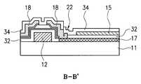
- FIG. 2Dis a sectional view taken along line B-B′ in FIG. 2 A.
- FIGS. 2A and 2Bare plan views of a lower substrate of a liquid crystal display device according to an embodiment of the present invention.
- FIGS. 2C and 2Dare sectional views taken along lines A-A ′ and B-B ′ in FIG. 2A, respectively.
- the liquid crystal display devicecomprises a plurality of unit pixels formed on a lower substrate 11 .
- each unit pixelincludes a pixel electrode 17 , a common bus line 16 , a gate bus line 12 , a counter electrode 15 , a data bus line 14 and thin film transistor.
- the pixel electrode 17is formed on the lower substrate 11 by patterning a first transparent electrode and has the shape of a plate as seen from FIG. 2B showing the state that the data bus line 14 , the counter electrode 15 and the thin film transistor are removed. A lower end of the pixel electrode 17 protrudes in part so as to be in contact with one terminal of the thin film transistor.
- the thin film transistorhas a source/drain electrode 18 .
- the common bus line 16is spaced at a predetermined distance from the pixel electrode 17 . At this time, the distance between the common bus line 16 and the pixel electrode 17 is preferably 5 ⁇ m.
- the gate bus line 12is formed on the opposite side to the common bus line 16 with regard to the pixel electrode 17 .
- the counter electrode 15is formed over tie pixel electrode 17 by using a second transparent electrode and has a plurality of slits tat open to only one side. That is, the counter electrode has a comb-like shape.
- the gate insulation layer 32is formed with a first contact hole 20 for connecting the counter electrode 15 to the common bus line 16 as seen from FIG. 2 C.
- the data bus line 14intersects with the gate bus line 12 between two pixel electrodes 17 in the adjacent unit pixel.
- the gate insulating layer 32is also formed with a second contact hole 22 for connecting the source/drain electrode 18 to the lower pixel electrode 17 as seen from FIG. 2 D.
- sizes of the first and the second contact holeare preferably 10 ⁇ 30 ⁇ m and 6 ⁇ 20 ⁇ m, respectively.
- a thickness of the pixel electrodeis preferably 400 ⁇ .
- the data bus line 14is composed of a laminate of molybdenum (Mo)/aluminum (Al)/molybdenum (Mo).
- the pixel electrode 17is formed by means of patterning of the first transparent electrode (ITO).
- the pixel electrode 17is patterned in the shape of a box and has a thickness of 400 ⁇ .
- the gate bus line 12 and the common bus line 16are formed on the lower substrate 11 by using metal material of an aluminum (Al) series.
- Alaluminum
- the common bus line 16 and the pixel electrode 17 made of the first transparent electrode (ITO)are spaced apart from each other at a predetermined distance (about 5 ⁇ m).
- a gate insulating film 32is vapor-deposited and patterned.
- the patterningis performed on an upper part of the common bus line 16 and predetermined portions of the pixel electrode 17 made of the first transparent electrode (ITO), and then the counter electrode 15 is formed on the patterned part and portions by using the slit-shaped second transparent electrode (ITO).
- the contact hole 22is formed on the pixel electrode 17 in such a manner that the contact hole 22 connects the pixel electrode 17 to the source/drain electrode 18 later on.
- the size of the contact hole 22 on the pixel electrode 17is 10 ⁇ 30 ⁇ m as mentioned above.
- an etch stopper (E/S) and an active layerare formed by patterning.
- the second transparent electrode (ITO)is vapor-deposited and patterned. In this case, patterning is so performed as to form a plurality of slits in the counter electrode 15 .
- the contact hole 20is formed on the common bus line 16 so that the counter electrode 15 is connected to the common bus line 16 in the lower portion.
- the size of contact hole 20 on the common bus line 16is 6 ⁇ 20 ⁇ m as mentioned above.
- the data bus line 14 and the source/drain electrode 18are formed by using non-transparent source/drain metal made of a laminate of molybdenum (Mo)/aluminum (Al)/molybdenum (Mo) and having a thickness of 2000 ⁇ .
- the source/drain electrode 18is connected to the lower pixel electrode 17 made of the box-like first transparent electrode (ITO).
- a protective film 34 made of silicon nitride (SiNx) filmis coated on the resultant product with a thickness of 2000 ⁇ , patterned and opened for the preparation of an outer leader bonding operation (OLB).
- SiNxsilicon nitride
- the existing box-like counter electrodeis connected to the source/drain electrode through the contact hole and so is used as the pixel electrode, and the existing slit-shaped pixel electrode is connected to the non-transparent metallic common bus line through the contact hole and so becomes the counter electrode while maintaining the existing process layer structure as it is, so that even if the short circuit occurs between the gate bus line and the box-like pixel electrode in the same layer due to the particle, degradation as the form of a bright pixel defect is limited to only one pixel. As the result of that, the process yield is enhanced. In a size of 15 inches diagonal, degradation containing up to 5 bright pixels is not fatal in view of image quality, which means that increase of the process yield can be expected.
Landscapes
- Physics & Mathematics (AREA)
- Nonlinear Science (AREA)
- Mathematical Physics (AREA)
- Chemical & Material Sciences (AREA)
- Crystallography & Structural Chemistry (AREA)
- General Physics & Mathematics (AREA)
- Optics & Photonics (AREA)
- Geometry (AREA)
- Liquid Crystal (AREA)
- Devices For Indicating Variable Information By Combining Individual Elements (AREA)
- Thin Film Transistor (AREA)
Abstract
Description
Claims (7)
Applications Claiming Priority (2)
| Application Number | Priority Date | Filing Date | Title |
|---|---|---|---|
| KR10-1999-0025662AKR100494682B1 (en) | 1999-06-30 | 1999-06-30 | Liquid crystal display and manufacturing method thereof |
| KR99-25662 | 1999-06-30 |
Publications (1)
| Publication Number | Publication Date |
|---|---|
| US6462800B1true US6462800B1 (en) | 2002-10-08 |
Family
ID=19597524
Family Applications (1)
| Application Number | Title | Priority Date | Filing Date |
|---|---|---|---|
| US09/607,576Expired - LifetimeUS6462800B1 (en) | 1999-06-30 | 2000-06-29 | Electrode contact structure for a liquid crystal display device and manufacturing method thereof |
Country Status (3)
| Country | Link |
|---|---|
| US (1) | US6462800B1 (en) |
| JP (1) | JP4065651B2 (en) |
| KR (1) | KR100494682B1 (en) |
Cited By (23)
| Publication number | Priority date | Publication date | Assignee | Title |
|---|---|---|---|---|
| US20060139504A1 (en)* | 2004-12-24 | 2006-06-29 | Ahn Byung C | Liquid crystal display device and fabricating method thereof |
| US20060146245A1 (en)* | 2004-12-31 | 2006-07-06 | Ahn Byung C | Liquid crystal display device and fabricating method thereof |
| US20060146213A1 (en)* | 2004-12-31 | 2006-07-06 | Ahn Byung C | Liquid crystal display device and fabricating method thereof |
| US20070263132A1 (en)* | 2006-05-12 | 2007-11-15 | Lg Philips Lcd Co., Ltd. | Liquid crystal display fabrication method |
| US20070291209A1 (en)* | 2006-06-15 | 2007-12-20 | Sakae Tanaka | Low-cost large-screen wide-angle fast-response liquid crystal display apparatus |
| US20080074572A1 (en)* | 2006-09-26 | 2008-03-27 | Samsung Electronics Co., Ltd. | Thin film transistor substrate, method of manufacturing the same, and liquid crystal display panel having the same |
| US20090201449A1 (en)* | 2006-06-26 | 2009-08-13 | Kenji Nishida | Display device |
| CN101022092B (en)* | 2006-02-14 | 2010-12-01 | 株式会社日立显示器 | Manufacturing method of display device |
| US20110032435A1 (en)* | 2006-04-06 | 2011-02-10 | Semiconductor Energy Laboratory Co., Ltd. | Liquid crystal display device, semiconductor device, and electronic appliance |
| US8203661B2 (en) | 2001-10-15 | 2012-06-19 | Hitachi Displays, Ltd. | Liquid crystal display device, display device and manufacturing method thereof |
| US8338865B2 (en) | 2006-05-16 | 2012-12-25 | Semiconductor Energy Laboratory Co., Ltd. | Liquid crystal display device and semiconductor device |
| CN103176314A (en)* | 2011-12-22 | 2013-06-26 | 株式会社日本显示器东 | Liquid crystal display device |
| US8537318B2 (en) | 2006-06-02 | 2013-09-17 | Semiconductor Energy Laboratory Co., Ltd. | Liquid crystal display device and electronic appliance |
| WO2012177776A3 (en)* | 2011-06-23 | 2013-11-21 | Apple Inc. | Display pixel having oxide thin-film transistor (tft) with reduced loading |
| US20140008645A1 (en)* | 2012-07-06 | 2014-01-09 | Lg Display Co., Ltd. | Thin film transistor substrate having metal oxide and method for manufacturing |
| CN104090429A (en)* | 2014-06-16 | 2014-10-08 | 京东方科技集团股份有限公司 | Array substrate, manufacturing method thereof and liquid crystal display device |
| US9231002B2 (en) | 2013-05-03 | 2016-01-05 | Semiconductor Energy Laboratory Co., Ltd. | Display device and electronic device |
| US9246047B2 (en) | 2012-08-10 | 2016-01-26 | Semiconductor Energy Laboratory Co., Ltd. | Semiconductor device |
| US11226525B2 (en) | 2018-10-26 | 2022-01-18 | Hefei Boe Display Technology Co., Ltd. | Methods for repairing gate-line disconnection and short circuit between gate line and data gate and repair structure |
| US11329069B2 (en) | 2019-12-05 | 2022-05-10 | Shenzhen China Star Optoelectronics Semiconductor Display Technology Co., Ltd. | Display panel |
| US11693286B2 (en) | 2019-12-24 | 2023-07-04 | Shenzhen China Star Optoelectronics Semiconductor Display Technology Co., Ltd | COA substrate and liquid crystal display panel |
| US11835828B2 (en) | 2006-12-27 | 2023-12-05 | Japan Display Inc. | Liquid crystal display device having improved electrostatic discharge resistance |
| US11835827B2 (en) | 2008-03-06 | 2023-12-05 | Japan Display Inc. | Liquid crystal device and electronic apparatus |
Families Citing this family (13)
| Publication number | Priority date | Publication date | Assignee | Title |
|---|---|---|---|---|
| JP5165169B2 (en)* | 2001-03-07 | 2013-03-21 | 株式会社ジャパンディスプレイイースト | Liquid crystal display |
| JP3831868B2 (en)* | 2001-08-13 | 2006-10-11 | 大林精工株式会社 | Active matrix display device and manufacturing method thereof |
| JP2007212706A (en)* | 2006-02-09 | 2007-08-23 | Epson Imaging Devices Corp | Liquid crystal display device |
| JP4622917B2 (en)* | 2006-03-30 | 2011-02-02 | エプソンイメージングデバイス株式会社 | Array substrate for liquid crystal panel and liquid crystal panel |
| JP2008009425A (en)* | 2006-06-02 | 2008-01-17 | Semiconductor Energy Lab Co Ltd | Liquid crystal display device and electronic appliance |
| KR101366537B1 (en)* | 2007-03-21 | 2014-02-24 | 엘지디스플레이 주식회사 | Array substrate in liquid crystal display device and Method for fabricating the same |
| JP5403459B2 (en) | 2007-08-17 | 2014-01-29 | Nltテクノロジー株式会社 | Liquid crystal panel and liquid crystal display device |
| JP5154170B2 (en)* | 2007-08-28 | 2013-02-27 | 株式会社ジャパンディスプレイウェスト | Liquid crystal display |
| JP5235363B2 (en) | 2007-09-04 | 2013-07-10 | 株式会社ジャパンディスプレイイースト | Liquid crystal display |
| CN102148195B (en)* | 2010-04-26 | 2013-05-01 | 北京京东方光电科技有限公司 | TFT-LCD (thin film transistor-liquid crystal display) array substrate and manufacturing method thereof |
| WO2013015133A1 (en)* | 2011-07-22 | 2013-01-31 | シャープ株式会社 | Liquid crystal display substrate, method for manufacturing liquid crystal display substrate, and liquid crystal display |
| JP5536159B2 (en)* | 2012-08-28 | 2014-07-02 | パナソニック液晶ディスプレイ株式会社 | Liquid crystal display device and manufacturing method thereof |
| US20200249534A1 (en)* | 2017-04-01 | 2020-08-06 | Boe Technology Group Co., Ltd. | Array substrate, liquid crystal display panel and liquid crystal display apparatus |
Citations (16)
| Publication number | Priority date | Publication date | Assignee | Title |
|---|---|---|---|---|
| JPS55128922A (en) | 1979-03-28 | 1980-10-06 | Fuji Electric Co Ltd | Binary coding circuit |
| JPS5769281A (en) | 1980-10-17 | 1982-04-27 | Citizen Watch Co Ltd | Input device for watch |
| JPS5883478A (en) | 1981-11-13 | 1983-05-19 | Hitachi Ltd | Reception channel display circuit |
| JPS6017419A (en) | 1983-07-08 | 1985-01-29 | Canon Inc | Image forming device |
| US4542960A (en) | 1982-06-30 | 1985-09-24 | International Business Machines Corporation | Fringe-field switched storage-effect liquid crystal display devices |
| JPS60222825A (en) | 1984-04-20 | 1985-11-07 | Citizen Watch Co Ltd | Driving system for liquid crystal matrix display panel |
| US4643533A (en) | 1985-04-11 | 1987-02-17 | The United States Of America As Represented By The Secretary Of The Air Force | Differentiating spatial light modulator |
| JPH0271616A (en) | 1988-09-07 | 1990-03-12 | Seiko Epson Corp | character input device |
| US4969718A (en)* | 1985-01-25 | 1990-11-13 | Nec Corporation | Active liquid-crystal multi-color display panel structure having triangular triad of color display pixels and split pixel electrodes |
| US5308264A (en) | 1993-04-15 | 1994-05-03 | United Technologies Corporation | Modular backshell interface system |
| US5576862A (en) | 1993-06-29 | 1996-11-19 | Stanley Electric Co., Ltd. | Positive orientations of liquid crystal molecules in a multi-domain liquid crystal display cell |
| JPH11167120A (en) | 1997-06-27 | 1999-06-22 | Hyundai Electron Ind Co Ltd | Liquid crystal display element |
| US5959708A (en) | 1996-06-21 | 1999-09-28 | Hyundai Electronics Industries Co., Ltd. | Liquid crystal display having a conductive high molecular film for preventing the fringe field in the in-plane switching mode |
| JPH11282427A (en) | 1998-03-30 | 1999-10-15 | Ricoh Co Ltd | Drive voltage control device for liquid crystal display |
| US5995174A (en)* | 1996-06-27 | 1999-11-30 | Nec Corporation | Liquid crystal display apparatus with source/drain electrodes and pixel electrode formed by the same material |
| US6177970B1 (en)* | 1997-09-25 | 2001-01-23 | Samsung Electronics Co., Ltd. | In-plane switching mode liquid crystal display and a method manufacturing the same |
Family Cites Families (2)
| Publication number | Priority date | Publication date | Assignee | Title |
|---|---|---|---|---|
| KR100265573B1 (en)* | 1997-06-25 | 2000-09-15 | 김영환 | Super high aperture lcd and method for fabricating the same |
| KR100268104B1 (en)* | 1997-08-13 | 2000-10-16 | 윤종용 | Ips mode lcd with common electrode lines and methods of manufacturing the same |
- 1999
- 1999-06-30KRKR10-1999-0025662Apatent/KR100494682B1/ennot_activeExpired - Lifetime
- 2000
- 2000-06-29JPJP2000197081Apatent/JP4065651B2/ennot_activeExpired - Lifetime
- 2000-06-29USUS09/607,576patent/US6462800B1/ennot_activeExpired - Lifetime
Patent Citations (16)
| Publication number | Priority date | Publication date | Assignee | Title |
|---|---|---|---|---|
| JPS55128922A (en) | 1979-03-28 | 1980-10-06 | Fuji Electric Co Ltd | Binary coding circuit |
| JPS5769281A (en) | 1980-10-17 | 1982-04-27 | Citizen Watch Co Ltd | Input device for watch |
| JPS5883478A (en) | 1981-11-13 | 1983-05-19 | Hitachi Ltd | Reception channel display circuit |
| US4542960A (en) | 1982-06-30 | 1985-09-24 | International Business Machines Corporation | Fringe-field switched storage-effect liquid crystal display devices |
| JPS6017419A (en) | 1983-07-08 | 1985-01-29 | Canon Inc | Image forming device |
| JPS60222825A (en) | 1984-04-20 | 1985-11-07 | Citizen Watch Co Ltd | Driving system for liquid crystal matrix display panel |
| US4969718A (en)* | 1985-01-25 | 1990-11-13 | Nec Corporation | Active liquid-crystal multi-color display panel structure having triangular triad of color display pixels and split pixel electrodes |
| US4643533A (en) | 1985-04-11 | 1987-02-17 | The United States Of America As Represented By The Secretary Of The Air Force | Differentiating spatial light modulator |
| JPH0271616A (en) | 1988-09-07 | 1990-03-12 | Seiko Epson Corp | character input device |
| US5308264A (en) | 1993-04-15 | 1994-05-03 | United Technologies Corporation | Modular backshell interface system |
| US5576862A (en) | 1993-06-29 | 1996-11-19 | Stanley Electric Co., Ltd. | Positive orientations of liquid crystal molecules in a multi-domain liquid crystal display cell |
| US5959708A (en) | 1996-06-21 | 1999-09-28 | Hyundai Electronics Industries Co., Ltd. | Liquid crystal display having a conductive high molecular film for preventing the fringe field in the in-plane switching mode |
| US5995174A (en)* | 1996-06-27 | 1999-11-30 | Nec Corporation | Liquid crystal display apparatus with source/drain electrodes and pixel electrode formed by the same material |
| JPH11167120A (en) | 1997-06-27 | 1999-06-22 | Hyundai Electron Ind Co Ltd | Liquid crystal display element |
| US6177970B1 (en)* | 1997-09-25 | 2001-01-23 | Samsung Electronics Co., Ltd. | In-plane switching mode liquid crystal display and a method manufacturing the same |
| JPH11282427A (en) | 1998-03-30 | 1999-10-15 | Ricoh Co Ltd | Drive voltage control device for liquid crystal display |
Cited By (79)
| Publication number | Priority date | Publication date | Assignee | Title |
|---|---|---|---|---|
| US8203661B2 (en) | 2001-10-15 | 2012-06-19 | Hitachi Displays, Ltd. | Liquid crystal display device, display device and manufacturing method thereof |
| US9213204B2 (en) | 2001-10-15 | 2015-12-15 | Japan Display Inc. | Liquid crystal display device, display device and manufacturing method thereof |
| US9086600B2 (en) | 2001-10-15 | 2015-07-21 | Japan Display Inc. | Liquid crystal display device, display device and manufacturing method thereof |
| US9488880B2 (en) | 2001-10-15 | 2016-11-08 | Japan Display Inc. | Liquid crystal display device, display device and manufacturing method thereof |
| US8760609B2 (en) | 2001-10-15 | 2014-06-24 | Japan Display Inc. | Liquid crystal display device, display device and manufacturing method thereof |
| US10330989B2 (en) | 2001-10-15 | 2019-06-25 | Japan Display Inc. | Liquid crystal display device, display device and manufacturing method thereof |
| US8493522B2 (en) | 2001-10-15 | 2013-07-23 | Hitachi Displays, Ltd. | Liquid crystal display device, display device and manufacturing method thereof |
| US10725350B2 (en) | 2001-10-15 | 2020-07-28 | Japan Display Inc. | Liquid crystal display device, display device and manufacturing method thereof |
| US8310641B2 (en) | 2001-10-15 | 2012-11-13 | Hitachi Displays, Ltd. | Liquid crystal display device, display device and manufacturing method thereof |
| US8248548B2 (en) | 2001-10-15 | 2012-08-21 | Hitachi Displays, Ltd. | Liquid crystal display device, display device and manufacturing method thereof |
| US20100231820A1 (en)* | 2004-12-24 | 2010-09-16 | Byung Chul Ahn | Liquid crystal display device and fabricating method thereof |
| US20060139504A1 (en)* | 2004-12-24 | 2006-06-29 | Ahn Byung C | Liquid crystal display device and fabricating method thereof |
| US8013969B2 (en) | 2004-12-24 | 2011-09-06 | Lg Display Co., Ltd. | Liquid crystal display device comprising a protective film so that the protective film borders with one end of a transparent conductive pattern |
| US7751011B2 (en) | 2004-12-24 | 2010-07-06 | Lg Display Co., Ltd. | Method of fabricating a liquid crystal display device, comprising forming a protective film so that one end of the protective film is contacted with one end of the transparent conductive pattern. |
| US7760276B2 (en) | 2004-12-31 | 2010-07-20 | Lg Display Co., Ltd. | Liquid crystal display device and fabricating method thereof |
| US20100237349A1 (en)* | 2004-12-31 | 2010-09-23 | Byung Chul Ahn | Liquid crystal display device and fabricating method thereof |
| US20060146245A1 (en)* | 2004-12-31 | 2006-07-06 | Ahn Byung C | Liquid crystal display device and fabricating method thereof |
| US20060146213A1 (en)* | 2004-12-31 | 2006-07-06 | Ahn Byung C | Liquid crystal display device and fabricating method thereof |
| US7679699B2 (en) | 2004-12-31 | 2010-03-16 | Lg Display Co., Ltd. | Liquid crystal display device and fabricating method thereof |
| US8189162B2 (en) | 2004-12-31 | 2012-05-29 | Lg Display Co., Ltd. | Liquid crystal display device and fabricating method thereof |
| CN101022092B (en)* | 2006-02-14 | 2010-12-01 | 株式会社日立显示器 | Manufacturing method of display device |
| US11921382B2 (en) | 2006-04-06 | 2024-03-05 | Semiconductor Energy Laboratory Co., Ltd. | Liquid crystal display device, semiconductor device, and electronic appliance |
| US9213206B2 (en) | 2006-04-06 | 2015-12-15 | Semiconductor Energy Laboratory Co., Ltd. | Liquid crystal display device, semiconductor device, and electronic appliance |
| US11073729B2 (en) | 2006-04-06 | 2021-07-27 | Semiconductor Energy Laboratory Co., Ltd. | Liquid crystal display device, semiconductor device, and electronic appliance |
| US11442317B2 (en) | 2006-04-06 | 2022-09-13 | Semiconductor Energy Laboratory Co., Ltd. | Liquid crystal display device, semiconductor device, and electronic appliance |
| US9207504B2 (en)* | 2006-04-06 | 2015-12-08 | Semiconductor Energy Laboratory Co., Ltd. | Liquid crystal display device, semiconductor device, and electronic appliance |
| US20110032435A1 (en)* | 2006-04-06 | 2011-02-10 | Semiconductor Energy Laboratory Co., Ltd. | Liquid crystal display device, semiconductor device, and electronic appliance |
| US11644720B2 (en) | 2006-04-06 | 2023-05-09 | Semiconductor Energy Laboratory Co., Ltd. | Liquid crystal display device, semiconductor device, and electronic appliance |
| US10684517B2 (en) | 2006-04-06 | 2020-06-16 | Semiconductor Energy Laboratory Co., Ltd. | Liquid crystal display device, semiconductor device, and electronic appliance |
| US9958736B2 (en) | 2006-04-06 | 2018-05-01 | Semiconductor Energy Laboratory Co., Ltd. | Liquid crystal display device, semiconductor device, and electronic appliance |
| US8325317B2 (en) | 2006-05-12 | 2012-12-04 | Lg Display Co., Ltd. | Liquid crystal display fabrication method |
| US7876390B2 (en)* | 2006-05-12 | 2011-01-25 | Lg Display Co., Ltd. | Liquid crystal display fabrication method |
| US20070263132A1 (en)* | 2006-05-12 | 2007-11-15 | Lg Philips Lcd Co., Ltd. | Liquid crystal display fabrication method |
| US20110092008A1 (en)* | 2006-05-12 | 2011-04-21 | Lg Display Co., Ltd. | Liquid crystal display fabrication method |
| US11726371B2 (en) | 2006-05-16 | 2023-08-15 | Semiconductor Energy Laboratory Co., Ltd. | FFS-mode liquid crystal display device comprising a top-gate transistor and an auxiliary wiring connected to a common electrode in a pixel portion |
| US10001678B2 (en) | 2006-05-16 | 2018-06-19 | Semiconductor Energy Laboratory Co., Ltd. | Liquid crystal display device and semiconductor device |
| US11106096B2 (en) | 2006-05-16 | 2021-08-31 | Semiconductor Energy Laboratory Co., Ltd. | Liquid crystal display device and semiconductor device |
| US8841671B2 (en) | 2006-05-16 | 2014-09-23 | Semiconductor Energy Laboratory Co., Ltd. | Liquid crystal display device and semiconductor device |
| US9709861B2 (en) | 2006-05-16 | 2017-07-18 | Semiconductor Energy Laboratory Co., Ltd. | Liquid crystal display device and semiconductor device |
| US8872182B2 (en) | 2006-05-16 | 2014-10-28 | Semiconductor Energy Laboratory Co., Ltd. | Liquid crystal display device and semiconductor device |
| US10509271B2 (en) | 2006-05-16 | 2019-12-17 | Semiconductor Energy Laboratory Co., Ltd. | Liquid crystal display device comprising a semiconductor film having a channel formation region overlapping with a conductive film in a floating state |
| US9268188B2 (en) | 2006-05-16 | 2016-02-23 | Semiconductor Energy Laboratory Co., Ltd. | Liquid crystal display device and semiconductor device |
| US11435626B2 (en) | 2006-05-16 | 2022-09-06 | Semiconductor Energy Laboratory Co., Ltd. | Liquid crystal display device and semiconductor device |
| US11061285B2 (en) | 2006-05-16 | 2021-07-13 | Semiconductor Energy Laboratory Co., Ltd. | Liquid crystal display device comprising a dogleg-like shaped pixel electrode in a plane view having a plurality of dogleg-like shaped openings and semiconductor device |
| US8338865B2 (en) | 2006-05-16 | 2012-12-25 | Semiconductor Energy Laboratory Co., Ltd. | Liquid crystal display device and semiconductor device |
| US10095070B2 (en) | 2006-06-02 | 2018-10-09 | Semiconductor Energy Laboratory Co., Ltd. | Liquid crystal display device and electronic appliance |
| US8537318B2 (en) | 2006-06-02 | 2013-09-17 | Semiconductor Energy Laboratory Co., Ltd. | Liquid crystal display device and electronic appliance |
| US11960174B2 (en) | 2006-06-02 | 2024-04-16 | Semiconductor Energy Laboratory Co., Ltd. | Liquid crystal display device and electronic appliance |
| US8610862B2 (en) | 2006-06-02 | 2013-12-17 | Semiconductor Energy Laboratory Co., Ltd. | Liquid crystal display device and electronic appliance |
| US20190033639A1 (en)* | 2006-06-02 | 2019-01-31 | Semiconductor Energy Laboratory Co., Ltd. | Liquid crystal display device and electronic appliance |
| US8194227B2 (en) | 2006-06-15 | 2012-06-05 | Mikuni Electoron Co. Ltd. | Method of fabricating a multi-domain vertical alignment (MVA) liquid crystal display |
| US20070291209A1 (en)* | 2006-06-15 | 2007-12-20 | Sakae Tanaka | Low-cost large-screen wide-angle fast-response liquid crystal display apparatus |
| US20100066930A1 (en)* | 2006-06-15 | 2010-03-18 | Mikuni Electoron Co. Ltd. | Low-cost large-screen wide-angle fast-response liquid crystal display apparatus |
| US8305538B2 (en) | 2006-06-15 | 2012-11-06 | Mikuni Electoron Co., Ltd. | Low-cost large-screen wide-angle fast-response liquid crystal display apparatus |
| US20090201449A1 (en)* | 2006-06-26 | 2009-08-13 | Kenji Nishida | Display device |
| US20080074572A1 (en)* | 2006-09-26 | 2008-03-27 | Samsung Electronics Co., Ltd. | Thin film transistor substrate, method of manufacturing the same, and liquid crystal display panel having the same |
| US8031285B2 (en)* | 2006-09-26 | 2011-10-04 | Samsung Electronics Co., Ltd. | Thin film transistor substrate, method of manufacturing the same, and liquid crystal display panel having the same |
| US11835828B2 (en) | 2006-12-27 | 2023-12-05 | Japan Display Inc. | Liquid crystal display device having improved electrostatic discharge resistance |
| US12253770B2 (en) | 2006-12-27 | 2025-03-18 | Japan Display Inc. | Liquid crystal display device having improved electrostatic discharge resistance |
| US11835827B2 (en) | 2008-03-06 | 2023-12-05 | Japan Display Inc. | Liquid crystal device and electronic apparatus |
| US12353098B2 (en) | 2008-03-06 | 2025-07-08 | Japan Display Inc. | Liquid crystal device and electronic apparatus |
| US8988624B2 (en) | 2011-06-23 | 2015-03-24 | Apple Inc. | Display pixel having oxide thin-film transistor (TFT) with reduced loading |
| WO2012177776A3 (en)* | 2011-06-23 | 2013-11-21 | Apple Inc. | Display pixel having oxide thin-film transistor (tft) with reduced loading |
| US20130162927A1 (en)* | 2011-12-22 | 2013-06-27 | Japan Display East Inc. | Liquid crystal display device |
| CN103176314A (en)* | 2011-12-22 | 2013-06-26 | 株式会社日本显示器东 | Liquid crystal display device |
| CN103176314B (en)* | 2011-12-22 | 2015-09-30 | 株式会社日本显示器东 | Liquid crystal indicator |
| US8982311B2 (en)* | 2011-12-22 | 2015-03-17 | Japan Display East Inc. | Liquid crystal display device |
| CN103531591B (en)* | 2012-07-06 | 2016-02-03 | 乐金显示有限公司 | There is thin film transistor base plate and the manufacture method thereof of metal oxide |
| US20140008645A1 (en)* | 2012-07-06 | 2014-01-09 | Lg Display Co., Ltd. | Thin film transistor substrate having metal oxide and method for manufacturing |
| CN103531591A (en)* | 2012-07-06 | 2014-01-22 | 乐金显示有限公司 | Thin film transistor substrate having metal oxide and manufacturing method thereof |
| US8835919B2 (en)* | 2012-07-06 | 2014-09-16 | Lg Display Co., Ltd. | Thin film transistor substrate having metal oxide and method for manufacturing |
| US9246047B2 (en) | 2012-08-10 | 2016-01-26 | Semiconductor Energy Laboratory Co., Ltd. | Semiconductor device |
| US9231002B2 (en) | 2013-05-03 | 2016-01-05 | Semiconductor Energy Laboratory Co., Ltd. | Display device and electronic device |
| CN104090429A (en)* | 2014-06-16 | 2014-10-08 | 京东方科技集团股份有限公司 | Array substrate, manufacturing method thereof and liquid crystal display device |
| CN104090429B (en)* | 2014-06-16 | 2016-08-10 | 京东方科技集团股份有限公司 | Array substrate, manufacturing method thereof, and liquid crystal display device |
| US10497722B2 (en) | 2014-06-16 | 2019-12-03 | Boe Technology Group Co., Ltd. | Array substrate and manufacturing method thereof, and liquid crystal display device |
| US11226525B2 (en) | 2018-10-26 | 2022-01-18 | Hefei Boe Display Technology Co., Ltd. | Methods for repairing gate-line disconnection and short circuit between gate line and data gate and repair structure |
| US11329069B2 (en) | 2019-12-05 | 2022-05-10 | Shenzhen China Star Optoelectronics Semiconductor Display Technology Co., Ltd. | Display panel |
| US11693286B2 (en) | 2019-12-24 | 2023-07-04 | Shenzhen China Star Optoelectronics Semiconductor Display Technology Co., Ltd | COA substrate and liquid crystal display panel |
Also Published As
| Publication number | Publication date |
|---|---|
| KR20010004899A (en) | 2001-01-15 |
| JP4065651B2 (en) | 2008-03-26 |
| JP2001059976A (en) | 2001-03-06 |
| KR100494682B1 (en) | 2005-06-13 |
Similar Documents
| Publication | Publication Date | Title |
|---|---|---|
| US6462800B1 (en) | Electrode contact structure for a liquid crystal display device and manufacturing method thereof | |
| KR100299381B1 (en) | Liquid crystal display device having high opening ratio and high transmittance and manufacturing method thereof | |
| US7248323B2 (en) | Liquid crystal display of horizontal electric field applying type and fabricating method thereof | |
| KR100507271B1 (en) | LCD having high aperture ratio and high transmittance and method for manufacturing the same | |
| US6335211B1 (en) | Thin film transistor array panel for a liquid crystal display having a wide viewing angle and a method for manufacturing the same | |
| US7894032B2 (en) | Liquid crystal display device having particular structure for data line, source electrode, drain electrode and pixel electrode | |
| US7576822B2 (en) | Thin film transistor substrate using horizontal electric field and fabricating method thereof | |
| US20070029551A1 (en) | Thin film transistor substrate using a horizontal electric field | |
| US6486934B2 (en) | Method for manufacturing fringe field switching mode liquid crystal display device | |
| US6335148B2 (en) | Method for manufacturing TFT LCD device | |
| US6429908B1 (en) | Method for manufacturing a gate of thin film transistor in a liquid crystal display device | |
| US6646694B2 (en) | Method of repairing LCD data lines | |
| US6724453B2 (en) | Method of fabricating array substrate for use in an in-plane switching mode liquid crystal display device | |
| US6924852B2 (en) | Thin film transistor array substrate for preventing static electricity and manufacturing method thereof | |
| US7289180B2 (en) | Liquid crystal display device of a horizontal electric field applying type comprising a storage capacitor substantially parallel to the data line and fabricating method thereof | |
| KR100538327B1 (en) | Thin film transistor array substrate of horizontal electronic field applying type and fabricating method thereof | |
| KR100341126B1 (en) | LCD having high aperture ratio and high transmittance ratio and method for manufacturing the same | |
| KR101123452B1 (en) | In Plane Switching Mode Liquid Crystal Display device and the fabrication method | |
| KR20020012795A (en) | Array substrate for Liquid crystal display and method for fabricating thereof | |
| JPH04278928A (en) | Active matrix substrate | |
| JP2001005028A (en) | Liquid crystal display device and manufacturing method thereof | |
| KR20010011849A (en) | LCD having high aperture ratio and high transmittance | |
| KR100697368B1 (en) | Manufacturing Method of Thin Film Transistor Liquid Crystal Display | |
| JP2002268094A (en) | Liquid crystal display device | |
| KR20040094472A (en) | In plane switching mode liquid crystal display device and fabrication method thereof |
Legal Events
| Date | Code | Title | Description |
|---|---|---|---|
| AS | Assignment | Owner name:HYUNDAI ELECTRONICS INDUSTRIES CO., LTD., KOREA, R Free format text:ASSIGNMENT OF ASSIGNORS INTEREST;ASSIGNORS:KIM, HYANG YUL;PARK, IN CHEOL;LEE, SEUNG HEE;REEL/FRAME:010940/0001 Effective date:20000623 | |
| AS | Assignment | Owner name:HYNIX SEMICONDUCTOR INC., KOREA, REPUBLIC OF Free format text:CHANGE OF NAME;ASSIGNOR:HYUNDAI ELECTRONICS INDUSTRIES CO., LTD.;REEL/FRAME:012280/0141 Effective date:20010329 Owner name:HYUNDAI DISPLAY TECHNOLOGY INC., KOREA, REPUBLIC O Free format text:ASSIGNMENT OF ASSIGNORS INTEREST;ASSIGNOR:HYNIX SEMICONDUCTOR INC.;REEL/FRAME:012287/0925 Effective date:20011023 | |
| STCF | Information on status: patent grant | Free format text:PATENTED CASE | |
| AS | Assignment | Owner name:BOE-HYDIS TECHNOLOGY CO., LTD., KOREA, REPUBLIC OF Free format text:ASSIGNMENT OF ASSIGNORS INTEREST;ASSIGNOR:HYUNDAI DISPLAY TECHNOLOGY, INC.;REEL/FRAME:013879/0345 Effective date:20030303 | |
| FEPP | Fee payment procedure | Free format text:PAYOR NUMBER ASSIGNED (ORIGINAL EVENT CODE: ASPN); ENTITY STATUS OF PATENT OWNER: LARGE ENTITY | |
| FPAY | Fee payment | Year of fee payment:4 | |
| FEPP | Fee payment procedure | Free format text:PAYOR NUMBER ASSIGNED (ORIGINAL EVENT CODE: ASPN); ENTITY STATUS OF PATENT OWNER: LARGE ENTITY | |
| FPAY | Fee payment | Year of fee payment:8 | |
| FPAY | Fee payment | Year of fee payment:12 |