US6462563B1 - Fingerprint reading device and method thereof - Google Patents
Fingerprint reading device and method thereofDownload PDFInfo
- Publication number
- US6462563B1 US6462563B1US09/638,261US63826100AUS6462563B1US 6462563 B1US6462563 B1US 6462563B1US 63826100 AUS63826100 AUS 63826100AUS 6462563 B1US6462563 B1US 6462563B1
- Authority
- US
- United States
- Prior art keywords
- electrodes
- group
- electrostatic capacity
- electrode
- fingerprint reading
- Prior art date
- Legal status (The legal status is an assumption and is not a legal conclusion. Google has not performed a legal analysis and makes no representation as to the accuracy of the status listed.)
- Expired - Lifetime
Links
Images


Classifications
- G—PHYSICS
- G06—COMPUTING OR CALCULATING; COUNTING
- G06V—IMAGE OR VIDEO RECOGNITION OR UNDERSTANDING
- G06V40/00—Recognition of biometric, human-related or animal-related patterns in image or video data
- G06V40/10—Human or animal bodies, e.g. vehicle occupants or pedestrians; Body parts, e.g. hands
- G06V40/12—Fingerprints or palmprints
- G06V40/13—Sensors therefor
- G06V40/1306—Sensors therefor non-optical, e.g. ultrasonic or capacitive sensing
Definitions
- the present inventionrelates to a fingerprint reading device and to a method of use thereof.
- Some known systems for authenticating an individual for the purpose of keeping confidentiality, etc.use an ID number, a password, and so on.
- an IDis not perfect to maintain confidentiality because the ID number and password might leak out.
- a system using a fingerprint reading deviceis proposed as being capable of keeping confidentiality at a much higher level.
- the electrostatic capacity type fingerprint reading sensor in the prior arthas a necessity for providing detection electrodes and active elements in a two-dimensional array, it is complicated in manufacturing and high in Cost. Further, conventionally there was not a well-designed scheme for what sort of apparatus incorporate such type of fingerprint reading device and how the fingerprint reading device is used, and very few fingerprint reading devices have been utilized.
- a fingerprint reading devicecomprises a fingerprint reading sensor including a group of first electrodes arranged in a plurality of lines extending in a first direction, a group of second electrodes arranged in a plurality of lines extending in a second direction intersecting the first direction above the first electrode group through an inter-layer insulating film, and a surface protective film composed of a dielectric substance provided on the second electrode group, and a drive circuit for measuring an electrostatic capacity between each of the electrodes and a fingerprint touching on the surface protective film by sequentially applying a predetermined voltage to any one group of the first electrodes and the second electrodes and at the same time sequentially applying the voltage to the other group of the electrodes, and measuring a change in the electrostatic capacity in the vicinity of a point of intersection between the first electrode and the second electrode.
- the predetermined voltageis applied to every first electrode, and the pattern of the electrostatic capacities at the points of intersections are detected by scanning the second electrodes, thereby obtaining an image of the fingerprint.
- the drive circuitmay detect, as a first electrostatic capacity value, the electrostatic capacity between each of the electrodes and the fingerprint touching on the surface protective film in a state where the voltage is applied to each electrode of the first electrode group and of the second electrode group, and further detect, as a second electrostatic capacity value, the electrostatic capacity between each of the electrodes and the fingerprint touching on the surface protective film in a state where the voltage is applied simultaneously to two electrodes passing through each point of intersection between the first electrode and the second electrode, then obtain an electrostatic capacity variation value at each point of intersection by comparing the first electrostatic capacity value with the second electrostatic capacity value, and obtain a fingerprint pattern from a pattern of the electrostatic capacity variation values.
- the first electrostatic capacity value between the fingerprint and the electrode when applying the voltage solely to each of the first and second electrodesis compared with the second electrostatic capacity value when applying the voltage simultaneously to the first and second electrodes passing through each point of intersection, thereby obtaining the electrostatic capacity variation values between the respective points of intersections and the fingerprint.
- a fingerprint patternis obtained from the pattern of the electrostatic capacity variation values.
- the fingerprint reading sensorin the fingerprint reading device according to the first or the second aspect of the invention, may be transparent and provided in at least a part of the display area of the liquid crystal panel of the liquid crystal display device.
- the fingerprint reading sensoris provided in superposition on the display area of the liquid crystal panel, and can be therefore mounted together with the liquid crystal panel when incorporating into an electronic apparatus, etc. This makes it feasible to save space for installing the fingerprint reading sensor.
- the fingerprint reading sensormay be provided on a surface of the polarizing plate or the transparent substrate of the liquid crystal panel.
- the fingerprint sensoris provided on the transparent substrate or the polarizing plate and can thus be made integral with the liquid crystal panel.
- a fingerprint reading methodcomprises the steps of arranging a group of first electrodes in a plurality of lines extending in a first direction, arranging a group of second electrodes in a plurality of lines extending in a second direction intersecting the first direction above the first electrode group through an inter-layer insulating film, applying sequentially a predetermined voltage to any one group of the first electrodes and the second electrodes and at the same time sequentially applying the voltage to the other group of the electrodes by use of a fingerprint reading sensor of which a surface is provided with a surface protective film composed of a dielectric substance, and measuring a change in electrostatic capacity at a point of intersection between the first electrode and the second electrode.
- the predetermined voltageis applied to every first electrode, and the pattern of the electrostatic capacities at the points of intersections are detected by scanning the first electrodes, thereby obtaining an image of the fingerprint.
- a fingerprint reading methodcomprises the steps of detecting, as a first electrostatic capacity value, the electrostatic capacity between each of the electrodes and the fingerprint touching on the surface protective film in a state where the voltage is applied to each electrode of the first electrode group and of the second electrode group, detecting, as a second electrostatic capacity value, the electrostatic capacity between each of the electrodes and the fingerprint touching on the surface protective film in a state where the voltage is applied simultaneously to two electrodes passing through each point of intersection between the first electrode and the second electrode, obtaining an electrostatic capacity variation value at each point of intersection by comparing the first electrostatic capacity value with the second electrostatic capacity value, and obtaining a fingerprint pattern from a pattern of the electrostatic capacity variation values.
- the first electrostatic capacity value between the fingerprint and the electrode when applying the voltage solely to each of the first and second electrodesis compared with the second electrostatic capacity value when applying the voltage simultaneously to the first and second electrodes passing through each point of intersection, thereby obtaining the electrostatic capacity variation values between the respective points of intersections and the fingerprint.
- a fingerprint patternis obtained from the pattern of the electrostatic capacity variation values.
- FIGS. 1 ( a )is a sectional view schematically showing a configuration of a fingerprint reading device in one embodiment of the present invention
- FIG. 1 ( b )is a plan view thereof;
- FIGS. 2 ( a ) through 2 ( c )are explanatory views showing how a fingerprint is read by the fingerprint reading device in one embodiment of the present invention.
- FIGS. 3 ( a ) and 3 ( b )are sectional views each showing a liquid crystal display device mounted with the fingerprint reading device in one embodiment of the present invention.
- FIG. 1schematically shows a configuration of a fingerprint reading device in one embodiment.
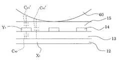
- a finger print reading device 10has such a geometry that X-axis electrodes 12 are disposed at a predetermined spacing on a substrate 11 , Y-axis electrodes 14 orthogonal to the X-axis electrodes 12 are disposed at an equal spacing through an inter-layer insulating film 13 on the X-axis electrodes 12 . Further, a surface protective film 15 composed of a dielectric substance is provided on the Y-axis electrodes 14 . Moreover, each of the X-axis electrodes 12 is connected to an X-axis driver 18 , and each of the Y-axis electrodes 14 is connected to a Y-axis driver 19 .
- a standard resolution of the fingerprint reading device 10is on the order of 300 dpi at a pitch of approximately 50 ⁇ m.
- FIGS. 2 ( a ), 2 ( b ) and 2 ( c )are schematic explanatory diagrams showing how the fingerprint is detected.
- addresses ( 1 , 1 ) ⁇ (x, y)are given to respective points of intersections thereof.
- a capacitor Cx 1is formed between a finger 60 and the X-axis electrode X 1 (FIG. 2 ( a )).
- An electrostatic capacity of this capacitor Cx 1is a total value of the X-axis electrodes X 1 extending in the longitudinal direction.
- a capacitor Cy 1is formed between the finger 60 and the Y-axis electrode Y 1 (FIG. 2 ( b )).
- An electrostatic capacity of this capacitor Cy 1is a total value of the Y-axis electrodes Y 1 extending in the longitudinal direction. These numerical values are measured with respect to the X-axis electrodes 12 and the Y-axis electrodes 14 and set as a first electrostatic capacity value.
- the X-axis electrodes X 1 ⁇ Xxare sequentially chosen for the duration of applying the predetermined voltage to the Y-axis electrode Y 1 , and for instance, a predetermined voltage is applied in sequence thereto.
- a value obtained by this operationis set as a second electrostatic capacity value.
- a mutual interferenceoccurs between the X-axis electrode X 1 and the Y-axis electrode Y 1 in the vicinity of a point-of-intersection ( 1 , 1 ), and, for example, there occurs a change such as forming a capacitor Cxy between the X-axis electrode X 1 and the Y-axis electrode Y 1 .
- a changesuch as forming a capacitor Cxy between the X-axis electrode X 1 and the Y-axis electrode Y 1 .
- an electrostatic capacity value between the point-of-intersection ( 1 , 1 ) and the finger 60changes.
- the first electrostatic capacity value and the second electrostatic capacity valuewhich have been measured with respect to the X-axis electrode X 1 and the Y-axis electrode Y 1 , differ from each other. Namely, as explained above, the capacitors Cx 1 and Cy 1 that are separately measured become capacitors Cx 1 ′ and Cy 1 ′ of which electrostatic capacities are different from each other.
- an electrostatic capacity variation value obtained by comparing the first electrostatic capacity value with the second electrostatic capacity valuedepends on an electrostatic capacity between the finger ( 60 ) and the point-of-intersection ( 1 , 1 ) between the X-axis electrode X 1 and the Y-axis electrode Y 1 , and is therefore different based on whether apart facing to the point-of-intersection ( 1 , 1 ) is a projected area or a recessed area of the fingerprint. Accordingly, if a magnitude of this variation value is obtained per point of intersection and a pattern of these variation values is formed, a fingerprint-mapped pattern is obtained, whereby the fingerprint can be read.
- a thus constructed fingerprint reading sensor 10is provided in, e.g., a liquid crystal display area on a liquid crystal panel of a liquid crystal display device, and can be easily assembled to an electronic apparatus, etc.
- the X-axis electrodes 12 , the inter-layer insulating film 13 , the Y-axis electrodes 14 and the surface protective film 15 in this casemust be all, as a matter of course, composed of transparent materials.
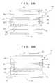
- FIG. 3shows an example in which the fingerprint reading device is provided on the liquid crystal panel.
- a liquid crystal panel 20is constructed in a way of joining a first transparent substrate 21 to a second transparent substrate 22 through a spacer 23 , and interposing a liquid crystal layer 24 therebetween. Further, transparent electrodes 25 and active elements 26 are arranged on the inner side of the first transparent substrate 21 in a two-dimensional array corresponding to pixels in a face-to-face relation with the liquid crystal layer 24 , and an orientated film 27 is provided covering these electrodes 25 and elements 26 . On the other hand, on the inner side of the second transparent substrate 22 , a common transparent electrode 28 and an oriented film 29 covering the surface thereof are provided above the liquid crystal layer 24 . Note that polarizing plates 31 , 32 are provided on the outer side of the first and second transparent substrates 21 , 22 .
- FIG. 3 ( a )shows an example where the fingerprint reading device 10 is provided on the outer side of the second transparent substrate 22 .
- FIG. 3 ( b )shows an example where the fingerprint reading device 10 is provided on the polarizing plate 32 .
- the finger print reading device 10maybe disposed, without being limited to a specific position in the plane-direction of the liquid crystal display area, at a corner or central portion of the display area, and further the whole display area may also be utilized as the fingerprint reading device.
- the fingerprint reading devicemay easily be incorporated into a variety of electronic apparatuses each having the liquid crystal display device, such as various personal computers, mobile terminals, mobile telephones, personal handyphone systems (PHS) and display-attached cards.
- liquid crystal display devicesuch as various personal computers, mobile terminals, mobile telephones, personal handyphone systems (PHS) and display-attached cards.
- PHSpersonal handyphone systems
- the electrostatic capacity type fingerprint reading sensor and the drive circuit thereofare provided on the liquid crystal panel, thereby exhibiting effects of being capable of enhancing the versatility when actually used, increasing the productivity and reducing the costs.
Landscapes
- Engineering & Computer Science (AREA)
- Human Computer Interaction (AREA)
- Physics & Mathematics (AREA)
- General Physics & Mathematics (AREA)
- Multimedia (AREA)
- Theoretical Computer Science (AREA)
- Measurement Of Length, Angles, Or The Like Using Electric Or Magnetic Means (AREA)
- Image Input (AREA)
- Measurement Of The Respiration, Hearing Ability, Form, And Blood Characteristics Of Living Organisms (AREA)
- Image Generation (AREA)
Abstract
Description
1. Field of the Invention
The present invention relates to a fingerprint reading device and to a method of use thereof.
2. Related Background Art
Some known systems for authenticating an individual for the purpose of keeping confidentiality, etc., use an ID number, a password, and so on. However, an ID is not perfect to maintain confidentiality because the ID number and password might leak out. While on the other hand, a system using a fingerprint reading device is proposed as being capable of keeping confidentiality at a much higher level.
There have been proposed electrostatic capacity type fingerprint reading devices (Japanese Patent Application Laid-Open No. Hei4-231803, etc.) for detecting a fingerprint pattern by utilizing the fact that electrostatic capacities between a group of electrodes arranged in a two-dimensional array and a finger touching [on] the electrode group through a dielectric substance layer differ corresponding to a ruggedness of the fingerprint. Some of this type of fingerprint reading devices has been utilized.
However, because the electrostatic capacity type fingerprint reading sensor in the prior art has a necessity for providing detection electrodes and active elements in a two-dimensional array, it is complicated in manufacturing and high in Cost. Further, conventionally there was not a well-designed scheme for what sort of apparatus incorporate such type of fingerprint reading device and how the fingerprint reading device is used, and very few fingerprint reading devices have been utilized.
It is a primary object of the present invention, which was devised under such circumstances, to provide a finger print reading device and a method thereof that are capable of enhancing a versatility when actually used, increasing productivity and reducing costs.
To accomplish the above object, according to a first aspect of the present invention, a fingerprint reading device comprises a fingerprint reading sensor including a group of first electrodes arranged in a plurality of lines extending in a first direction, a group of second electrodes arranged in a plurality of lines extending in a second direction intersecting the first direction above the first electrode group through an inter-layer insulating film, and a surface protective film composed of a dielectric substance provided on the second electrode group, and a drive circuit for measuring an electrostatic capacity between each of the electrodes and a fingerprint touching on the surface protective film by sequentially applying a predetermined voltage to any one group of the first electrodes and the second electrodes and at the same time sequentially applying the voltage to the other group of the electrodes, and measuring a change in the electrostatic capacity in the vicinity of a point of intersection between the first electrode and the second electrode.
According to the first aspect of the invention, the predetermined voltage is applied to every first electrode, and the pattern of the electrostatic capacities at the points of intersections are detected by scanning the second electrodes, thereby obtaining an image of the fingerprint.
According to a second aspect of the present invention, in the fingerprint reading device according to the first aspect of the invention, the drive circuit may detect, as a first electrostatic capacity value, the electrostatic capacity between each of the electrodes and the fingerprint touching on the surface protective film in a state where the voltage is applied to each electrode of the first electrode group and of the second electrode group, and further detect, as a second electrostatic capacity value, the electrostatic capacity between each of the electrodes and the fingerprint touching on the surface protective film in a state where the voltage is applied simultaneously to two electrodes passing through each point of intersection between the first electrode and the second electrode, then obtain an electrostatic capacity variation value at each point of intersection by comparing the first electrostatic capacity value with the second electrostatic capacity value, and obtain a fingerprint pattern from a pattern of the electrostatic capacity variation values.
According to the second aspect of the invention, the first electrostatic capacity value between the fingerprint and the electrode when applying the voltage solely to each of the first and second electrodes, is compared with the second electrostatic capacity value when applying the voltage simultaneously to the first and second electrodes passing through each point of intersection, thereby obtaining the electrostatic capacity variation values between the respective points of intersections and the fingerprint. A fingerprint pattern is obtained from the pattern of the electrostatic capacity variation values.
According to a third aspect of the present invention, in the fingerprint reading device according to the first or the second aspect of the invention, the fingerprint reading sensor may be transparent and provided in at least a part of the display area of the liquid crystal panel of the liquid crystal display device.
According to the third aspect of the invention, the fingerprint reading sensor is provided in superposition on the display area of the liquid crystal panel, and can be therefore mounted together with the liquid crystal panel when incorporating into an electronic apparatus, etc. This makes it feasible to save space for installing the fingerprint reading sensor.
According to a fourth aspect of the present invention, in the fingerprint reading device according to the third aspect of the invention, the fingerprint reading sensor may be provided on a surface of the polarizing plate or the transparent substrate of the liquid crystal panel.
According to the fourth aspect of the invention, the fingerprint sensor is provided on the transparent substrate or the polarizing plate and can thus be made integral with the liquid crystal panel.
According to a fifth aspect of the present invention, a fingerprint reading method comprises the steps of arranging a group of first electrodes in a plurality of lines extending in a first direction, arranging a group of second electrodes in a plurality of lines extending in a second direction intersecting the first direction above the first electrode group through an inter-layer insulating film, applying sequentially a predetermined voltage to any one group of the first electrodes and the second electrodes and at the same time sequentially applying the voltage to the other group of the electrodes by use of a fingerprint reading sensor of which a surface is provided with a surface protective film composed of a dielectric substance, and measuring a change in electrostatic capacity at a point of intersection between the first electrode and the second electrode.
According to the fifth aspect of the invention, the predetermined voltage is applied to every first electrode, and the pattern of the electrostatic capacities at the points of intersections are detected by scanning the first electrodes, thereby obtaining an image of the fingerprint.
According to a sixth aspect of the present invention, a fingerprint reading method comprises the steps of detecting, as a first electrostatic capacity value, the electrostatic capacity between each of the electrodes and the fingerprint touching on the surface protective film in a state where the voltage is applied to each electrode of the first electrode group and of the second electrode group, detecting, as a second electrostatic capacity value, the electrostatic capacity between each of the electrodes and the fingerprint touching on the surface protective film in a state where the voltage is applied simultaneously to two electrodes passing through each point of intersection between the first electrode and the second electrode, obtaining an electrostatic capacity variation value at each point of intersection by comparing the first electrostatic capacity value with the second electrostatic capacity value, and obtaining a fingerprint pattern from a pattern of the electrostatic capacity variation values.
According to the sixth aspect of the invention, the first electrostatic capacity value between the fingerprint and the electrode when applying the voltage solely to each of the first and second electrodes, is compared with the second electrostatic capacity value when applying the voltage simultaneously to the first and second electrodes passing through each point of intersection, thereby obtaining the electrostatic capacity variation values between the respective points of intersections and the fingerprint. A fingerprint pattern is obtained from the pattern of the electrostatic capacity variation values.
FIGS.1(a) is a sectional view schematically showing a configuration of a fingerprint reading device in one embodiment of the present invention; FIG.1(b) is a plan view thereof;
FIGS.2(a) through2(c) are explanatory views showing how a fingerprint is read by the fingerprint reading device in one embodiment of the present invention; and
FIGS.3(a) and3(b) are sectional views each showing a liquid crystal display device mounted with the fingerprint reading device in one embodiment of the present invention.
An embodiment of the present invention will hereinafter be described.
FIG. 1 schematically shows a configuration of a fingerprint reading device in one embodiment.
As illustrated in FIG. 1, a fingerprint reading device 10 has such a geometry thatX-axis electrodes 12 are disposed at a predetermined spacing on asubstrate 11, Y-axis electrodes 14 orthogonal to theX-axis electrodes 12 are disposed at an equal spacing through an inter-layer insulatingfilm 13 on theX-axis electrodes 12. Further, a surfaceprotective film 15 composed of a dielectric substance is provided on the Y-axis electrodes 14. Moreover, each of theX-axis electrodes 12 is connected to anX-axis driver 18, and each of the Y-axis electrodes 14 is connected to a Y-axis driver 19.
Note that a standard resolution of thefingerprint reading device 10 is on the order of 300 dpi at a pitch of approximately 50 μm.
Steps of detecting the fingerprint by use of the thus constructedfingerprint reading device 10 will be briefly explained. FIGS.2(a),2(b) and2(c) are schematic explanatory diagrams showing how the fingerprint is detected.
As shown in FIG.1(b), supposing that x-pieces of X-axis electrodes12X1˜12Xx and y-pieces of Y-axis electrodes14Y1˜14Yy are provided, addresses (1,1)˜(x, y) are given to respective points of intersections thereof.
Herein, to begin with, when theX-axis driver 18 selects the X-axis electrode X1 and applies a predetermined voltage thereto, a capacitor Cx1 is formed between afinger 60 and the X-axis electrode X1 (FIG.2(a)). An electrostatic capacity of this capacitor Cx1 is a total value of the X-axis electrodes X1 extending in the longitudinal direction. Further, when the Y-axis driver 19 selects the Y-axis electrode Y1 and applies a predetermined voltage thereto, a capacitor Cy1 is formed between thefinger 60 and the Y-axis electrode Y1 (FIG.2(b)). An electrostatic capacity of this capacitor Cy1 is a total value of the Y-axis electrodes Y1 extending in the longitudinal direction. These numerical values are measured with respect to theX-axis electrodes 12 and the Y-axis electrodes 14 and set as a first electrostatic capacity value.
On the other hand, the X-axis electrodes X1˜Xx are sequentially chosen for the duration of applying the predetermined voltage to the Y-axis electrode Y1, and for instance, a predetermined voltage is applied in sequence thereto. A value obtained by this operation is set as a second electrostatic capacity value.
At this time, if, e.g., the X-axis electrode X1 is selected, a mutual interference occurs between the X-axis electrode X1 and the Y-axis electrode Y1 in the vicinity of a point-of-intersection (1,1), and, for example, there occurs a change such as forming a capacitor Cxy between the X-axis electrode X1 and the Y-axis electrode Y1. With this change, an electrostatic capacity value between the point-of-intersection (1,1) and thefinger 60 changes. Due to this change in the electrostatic capacity value, the first electrostatic capacity value and the second electrostatic capacity value, which have been measured with respect to the X-axis electrode X1 and the Y-axis electrode Y1, differ from each other. Namely, as explained above, the capacitors Cx1 and Cy1 that are separately measured become capacitors Cx1′ and Cy1′ of which electrostatic capacities are different from each other.
Herein, an electrostatic capacity variation value obtained by comparing the first electrostatic capacity value with the second electrostatic capacity value, depends on an electrostatic capacity between the finger (60) and the point-of-intersection (1,1) between the X-axis electrode X1 and the Y-axis electrode Y1, and is therefore different based on whether apart facing to the point-of-intersection (1,1) is a projected area or a recessed area of the fingerprint. Accordingly, if a magnitude of this variation value is obtained per point of intersection and a pattern of these variation values is formed, a fingerprint-mapped pattern is obtained, whereby the fingerprint can be read.
A thus constructedfingerprint reading sensor 10 is provided in, e.g., a liquid crystal display area on a liquid crystal panel of a liquid crystal display device, and can be easily assembled to an electronic apparatus, etc. Note that theX-axis electrodes 12, the inter-layer insulatingfilm 13, the Y-axis electrodes 14 and the surfaceprotective film 15 in this case must be all, as a matter of course, composed of transparent materials.
FIG. 3 shows an example in which the fingerprint reading device is provided on the liquid crystal panel.
As illustrated in FIG. 3, aliquid crystal panel 20 is constructed in a way of joining a firsttransparent substrate 21 to a secondtransparent substrate 22 through aspacer 23, and interposing aliquid crystal layer 24 therebetween. Further,transparent electrodes 25 andactive elements 26 are arranged on the inner side of the firsttransparent substrate 21 in a two-dimensional array corresponding to pixels in a face-to-face relation with theliquid crystal layer 24, and anorientated film 27 is provided covering theseelectrodes 25 andelements 26. On the other hand, on the inner side of the secondtransparent substrate 22, a commontransparent electrode 28 and anoriented film 29 covering the surface thereof are provided above theliquid crystal layer 24. Note that polarizingplates transparent substrates
Herein, FIG.3(a) shows an example where thefingerprint reading device 10 is provided on the outer side of the secondtransparent substrate 22. FIG.3(b) shows an example where thefingerprint reading device 10 is provided on thepolarizing plate 32. The fingerprint reading device 10 maybe disposed, without being limited to a specific position in the plane-direction of the liquid crystal display area, at a corner or central portion of the display area, and further the whole display area may also be utilized as the fingerprint reading device.
The fingerprint reading device may easily be incorporated into a variety of electronic apparatuses each having the liquid crystal display device, such as various personal computers, mobile terminals, mobile telephones, personal handyphone systems (PHS) and display-attached cards.
As discussed above, according to the present invention, the electrostatic capacity type fingerprint reading sensor and the drive circuit thereof are provided on the liquid crystal panel, thereby exhibiting effects of being capable of enhancing the versatility when actually used, increasing the productivity and reducing the costs.
Claims (11)
1. A fingerprint reading device comprising: a fingerprint reading sensor having a first group of electrodes arranged in a plurality of lines extending in a first direction, a second group of electrodes arranged in a plurality of lines extending in a second direction intersecting the first direction, an insulation film provided between the first group of electrodes and the second group of electrodes, and a surface protective film formed of a dielectric substance provided over the first and second groups of electrodes, each point at which one electrode of the second group of electrodes crosses over one electrode of the first group of electrodes being a respective cell of the fingerprint reading sensor; and a drive circuit for measuring an electrostatic capacity between each of the electrodes and a finger touching the surface protective film by sequentially applying a predetermined voltage to one of the first group of electrodes and the second group of electrodes and at the same time sequentially applying the predetermined voltage to the other group of electrodes, and measuring a change in electrostatic capacity at the respective cells.
2. A fingerprint reading device according toclaim 1 ; wherein the drive circuit measures a change in the electrostatic capacity at the respective cells by detecting a first electrostatic capacity value between each of the electrodes and the finger touching the surface protective film while the voltage is individually applied to each electrode of the first electrode group and the second electrode group, detecting a second electrostatic capacity value between each of the electrodes and the finger touching the surface protective film while the voltage is applied simultaneously to two electrodes passing through each point at which a second electrode crosses over a first electrode, and obtaining an electrostatic capacity variation value at each cell by comparing the first electrostatic capacity value with the second electrostatic capacity value, and obtains a fingerprint pattern based on a pattern of the electrostatic capacity variation values at each cell.
3. A fingerprint reading device according to eitherclaim 1 orclaim 2 ; wherein the fingerprint reading sensor is transparent and is provided in a display area of a liquid crystal display panel.
4. A fingerprint reading device according toclaim 3 ; wherein the fingerprint reading sensor is provided on a surface of a polarizing plate or a transparent substrate of the liquid crystal display panel.
5. A fingerprint reading device according toclaim 1 ; wherein the first and second groups of electrodes are transparent electrodes formed on a transparent substrate of a liquid crystal panel.
6. A fingerprint reading device according toclaim 1 ; wherein the first and second groups of electrodes of the fingerprint reading sensor are transparent.
7. A fingerprint reading device according toclaim 1 ; wherein the fingerprint reading sensor is provided in a display area of a liquid crystal display panel.
8. A fingerprint reading method comprising the steps of:
arranging a group of first electrodes in a plurality of lines extending in a first direction;
arranging a group of second electrodes in a plurality of lines extending in a second direction intersecting the first direction and above the first electrode group through an inter-layer insulating film;
arranging a surface protective film formed of a dielectric substance on the group of second electrodes;
sequentially applying a predetermined voltage to one of the first group of electrodes and the second group of electrodes and at the same time sequentially applying the predetermined voltage to the other group of electrodes; and
measuring a change in electrostatic capacity at a point where a second electrode crosses over a first electrode.
9. A fingerprint reading method comprising the steps of:
arranging a group of first electrodes in a plurality of lines extending in a first direction;
providing an interlayer insulating film on the first group of electrodes;
arranging a group of second electrodes in a plurality of lines extending in a second direction intersecting the first direction and above the interlayer insulating film to form a fingerprint reading sensor having an array of cells each comprising a point where a second electrode crosses over a first electrode;
providing an interlayer insulating film between the group of first electrodes and the group of second electrodes;
providing a surface protective film formed of a dielectric substance on the group of second electrodes;
detecting a first electrostatic capacity value between each of the electrodes and a finger touching the surface protective film while a voltage is individually applied to each electrode of the first electrode group and the second electrode group;
detecting a second electrostatic capacity value between each of the electrodes and the finger touching the surface protective film while a voltage is simultaneously applied to two electrodes passing through the respective cells;
obtaining an electrostatic capacity variation value at each cell by comparing the first electrostatic capacity value with the second electrostatic capacity value; and
obtaining a fingerprint pattern from a pattern of the electrostatic capacity variation values at each cell.
10. A fingerprint reading device comprising: a fingerprint reading sensor having a first group of electrodes arranged in a plurality of lines extending in a first direction, a second group of electrodes arranged in a plurality of lines extending in a second direction intersecting the first direction, an insulation film provided between the first group of electrodes and the second group of electrodes, and a surface protective film formed of a dielectric substance provided over the first and second groups of electrodes, each point at which one electrode of the second group of electrodes crosses over one electrode of the first group of electrodes being a respective cell of the fingerprint reading sensor; and a drive circuit for driving the fingerprint reading sensor to obtain a fingerprint pattern by measuring a change in the electrostatic capacity at the respective cells by detecting a first electrostatic capacity value between each of the electrodes and a finger touching the surface protective film while a predetermined voltage is individually applied to each electrode of the first electrode group and the second electrode group, detecting a second electrostatic capacity value between each of the electrodes and the finger touching the surface protective film while the predetermined voltage is applied simultaneously to two electrodes passing through each point at which a second electrode crosses over a first electrode, obtaining an electrostatic capacity variation value at each cell by comparing the first electrostatic capacity value with the second electrostatic capacity value, and obtaining the fingerprint pattern based on a pattern of the electrostatic capacity variation values at the respective cells.
11. A fingerprint reading device according toclaim 10 ; wherein the fingerprint reading sensor is transparent and is provided in a display area of a liquid crystal display panel.
Applications Claiming Priority (2)
| Application Number | Priority Date | Filing Date | Title |
|---|---|---|---|
| JP22845899AJP4233698B2 (en) | 1999-08-12 | 1999-08-12 | Fingerprint reading apparatus and method |
| JP11-228458 | 1999-08-12 |
Publications (1)
| Publication Number | Publication Date |
|---|---|
| US6462563B1true US6462563B1 (en) | 2002-10-08 |
Family
ID=16876814
Family Applications (1)
| Application Number | Title | Priority Date | Filing Date |
|---|---|---|---|
| US09/638,261Expired - LifetimeUS6462563B1 (en) | 1999-08-12 | 2000-08-11 | Fingerprint reading device and method thereof |
Country Status (3)
| Country | Link |
|---|---|
| US (1) | US6462563B1 (en) |
| JP (1) | JP4233698B2 (en) |
| CN (1) | CN1161737C (en) |
Cited By (24)
| Publication number | Priority date | Publication date | Assignee | Title |
|---|---|---|---|---|
| US20020090211A1 (en)* | 2001-01-09 | 2002-07-11 | Yukito Kawahara | Apparatus for implementing readout of fingerprint |
| US20020150284A1 (en)* | 2001-04-16 | 2002-10-17 | Hajimu Iwai | Fingerprint recognition device and fingerprint recognition method |
| US20040190761A1 (en)* | 2003-03-05 | 2004-09-30 | Ju-Hyeon Lee | Apparatus for fingerprint analysis using current detection |
| US6826000B2 (en) | 2001-09-17 | 2004-11-30 | Secugen Corporation | Optical fingerprint acquisition apparatus |
| US6870946B1 (en) | 1998-08-06 | 2005-03-22 | Secugen Corporation | Compact optical fingerprint capturing and recognition system |
| EP1536368A1 (en)* | 2003-11-25 | 2005-06-01 | Alps Electric Co., Ltd. | Capacitance detecting circuit and method, and fingerprint sensor using the same |
| US6917695B2 (en) | 1998-11-12 | 2005-07-12 | Secugen Corporation | High contrast, low distortion optical acquisition system for image capturing |
| US20050226476A1 (en)* | 2003-08-05 | 2005-10-13 | Takeshi Funahashi | Fingerprint matching processor |
| US20050253598A1 (en)* | 2004-05-12 | 2005-11-17 | Alps Electric Co., Ltd. | Capacitance detection-type sensor |
| US20060119369A1 (en)* | 2004-12-03 | 2006-06-08 | Alps Electric Co., Ltd. | Capacity detecting sensor |
| US20070052428A1 (en)* | 2003-05-07 | 2007-03-08 | Koninklijke Philips Electronics N.V. | Object sensing |
| US20070062852A1 (en)* | 2005-08-11 | 2007-03-22 | N-Trig Ltd. | Apparatus for Object Information Detection and Methods of Using Same |
| US20070208962A1 (en)* | 2001-01-22 | 2007-09-06 | Ati International, Srl | Apparatus and method for reducing power consumption of a processor by estimating engine load |
| EP1521203A3 (en)* | 2003-10-02 | 2009-05-27 | Alps Electric Co., Ltd. | Capacitance detector circuit, capacitance detector method and fingerprint sensor using the same |
| US9348477B2 (en) | 2005-11-15 | 2016-05-24 | Synaptics Incorporated | Methods and systems for detecting a position-based attribute of an object using digital codes |
| US9465491B2 (en) | 2010-11-02 | 2016-10-11 | Atmel Corporation | Method for forming a capacitive touch sensor for identifying a fingerprint |
| US20170076131A1 (en)* | 2015-09-16 | 2017-03-16 | Samsung Electronics Co., Ltd. | Fingerprint sensor |
| TWI596549B (en)* | 2016-07-25 | 2017-08-21 | Superc-Touch Coporation | Fingerprint recognition apparatus |
| US20170344790A1 (en)* | 2016-05-30 | 2017-11-30 | Kyocera Corporation | Wiring board for fingerprint sensor |
| US9886614B2 (en) | 2015-09-25 | 2018-02-06 | Kyocera Corporation | Wiring board for fingerprint sensor |
| US9928400B2 (en) | 2015-09-25 | 2018-03-27 | Kyocera Corporation | Wiring board for fingerprint sensor |
| US10108839B2 (en) | 2016-06-27 | 2018-10-23 | Japan Display Inc. | Display device |
| US10282029B2 (en) | 2016-07-11 | 2019-05-07 | Japan Display Inc. | Cover member and display apparatus |
| US20240061537A1 (en)* | 2012-10-14 | 2024-02-22 | Synaptics Incorporated | Fingerprint sensor and button combinations and methods of making same |
Families Citing this family (14)
| Publication number | Priority date | Publication date | Assignee | Title |
|---|---|---|---|---|
| JP2004138416A (en)* | 2002-10-16 | 2004-05-13 | Nihon Kaiheiki Industry Co Ltd | Pressure-sensitive fingerprint sensor |
| KR100526488B1 (en)* | 2002-11-26 | 2005-11-08 | 재단법인서울대학교산학협력재단 | Apparatus for sensing the touch status |
| JP4440603B2 (en)* | 2003-11-06 | 2010-03-24 | アルプス電気株式会社 | Capacitance detection circuit, detection method, and fingerprint sensor using the same |
| CN1308886C (en)* | 2004-02-05 | 2007-04-04 | 祥群科技股份有限公司 | Capacitive pressure sensing element structure and manufacturing method |
| JP4447952B2 (en)* | 2004-04-07 | 2010-04-07 | アルプス電気株式会社 | Charge detection circuit and fingerprint sensor using the same |
| KR100627174B1 (en) | 2005-04-11 | 2006-09-25 | 주식회사 맥퀸트전자 | Contact sensing sensor by capacitor with distributed electrodes |
| CN103927468B (en)* | 2013-12-31 | 2017-08-11 | 上海天马微电子有限公司 | Fingerprint identification module and display device |
| CN103870015A (en)* | 2014-03-20 | 2014-06-18 | 汕头超声显示器技术有限公司 | Manufacturing method of capacitive touch screen |
| CN104881238A (en) | 2015-06-25 | 2015-09-02 | 京东方科技集团股份有限公司 | Touch control display device and touch control method thereof |
| CN106529439A (en)* | 2016-10-31 | 2017-03-22 | 北京小米移动软件有限公司 | Protective film, display substrate and electronic equipment |
| CN106778508B (en)* | 2016-11-22 | 2018-09-04 | 维沃移动通信有限公司 | A kind of fingerprint identification method and mobile terminal |
| JP2019121054A (en)* | 2017-12-28 | 2019-07-22 | 株式会社東海理化電機製作所 | Fingerprint authentication device |
| CN108491800B (en)* | 2018-03-26 | 2021-03-23 | 昆山龙腾光电股份有限公司 | Palm feature recognition device and palm feature recognition method |
| CN112395926A (en)* | 2019-08-19 | 2021-02-23 | 北京小米移动软件有限公司 | Screen module, fingerprint detection method and device and electronic equipment |
Citations (5)
| Publication number | Priority date | Publication date | Assignee | Title |
|---|---|---|---|---|
| US4353056A (en)* | 1980-06-05 | 1982-10-05 | Siemens Corporation | Capacitive fingerprint sensor |
| US5461319A (en)* | 1992-12-28 | 1995-10-24 | Peters; Randall D. | Symmetric differential capacitance transducer employing cross coupled conductive plates to form equipotential pairs |
| US5583303A (en)* | 1992-09-18 | 1996-12-10 | Incontrol Solutions, Inc. | Transducer array |
| US6072318A (en)* | 1996-10-11 | 2000-06-06 | Brown & Sharpe Tesa S.A. | Capacitive device for measuring dimension |
| US6114862A (en)* | 1996-02-14 | 2000-09-05 | Stmicroelectronics, Inc. | Capacitive distance sensor |
- 1999
- 1999-08-12JPJP22845899Apatent/JP4233698B2/ennot_activeExpired - Fee Related
- 2000
- 2000-08-11USUS09/638,261patent/US6462563B1/ennot_activeExpired - Lifetime
- 2000-08-11CNCNB001226355Apatent/CN1161737C/ennot_activeExpired - Lifetime
Patent Citations (5)
| Publication number | Priority date | Publication date | Assignee | Title |
|---|---|---|---|---|
| US4353056A (en)* | 1980-06-05 | 1982-10-05 | Siemens Corporation | Capacitive fingerprint sensor |
| US5583303A (en)* | 1992-09-18 | 1996-12-10 | Incontrol Solutions, Inc. | Transducer array |
| US5461319A (en)* | 1992-12-28 | 1995-10-24 | Peters; Randall D. | Symmetric differential capacitance transducer employing cross coupled conductive plates to form equipotential pairs |
| US6114862A (en)* | 1996-02-14 | 2000-09-05 | Stmicroelectronics, Inc. | Capacitive distance sensor |
| US6072318A (en)* | 1996-10-11 | 2000-06-06 | Brown & Sharpe Tesa S.A. | Capacitive device for measuring dimension |
Non-Patent Citations (2)
| Title |
|---|
| A single chip fingerprint sensor and identifier, IEEE, Dec. 1999.* |
| Direct contact 500dppi fingerprint sensor, IEEE, Jan. 1998.** |
Cited By (41)
| Publication number | Priority date | Publication date | Assignee | Title |
|---|---|---|---|---|
| US6870946B1 (en) | 1998-08-06 | 2005-03-22 | Secugen Corporation | Compact optical fingerprint capturing and recognition system |
| US6917695B2 (en) | 1998-11-12 | 2005-07-12 | Secugen Corporation | High contrast, low distortion optical acquisition system for image capturing |
| US20020090211A1 (en)* | 2001-01-09 | 2002-07-11 | Yukito Kawahara | Apparatus for implementing readout of fingerprint |
| US20070208962A1 (en)* | 2001-01-22 | 2007-09-06 | Ati International, Srl | Apparatus and method for reducing power consumption of a processor by estimating engine load |
| US20020150284A1 (en)* | 2001-04-16 | 2002-10-17 | Hajimu Iwai | Fingerprint recognition device and fingerprint recognition method |
| US6826000B2 (en) | 2001-09-17 | 2004-11-30 | Secugen Corporation | Optical fingerprint acquisition apparatus |
| US20040190761A1 (en)* | 2003-03-05 | 2004-09-30 | Ju-Hyeon Lee | Apparatus for fingerprint analysis using current detection |
| US20070052428A1 (en)* | 2003-05-07 | 2007-03-08 | Koninklijke Philips Electronics N.V. | Object sensing |
| US7560938B2 (en)* | 2003-05-07 | 2009-07-14 | Koninklijke Philips Electronics N.V. | Object sensing |
| US8175344B2 (en)* | 2003-08-05 | 2012-05-08 | Sony Corporation | Fingerprint matching processor |
| US20050226476A1 (en)* | 2003-08-05 | 2005-10-13 | Takeshi Funahashi | Fingerprint matching processor |
| EP1521203A3 (en)* | 2003-10-02 | 2009-05-27 | Alps Electric Co., Ltd. | Capacitance detector circuit, capacitance detector method and fingerprint sensor using the same |
| US20060158202A1 (en)* | 2003-11-25 | 2006-07-20 | Alps Electric Co., Ltd. | Capacitance detecting circuit and method, and fingerprint sensor using the same |
| US7084645B1 (en) | 2003-11-25 | 2006-08-01 | Alps Electric Co., Ltd. | Capacitance detecting circuit and method, and fingerprint sensor using the same |
| EP1536368A1 (en)* | 2003-11-25 | 2005-06-01 | Alps Electric Co., Ltd. | Capacitance detecting circuit and method, and fingerprint sensor using the same |
| US20050253598A1 (en)* | 2004-05-12 | 2005-11-17 | Alps Electric Co., Ltd. | Capacitance detection-type sensor |
| US20060119369A1 (en)* | 2004-12-03 | 2006-06-08 | Alps Electric Co., Ltd. | Capacity detecting sensor |
| US8931780B2 (en) | 2005-08-11 | 2015-01-13 | N-Trig Ltd. | Apparatus for object information detection and methods of using same |
| US7902840B2 (en)* | 2005-08-11 | 2011-03-08 | N-Trig Ltd. | Apparatus for object information detection and methods of using same |
| US20090322352A1 (en)* | 2005-08-11 | 2009-12-31 | N-Trig Ltd. | Apparatus for object information detection and methods of using same |
| US20070062852A1 (en)* | 2005-08-11 | 2007-03-22 | N-Trig Ltd. | Apparatus for Object Information Detection and Methods of Using Same |
| US9435628B2 (en) | 2005-08-11 | 2016-09-06 | Microsoft Technology Licensing, Llc | Apparatus for object information detection and methods of using same |
| US9618316B2 (en) | 2005-08-11 | 2017-04-11 | Microsoft Technology Licensing, Llc | Apparatus for object information detection and methods of using same |
| US9348477B2 (en) | 2005-11-15 | 2016-05-24 | Synaptics Incorporated | Methods and systems for detecting a position-based attribute of an object using digital codes |
| US9696863B2 (en) | 2005-11-15 | 2017-07-04 | Synaptics Incorporated | Methods and systems for detecting a position-based attribute of an object using digital codes |
| US9465491B2 (en) | 2010-11-02 | 2016-10-11 | Atmel Corporation | Method for forming a capacitive touch sensor for identifying a fingerprint |
| US12429988B2 (en)* | 2012-10-14 | 2025-09-30 | Synaptics Incorporated | Fingerprint sensor and button combinations and methods of making same |
| US20240061537A1 (en)* | 2012-10-14 | 2024-02-22 | Synaptics Incorporated | Fingerprint sensor and button combinations and methods of making same |
| US10121044B2 (en)* | 2015-09-16 | 2018-11-06 | Samsung Electronics Co., Ltd. | Fingerprint sensor |
| US20170076131A1 (en)* | 2015-09-16 | 2017-03-16 | Samsung Electronics Co., Ltd. | Fingerprint sensor |
| US9886614B2 (en) | 2015-09-25 | 2018-02-06 | Kyocera Corporation | Wiring board for fingerprint sensor |
| US9928400B2 (en) | 2015-09-25 | 2018-03-27 | Kyocera Corporation | Wiring board for fingerprint sensor |
| US10089513B2 (en)* | 2016-05-30 | 2018-10-02 | Kyocera Corporation | Wiring board for fingerprint sensor |
| US20170344790A1 (en)* | 2016-05-30 | 2017-11-30 | Kyocera Corporation | Wiring board for fingerprint sensor |
| US10108839B2 (en) | 2016-06-27 | 2018-10-23 | Japan Display Inc. | Display device |
| US10860830B2 (en) | 2016-06-27 | 2020-12-08 | Japan Display Inc. | Display device |
| US10282029B2 (en) | 2016-07-11 | 2019-05-07 | Japan Display Inc. | Cover member and display apparatus |
| US10635238B2 (en) | 2016-07-11 | 2020-04-28 | Japan Display Inc. | Cover member and display apparatus |
| US11036332B2 (en) | 2016-07-11 | 2021-06-15 | Japan Display Inc. | Cover member and display apparatus |
| US10325140B2 (en)* | 2016-07-25 | 2019-06-18 | Superc-Touch Corporation | Fingerprint identification apparatus |
| TWI596549B (en)* | 2016-07-25 | 2017-08-21 | Superc-Touch Coporation | Fingerprint recognition apparatus |
Also Published As
| Publication number | Publication date |
|---|---|
| CN1161737C (en) | 2004-08-11 |
| JP4233698B2 (en) | 2009-03-04 |
| JP2001046359A (en) | 2001-02-20 |
| CN1284706A (en) | 2001-02-21 |
Similar Documents
| Publication | Publication Date | Title |
|---|---|---|
| US6462563B1 (en) | Fingerprint reading device and method thereof | |
| US6401551B1 (en) | Fingerprint reading device | |
| US6862942B2 (en) | Surface pressure distribution sensor | |
| US11347357B2 (en) | Electronic device | |
| US10338738B2 (en) | Touch display device and method for driving the same | |
| US9207797B2 (en) | Flat panel display screen operable for touch position prediction methods | |
| CN106650564B (en) | Capacitive sensor and method of making a capacitive sensor | |
| CN106502466B (en) | Touch device, electronic equipment and manufacturing method | |
| JPH0797057B2 (en) | Surface pressure distribution detection element | |
| US11281327B2 (en) | Touch substrate, method of driving the same and touch display device | |
| US20080105936A1 (en) | Surface pressure distribution sensor | |
| US10910168B2 (en) | Electronic device | |
| US11379074B2 (en) | Pad electrode part and touch sensor therewith | |
| WO2009038277A1 (en) | Resistive touch screen which can identify multi-touch | |
| CN107728356A (en) | Embedded touch liquid crystal display panel and embedded touch liquid crystal display die set | |
| EP3951565B1 (en) | Touch screen, touch display screen, and display apparatus | |
| US20210271344A1 (en) | Touch substrate and touch control display apparatus | |
| JP4424982B2 (en) | Touch panel and manufacturing method thereof | |
| US10656744B2 (en) | Thin film transistor array substrate and touch display panel using same | |
| US20120013593A1 (en) | Display device | |
| CA3049673C (en) | Coated printed electronic devices exhibiting improved yield | |
| CN113536988A (en) | Ultrasonic fingerprint identification module and detection method thereof, and display module | |
| CN115100962B (en) | Display panel and display device | |
| US11836315B2 (en) | Electronic device for identifying touch position, touch system including electronic device, and operation method thereof | |
| JPS63234315A (en) | Coordinate input/display device |
Legal Events
| Date | Code | Title | Description |
|---|---|---|---|
| AS | Assignment | Owner name:SEIKO INSTRUMENTS INC., JAPAN Free format text:ASSIGNMENT OF ASSIGNORS INTEREST;ASSIGNORS:KAWAHARA, YUKITO;FUJITA, HIROYUKI;MATSUHIRA, TSUTOMU;REEL/FRAME:013201/0343 Effective date:20020812 | |
| STCF | Information on status: patent grant | Free format text:PATENTED CASE | |
| FPAY | Fee payment | Year of fee payment:4 | |
| AS | Assignment | Owner name:SAGEM SA, FRANCE Free format text:MERGER;ASSIGNOR:SFIM INDUSTRIES;REEL/FRAME:021952/0067 Effective date:20000101 | |
| FPAY | Fee payment | Year of fee payment:8 | |
| FPAY | Fee payment | Year of fee payment:12 | |
| AS | Assignment | Owner name:SII SEMICONDUCTOR CORPORATION, JAPAN Free format text:ASSIGNMENT OF ASSIGNORS INTEREST;ASSIGNOR:SEIKO INSTRUMENTS INC.;REEL/FRAME:038058/0892 Effective date:20160105 | |
| AS | Assignment | Owner name:ABLIC INC., JAPAN Free format text:CHANGE OF NAME;ASSIGNOR:SII SEMICONDUCTOR CORPORATION;REEL/FRAME:045567/0927 Effective date:20180105 |