US6462310B1 - Hot wall rapid thermal processor - Google Patents
Hot wall rapid thermal processorDownload PDFInfo
- Publication number
- US6462310B1 US6462310B1US09/638,113US63811300AUS6462310B1US 6462310 B1US6462310 B1US 6462310B1US 63811300 AUS63811300 AUS 63811300AUS 6462310 B1US6462310 B1US 6462310B1
- Authority
- US
- United States
- Prior art keywords
- fluid
- wafer
- chamber
- heating
- heating chamber
- Prior art date
- Legal status (The legal status is an assumption and is not a legal conclusion. Google has not performed a legal analysis and makes no representation as to the accuracy of the status listed.)
- Expired - Fee Related
Links
- 238000010438heat treatmentMethods0.000claimsabstractdescription422
- 238000001816coolingMethods0.000claimsabstractdescription178
- 235000012431wafersNutrition0.000claimsdescription442
- 239000012530fluidSubstances0.000claimsdescription353
- 238000009826distributionMethods0.000claimsdescription83
- 238000012545processingMethods0.000claimsdescription68
- 239000012809cooling fluidSubstances0.000claimsdescription30
- 238000000034methodMethods0.000claimsdescription25
- 239000007789gasSubstances0.000claimsdescription22
- 239000000463materialSubstances0.000claimsdescription19
- 230000008569processEffects0.000claimsdescription15
- VYPSYNLAJGMNEJ-UHFFFAOYSA-Nsilicon dioxideInorganic materialsO=[Si]=OVYPSYNLAJGMNEJ-UHFFFAOYSA-N0.000claimsdescription14
- 230000000295complement effectEffects0.000claimsdescription10
- 239000012212insulatorSubstances0.000claimsdescription10
- 239000010453quartzSubstances0.000claimsdescription8
- 238000010926purgeMethods0.000claimsdescription7
- 230000003750conditioning effectEffects0.000claimsdescription5
- 230000000694effectsEffects0.000description60
- 238000011282treatmentMethods0.000description21
- 238000002955isolationMethods0.000description20
- 230000002093peripheral effectEffects0.000description19
- 238000012546transferMethods0.000description14
- 230000008901benefitEffects0.000description9
- 230000004888barrier functionEffects0.000description8
- 230000004907fluxEffects0.000description8
- 230000005855radiationEffects0.000description8
- HBMJWWWQQXIZIP-UHFFFAOYSA-Nsilicon carbideChemical compound[Si+]#[C-]HBMJWWWQQXIZIP-UHFFFAOYSA-N0.000description8
- 229910010271silicon carbideInorganic materials0.000description8
- XUIMIQQOPSSXEZ-UHFFFAOYSA-NSiliconChemical compound[Si]XUIMIQQOPSSXEZ-UHFFFAOYSA-N0.000description5
- 230000000903blocking effectEffects0.000description5
- 239000005350fused silica glassSubstances0.000description5
- 230000003993interactionEffects0.000description5
- 229910052710siliconInorganic materials0.000description5
- 239000010703siliconSubstances0.000description5
- IJGRMHOSHXDMSA-UHFFFAOYSA-NAtomic nitrogenChemical compoundN#NIJGRMHOSHXDMSA-UHFFFAOYSA-N0.000description4
- 238000004891communicationMethods0.000description4
- 238000013461designMethods0.000description4
- 230000007246mechanismEffects0.000description4
- XLYOFNOQVPJJNP-UHFFFAOYSA-NwaterSubstancesOXLYOFNOQVPJJNP-UHFFFAOYSA-N0.000description4
- 238000000137annealingMethods0.000description3
- 238000004519manufacturing processMethods0.000description3
- 230000002829reductive effectEffects0.000description3
- 230000000717retained effectEffects0.000description3
- 230000006641stabilisationEffects0.000description3
- 238000011105stabilizationMethods0.000description3
- 230000008646thermal stressEffects0.000description3
- 238000003466weldingMethods0.000description3
- 238000010521absorption reactionMethods0.000description2
- 238000006073displacement reactionMethods0.000description2
- 238000009413insulationMethods0.000description2
- 239000007788liquidSubstances0.000description2
- 238000012986modificationMethods0.000description2
- 230000004048modificationEffects0.000description2
- 229910052757nitrogenInorganic materials0.000description2
- 230000003647oxidationEffects0.000description2
- 238000007254oxidation reactionMethods0.000description2
- 239000004065semiconductorSubstances0.000description2
- 230000035882stressEffects0.000description2
- -1A12O3Substances0.000description1
- OKTJSMMVPCPJKN-UHFFFAOYSA-NCarbonChemical compound[C]OKTJSMMVPCPJKN-UHFFFAOYSA-N0.000description1
- RYGMFSIKBFXOCR-UHFFFAOYSA-NCopperChemical compound[Cu]RYGMFSIKBFXOCR-UHFFFAOYSA-N0.000description1
- 229910052581Si3N4Inorganic materials0.000description1
- 230000002411adverseEffects0.000description1
- 229910052782aluminiumInorganic materials0.000description1
- XAGFODPZIPBFFR-UHFFFAOYSA-NaluminiumChemical compound[Al]XAGFODPZIPBFFR-UHFFFAOYSA-N0.000description1
- 238000013459approachMethods0.000description1
- 239000000919ceramicSubstances0.000description1
- 238000005229chemical vapour depositionMethods0.000description1
- 238000004140cleaningMethods0.000description1
- 229910052802copperInorganic materials0.000description1
- 239000010949copperSubstances0.000description1
- PMHQVHHXPFUNSP-UHFFFAOYSA-Mcopper(1+);methylsulfanylmethane;bromideChemical compoundBr[Cu].CSCPMHQVHHXPFUNSP-UHFFFAOYSA-M0.000description1
- 239000013078crystalSubstances0.000description1
- 230000003111delayed effectEffects0.000description1
- 238000000151depositionMethods0.000description1
- 230000008021depositionEffects0.000description1
- 230000009977dual effectEffects0.000description1
- 239000012636effectorSubstances0.000description1
- 229910002804graphiteInorganic materials0.000description1
- 239000010439graphiteSubstances0.000description1
- 230000000670limiting effectEffects0.000description1
- 230000014759maintenance of locationEffects0.000description1
- 229910052751metalInorganic materials0.000description1
- 239000002184metalSubstances0.000description1
- 238000009828non-uniform distributionMethods0.000description1
- 230000036961partial effectEffects0.000description1
- 230000009467reductionEffects0.000description1
- 238000002310reflectometryMethods0.000description1
- 230000000284resting effectEffects0.000description1
- 230000002441reversible effectEffects0.000description1
- HQVNEWCFYHHQES-UHFFFAOYSA-Nsilicon nitrideChemical compoundN12[Si]34N5[Si]62N3[Si]51N64HQVNEWCFYHHQES-UHFFFAOYSA-N0.000description1
- 239000007787solidSubstances0.000description1
- 229910001220stainless steelInorganic materials0.000description1
- 239000010935stainless steelSubstances0.000description1
- 239000000126substanceSubstances0.000description1
- 239000000758substrateSubstances0.000description1
- 238000002230thermal chemical vapour depositionMethods0.000description1
- 238000005382thermal cyclingMethods0.000description1
- 238000009827uniform distributionMethods0.000description1
Images


Classifications
- C—CHEMISTRY; METALLURGY
- C23—COATING METALLIC MATERIAL; COATING MATERIAL WITH METALLIC MATERIAL; CHEMICAL SURFACE TREATMENT; DIFFUSION TREATMENT OF METALLIC MATERIAL; COATING BY VACUUM EVAPORATION, BY SPUTTERING, BY ION IMPLANTATION OR BY CHEMICAL VAPOUR DEPOSITION, IN GENERAL; INHIBITING CORROSION OF METALLIC MATERIAL OR INCRUSTATION IN GENERAL
- C23C—COATING METALLIC MATERIAL; COATING MATERIAL WITH METALLIC MATERIAL; SURFACE TREATMENT OF METALLIC MATERIAL BY DIFFUSION INTO THE SURFACE, BY CHEMICAL CONVERSION OR SUBSTITUTION; COATING BY VACUUM EVAPORATION, BY SPUTTERING, BY ION IMPLANTATION OR BY CHEMICAL VAPOUR DEPOSITION, IN GENERAL
- C23C16/00—Chemical coating by decomposition of gaseous compounds, without leaving reaction products of surface material in the coating, i.e. chemical vapour deposition [CVD] processes
- C23C16/44—Chemical coating by decomposition of gaseous compounds, without leaving reaction products of surface material in the coating, i.e. chemical vapour deposition [CVD] processes characterised by the method of coating
- C23C16/46—Chemical coating by decomposition of gaseous compounds, without leaving reaction products of surface material in the coating, i.e. chemical vapour deposition [CVD] processes characterised by the method of coating characterised by the method used for heating the substrate
- C23C16/463—Cooling of the substrate
- C—CHEMISTRY; METALLURGY
- C23—COATING METALLIC MATERIAL; COATING MATERIAL WITH METALLIC MATERIAL; CHEMICAL SURFACE TREATMENT; DIFFUSION TREATMENT OF METALLIC MATERIAL; COATING BY VACUUM EVAPORATION, BY SPUTTERING, BY ION IMPLANTATION OR BY CHEMICAL VAPOUR DEPOSITION, IN GENERAL; INHIBITING CORROSION OF METALLIC MATERIAL OR INCRUSTATION IN GENERAL
- C23C—COATING METALLIC MATERIAL; COATING MATERIAL WITH METALLIC MATERIAL; SURFACE TREATMENT OF METALLIC MATERIAL BY DIFFUSION INTO THE SURFACE, BY CHEMICAL CONVERSION OR SUBSTITUTION; COATING BY VACUUM EVAPORATION, BY SPUTTERING, BY ION IMPLANTATION OR BY CHEMICAL VAPOUR DEPOSITION, IN GENERAL
- C23C16/00—Chemical coating by decomposition of gaseous compounds, without leaving reaction products of surface material in the coating, i.e. chemical vapour deposition [CVD] processes
- C23C16/44—Chemical coating by decomposition of gaseous compounds, without leaving reaction products of surface material in the coating, i.e. chemical vapour deposition [CVD] processes characterised by the method of coating
- C23C16/455—Chemical coating by decomposition of gaseous compounds, without leaving reaction products of surface material in the coating, i.e. chemical vapour deposition [CVD] processes characterised by the method of coating characterised by the method used for introducing gases into reaction chamber or for modifying gas flows in reaction chamber
- C—CHEMISTRY; METALLURGY
- C23—COATING METALLIC MATERIAL; COATING MATERIAL WITH METALLIC MATERIAL; CHEMICAL SURFACE TREATMENT; DIFFUSION TREATMENT OF METALLIC MATERIAL; COATING BY VACUUM EVAPORATION, BY SPUTTERING, BY ION IMPLANTATION OR BY CHEMICAL VAPOUR DEPOSITION, IN GENERAL; INHIBITING CORROSION OF METALLIC MATERIAL OR INCRUSTATION IN GENERAL
- C23C—COATING METALLIC MATERIAL; COATING MATERIAL WITH METALLIC MATERIAL; SURFACE TREATMENT OF METALLIC MATERIAL BY DIFFUSION INTO THE SURFACE, BY CHEMICAL CONVERSION OR SUBSTITUTION; COATING BY VACUUM EVAPORATION, BY SPUTTERING, BY ION IMPLANTATION OR BY CHEMICAL VAPOUR DEPOSITION, IN GENERAL
- C23C16/00—Chemical coating by decomposition of gaseous compounds, without leaving reaction products of surface material in the coating, i.e. chemical vapour deposition [CVD] processes
- C23C16/44—Chemical coating by decomposition of gaseous compounds, without leaving reaction products of surface material in the coating, i.e. chemical vapour deposition [CVD] processes characterised by the method of coating
- C23C16/458—Chemical coating by decomposition of gaseous compounds, without leaving reaction products of surface material in the coating, i.e. chemical vapour deposition [CVD] processes characterised by the method of coating characterised by the method used for supporting substrates in the reaction chamber
- C23C16/4582—Rigid and flat substrates, e.g. plates or discs
- C23C16/4583—Rigid and flat substrates, e.g. plates or discs the substrate being supported substantially horizontally
- C23C16/4584—Rigid and flat substrates, e.g. plates or discs the substrate being supported substantially horizontally the substrate being rotated
- C—CHEMISTRY; METALLURGY
- C30—CRYSTAL GROWTH
- C30B—SINGLE-CRYSTAL GROWTH; UNIDIRECTIONAL SOLIDIFICATION OF EUTECTIC MATERIAL OR UNIDIRECTIONAL DEMIXING OF EUTECTOID MATERIAL; REFINING BY ZONE-MELTING OF MATERIAL; PRODUCTION OF A HOMOGENEOUS POLYCRYSTALLINE MATERIAL WITH DEFINED STRUCTURE; SINGLE CRYSTALS OR HOMOGENEOUS POLYCRYSTALLINE MATERIAL WITH DEFINED STRUCTURE; AFTER-TREATMENT OF SINGLE CRYSTALS OR A HOMOGENEOUS POLYCRYSTALLINE MATERIAL WITH DEFINED STRUCTURE; APPARATUS THEREFOR
- C30B25/00—Single-crystal growth by chemical reaction of reactive gases, e.g. chemical vapour-deposition growth
- C30B25/02—Epitaxial-layer growth
- C30B25/10—Heating of the reaction chamber or the substrate
- C—CHEMISTRY; METALLURGY
- C30—CRYSTAL GROWTH
- C30B—SINGLE-CRYSTAL GROWTH; UNIDIRECTIONAL SOLIDIFICATION OF EUTECTIC MATERIAL OR UNIDIRECTIONAL DEMIXING OF EUTECTOID MATERIAL; REFINING BY ZONE-MELTING OF MATERIAL; PRODUCTION OF A HOMOGENEOUS POLYCRYSTALLINE MATERIAL WITH DEFINED STRUCTURE; SINGLE CRYSTALS OR HOMOGENEOUS POLYCRYSTALLINE MATERIAL WITH DEFINED STRUCTURE; AFTER-TREATMENT OF SINGLE CRYSTALS OR A HOMOGENEOUS POLYCRYSTALLINE MATERIAL WITH DEFINED STRUCTURE; APPARATUS THEREFOR
- C30B25/00—Single-crystal growth by chemical reaction of reactive gases, e.g. chemical vapour-deposition growth
- C30B25/02—Epitaxial-layer growth
- C30B25/14—Feed and outlet means for the gases; Modifying the flow of the reactive gases
- H—ELECTRICITY
- H01—ELECTRIC ELEMENTS
- H01L—SEMICONDUCTOR DEVICES NOT COVERED BY CLASS H10
- H01L21/00—Processes or apparatus adapted for the manufacture or treatment of semiconductor or solid state devices or of parts thereof
- H01L21/67—Apparatus specially adapted for handling semiconductor or electric solid state devices during manufacture or treatment thereof; Apparatus specially adapted for handling wafers during manufacture or treatment of semiconductor or electric solid state devices or components ; Apparatus not specifically provided for elsewhere
- H01L21/67005—Apparatus not specifically provided for elsewhere
- H01L21/67011—Apparatus for manufacture or treatment
- H01L21/67098—Apparatus for thermal treatment
- H01L21/67109—Apparatus for thermal treatment mainly by convection
- F—MECHANICAL ENGINEERING; LIGHTING; HEATING; WEAPONS; BLASTING
- F27—FURNACES; KILNS; OVENS; RETORTS
- F27B—FURNACES, KILNS, OVENS OR RETORTS IN GENERAL; OPEN SINTERING OR LIKE APPARATUS
- F27B5/00—Muffle furnaces; Retort furnaces; Other furnaces in which the charge is held completely isolated
- F27B5/06—Details, accessories or equipment specially adapted for furnaces of these types
- F27B5/16—Arrangements of air or gas supply devices
- F27B2005/161—Gas inflow or outflow
- F—MECHANICAL ENGINEERING; LIGHTING; HEATING; WEAPONS; BLASTING
- F27—FURNACES; KILNS; OVENS; RETORTS
- F27B—FURNACES, KILNS, OVENS OR RETORTS IN GENERAL; OPEN SINTERING OR LIKE APPARATUS
- F27B5/00—Muffle furnaces; Retort furnaces; Other furnaces in which the charge is held completely isolated
- F27B5/06—Details, accessories or equipment specially adapted for furnaces of these types
- F27B5/14—Arrangements of heating devices
- F—MECHANICAL ENGINEERING; LIGHTING; HEATING; WEAPONS; BLASTING
- F27—FURNACES; KILNS; OVENS; RETORTS
- F27D—DETAILS OR ACCESSORIES OF FURNACES, KILNS, OVENS OR RETORTS, IN SO FAR AS THEY ARE OF KINDS OCCURRING IN MORE THAN ONE KIND OF FURNACE
- F27D1/00—Casings; Linings; Walls; Roofs
- F27D1/18—Door frames; Doors, lids or removable covers
- F27D1/1858—Doors
- F—MECHANICAL ENGINEERING; LIGHTING; HEATING; WEAPONS; BLASTING
- F27—FURNACES; KILNS; OVENS; RETORTS
- F27D—DETAILS OR ACCESSORIES OF FURNACES, KILNS, OVENS OR RETORTS, IN SO FAR AS THEY ARE OF KINDS OCCURRING IN MORE THAN ONE KIND OF FURNACE
- F27D3/00—Charging; Discharging; Manipulation of charge
- F27D2003/0034—Means for moving, conveying, transporting the charge in the furnace or in the charging facilities
- F27D2003/0075—Charging or discharging vertically, e.g. through a bottom opening
Definitions
- the present inventionrelates to an apparatus for providing heat to wafers and more particularly to an apparatus for rapid thermal processing of wafers.
- Heat treatment apparatusesare used in a variety of industries including the manufacture of semiconductor devices. These heat treatment apparatuses can be used for several different fabrication processes such as thermal annealing, thermal cleaning, thermal chemical vapor deposition, thermal oxidation and thermal nitridation. These treatments often require that the temperature of a wafer be elevated to as high as 350° C.-1300° C. before and during the treatment. Further, these treatments often require that one or more fluids be delivered to the wafer.
- fluids to the wafercan also present design challenges. For instance, the exposure of the wafer to the fluid should be uniform across the wafer to avoid uneven treatment results. Further, fluids within the heat treatment apparatus must often be rapidly evacuated from the heat treatment apparatus. Another challenge derived from fluid delivery is the replacement of fluids within the heating chamber with other fluids. This exchange of fluids must often occur with minimal interaction between the original and replacement fluids.
- the inventionrelates to a heat treatment apparatus.
- the apparatusincludes a heating chamber having a heat source.
- a cooling chamberis positioned adjacent to the heating chamber and includes a cooling source.
- a wafer holderis configured to move between the cooling chamber and the heating chamber through a passageway.
- One or more shuttersdefines the size of the passageway and are movable between an open position where the wafer holder can pass through the passageway and an obstructing position which defines a passageway which is smaller than the passageway defined when the shutter is in the open position.
- the shutterspromote thermal isolation and chemical isolation of the heating chamber and cooling chamber.
- Another embodiment of the apparatusincludes a heating chamber positioned adjacent to a cooling chamber.
- a wafer holderis configured to be positioned in the cooling chamber at a loading position where the wafer can be removed from the wafer holder.
- the wafer holderis movable between the cooling chamber and the heating chamber.
- a cooling sourcesuch as a cooling plate is positioned in the cooling chamber so as to be positioned beneath the wafer holder when the wafer holder is positioned in the loading position.
- Another embodiment of the apparatusincludes a heating chamber with a closed upper end.
- a plurality of heating elementsare positioned above the closed upper end of the heating chamber.
- the upper end of the heating chamberincludes a heating plate which is configured to receive thermal energy from the heating elements and distribute the thermal energy in a substantially uniform manner over a surface of the heating plate which is positioned within the heating chamber.
- the heating plateincludes a plurality of fluid ports which are configured to be coupled with a fluid source.
- a wafer holderis configured to be positioned in the heating chamber such that a wafer held by the wafer holder receives fluid delivered into the heating chamber through the fluid ports.
- Another embodiment of the apparatusincludes a cooling chamber positioned adjacent to a heating chamber.
- a wafer holderis coupled with at least one shaft which is driven so as to move the wafer holder between the cooling chamber and the heating chamber through a passageway.
- Two or more shuttersare positioned adjacent to the passageway and are movable within a horizontal plane so as to define the size of the passageway. The two or more shutters are movable to an obstructing position where the two or more shutters encompass the at least one shaft coupled with the wafer holder.
- the inventionalso relates to a heat treatment apparatus having a heating chamber and one or more fluid inlet ports for delivery of a fluid into the heating chamber.
- a memberextends into the heating chamber from a side of the heating chamber at a height below a height of the fluid inlet port.
- the memberhas an edge with a shape which is complementary to the perimeter of a portion of the wafer to be treated in the apparatus.
- a wafer holderis movable within the heating chamber and can move the wafer adjacent to the member to define a fluid flow region within the heating chamber.
- the flow distribution chamberis positioned such that fluid from the fluid inlet port enters the heating chamber through the flow distribution chamber.
- the apparatuscan also include a fluid exhaust port for withdrawing fluid from the heating chamber and a second flow distribution chamber for distributing a flow of fluid from the heating chamber to the fluid exhaust port.
- the second flow distribution chamberis positioned such that fluid from the heating chamber enters the fluid exhaust port through the flow distribution chamber.
- a flow distribution chamber associated with a fluid inlet portcan include a flow distribution member positioned such that fluid from the fluid inlet port enters the heating chamber through the flow distribution chamber.
- a flow distribution chamber associated with a fluid exhaust portcan include a flow distribution member positioned such that fluid from the heating chamber enters the fluid exhaust port through the flow distribution chamber.
- the inventionalso relates to a method for rapid thermal processing of a wafer.
- the methodincludes providing a heating chamber having a heating plate and heating the heating plate.
- the methodalso includes positioning a wafer in a wafer holder and moving the wafer holder toward the heating plate until the wafer is positioned close enough to the heat source for heat to be conducted from the heating plate to the wafer.
- the methodcan also include backing the wafer holder away from the heating plate after a target condition has been achieved at the wafer and delivering a fluid into the heating chamber from above the wafer holder.
- the present inventionprovides a wafer holder and heat treatment apparatus configured to promote more uniform heating of the wafer.
- the heating treatment apparatusprovides improved containment of the gases within the heating chamber by establishing a pressure differential between the heating and cooling chambers and flowing a purge gas.
- FIG. 1Ais a cross section of a heat treatment apparatus having a heating chamber adjacent to a cooling chamber.
- FIG. 1Bis a cross section of a heat treatment apparatus having a shutter in an open position.
- FIG. 1Cis a cross section of a heat treatment apparatus having a shutter in an obstructing position.
- FIG. 2Ais a cross section of a heating chamber having a heating plate positioned outside a processing tube.
- FIG. 2Bis a cross section of a heating chamber having a heating plate positioned inside a processing tube.
- FIG. 3is a cross section of a cooling chamber having a cooling fluid conduit for delivering a cooling fluid to a wafer.
- FIG. 4Ais a bottom view of an upper end of a heating chamber. A plurality of fluid ports are formed in the upper end.
- FIG. 4Bis a cross section of an upper end of a heating chamber.
- the upper endincludes a lumen coupled with a plurality of fluid ports.
- FIG. 4Cis a cross section of an upper end of a heating chamber showing a plurality of fluid ports extending through the upper end.
- FIG. 5Aillustrates a fluid delivery system with a fluid inlet port and a fluid exhaust port positioned to produce a downward flow of fluid within the heating chamber.
- FIG. 5Billustrates a fluid delivery system with a fluid inlet port and a fluid exhaust port positioned to produce a downward flow of fluid within the heating chamber.
- FIG. 6Aillustrates a fluid delivery system having a flow containment member extending into the heating chamber from the processing tube.
- FIG. 6Billustrates the fluid delivery system of FIG. 6A in a processing tube with a rounded cross section.
- FIG. 6Cillustrates the fluid delivery system of FIG. 6A in a processing tube with a rectangular cross section.
- FIG. 6Dillustrates a fluid delivery system having a plurality of fluid inlet ports and a plurality of fluid exhaust ports.
- FIG. 7Aillustrates a fluid delivery system with a flow distribution chamber positioned adjacent to a fluid flow region.
- FIG. 7Bis a side view of a flow distribution member for use in a flow distribution chamber.
- FIG. 7Cillustrates a fluid delivery system having an arc shaped flow distribution member.
- FIG. 7Dillustrates a fluid delivery system having a flat flow distribution member in a round processing tube.
- FIG. 7Eillustrates a fluid delivery system having a flat flow distribution member in a rectangular processing tube.
- FIG. 8illustrates a fluid delivery system having a flow containment member coupled with a heating plate.
- FIGS. 9A-9Dillustrate a fluid delivery system having a fluid flow passage defined by a portion of an inlet port, a fluid flow region and a portion of the fluid exhaust region.
- FIG. 10Ais a cross section of a shutter in an open position.
- FIG. 10Bis a cross section of a shutter in an obstructing position.
- FIG. 11Ais a top view of shutters in an obstructing position which is preferred when a wafer holder is positioned in a heating chamber.
- FIG. 11Bis a top view of shutters in one example of an obstructing position.
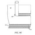
- FIG. 11Cis a plan view of a shutter having a recess accommodating a shaft.
- FIG. 12Aillustrates a plurality of heating elements arranged in concentric heating zones.
- FIG. 12Billustrates heating elements arranged concentrically relative to one another according to one embodiment of the present invention.
- FIGS. 12C and 12Dillustrates thermal isolation barriers arranged between heating zones according to one example of the present invention.
- FIG. 13illustrates a shaft conduit extending from a cooling chamber.
- FIG. 14illustrates the relative contributions of heat transfer from conduction and radiation.
- FIGS. 15A and 15Bare cross sectional views of a wafer holder according to one embodiment of the present invention.
- FIGS. 16A to 16 Dare cross sectional views of the wafer holder according to four alternative embodiments of the present invention.
- FIG. 17is an cross sectional view showing a portion of the wafer holder and wafer lift assembly in accordance with one embodiment of the present invention.
- FIG. 18is a perspective view showing the wafer holder in accordance with another embodiment of the present invention.
- FIG. 19is a cross sectional view showing the heat treating apparatus and wafer holder in accordance with one embodiment of the present invention.
- FIG. 20is an partial cross sectional view of the heat treatment apparatus showing the flow and containment of gases within the apparatus.
- FIG. 21is a cross sectional view of a heating zone for a preheat chamber in accordance with one embodiment of the present invention.
- FIG. 22is a perspective cross-sectional view of a portion of the heat treatment apparatus according to another embodiment of the present invention.
- FIG. 23is a cutaway perspective cross-sectional view of the shutter cavity portion of FIG. 22 .
- FIGS. 24A to 24 Care cross-sectional, top perspective and bottom perspective views, respectively, of another embodiment of the wafer carrier of the present invention.
- the present inventionrelates to a heat treatment apparatus.
- the heat treatment apparatusincludes a heating chamber with a heating source positioned adjacent to a cooling chamber with a cooling source.
- the apparatusalso includes a wafer holder configured to be moved between the heating chamber and the cooling chamber through a passageway.
- a shutteris positioned to control the size of the passageway. The shutter can be moved between an open position where the passageway is defined large enough for the wafer holder to pass through and a plurality of obstructing positions where a smaller passageway is defined. The shutter can be positioned in the obstructing positions whether the wafer holder is positioned within the cooling chamber or within the heating chamber.
- the shuttercan be constructed as a thermal insulator. Accordingly, when the shutter is positioned in an obstructing position, the shutter can serve to increase the thermal isolation between the heating chamber and the cooling chamber above the degree of thermal isolation which is achievable without the shutter.
- the increased thermal isolationalso allows for an increased difference between the average temperature within the heating chamber and the average temperature within the cooling chamber. For instance, for a given average temperature in the heating chamber, the cooling chamber can have a lower average temperature than would be possible without the shutter. Reducing the average temperature in the cooling chamber permits an increased temperature ramp down rate when the wafer is positioned within the cooling chamber. Similarly, increasing the average temperature in the heating chamber permits increased temperature ramp up rates when the wafer is within the heating chamber. Increasing the temperature ramp up and ramp down rates allows for quicker wafer treatment rates and accordingly quicker throughput.
- the heating sourcecan include a heating plate which receives heat rays from heating elements positioned above the heating plate.
- the heating platere-radiates the received heat into the heating chamber from a surface of the heating plate which is positioned within the heating chamber.
- the heating plateis constructed from a material with a high thermal conductivity so the received heat has a more uniform distribution across the heating plate. Increasing the uniformity of the thermal distribution within the heating plate also increases the uniformity of heat rays radiated into the heating chamber.
- the wafer holdercan be positioned anywhere within the heating chamber.
- the wafer holderis preferably positioned such that a wafer within the wafer holder is sufficiently close to the heating plate that heat is conducted from the heating plate to the wafer.
- the waferis preferably positioned within two millimeters of the heating plate. This positioning of the wafer relative to the heating plate allows the heat transfer to occur through both conduction and radiation. Since two forms of heat transfer deliver heat to the wafer, the apparatus can increase the temperature ramp up rate above the temperature ramp up rate achieved by apparatuses relying primarily on radiation as the heat transfer mechanism.
- the heating platecan define at least a portion of the upper end of the heating chamber and the path from the wafers to the heating plate can be unobstructed.
- This unobstructed pathpermits the wafer to be moved in closer proximity to the heating plate. Additionally, the unobstructed path prevents intervening mediums from altering the uniformity of the thermal distribution of heat produced by the heating plate. Further, the unobstructed path also permits more control over the conditions at the surface of the wafer. For instance, changes in the conditions of the heating plate, such as changes in the temperature of the heating plate, are transferred directly to the wafer without being delayed by transfer through some intervening medium.
- a relationship between the temperature of the heating plate and the temperature of the wafer surfacecan be developed for a particular displacement of the wafer from the heating plate. This relationship can be used to control the temperature of the wafer by adjusting the temperature of the heating plate. Since the heating plate has a large thermal mass, it acts as a thermal reservoir with a temperature which is easily monitored and controlled. Since the temperature of the heating plate is easily controlled, the above relationship allows the temperature of the wafer to be more easily controlled than is currently possible. Moreover, the present invention provides improved temperature stability and improved temperature control. For example, the present invention significantly reduces temperature overshoot problems and problems associated with thermal cycling. Also, there is a much lower peak power requirement, and better overall energy efficiency.
- a number of improved fluid delivery systemsare included in the scope of the present invention.
- a plurality of fluid portscan be formed in the upper end of the heating chamber.
- a fluidcan be delivered into the heating chamber through these fluid ports. Because these fluid ports are positioned at the upper end of the heating chamber, the fluid can be delivered onto an upper surface of a wafer in the wafer holder even when the wafer is positioned in close proximity to the upper end of the heating chamber.
- These fluid portscan be uniformly positioned across the upper end in order to increase the uniformity of the fluid delivery to the wafer.
- the increased uniformityallows for a plug type flow of liquid from the upper end of the heating chamber toward the wafer.
- a plug typeallows for a more rapid evacuation of fluid from the heating chamber.
- a plug type flowallows the fluids within the heating chamber to be rapidly exchanged with a reduced level of interaction between the exchanged gasses.
- the heating platecan be included in the upper end of the heating chamber, the fluid ports can be included in the heating plate. Accordingly, the heating plate can be used for delivery of both heat and fluids to the wafer; however this is just one example and other configurations can be used.
- the cooling source within the cooling chambercan include a cooling plate.
- the cooling platecan be positioned so that an upper surface of the cooling plate is adjacent to a wafer on the wafer holder when the wafer holder occupies one or more loading positions within the cooling chamber.
- the loading positionsare positions which the wafer holder can occupy while wafers are loaded and unloaded from the wafer holder.
- the cooling platepreferably has a high thermal conductivity so the cooling is distributed through an upper surface of the cooling plate and a high thermal emissivity so the cooling effects are distributed into the cooling chamber. Distribution of the cooling through the cooling plate increases the uniformity of cooling provided to the wafers and accordingly reduces the stress experienced by the wafers during cooling.
- the cooling sourcecan also include a cooling fluid conduit for delivering a cooling fluid into the cooling chamber.
- the cooling fluid conduitcan be used in conjunction with a cooling plate or can replace the cooling plate.
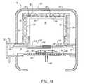
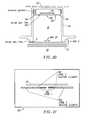
- FIG. 1Aillustrates a cross section of a heat treatment apparatus 10 .
- the apparatus 10includes a casing 12 which partially encloses a heating section 14 of the apparatus 10 .
- the heating section 14includes one or more thermal insulators 16 positioned adjacent to a heating chamber 18 .
- a plurality of heating elements 20are attached to a thermal insulator 16 adjacent to an upper end 22 of the heating chamber 18 .
- Suitable heating elements 20include, but are not limited to, resistive heating elements coupled with a power source controlled by a computer (not shown).
- the heating chamber 18is partially defined by a processing tube 24 .
- a heating plate 26defines the upper end 22 of the heating chamber 18 .
- the heating plate 26has a perimeter which is large enough to cover a wafer 28 positioned adjacent to the heating plate 26 .
- the heating plate 26can be constructed from the same materials as the rest of the processing tube 24 or can be constructed from different materials. Further, the heating plate 26 can be formed integrally with the remainder of the processing tube 24 or can be attached to the remainder of the processing tube 24 . Suitable materials for the processing tube 24 include, but are not limited to, high purity quartz, fused silica and silicon carbide. Further, the heating plate 26 is preferably constructed from materials with a high thermal conductivity such as silicon carbide and graphite covered with silicon carbide.
- the heating plate 26 and heating elements 20serve as an example of a heat source for use with the apparatus 10 .
- the heating plate 26receives heat rays radiated from the heating elements and radiates secondary heat rays into the heating chamber 18 .
- the heating plate 26can have a high thermal conductivity so the heat received from the heating elements 20 is distributed through the heating plate 26 .
- a plurality of secondary heating elements 30can optionally be coupled with the thermal insulators 16 adjacent to the sides of the processing unit.
- the secondary heating elements 30can provide additional heat to the heating chamber 18 and/or can be used to achieve better control over the temperature within the heating chamber 18 and to achieve better temperature uniformity.
- the heating elementsmay be of a resistive type.
- the apparatus 10also includes a cooling chamber 32 positioned adjacent the heating chamber 18 .
- FIG. 1Aillustrates a wafer 28 resting on a plurality of wafer support pins 34 extending upward from the bottom of the cooling chamber 32 .
- the cooling chamber 32can be accessed from a load/lock chamber through a slit valve 36 in order to load and/or unload a wafer 28 from the wafer support pins 34 .
- a robotic armcan be used to load and unload the wafer 28 from the pins.
- a single wafer 28is illustrated in FIG. 1A, a cartridge holding a plurality of wafers 28 can be supported on the wafer support pins 34 . Accordingly, the heat treatment apparatus 10 of the present invention can be used to concurrently treat a plurality of wafers 28 .
- FIG. 1Aalso illustrates a wafer holder 38 in a loading position beneath the wafer 28 .
- the loading positionsare positions occupied by the wafer holder 38 when a wafer 28 is loaded on and/or off the wafer support pins 34 .
- the wafer holder 38can have a ring shape, or a plate/disk shape, which encompasses the pins. As will be described in more detail below, the wafer holder 38 is configured to move between the cooling chamber 32 and the heating chamber 18 .
- a cooling source 40is positioned within the cooling chamber 32 so as to be beneath the wafer holder 38 when the wafer holder 38 is positioned within the cooling chamber 32 .
- the cooling source 40is preferably positioned adjacent to the bottom of the cooling chamber 32 and is most preferably positioned beneath the wafer 28 when the wafer holder 38 is in a loading position.
- the cooling source 40preferably includes a cooling plate 42 .
- the cooling plate 42can be positioned adjacent to one or more cooling fluid conduits 44 as illustrated in FIG. 1 A.
- a cooling plate 42can include one or more cooling fluid conduits 44 extending through the cooling plate 42 as illustrated in FIG. 1B.
- a cooling fluidcan be flowed through the cooling fluid conduits 44 .
- the cooling plate 42serves to distribute the cooling effect of these fluids across the surface of the plate so a wafer 28 being held by the wafer holder 38 sees a more uniform cooling effect.
- Suitable cooling fluids for use with the cooling fluid conduits 44include, but are not limited to, chilled water and liquid nitrogen.
- Suitable materials for the cooling plate 42include, but are not limited to, materials with a high thermal conductivity and/or a high thermal emissivity such as silicon carbide, aluminum, stainless steel, copper coated with silicon nitride and aluminum nitride.
- the cooling plate 42When the cooling source 40 is a cooling plate 42 , the cooling plate 42 preferably has a solid upper surface 46 which is substantially parallel to the plane of the wafer 28 in order to provide substantially uniform cooling to the wafer 28 .
- the cooling plate 42can include a plurality of apertures which are large enough to accommodate the wafer support pins 34 or the wafer support pins 34 can be mounted directly to the upper surface 46 of the cooling plate 42 .
- the upper surface 46 of the cooling plate 42preferably has a perimeter which is larger than the perimeter of the wafer 28 .
- the cooling plate 42is preferably positioned to be approximately concentric with wafers 28 positioned on the wafer support pins 34 or with wafers 28 being held by the wafer holder 38 .
- the cooling plate 42preferably has a round shape with a larger diameter than the wafer 28 .
- the round shape of the cooling plate 42is then positioned such that the center of the cooling plate 42 is positioned approximately beneath the center of the wafer 28 . This concentric positioning combined with the increased diameter of the cooling plate 42 relative to the wafer 28 causes the perimeter of the cooling plate 42 to extend beyond the perimeter of the wafer 28 .
- the wafer holder 38is coupled with a shaft 48 .
- the shaft 48can be coupled with an elevator mechanism (not shown) which can provide the shaft 48 with an upward and downward motion.
- the upward motion of the shaft 48elevates the wafer holder 38 as illustrated in FIG. 1 B.
- elevation of the wafer holder 38lifts the wafer 28 from the wafer support pins 34 and can move the wafer holder 38 from the cooling chamber 32 to the heating chamber 18 .
- the shaft 48can also be moved downward to move the wafer holder 38 from the heating chamber 18 to the cooling chamber 32 and to replace the wafer 28 upon the wafer support pins 34 .
- the wafer holder 38is illustrated as coupled with a single shaft 48 , the wafer holder 38 can be coupled with a plurality of shafts 48 including, but not limited to, two, three and four shafts 48 . Further, when the apparatus 10 includes a cooling plate 42 , the cooling plate 42 can include apertures configured to accommodate each of the shafts 48 coupled with the wafer holder 38 .
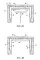
- the apparatus 10includes shutters 52 which define the size of a passageway 54 between the cooling chamber 32 and the heating chamber 18 .
- the shutters 52 illustrated in FIG. 1Bare positioned in an open position where the shutters 52 define a passageway 54 which is sufficiently large for the wafer holder 38 to pass between the heating chamber 18 and the cooling chamber 32 .
- the shutters 52can be coupled with motors 56 which serve to move the shutters 52 in a horizontal plane as illustrated by the arrow labeled B. Accordingly, the shutters 52 can be moved to an obstructing position where the shutters 52 define a passageway 54 which is smaller than the size of the passageway 54 defined when the shutters 52 are in the open position.
- FIG. 1Cillustrates the shutters in an obstructing position where the size of the passageway 54 approximates the size of the shaft 48 coupled with the wafer holder 38 . Accordingly, the shutter 52 can be in an obstructing position while the wafer holder 38 is positioned within the heating chamber 18 .
- the configuration illustrated in FIG. 1Cis the preferred configuration for the apparatus 10 during the treatment of the wafer 28 .
- Treatment of the wafer 28can include delivering a fluid, a gas or vapor to the wafer 28 in the heating chamber 18 .
- the obstructing position of the shutter 52 illustrated in FIG. 1Ccan also serve to reduce and even prevent entry of the fluids from the heating chamber 18 into the cooling chamber 32 . Accordingly, the shutters 52 can prevent these fluids from fouling mechanisms in the cooling chamber 32 or in an associated load/lock chamber.
- the shutter 52can also be constructed to act as a thermal insulator.
- the shutter 52serves to increase the thermal isolation of the heating chamber 18 and the cooling chamber 32 .
- the increased thermal isolationallows for an increased temperature difference between the average temperature in the heating chamber 18 and the average temperature in the cooling chamber 32 .
- the ratio of the average temperature in the heating chamber 18 to the average temperature in the cooling chamber 32can be higher than it could be without the shutter 52 .
- the wafer 28can be heated and/or cooled more quickly than would be possible without the shutter 52 .
- the increased thermal isolationalso reduces the amount of energy required to keep the average temperature in the heating chamber 18 and the cooling chamber 32 within a certain range.
- the shutter 52acts as a thermal insulator
- the shutter 52also serves to decrease the temperature drop between the shutter 52 and the heating plate 26 . Accordingly, the temperature adjacent the top of the shutter is closer to the hot plate temperature than could be achieved without the shutter 52 .
- the temperature in the heating chamber 18approaches isothermal which gives rise to improved uniformity of wafer temperature and run-to-run repeatability.
- the near isothermal nature of the heating chamber 18results in fewer cold spots being formed in the heating chamber 18 . The reduction in cold spots improves the thermal uniformity in the plane of the wafer 28 and between the top and bottom of the wafer 28 .
- FIGS. 1A-1Ceach illustrate the apparatus 10 including a shutter 52 , certain embodiments of the invention will not include a shutter 52 .
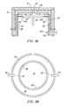
- FIG. 2Aillustrates another embodiment of the heat treatment apparatus 10 .
- the heating plate 26 and processing tube 24are independent of one another.
- the heating plate 26is positioned between the processing tube 24 and the heating elements 20 . Accordingly, the heating plate 26 serves to provide a more even thermal distribution than can be provided by the processing tube 24 alone.
- FIG. 2Billustrates another embodiment of an apparatus 10 where the heating plate 26 and the processing tube 24 are independent of one another.
- the heating plate 26is positioned inside the processing tube 24 so the heating plate 25 serves as the upper end 22 of the heating chamber 18 . Accordingly, heat from the heating elements 20 passes through the processing tube 24 before being distributed by the heating plate 26 .
- the heating plate 26can sit flush against the processing tube 24 or an air gap can be formed between the processing tube 24 and the heating plate 26 .
- Other embodiments of the apparatus 10do not include a heating plate 26 .
- the cooling sourcecan be eliminated from certain embodiments of apparatus 10 such as the embodiment of the apparatus 10 illustrated in FIG. 1 C.
- the cooling sourcecan include a plurality of cooling fluid conduits for delivery of a cooling fluid.
- the cooling fluid conduitscan be directed so as to be pointed toward the surface of wafer 28 within the cooling chamber 32 or can deliver the cooling fluid into the cooling chamber 32 at a location which is remote from the wafer 28 .
- the cooling fluid conduitcan be shaped as a loop with a perimeter exceeding the perimeter of the wafer holder 38 .
- the loop shaped cooling fluid conduitcan be positioned in the cooling chamber 32 so the wafer holder 38 can move through the cooling fluid conduit when the wafer holder 38 is carrying a wafer 28 .
- the loop shaped cooling fluid conduitcan have cooling fluid ports arranged around the perimeter of the loop. The cooling fluid can be delivered concurrently from a plurality of different cooling fluid ports to achieve a shower of cooling fluid onto a wafer 28 within the cooling chamber 32 . The shower effect produces a more uniform cooling to a wafer 28 than is achievable with discrete cooling fluid conduits, and allows forced convection cooling.
- FIG. 3illustrates a cooling fluid conduit used without a cooling plate 42
- one or more cooling fluid conduitscan be used in conjunction with a cooling plate to increase the temperature ramp down of a wafer 28 .
- treatment of a wafer 28 in the wafer holder 38can include delivery of a fluid to a surface of a wafer 28 in the heating chamber 18 .
- the following discussiondiscloses a variety of fluid delivery systems. Each of the apparatuses 10 illustrated above can be adapted for use with the fluid delivery systems described below. Additionally, the above discussion illustrates that the upper end 22 of the heating chamber 18 can be defined by a heating plate 26 or by the processing tube 24 . As a result, the upper end 22 of the heating chambers 18 illustrated below can be defined by a heating plate 26 or the processing tube 24 .
- FIG. 4Aprovides a bottom view of the upper end 22 of a heating chamber 18 .
- the upper end 22 of the heating chamber 18includes a plurality of fluid ports 70 . These fluid ports are formed in the heating plate 26 or in the processing tube 24 depending on whether the processing tube 24 or the heating plate 26 serves as the upper end 22 of the heating chamber 18 .
- the fluid ports 70are in fluid communication with one or more fluid sources. The fluid from these fluid sources can be delivered into the heating chamber 18 and/or the cooling chamber 32 through the fluid ports 70 . The position of the fluid ports 70 over the wafer 28 permits a downward flow of fluid from the fluid ports 70 onto the wafer 28 .
- An exhaust conduit(not illustrated) can be positioned in either the cooling chamber 32 or in the heating chamber 18 for removing the fluid delivered into the heating chamber 18 .
- a fluid exhaust conduitis preferably positioned near the bottom of the heating chamber 18 so as to be below the wafer 28 during the treatment of the wafer 28 . This position of the fluid exhaust port 93 relative to the wafer 28 during treatment of the wafer 28 causes the fluid delivered from the fluid ports 70 in the heating plate 26 to flow downward over the surface of the wafer 28 to the fluid exhaust port.
- the fluid ports 70can be evenly distributed across the upper end 22 of the heating chamber 18 as illustrated in FIG. 4 A.
- the fluid ports 70can be arranged in one of several different lattice patterns or in concentric geometric shapes. This even distribution of the fluid ports 70 encourages uniform fluid delivery across the plane of the wafer 28 and can encourage a plug type flow of the fluid from the upper end 22 of the heating chamber 18 toward the wafer 28 . This uniformity can be vital in processes such as chemical vapor deposition where a non-uniform distribution of fluids across the wafer 28 can result in uneven deposition results.
- the number of fluid ports 70 in the heating plate 26is preferably from 0 to 1000, more preferably from 200-800 and most preferably 550-650.
- the distance between adjacent fluid ports 70is preferably between 0.0 and 0.5 inches and is more preferably between 0.1 and 0.4 inches.
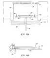
- FIG. 4Bprovides a cross section of the upper end 22 of a heating chamber 18 having a plurality of fluid ports 70 .
- the fluid ports 70are coupled with a conduit 80 formed in the heating plate 26 .
- the conduit 80terminates at a fixture 82 which is configured to be coupled with a fluid conduit.
- the fluid conduitcan be used to transport fluids into the heating chamber 18 through the fluid ports 70 and/or can be used to withdraw fluid from the heating chamber 18 through the fluid ports 70 .
- FIG. 4Cillustrates another example of the upper end 22 of a heating chamber 18 .
- the fluid ports 70extend through the portion of the processing tube 24 defining the upper end 22 of the heating chamber 18 .
- An external lumen 84is coupled to the top of the upper end 22 of the heating chamber 18 such that the lumen is in fluid communication with each fluid port 70 .
- the fluid portscan be divided into a first group of fluid ports 70 and a second group of fluid ports.
- the first group of fluid ports 70can be in fluid communication with a first fluid conduit and the second group of fluid ports 70 can be in fluid communication with a second fluid conduit which is independent of the first fluid conduit.
- Different fluidscan be delivered through the first fluid conduit and the second fluid conduit.
- a different fluidcan be delivered from the first group of fluid ports 70 than is delivered from the second group of fluid ports 70 .
- the first fluid conduitcan be used to deliver fluid into the heating chamber 18 while the second fluid conduit is used to withdraw fluid from the heating chamber 18 .
- FIG. 5Aillustrates a fluid delivery system where the heat treatment apparatus 10 includes a fluid inlet conduit 88 terminating in a fluid inlet port 90 and a fluid exhaust conduit 92 terminating in a fluid exhaust port 93 .
- the fluid inlet port 90 and the fluid exhaust port 93can be positioned anywhere within the heating chamber 18 .
- the fluid inlet port 90 and the fluid exhaust port 93are preferably at a height which allows them to be above the surface of the wafer 28 during treatment of the wafer 28 .
- This position of the fluid inlet port and the fluid exhaust portpermits the fluid to be flowed from the fluid inlet port 90 to the fluid exhaust port 93 across the surface of the wafer 28 . Accordingly, a fluid flow region is defined between the wafer and the upper end of the heating chamber during treatment of the wafer.
- a fluid inlet port 90can be positioned above the wafer 28 during treatment of the wafer 28 and a fluid exhaust port 93 can be positioned below the wafer 28 in the heating chamber 18 or within the cooling chamber 32 . This position of the fluid inlet port 90 relative to the fluid exhaust port 93 creates a downward fluid flow in the heating chamber 18 .
- the fluid conduitscan be operated in reverse so the fluid exhaust port 93 is above the wafer 28 during treatment of the wafer 28 and the fluid inlet port 90 is below the wafer 28 during treatment of the wafer 28 .
- FIG. 6Aillustrates a heating chamber 18 which includes a flow containment member 94 extending inward from the side of the processing tube 24 .
- a wafer 28can be positioned in the heating chamber 18 so the wafer 28 and the flow containment member 94 define a lower side of a fluid flow region 96 within the heating chamber 18 .
- Suitable materials for the flow containment member 94include, but are not limited to, high purity quartz, fused silica and silicon carbide.
- the flow containment member 94can be integral with the processing tube 24 or can be an independent piece attached to the processing tube 24 with techniques such as welding.
- FIG. 6Bis a cross sectional view of processing tube 24 looking downward into the heating chamber 18 at the axes labeled A in FIG. 6 A.
- An inner edge 98 of the flow containment member 94has a shape complementary to the shape of a portion of the wafer perimeter. Additionally, the inner edge 98 of the flow containment member 94 is larger than the portion of the wafer perimeter to which the inner edge is complementary. The difference in the perimeter size of the wafer 28 and the perimeter size of the inner edge 98 of the fluid containment plate allows a wafer 28 to be positioned adjacent to the flow containment member 94 with a gap 100 formed between the wafer 28 and the inner edge 98 of the flow containment member 94 .
- This gap 100provides a route where fluids delivered into the fluid flow region 96 can escape the fluid flow region 96 .
- An auxiliary fluid exhaust conduit 102 with an auxiliary fluid exhaust port 104can optionally be positioned below the flow containment member 94 in order to evacuate fluids which escape from the fluid flow region 96 from the heating chamber 18 .
- the flow containment member 94is sized to provide a gap 100 which reduces escape of the fluids from the fluid flow region 96 into the remaining portions of the heating chamber 18 .
- the wafer 28is preferably positioned adjacent to the flow containment member 94 .
- the fluid flow region 96limits the volume of atmosphere within the heating chamber 18 which must be controlled during the treatment of the wafer 28 . Since atmospheric conditions are easier to control in a small volume than in a larger volume, the atmospheric conditions are easier to control in the fluid flow region 96 than would be possible to achieve in the entire heating chamber 18 . For instance, uniformity of temperature is easier to control in a small volume than in a large volume. Accordingly, the fluid flow region 96 allows for a more easily controlled temperature.
- the fluid flow region 96can simplify the process of changing gasses within the heating chamber 18 while reducing interaction between the gasses.
- the fluid flow region 96preferably has a substantially constant distance between the bottom side of the fluid flow region 96 and the upper end 22 of the heating chamber 18 .
- the constant distanceencourages a plug flow pattern for the fluid flowing from the fluid inlet conduit to the fluid exhaust conduit.
- a plug flow patternallows one gas to follow another gas with only minimal interaction of the two gasses.
- fluids within the fluid flow region 96can be changed by flowing a fluid through the fluid flow region 96 , terminating the flow of that fluid and concurrently starting the flow of another fluid through the fluid flow region 96 .
- FIGS. 6A-6Billustrate a single fluid exhaust conduit 92 having a single fluid exhaust port 93 and/or a single fluid inlet conduit 88 with a single fluid inlet port 90
- the apparatus 10can include a plurality of fluid inlet conduits 88 and/or a plurality of fluid exhaust conduits 92 .
- a single fluid inlet conduit 88can have a plurality of fluid inlet ports 90 .
- the apparatus 10can include a plurality of fluid exhaust conduits 92 and a single fluid exhaust conduit 92 can include a plurality of fluid exhaust ports 93 . Increasing the number of fluid conduits and the number of fluid ports in an apparatus 10 permits a greater degree of control over the conditions of the fluid at the surface of the wafer 28 .
- FIG. 6Cis a cross sectional view of a rectangular shaped processing tube 24 looking downward into the heating chamber 18 at the axis labeled A in FIG. 6 A.
- the apparatus 10includes a plurality of fluid inlet ports positioned above a flow containment member 94 . Each fluid inlet port is aligned with a fluid exhaust port on an opposite side of the fluid flow region 96 .
- the plurality of fluid inlet ports and fluid exhaust portscan increase the plug flow characteristic of the fluid flow across the surface of the wafer 28 .
- FIG. 6Dillustrates an apparatus 10 having a plurality of flow containment members 94 arranged on opposing sides of the heating chamber 18 .
- the inner edge 98 of each flow containment member 94has a shape complementary to the shape of a portion of the wafer perimeter. Additionally, the inner edge 98 of each flow containment member 94 is larger than the portion of the wafer perimeter to which the shape is complementary. As a result, each flow containment member 94 can be positioned adjacent a portion of a wafer 28 with a gap 100 formed between the wafer 28 and the inner edge 98 of the flow containment member 94 .
- FIG. 7Aillustrates a flow distribution member 106 positioned between the flow containment member 94 and the wall of the processing tube 24 .
- the flow distribution member 106is particularly suited for oxidation and atmospheric pressure processing.
- a flow distribution member 106is associated with the fluid inlet conduit and a flow distribution member 106 is associated with the fluid exhaust conduit.
- the flow distribution member 106can be positioned at the inner edge 98 of the flow containment plate or can be closer to the wall of the processing tube 24 .
- FIG. 7Bis a side view of a flow distribution member 106 .
- a plurality of holes 108are formed through the flow distribution member 106 .
- the holes 108preferably have a diameter between 0.01-0.1 inches, more preferably between 0.15-0.02 inches and most preferably between 0.02-0.03 inches.
- the holes 108are preferably spaced to achieve a plug type flow from the flow distribution member.
- the holes 108can have different sizes to encourage a more even flow.
- the holes 108 directly in front of the fluid inlet portcan have a smaller diameter than the holes 108 at the periphery of the fluid inlet port. The smaller diameter encourages a flow of fluid to the holes 108 at the periphery.
- Other embodiments of flow distribution members 106include, but are not limited to, mesh screens and wire grids.
- the number, size and arrangement of the holes 108 in a flow distribution member 106 associated with a fluid inlet conduitcan be the same as or different from the number of holes 108 in a flow distribution member 106 associated with a fluid exhaust conduit.
- the wall of the processing tube 24 and the flow distribution member 106act together to form a fluid flow distribution chamber 110 around a fluid inlet port.
- the flow distribution chamber 110increases the area from which fluid enters the fluid flow region 96 over the area which would be possible without the flow distribution chamber 110 .
- a flow distribution chamber 110can also be formed around a fluid exhaust port.
- a flow distribution chamber 110 around a fluid exhaust portcan serve to spread out the flow of fluid leaving the fluid flow region 96 . As a result, this flow distribution chamber can prevent the fluid within the fluid flow region 96 from converging at the fluid exhaust port.
- the effect of the flow distribution chambers 110 formed around the fluid inlet port and the fluid chamber formed around the fluid exhaust portis to increase the plug flow characteristics of the fluid flow across the surface of the wafer 28 .
- a flow distribution chamber 110can also be constructed in different ways.
- the flow distribution chamber 110can be filled with a porous media or diffusing material such as metal chips.
- FIG. 7Cis a cross sectional view of a processing tube 24 having a rounded cross section.
- the flow distribution chamber 110 around the fluid inlet port and the flow distribution chamber 110 around the fluid exhaust porthave arc shapes. Although the flow distribution chambers 110 are illustrated as arcing over a 180° range, flow distribution chambers 110 arcing over smaller angular ranges are also contemplated.
- FIG. 7Dillustrates a processing tube 24 with a rounded cross section and flow distribution members 106 with a straight contour.
- This geometryhas the advantage that the flow distribution chambers 110 are equidistant along their length. As a result, the distance a fluid travels between the flow distribution chambers 110 is more uniform than is possible when the flow distribution member 106 has a curved contour.
- the increased uniformitycan increase the similarity between the fluid flow conditions experienced by the center of the wafer 28 and the conditions experienced at the edge of the wafer 28 midway between the two flow distribution chambers 110 .
- FIG. 7Eis a cross sectional view of a processing tube 24 having a rectangular cross section.
- the flow distribution members 106both have a straight contour. This geometry has the advantages associated with flow distribution chambers 110 which are equidistant along their length.
- FIGS. 7A-7Eeach illustrate a single fluid inlet port and a single fluid exhaust port associated with each flow distribution chamber 110
- each flow distribution chamber 110can be associated with a plurality of fluid inlet ports and/or a plurality of fluid exhaust ports.
- the flow distribution chamber 110can be partially defined by a second flow containment member 94 extending inward from the side of the processing tube 24 .
- the flow distribution member 106is positioned between the flow containment member 94 and the second flow containment member 94 .
- the second flow containment member 94can optionally include a recess sized to receive the edge of a heating plate 26 .
- the second flow containment member 94can support the heating plate 26 .
- the heating plate 26can sit flush against the processing tube 24 or an air gap can be formed between the processing tube 24 and the heating plate 26 .
- a single heating chamber 18can include several flow distribution chambers 110 positioned at different heights. As a result, a wafer 28 can be treated at different distances from the upper end of the heating chamber 18 .
- FIG. 9Aprovides a cross section of a heat treatment apparatus 10 having an enlarged fluid inlet port and an enlarged fluid exhaust port.
- the waferis preferably positioned adjacent the lowest point of the fluid inlet port.
- a portion of the fluid inlet conduit, the fluid flow region and a portion of the fluid exhaust conduitcombine to form a fluid flow passage 112 with a substantially constant cross sectional geometry extending through the portion of the fluid inlet conduit, the fluid flow region and the portion of the fluid exhaust conduit.
- the substantially constant cross sectional geometrymeans the fluid flow pattern in one portion of the flow passage 112 is substantially retained through the flow passage 112 . This allows the flow pattern in the fluid inlet port to be retained across the fluid flow region. As a result, when a plug type flow is created in the fluid inlet port, the plug type flow is substantially retained through the fluid flow region.
- FIG. 9Bis a cross section of the processing tube 24 looking down into the tube at the axis marked A
- FIG. 9Cis a cross section of the processing tube 24 looking up into the processing tube 24 at the axis marked B.
- the fluid flow region 96is partially defined by flow region defining walls 114 positioned on opposing sides of the flow region.
- the flow region defining walls 114can have a variety of positions relative to the fluid inlet conduit and the fluid exhaust conduit.
- FIG. 9Dis a cross section of a processing tube 24 where the flow region defining walls 114 are sized to separate the fluid inlet conduit from the fluid exhaust conduit.
- a flow distribution member 106is positioned within the fluid inlet conduit. Similarly, a flow distribution member 106 is positioned within the fluid exhaust conduit. As a result, a flow distribution chamber 110 is formed within the fluid inlet conduit and within the fluid exhaust conduit.
- the flow distribution members 106can be positioned at the fluid inlet port or along the length of the fluid exhaust conduit. The flow distribution members 106 serve to spread the fluid flow out over the width of the fluid inlet conduit and/or the fluid exhaust conduit. As a result, the flow distribution members 106 encourage a plug type flow in the fluid flow passage 112 .
- the fluid inlet conduit and the fluid exhaust conduithave a shape matched to the shape of the fluid flow region 96 .
- the fluid flow region 96has width about the width of the wafer 28 .
- the fluid inlet conduit and the fluid exhaust conduithave widths, W, on the order of the wafer diameter.
- the fluid flow region 96has a thickness about the thickness of the fluid inlet port.
- the fluid inlet conduit and the fluid exhaust conduithave a thickness, T, which approximates the thickness of the fluid inlet port.
- the constant shapes of the fluid inlet conduit, the fluid flow region 96 and the fluid exhaust conduitallows the fluid to retain a similar flow pattern in each of the fluid inlet conduit, the fluid flow region 96 and the fluid exhaust conduit.
- the fluid flow pattern at the wafer surfacecan be controlled by controlling the fluid flow pattern in the fluid inlet conduit.
- a fluid inlet conduit and a fluid exhaust conduitcan have shapes matched to the fluid flow region 96 and can be independent of the processing tube 24 .
- a single processing tube 24can include a combination of the above fluid delivery systems.
- a single apparatus 10can include fluid ports 70 arranged in a heating plate 26 , a fluid inlet conduit 88 and a fluid exhaust conduit 92 positioned on opposing sides of a fluid flow region 96 .
- FIG. 10Aprovides a side view of shutters 52 designed to provide thermal insulation.
- the shutter 52is constructed from a plurality of members 116 . Suitable materials for constructing these members 116 include, but are not limited to, quartz covered insulators, silicon carbide, opaque quartz and fused silica.
- the members 116are arranged. to at least partially define open air gaps 118 between adjacent members 116 . Because air has a low thermal conductivity, these open air gaps 118 add thermally insulative properties to the shutter 52 .
- the open air gaps 118have a height which is preferably slightly larger than the thickness of each member 116 .
- the open nature of the air gaps 118allows the shutters 52 to be meshed together as illustrated in FIG. 10 B. Specifically, a portion of one shutter 52 is slidably received within a portion of another shutter 52 . When one shutter 52 is slidably received in another shutter 52 , the members of the opposing shutters 52 preferably do not touch one another in order to avoid the production of particulates in the heating chamber 18 .
- FIG. 11Aprovides a top view of the shutters 52 when they are positioned in the obstructing position illustrated in FIG. 1 C.
- the shutters 52include recesses 120 which have a geometry matched to the size and shape of the shaft 48 coupled with the wafer holder 38 . Accordingly, when the wafer holder 38 is positioned in the heating chamber 18 the shutters 52 can be moved together so they form a passageway 54 with a shape approximating the shape of the shaft 48 . Because the passageway 54 has a shape which is complementary to the shaft 48 , the shaft 48 fits snugly within the passageway 54 to reduce exchange of gasses between the heating chamber 18 and the cooling chamber 32 and to reduce radiative heat transfer from the heating chamber 18 to the cooling chamber 32 . This shape can also serve to reduce radiative heat transfer from the heating chamber 18 to the cooling chamber 32 .
- FIG. 11Bprovides a top view of the shutters 52 when they occupy an obstructing position such as the position of the shutters 52 illustrated in FIG. 1 A.
- the shutters 52are slid far enough together to effectively close the passageway 54 .
- the passageway 54can be closed to increase the thermal isolation of the cooling chamber 32 and the heating chamber 18 . Accordingly, the shutter configuration of FIG. 11B is desirable when the wafer holder 38 is positioned in the cooling chamber 32 .
- FIG. 11Cillustrates a single shutter 52 which can be used to define the size of the opening.
- the single shutter 52includes a deep recess 120 which receives the shutter 52 when the shutter 52 is positioned in an obstructing position and the wafer holder 38 is positioned within the heating chamber 18 .
- the recess 120is preferably deep enough that the shutter 52 can extend across the passageway 54 between the cooling chamber 32 and the heating chamber 18 when the wafer holder 38 is positioned within the heating chamber 18 .
- the shutters 52 illustrated in FIGS. 11A-11Cinclude a single recess 120 for accommodating a shaft 48 coupled with the wafer holder 38 ; however, the shutters 52 can include a plurality of recesses 120 for accommodating a plurality of shafts 48 coupled with a wafer holder 38 .
- each shutter 52 illustrated aboveare constructed from a plurality of members 116 , each shutter 52 can be constructed fro a single member 116 . Additionally, each passageway 54 illustrated above is constructed from two shutters 52 ; however, the apparatus 10 can include three or more shutters 52 which define a single passageway 54 . In another embodiment, seven shutters 52 are used which move into one recess.
- FIGS. 12A-12Dillustrate possible arrangements for the heating elements 20 used with the apparatuses 10 disclosed above.
- the heating elements 20are each arranged in concentric heating zones 122 .
- the heating elements 20 in a particular heating zone 122can be arranged in concentric circles as illustrated in FIG. 12 A.
- a single heating element 20 with a rounded geometrycan occupy a heating zone 122 as illustrated in FIG. 12 B.
- the heating elements 20 in different heating zones 122are preferably controlled independently.
- the heating elements 20can be eclectically connected in series or in parallel or can be independently controlled.
- Thermocouplesmay be placed in the center of each zone to provide temperature feedback.
- Thermal isolation barriers 124can be positioned between the heating zones 122 as illustrated in FIG. 12 C. As illustrated in FIG. 12D, the thermal isolation barriers 124 can extend from the thermal insulator 16 toward the processing tube 24 and can be coupled to the processing tube 24 . In another embodiment, the thermal isolation barriers 124 extend from the insulation toward a heating plate 26 and can be coupled to the heating plate 26 .
- the thermal isolation barriers 124can reduce the cross talk of the heat produced by the heating elements 20 in different heating zones 122 . As a result, the heat produced in a particular heating zone 122 is directed toward the heating plate 26 or the processing tube 24 . Accordingly, adjustments made to a particular heating element 20 affect primarily the portion of the heating plate 26 or the processing tube 24 which are adjacent the adjusted heating element 20 . As a result, the thermal isolation barriers 124 serve to increase the degree of control over the thermal conditions within the heating chamber 18 .
- FIGS. 12A-12Dillustrate a processing tube 24 having a rounded cross section
- the heating elements 20 and thermal isolation barriers 124can be adapted to processing tubes 24 having a rectangular cross section.
- FIG. 13illustrates an apparatus 10 having a shaft conduit 126 extending from the cooling chamber 32 .
- the shaft conduit 126encloses a portion of the shaft 48 extending below the cooling chamber 32 .
- the shaft conduit 126can be integral with the frame of the cooling chamber 32 or can be an independent piece which is attached to the frame of the cooling chamber 32 .
- the shaft conduit 126can be a bellows (not shown), having an “accordion” shape. Any of the apparatuses 10 disclosed above can be adapted for use with the shaft conduit 126 .
- a seal 128is formed between the shaft conduit 126 and the shaft 48 at a position which is remote from the cooling chamber 32 .
- the seal 128serves to reduce the escape of fluids from the cooling chamber 32 and/or to reduce the entry of fluids from the atmosphere into the cooling chamber 32 .
- the seal 128helps to increase the thermal and physical isolation of the cooling chamber 32 from the atmosphere. This isolation enhances the controllability of the atmosphere within the cooling chamber 32 .
- the remote location of the seal 128reduces the heat to which the seal 128 is exposed. For instance, while the wafer 28 is positioned within the heating chamber 18 , the portion of the shaft 48 within the heating chamber 18 heats up. However, lower portions of the shaft 48 retain cooler temperatures because they are nearer the cooling chamber 32 and/or because they spend less time in the heating chamber 18 .
- the position of the seal 128 remote from the cooling chamber 32results in exposure of the seal 128 to lower portions of the shaft 48 than would occur if the seal 128 were within or adjacent to the cooling chamber 32 . As a result, the position of the seal 128 remote from the cooling chamber 32 can serve to protect the seal 128 from heat damage and can accordingly preserve the seal 128 .
- the distance of the seal 128 away from the cooling chamber 32is preferably equal to about the maximum distance which the shaft 48 extends into the heating chamber 18 .
- a seal 128can be formed at the junction of the cooling chamber 32 and the shaft 48 . Such a seal 128 is an alternative to, or can be used in conjunction with, the seal 128 between the shaft 48 and the shaft conduit 126 .
- the inventionalso relates to a method of operating the apparatus 10 .
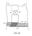
- the wafer holder 38can be positioned anywhere within the heating chamber 18 during the ramp up of the wafer 28 temperature.
- the wafer 28is preferably positioned so close to the heating plate 26 that the heat is conducted to the wafer 28 through the air between the heating plate 26 and the wafer 28 .
- the close proximity of the wafer 28 and the heating plate 26causes the wafer 28 to be concurrently heated by both radiation and conduction.
- These two heat transfer mechanismsprovide an accelerated temperature ramp up.
- the inventionis not limited however, and the heat treatment apparatus may be operated in a non-conductive mode where the wafer is away from the hot plate.
- the percentage of heat transferred to the wafer 28 by conductionis preferably 20-90%, more preferably between 20-70%.
- the wafer 28is preferably positioned within 2 mm of the heating plate 26 and more preferably within 1 mm of the heating plate 26 .
- the distance between the wafer 28 and the heating plate 26 which is required to achieve a particular degree of heat transferred by conductionis a function of the temperature at the heating plate 26 . For instance, when the temperature of the heating plate 26 is approximately 900° C., the wafer 28 is preferably positioned within 2 mm of the heating plate 26 .
- the wafer 28is preferably positioned within 0.8 mm of the heating plate 26 .
- the distance between the wafer 28 and the heating plate 26can be varied during treatment of the wafer in order to control the heating rate. For instance, the ramp up rate can be increased by moving the wafer closer to the heating plate 26 .
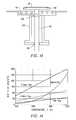
- FIG. 14illustrates the heat flux due to radiation compared with the heat flux due to conduction at two different displacements of the wafer from the heating plate 26 .
- Heat transferoccurs mainly by radiation, however; as illustrated, the percentage of heat flux from conduction increases with proximity of the wafer to the heating plate 26 .
- the heat flux due to conductionis about two thirds of the total heat flux.
- the heat flux due to conductionis reduced to about one third of the total heat flux.
- a wafermust be placed in close proximity to the heating plate 26 in order to obtain the benefits of conductive heat flux.
- the wafer 28can be treated. For instance, once the wafer 28 reaches a target temperature, a fluid can be delivered into the heating chamber 18 . Alternatively, once the target condition has been achieved at the wafer 28 , the wafer 28 can be backed away from the heating plate 26 . Backing the wafer 28 away from the heating plate 26 can serve to move the wafer 28 under a fluid inlet port 90 coupled with a fluid inlet conduit 88 or can provide improved flow characteristics of a fluid over the wafer 28 by increasing the clearance between the wafer 28 and the heating plate 26 .
- the wafer 28can be rotated by rotating the wafer holder 38 .
- the wafer 28is preferably rotated at 0 to 600 r.p.m. and more preferably at 5 to 15 r.p.m.
- the rotation of the wafer 28can serve to provide a more uniform exposure of the wafer 28 to fluids delivered into the heating chamber 18 during the treatment of the wafer 28 .
- the rotation of the wafer 28can also provide a more uniform thermal budget.
- the shutters 52can be opened and the wafer holder 38 can be lowered into the cooling chamber 32 .
- a target conditioncan then be achieved at the wafer 28 before the wafer 28 is removed from the wafer holder 38 .
- the wafer 28can be reduced to within a range of target temperatures before the wafer 28 is removed from the wafer holder 38 .
- a wafer holder and heat treatment apparatusconfigured to promote more uniform heating of the wafer supported by the wafer holder. More specifically, a wafer holder and heat treatment apparatus is provided which minimizes thermal stresses in the wafer during heating and cooling in the heat treatment apparatus. During heating of the wafer in the heating chamber the peripheral edge of the wafer will heat up more rapidly than the center of the wafer. Similarly, during cooling the peripheral edge of the wafer will cool down more rapidly than the center of the wafer. These differences in temperature between the edge and the center of the wafer create thermal stresses within the wafer. Such thermal stresses are problematic, particularly at high temperatures, and can lead to failure of the semiconductor devices formed on the wafer.
- the wafer holder and apparatus of the present inventionis configured to slow down the thermal ramp rate of the peripheral edge of the wafer. This is accomplished by employing a wafer holder having an edge effect member located proximate to at least a portion of the peripheral edge of the wafer.
- a wafer holder having an edge effect member in accordance with the present inventionis illustrated in FIG. 15 .
- the wafer holder 138generally includes one or more wafer support members 140 and an edge effect member 142 .
- the one or more wafer support members 140retain the wafer 28 in the wafer holder 138 and support the wafer in a substantially planar manner.
- the wafer support members 140may be any suitable support members and are not limited to any particular design.
- suitable support members 140include, but are not limited to, a plurality of upwardly extending pins, a flat base plate, a recessed base plate, an annular ring, a guard ring, and the like.
- the wafer support members 140will provide for secure support and retention of the wafer during rotation of the wafer support.
- the wafer holder 138is coupled to the shaft 48 which raises and lowers the wafer holder within the heat treatment apparatus. 10 .
- the wafer holder 138includes an edge effect member 142 .
- the edge effect member 142acts to minimize the temperature differential that occur between the wafer edge, and the center of the wafer, during heating and cooling of the wafer in the heat treatment apparatus.
- the wafer holder 138 having an edge effect member 142according to one embodiment is shown.
- the wafer holder 138includes a support member 140 comprised of a flat base plate 141 that extends the entire diameter of the wafer, and an upwardly extending edge effect member 142 positioned near the outer edges of the base plate 141 .
- the edge effect member 142is spaced apart from the peripheral edge of the wafer 28 .
- the edge effect member 142is comprised of a vertically oriented (i.e. normal to the wafer) circular band, that extends upwardly from the base plate 141 and encircles or rings at least a portion of the peripheral edge of the wafer 28 .
- the edge effect member 142encircles the substantial peripheral edge of the wafer, and most preferably the edge effect member 142 encircles the entire periphery of the wafer.
- the edge effect member 142may be formed integral with the base plate 141 or can be an independent piece that is attached to the base plate 141 via known techniques such as welding.
- the edge effect member 142extends above the position of the wafer, thereby creating a thermal barrier around the periphery of the wafer.
- the edge effect member 142also blocks any radiation emanating from the side walls of the heating chamber.
- the edge effect member 142provides a thermal mass located near the peripheral edge of the wafer. This thermal mass will draw heat away from the edge of the wafer during heating if the temperature of the thermal mass lags behind the temperature of the wafer during heating. To promote this behavior, the wafer holder with edge effect member is designed to have a thermal mass to energy absorption ratio larger than that of the wafer (or other substrate material). The wafer holder and its edge effect members will have a thickness, specifically t 1 , and t 2 as illustrated in FIG. 15 . Wafer holder materials which will provide a suitable thermal mass include but are not limited to, quartz, silicon carbide, A1 2 O 3 , fused silica, silicon, or ceramic.
- the wafer holder and the edge effect memberare typically formed of the same material. However they can be formed of different materials. Thickness values (t 1 , and/or t 2 ) of the wafer holder that will provide a suitable thermal mass are in the range of about 0 to 10 mm, more preferably in the range of about 0.5 to 4 mm, with a range of about 0.75 to 2 mm being most preferred. It will be apparent to those of ordinary skill in the art, that the above described parameters, such as the design conditions of volume and thickness and the material characteristics of density, specific heat, emissivity and reflectivity can be selected to produce the desired thermal mass to energy absorption ratio and thus the desired temperature profile across the wafer can be tailored.
- the desired objectiveis typically to minimize the temperature deviation within the wafer (i.e. between the edges and the center), and thus the edge effect member is employed to promote substantially uniform heating and cooling across the wafer.
- the edge effect member according to the present inventionis comprised of an opaque or partially opaque material. This provides the additional advantage of selectively blocking radiative heat transfer from the heating source to the edges of the wafer.
- the edge effect membermay be placed in a variety of orientations relative to the wafer to tailor the blocking of the radiative heat transfer. For example, as described in more detail below, the edge effect member may be placed above the peripheral edge of the wafer thereby blocking radiation from the edge of the wafer that emanates from the heating source in the upper end of the heating chamber.
- Preferred materials that provide an opaque or partially opaque materialinclude, but are not limited to, quartz, silicon, silicon carbide, or fused silica
- the edge effect memberis spaced apart from the peripheral edge of the wafer by a distance d, as illustrated in FIGS. 15 and 16A to 16 D.
- the edge effect membershould be placed at a distance “d” of up to approximately one inch from the peripheral edge of the wafer 28 .
- the edge effect memberis placed at a distance d of approximately 0.5 to 10 mm from the peripheral edge of the wafer 28 .
- FIG. 15While one embodiment of the edge effect member 142 is illustrated in FIG. 15, the configuration of the edge effect member 142 may take a variety of forms. Alternative embodiments are shown in FIGS. 16A to 16 B.
- FIG. 16Aa wafer holder with a similar configuration as that shown in FIG. 15 is illustrated with a vertically orientated edge effect member encircling the peripheral edge of the wafer; except in this embodiment, the support member 140 is comprised of two outwardly extending, opposed plates 144 and 145 which support the wafer along its edges as opposed to the flat base plate 141 that extends the entire diameter of the wafer.
- the support member 140is comprised of a circular support disk or ring 143 (FIG. 17) which supports the wafer along its periphery.
- the wafer holder 138is comprised of a support member 146 and an edge effect member 148 .
- the edge effect member 148is spaced apart from the peripheral edge of the wafer 28 and is comprised of a horizontally oriented (i.e. parallel to the wafer) circular band that encircles at least a portion or the peripheral edge of the wafer.
- the edge effect member 148encircles the substantial peripheral edge of the wafer 28 , and most preferably it encircles the entire periphery of the wafer.
- the edge effect member 148may be placed either underneath the peripheral edge of the wafer as illustrated in FIG.
- the wafer holderprovides the added effect of preventing radiative heat transfer to the edge of the wafer from the heating source in the upper end of the heating chamber. This, in addition to the thermal affect of the edge effect member, helps to slow the heat up of the edge of the wafer and thus brings the ramp rate of the edge of the wafer closer to that of the center of the wafer, thereby reducing the temperature non-uniformity within the wafer 28 .
- the edge effect member 148when the edge effect member 148 is positioned parallel to the wafer, either above or below the wafer, the edge effect member 148 should extend over the wafer edge.
- the edge effect member 148will extend over (or under, as the case may be) the edge of the wafer by approximately 0-10 mm.
- the support member 140may be comprised of any suitable support.
- the support member 140is comprised of a plurality of straight pins 150 which are carried by and extend upward from the horizontal edge effect member 148 to engage the underside of the wafer 28 .
- the pinscould be carried by another member extending from the chamber walls as opposed to being carried by the edge effect member.
- a retaining ringmay also be used.
- the support member 140is comprised of an L-shaped member 152 carried by the edge effect 148 which hangs from the edge effect member and has an outwardly projecting portion 153 which projects under the wafer.
- the outwardly projecting portion 153includes a plurality of pins 154 to engage the underside of the wafer 28 .
- the support member 140may take a variety of configurations, and is not limited to the exact embodiments shown here. The only limitation is that the support member provide secure support of the wafer.
- the edge effect member 148is comprised on two portions, an upper 156 a and lower 156 b portion, and resembles an upside-down L shaped band that encircles at least a portion of the wafer.
- the upper portion 156 ais parallel to the horizontal plane of the wafer, and is positioned spaced apart and above the wafer.
- the upper portion 156 aextends over the wafer edge and thus provides the additional affect of blocking at least a portion of the radiative heat transfer from the heat source in the upper end of the chamber to the wafer edge. Coupled to the upper portion 156 a is the lower portion 156 b .
- the lower portion 156 bis vertically oriented, normal to the horizontal plane of the wafer, and is positioned spaced apart from the wafer.
- the upper and lower portionsmay be formed in one integral piece, or alternatively the two portions may be formed of separate pieces and then attached to each other via known techniques such as welding.
- this embodiment of the wafer holderprovides the dual effect of (1) slowing the heating and cooling non uniformities in the edge of the wafer by the thermal mass positioned near the edge of the wafer, and (2) blocking at least a portion of the radiative heat transfer from the upper end of the chamber to the edge of the wafer.
- the wafer holderincludes a wafer lift assembly 170 .
- the wafer lift assembly 170generally includes a plurality of lifter pins 172 coupled via an elevator rod 174 .
- the elevator rodcontains three spokes connected to three lifter pins 172 .
- the lifter pinsextend and retract through openings in the support member 140 to raise and lower the wafer 28 .
- the lifter pinsare extended, and the wafer 28 , carried typically by and end effector (not shown) is positioned above the pins and then placed on the extended pins. In the extended position, the pins extend a distance above the height of the edge effect member.
- the lifter pinsretract through the openings in the support member 140 thereby bringing the wafer to rest on the support member as illustrated in FIG. 17 . After processing, the lifter pins again extend and lift the wafer above the edge effect member and the wafer is removed.
- FIG. 19shows one embodiment of the wafer holder positioned within the heat treatment apparatus according to one embodiment of the present invention.
- the wafer holder 138includes the wafer support member 140 and the edge effect member 142 .
- the edge effect member 142is adjacent and spaced apart from the flow containment member 94 , with a gap formed between the outer diameter of the wafer holder 138 and the inner diameter of the flow containment member 94 .
- the heat treatment apparatusprovides improved containment of the gases within the processing tube, and in particular within the heating chamber 18 .
- the process gasesare delivered to the surface of the wafer 28 by the fluid delivery system, it is desirable to contain these gases within the region surrounding the wafer and within the hot section (i.e. the heating chamber) of the heat treatment apparatus.
- the shutters 52are employed to contain the process gases within the heating chamber 18 . In one embodiment, this is achieved by providing a small gap “g 1 ” in the processing tube between the bottom of the process chamber 18 and the top of the shutter 52 and then flowing a purge gas from the cooling chamber 32 into the heating chamber 18 through the gap g 1 .
- a pressure differentialis maintained between the heating 18 and cooling 32 chambers, with the pressure in the cooling chamber 32 being greater than the pressure in the heating chamber.
- positive pressureis established below the shutter 52 , in the cooling chamber or shutter housing volume, which causes the purge gas to flow into the heating chamber.
- a second gap g 2may be provided between the opposing shutters 52 but preferably it's length should be minimized.
- the gaps g 1 and g 2are preferably small so that the purge gas flow rate required to provide containment is small, and g 1 and g 2 are preferably in the range of about 0.040 to 0.15 inches.
- containmentis provided by primary and secondary containment.
- the secondary containmentis the same as described in the immediately preceding paragraph, that is by providing the gap g 1 between the bottom of the heating chamber and the top of the shutter and by maintaining positive pressure below the shutter.
- Primary containment of the process gasesis achieved by providing a pressure differential across the flow containment member 94 .
- the pressure below the flow containment member 94is greater than the pressure above the member 94 which causes the purge gas to flow through the gap 100 formed between the wafer 28 and the inner edge 98 of the flow containment member, and into the region above the flow containment member 94 .
- This regionis where the process gases are delivered to the wafer, and the containment scheme described promotes isolation and containment of the process gases within this region.
- the pressure differentialsbe small, such as around a few inches of water column.
- the purge gasesare inert and ultra pure to minimize impact on the process gases.
- the heat treatment apparatusmay employ an additional cooling station.
- the additional cooling stationmay be used to cool the wafer more rapidly, and/or to cool the wafer to a lower temperature (for example as low as room temperate at approximately 23° C.) prior to its removal from the apparatus.
- the cooling stationis positioned adjacent the cooling chamber 32 , but is preferably thermally isolated from cooling chamber 32 . Thermal isolation from cooling chamber 32 helps to isolate the cooling station from the effects of the heating chamber.
- the cooling stationincludes a cooling means for further cooling of the wafer. Any suitable cooling means may be used, such as one or more water cooled plates, thermoelectric chill plates, parallel water cooled plates, and the like. Also, corrective cooling, such as a shower of nitrogen may be used.
- the heat treatment apparatusincludes a preheat station.
- a preheating or pre-conditioning chamberis provided.
- the preheating/pre-conditioning chambercan be used in two ways. First, the chamber can be used as a simple preheater when the wafer is heated to a stabilization temperature. This stabilization temperature would be below the temperature where thermal uniformity becomes critical.
- the waferis then inserted into the hotter portion of the apparatus, such as the heating chamber 18 , and ramped up the desired temperature in a substantially uniform manner. This method helps to improve the within wafer thermal uniformity at higher temperatures which it is most critical.
- Another methodis to use the preheat/pre-conditioning chamber to create a desired temperature profile on the wafer to compensate for edge heating effects on the wafer.
- the systemis configured to provide temperature distribution to the wafer during heating.
- the distribution of heating to the wafercan vary as much as 50° C. hotter at the center of the wafer than the edge of the wafer.
- the within wafer temperature variationsare minimized in the temperature window of most interest, from about 600 to 1100° C.
- the preheat/pre-conditioning chamber 180is shown in FIG. 21 .
- the chamber 180includes one or more heating zones 182 preferably positioned below the wafer and arranged axis-symmetrically. Each of the zones has independent temperature control, such that each zone can be selectively heated to a different temperature. The different temperature zones heat different portions of the wafer to different temperatures. Temperature feedback for each of the zones can be achieved by the use of thermocouples.
- the shuttersinclude a shutter cavity 192 formed within a portion of the shutters.
- the internal shutters 190include a large recess 191 .
- the recess 191is preferably a semi-circular shape such that when opposing shutters 190 are closed, the shutter cavity 192 is formed therein.
- the shutter cavity 192is of a size and diameter suitable for receiving the wafer carrier 138 .
- the shutter cavityallows for the wafer carrier to be positioned therein, and is suitable for preheating of the wafer prior to being positioned within the heating chamber 18 for processing.
- This embodimentis particularly suitable for annealing processing.
- temperaturesmay reach about 900 to 1200° C., depending on the type of wafer being processed.
- the shutter cavity 192provides an enclosed area where the wafer can be preheated prior to entering the heating chamber 18 . This allows the center of the wafer to be heated prior to being exposed to the full annealing temperatures, which improves the within wafer uniformity at these higher temperatures.
- the recessed shutters 190 and the shutter cavitymay be configured to accommodate any of the various wafer carrier embodiments described herein.
- Another embodiment of the wafer carrieris shown in FIGS. 24A-24C.
- the edge effect member 142is part of a flat plate which extends beyond the edge of the wafer.
- a different pin 173 configurationmay be used. Pins 173 are larger and have a rounded surface to engage the wafer, as compared to pins 172 .
- the wafer carrier in this embodimentprovides a narrower profile than some of the other embodiments, for placement within the shutter cavity. However, it is to be understood that any of the wafer carrier embodiments may be positioned within the shutter cavity 192 .
Landscapes
- Chemical & Material Sciences (AREA)
- Engineering & Computer Science (AREA)
- General Chemical & Material Sciences (AREA)
- Chemical Kinetics & Catalysis (AREA)
- Materials Engineering (AREA)
- Metallurgy (AREA)
- Organic Chemistry (AREA)
- Mechanical Engineering (AREA)
- Crystallography & Structural Chemistry (AREA)
- Physics & Mathematics (AREA)
- Condensed Matter Physics & Semiconductors (AREA)
- General Physics & Mathematics (AREA)
- Manufacturing & Machinery (AREA)
- Computer Hardware Design (AREA)
- Microelectronics & Electronic Packaging (AREA)
- Power Engineering (AREA)
- Exposure Of Semiconductors, Excluding Electron Or Ion Beam Exposure (AREA)
Abstract
Description
Claims (46)
Priority Applications (3)
| Application Number | Priority Date | Filing Date | Title |
|---|---|---|---|
| US09/638,113US6462310B1 (en) | 1998-08-12 | 2000-08-11 | Hot wall rapid thermal processor |
| US10/262,215US6844528B2 (en) | 1998-08-12 | 2002-09-30 | Hot wall rapid thermal processor |
| US10/261,963US6900413B2 (en) | 1998-08-12 | 2002-10-01 | Hot wall rapid thermal processor |
Applications Claiming Priority (4)
| Application Number | Priority Date | Filing Date | Title |
|---|---|---|---|
| US9628398P | 1998-08-12 | 1998-08-12 | |
| US09/373,894US6300600B1 (en) | 1998-08-12 | 1999-08-12 | Hot wall rapid thermal processor |
| US21732100P | 2000-07-07 | 2000-07-07 | |
| US09/638,113US6462310B1 (en) | 1998-08-12 | 2000-08-11 | Hot wall rapid thermal processor |
Related Parent Applications (1)
| Application Number | Title | Priority Date | Filing Date |
|---|---|---|---|
| US09/373,894Continuation-In-PartUS6300600B1 (en) | 1998-08-12 | 1999-08-12 | Hot wall rapid thermal processor |
Related Child Applications (2)
| Application Number | Title | Priority Date | Filing Date |
|---|---|---|---|
| US10/262,215DivisionUS6844528B2 (en) | 1998-08-12 | 2002-09-30 | Hot wall rapid thermal processor |
| US10/261,963ContinuationUS6900413B2 (en) | 1998-08-12 | 2002-10-01 | Hot wall rapid thermal processor |
Publications (1)
| Publication Number | Publication Date |
|---|---|
| US6462310B1true US6462310B1 (en) | 2002-10-08 |
Family
ID=34069286
Family Applications (2)
| Application Number | Title | Priority Date | Filing Date |
|---|---|---|---|
| US09/638,113Expired - Fee RelatedUS6462310B1 (en) | 1998-08-12 | 2000-08-11 | Hot wall rapid thermal processor |
| US10/262,215Expired - Fee RelatedUS6844528B2 (en) | 1998-08-12 | 2002-09-30 | Hot wall rapid thermal processor |
Family Applications After (1)
| Application Number | Title | Priority Date | Filing Date |
|---|---|---|---|
| US10/262,215Expired - Fee RelatedUS6844528B2 (en) | 1998-08-12 | 2002-09-30 | Hot wall rapid thermal processor |
Country Status (1)
| Country | Link |
|---|---|
| US (2) | US6462310B1 (en) |
Cited By (241)
| Publication number | Priority date | Publication date | Assignee | Title |
|---|---|---|---|---|
| US20040048493A1 (en)* | 2001-01-25 | 2004-03-11 | Takaaki Matsuoka | Method and device for heat treatment |
| US20050133159A1 (en)* | 2001-04-12 | 2005-06-23 | Johnsgard Kristian E. | Systems and methods for epitaxially depositing films on a semiconductor substrate |
| US20050173396A1 (en)* | 2003-10-22 | 2005-08-11 | Tokyo Electron Limited | Heat-treating apparatus and heat-treating method |
| US20070042118A1 (en)* | 2005-08-22 | 2007-02-22 | Yoo Woo S | Encapsulated thermal processing |
| US7211769B2 (en)* | 2001-06-29 | 2007-05-01 | Samsung Electronics Co., Ltd. | Heating chamber and method of heating a wafer |
| US20080254599A1 (en)* | 2007-04-16 | 2008-10-16 | Kelkar Amit S | Thermal Processing of Silicon Wafers |
| US20100075509A1 (en)* | 2008-09-22 | 2010-03-25 | Hironobu Hirata | Manufacturing method and manufacturing apparatus for semiconductor device |
| US7797855B2 (en)* | 2005-08-31 | 2010-09-21 | Tokyo Electron Limited | Heating apparatus, and coating and developing apparatus |
| US20110126985A1 (en)* | 2009-12-02 | 2011-06-02 | Tokyo Electron Limited | Substrate processing apparatus |
| WO2011101273A1 (en)* | 2010-02-17 | 2011-08-25 | Aixtron Se | Coating device, and method for operating a coating device with a shielding plate |
| US20160177442A1 (en)* | 2014-12-18 | 2016-06-23 | Ervin Beloni | Gas shield for vapor deposition |
| US20170321319A1 (en)* | 2014-12-17 | 2017-11-09 | Beijing Naura Microelectronics Equipment Co., Ltd. | Heating chamber and semiconductor processing apparatus |
| CN113070195A (en)* | 2021-04-01 | 2021-07-06 | 山东金帝精密机械科技股份有限公司 | Plastic-impregnated cooling device of bearing retainer |
| US11274369B2 (en) | 2018-09-11 | 2022-03-15 | Asm Ip Holding B.V. | Thin film deposition method |
| US11286558B2 (en) | 2019-08-23 | 2022-03-29 | Asm Ip Holding B.V. | Methods for depositing a molybdenum nitride film on a surface of a substrate by a cyclical deposition process and related semiconductor device structures including a molybdenum nitride film |
| US11295980B2 (en) | 2017-08-30 | 2022-04-05 | Asm Ip Holding B.V. | Methods for depositing a molybdenum metal film over a dielectric surface of a substrate by a cyclical deposition process and related semiconductor device structures |
| US11296189B2 (en) | 2018-06-21 | 2022-04-05 | Asm Ip Holding B.V. | Method for depositing a phosphorus doped silicon arsenide film and related semiconductor device structures |
| USD947913S1 (en) | 2019-05-17 | 2022-04-05 | Asm Ip Holding B.V. | Susceptor shaft |
| US11306395B2 (en) | 2017-06-28 | 2022-04-19 | Asm Ip Holding B.V. | Methods for depositing a transition metal nitride film on a substrate by atomic layer deposition and related deposition apparatus |
| US11315794B2 (en) | 2019-10-21 | 2022-04-26 | Asm Ip Holding B.V. | Apparatus and methods for selectively etching films |
| US11339476B2 (en) | 2019-10-08 | 2022-05-24 | Asm Ip Holding B.V. | Substrate processing device having connection plates, substrate processing method |
| US11342216B2 (en) | 2019-02-20 | 2022-05-24 | Asm Ip Holding B.V. | Cyclical deposition method and apparatus for filling a recess formed within a substrate surface |
| US11345999B2 (en) | 2019-06-06 | 2022-05-31 | Asm Ip Holding B.V. | Method of using a gas-phase reactor system including analyzing exhausted gas |
| US11355338B2 (en) | 2019-05-10 | 2022-06-07 | Asm Ip Holding B.V. | Method of depositing material onto a surface and structure formed according to the method |
| US11361990B2 (en) | 2018-05-28 | 2022-06-14 | Asm Ip Holding B.V. | Substrate processing method and device manufactured by using the same |
| US11378337B2 (en)* | 2019-03-28 | 2022-07-05 | Asm Ip Holding B.V. | Door opener and substrate processing apparatus provided therewith |
| US11387106B2 (en) | 2018-02-14 | 2022-07-12 | Asm Ip Holding B.V. | Method for depositing a ruthenium-containing film on a substrate by a cyclical deposition process |
| US11387120B2 (en) | 2017-09-28 | 2022-07-12 | Asm Ip Holding B.V. | Chemical dispensing apparatus and methods for dispensing a chemical to a reaction chamber |
| US11393690B2 (en) | 2018-01-19 | 2022-07-19 | Asm Ip Holding B.V. | Deposition method |
| US11390946B2 (en) | 2019-01-17 | 2022-07-19 | Asm Ip Holding B.V. | Methods of forming a transition metal containing film on a substrate by a cyclical deposition process |
| US11390950B2 (en) | 2017-01-10 | 2022-07-19 | Asm Ip Holding B.V. | Reactor system and method to reduce residue buildup during a film deposition process |
| US11390945B2 (en) | 2019-07-03 | 2022-07-19 | Asm Ip Holding B.V. | Temperature control assembly for substrate processing apparatus and method of using same |
| US11396702B2 (en) | 2016-11-15 | 2022-07-26 | Asm Ip Holding B.V. | Gas supply unit and substrate processing apparatus including the gas supply unit |
| US11398382B2 (en) | 2018-03-27 | 2022-07-26 | Asm Ip Holding B.V. | Method of forming an electrode on a substrate and a semiconductor device structure including an electrode |
| US11401605B2 (en) | 2019-11-26 | 2022-08-02 | Asm Ip Holding B.V. | Substrate processing apparatus |
| US11410851B2 (en) | 2017-02-15 | 2022-08-09 | Asm Ip Holding B.V. | Methods for forming a metallic film on a substrate by cyclical deposition and related semiconductor device structures |
| US11411088B2 (en) | 2018-11-16 | 2022-08-09 | Asm Ip Holding B.V. | Methods for forming a metal silicate film on a substrate in a reaction chamber and related semiconductor device structures |
| US11417545B2 (en) | 2017-08-08 | 2022-08-16 | Asm Ip Holding B.V. | Radiation shield |
| US11414760B2 (en) | 2018-10-08 | 2022-08-16 | Asm Ip Holding B.V. | Substrate support unit, thin film deposition apparatus including the same, and substrate processing apparatus including the same |
| US11424119B2 (en) | 2019-03-08 | 2022-08-23 | Asm Ip Holding B.V. | Method for selective deposition of silicon nitride layer and structure including selectively-deposited silicon nitride layer |
| US11430640B2 (en) | 2019-07-30 | 2022-08-30 | Asm Ip Holding B.V. | Substrate processing apparatus |
| US11430674B2 (en) | 2018-08-22 | 2022-08-30 | Asm Ip Holding B.V. | Sensor array, apparatus for dispensing a vapor phase reactant to a reaction chamber and related methods |
| US11437241B2 (en) | 2020-04-08 | 2022-09-06 | Asm Ip Holding B.V. | Apparatus and methods for selectively etching silicon oxide films |
| US11443926B2 (en) | 2019-07-30 | 2022-09-13 | Asm Ip Holding B.V. | Substrate processing apparatus |
| US11447861B2 (en) | 2016-12-15 | 2022-09-20 | Asm Ip Holding B.V. | Sequential infiltration synthesis apparatus and a method of forming a patterned structure |
| US11447864B2 (en) | 2019-04-19 | 2022-09-20 | Asm Ip Holding B.V. | Layer forming method and apparatus |
| US11450529B2 (en) | 2019-11-26 | 2022-09-20 | Asm Ip Holding B.V. | Methods for selectively forming a target film on a substrate comprising a first dielectric surface and a second metallic surface |
| US11453943B2 (en) | 2016-05-25 | 2022-09-27 | Asm Ip Holding B.V. | Method for forming carbon-containing silicon/metal oxide or nitride film by ALD using silicon precursor and hydrocarbon precursor |
| USD965044S1 (en) | 2019-08-19 | 2022-09-27 | Asm Ip Holding B.V. | Susceptor shaft |
| USD965524S1 (en) | 2019-08-19 | 2022-10-04 | Asm Ip Holding B.V. | Susceptor support |
| US11476109B2 (en) | 2019-06-11 | 2022-10-18 | Asm Ip Holding B.V. | Method of forming an electronic structure using reforming gas, system for performing the method, and structure formed using the method |
| US11473195B2 (en) | 2018-03-01 | 2022-10-18 | Asm Ip Holding B.V. | Semiconductor processing apparatus and a method for processing a substrate |
| US11482412B2 (en) | 2018-01-19 | 2022-10-25 | Asm Ip Holding B.V. | Method for depositing a gap-fill layer by plasma-assisted deposition |
| US11482533B2 (en) | 2019-02-20 | 2022-10-25 | Asm Ip Holding B.V. | Apparatus and methods for plug fill deposition in 3-D NAND applications |
| US11482418B2 (en) | 2018-02-20 | 2022-10-25 | Asm Ip Holding B.V. | Substrate processing method and apparatus |
| US11488854B2 (en) | 2020-03-11 | 2022-11-01 | Asm Ip Holding B.V. | Substrate handling device with adjustable joints |
| US11488819B2 (en) | 2018-12-04 | 2022-11-01 | Asm Ip Holding B.V. | Method of cleaning substrate processing apparatus |
| US11492703B2 (en) | 2018-06-27 | 2022-11-08 | Asm Ip Holding B.V. | Cyclic deposition methods for forming metal-containing material and films and structures including the metal-containing material |
| US11495459B2 (en) | 2019-09-04 | 2022-11-08 | Asm Ip Holding B.V. | Methods for selective deposition using a sacrificial capping layer |
| US11501973B2 (en) | 2018-01-16 | 2022-11-15 | Asm Ip Holding B.V. | Method for depositing a material film on a substrate within a reaction chamber by a cyclical deposition process and related device structures |
| US11499222B2 (en) | 2018-06-27 | 2022-11-15 | Asm Ip Holding B.V. | Cyclic deposition methods for forming metal-containing material and films and structures including the metal-containing material |
| US11499226B2 (en) | 2018-11-02 | 2022-11-15 | Asm Ip Holding B.V. | Substrate supporting unit and a substrate processing device including the same |
| US11501968B2 (en) | 2019-11-15 | 2022-11-15 | Asm Ip Holding B.V. | Method for providing a semiconductor device with silicon filled gaps |
| US11515188B2 (en) | 2019-05-16 | 2022-11-29 | Asm Ip Holding B.V. | Wafer boat handling device, vertical batch furnace and method |
| US11515187B2 (en) | 2020-05-01 | 2022-11-29 | Asm Ip Holding B.V. | Fast FOUP swapping with a FOUP handler |
| US11521851B2 (en) | 2020-02-03 | 2022-12-06 | Asm Ip Holding B.V. | Method of forming structures including a vanadium or indium layer |
| US11527403B2 (en) | 2019-12-19 | 2022-12-13 | Asm Ip Holding B.V. | Methods for filling a gap feature on a substrate surface and related semiconductor structures |
| US11530876B2 (en) | 2020-04-24 | 2022-12-20 | Asm Ip Holding B.V. | Vertical batch furnace assembly comprising a cooling gas supply |
| US11532757B2 (en) | 2016-10-27 | 2022-12-20 | Asm Ip Holding B.V. | Deposition of charge trapping layers |
| US11530483B2 (en) | 2018-06-21 | 2022-12-20 | Asm Ip Holding B.V. | Substrate processing system |
| US11551925B2 (en) | 2019-04-01 | 2023-01-10 | Asm Ip Holding B.V. | Method for manufacturing a semiconductor device |
| US11551912B2 (en) | 2020-01-20 | 2023-01-10 | Asm Ip Holding B.V. | Method of forming thin film and method of modifying surface of thin film |
| US11557474B2 (en) | 2019-07-29 | 2023-01-17 | Asm Ip Holding B.V. | Methods for selective deposition utilizing n-type dopants and/or alternative dopants to achieve high dopant incorporation |
| USD975665S1 (en) | 2019-05-17 | 2023-01-17 | Asm Ip Holding B.V. | Susceptor shaft |
| US11562901B2 (en) | 2019-09-25 | 2023-01-24 | Asm Ip Holding B.V. | Substrate processing method |
| US11572620B2 (en) | 2018-11-06 | 2023-02-07 | Asm Ip Holding B.V. | Methods for selectively depositing an amorphous silicon film on a substrate |
| US11581186B2 (en) | 2016-12-15 | 2023-02-14 | Asm Ip Holding B.V. | Sequential infiltration synthesis apparatus |
| US11587814B2 (en) | 2019-07-31 | 2023-02-21 | Asm Ip Holding B.V. | Vertical batch furnace assembly |
| US11587815B2 (en) | 2019-07-31 | 2023-02-21 | Asm Ip Holding B.V. | Vertical batch furnace assembly |
| US11587821B2 (en) | 2017-08-08 | 2023-02-21 | Asm Ip Holding B.V. | Substrate lift mechanism and reactor including same |
| USD979506S1 (en) | 2019-08-22 | 2023-02-28 | Asm Ip Holding B.V. | Insulator |
| US11594600B2 (en) | 2019-11-05 | 2023-02-28 | Asm Ip Holding B.V. | Structures with doped semiconductor layers and methods and systems for forming same |
| US11594450B2 (en) | 2019-08-22 | 2023-02-28 | Asm Ip Holding B.V. | Method for forming a structure with a hole |
| US11605528B2 (en) | 2019-07-09 | 2023-03-14 | Asm Ip Holding B.V. | Plasma device using coaxial waveguide, and substrate treatment method |
| USD980813S1 (en) | 2021-05-11 | 2023-03-14 | Asm Ip Holding B.V. | Gas flow control plate for substrate processing apparatus |
| USD980814S1 (en) | 2021-05-11 | 2023-03-14 | Asm Ip Holding B.V. | Gas distributor for substrate processing apparatus |
| US11610774B2 (en) | 2019-10-02 | 2023-03-21 | Asm Ip Holding B.V. | Methods for forming a topographically selective silicon oxide film by a cyclical plasma-enhanced deposition process |
| US11610775B2 (en) | 2016-07-28 | 2023-03-21 | Asm Ip Holding B.V. | Method and apparatus for filling a gap |
| US11615970B2 (en) | 2019-07-17 | 2023-03-28 | Asm Ip Holding B.V. | Radical assist ignition plasma system and method |
| USD981973S1 (en) | 2021-05-11 | 2023-03-28 | Asm Ip Holding B.V. | Reactor wall for substrate processing apparatus |
| US11615980B2 (en) | 2019-02-20 | 2023-03-28 | Asm Ip Holding B.V. | Method and apparatus for filling a recess formed within a substrate surface |
| US11626316B2 (en) | 2019-11-20 | 2023-04-11 | Asm Ip Holding B.V. | Method of depositing carbon-containing material on a surface of a substrate, structure formed using the method, and system for forming the structure |
| US11626308B2 (en) | 2020-05-13 | 2023-04-11 | Asm Ip Holding B.V. | Laser alignment fixture for a reactor system |
| US11629407B2 (en) | 2019-02-22 | 2023-04-18 | Asm Ip Holding B.V. | Substrate processing apparatus and method for processing substrates |
| US11637014B2 (en) | 2019-10-17 | 2023-04-25 | Asm Ip Holding B.V. | Methods for selective deposition of doped semiconductor material |
| US11637011B2 (en) | 2019-10-16 | 2023-04-25 | Asm Ip Holding B.V. | Method of topology-selective film formation of silicon oxide |
| US11639811B2 (en) | 2017-11-27 | 2023-05-02 | Asm Ip Holding B.V. | Apparatus including a clean mini environment |
| US11639548B2 (en) | 2019-08-21 | 2023-05-02 | Asm Ip Holding B.V. | Film-forming material mixed-gas forming device and film forming device |
| US11646197B2 (en) | 2018-07-03 | 2023-05-09 | Asm Ip Holding B.V. | Method for depositing silicon-free carbon-containing film as gap-fill layer by pulse plasma-assisted deposition |
| US11646204B2 (en) | 2020-06-24 | 2023-05-09 | Asm Ip Holding B.V. | Method for forming a layer provided with silicon |
| US11646205B2 (en) | 2019-10-29 | 2023-05-09 | Asm Ip Holding B.V. | Methods of selectively forming n-type doped material on a surface, systems for selectively forming n-type doped material, and structures formed using same |
| US11646184B2 (en) | 2019-11-29 | 2023-05-09 | Asm Ip Holding B.V. | Substrate processing apparatus |
| US11644758B2 (en) | 2020-07-17 | 2023-05-09 | Asm Ip Holding B.V. | Structures and methods for use in photolithography |
| US11643724B2 (en) | 2019-07-18 | 2023-05-09 | Asm Ip Holding B.V. | Method of forming structures using a neutral beam |
| US11649546B2 (en) | 2016-07-08 | 2023-05-16 | Asm Ip Holding B.V. | Organic reactants for atomic layer deposition |
| US11658035B2 (en) | 2020-06-30 | 2023-05-23 | Asm Ip Holding B.V. | Substrate processing method |
| US11658029B2 (en) | 2018-12-14 | 2023-05-23 | Asm Ip Holding B.V. | Method of forming a device structure using selective deposition of gallium nitride and system for same |
| US11664199B2 (en) | 2018-10-19 | 2023-05-30 | Asm Ip Holding B.V. | Substrate processing apparatus and substrate processing method |
| US11664245B2 (en) | 2019-07-16 | 2023-05-30 | Asm Ip Holding B.V. | Substrate processing device |
| US11664267B2 (en) | 2019-07-10 | 2023-05-30 | Asm Ip Holding B.V. | Substrate support assembly and substrate processing device including the same |
| US11676812B2 (en) | 2016-02-19 | 2023-06-13 | Asm Ip Holding B.V. | Method for forming silicon nitride film selectively on top/bottom portions |
| US11674220B2 (en) | 2020-07-20 | 2023-06-13 | Asm Ip Holding B.V. | Method for depositing molybdenum layers using an underlayer |
| US11682572B2 (en) | 2017-11-27 | 2023-06-20 | Asm Ip Holdings B.V. | Storage device for storing wafer cassettes for use with a batch furnace |
| US11680839B2 (en) | 2019-08-05 | 2023-06-20 | Asm Ip Holding B.V. | Liquid level sensor for a chemical source vessel |
| USD990441S1 (en) | 2021-09-07 | 2023-06-27 | Asm Ip Holding B.V. | Gas flow control plate |
| USD990534S1 (en) | 2020-09-11 | 2023-06-27 | Asm Ip Holding B.V. | Weighted lift pin |
| US11685991B2 (en) | 2018-02-14 | 2023-06-27 | Asm Ip Holding B.V. | Method for depositing a ruthenium-containing film on a substrate by a cyclical deposition process |
| US11688603B2 (en) | 2019-07-17 | 2023-06-27 | Asm Ip Holding B.V. | Methods of forming silicon germanium structures |
| US11695054B2 (en) | 2017-07-18 | 2023-07-04 | Asm Ip Holding B.V. | Methods for forming a semiconductor device structure and related semiconductor device structures |
| US11694892B2 (en) | 2016-07-28 | 2023-07-04 | Asm Ip Holding B.V. | Method and apparatus for filling a gap |
| US11705333B2 (en) | 2020-05-21 | 2023-07-18 | Asm Ip Holding B.V. | Structures including multiple carbon layers and methods of forming and using same |
| US11718913B2 (en) | 2018-06-04 | 2023-08-08 | Asm Ip Holding B.V. | Gas distribution system and reactor system including same |
| US11725277B2 (en) | 2011-07-20 | 2023-08-15 | Asm Ip Holding B.V. | Pressure transmitter for a semiconductor processing environment |
| US11725280B2 (en) | 2020-08-26 | 2023-08-15 | Asm Ip Holding B.V. | Method for forming metal silicon oxide and metal silicon oxynitride layers |
| US11735445B2 (en) | 2018-10-31 | 2023-08-22 | Asm Ip Holding B.V. | Substrate processing apparatus for processing substrates |
| US11735414B2 (en) | 2018-02-06 | 2023-08-22 | Asm Ip Holding B.V. | Method of post-deposition treatment for silicon oxide film |
| US11735422B2 (en) | 2019-10-10 | 2023-08-22 | Asm Ip Holding B.V. | Method of forming a photoresist underlayer and structure including same |
| US11742189B2 (en) | 2015-03-12 | 2023-08-29 | Asm Ip Holding B.V. | Multi-zone reactor, system including the reactor, and method of using the same |
| US11742198B2 (en) | 2019-03-08 | 2023-08-29 | Asm Ip Holding B.V. | Structure including SiOCN layer and method of forming same |
| US11749562B2 (en) | 2016-07-08 | 2023-09-05 | Asm Ip Holding B.V. | Selective deposition method to form air gaps |
| US11767589B2 (en) | 2020-05-29 | 2023-09-26 | Asm Ip Holding B.V. | Substrate processing device |
| US11769670B2 (en) | 2018-12-13 | 2023-09-26 | Asm Ip Holding B.V. | Methods for forming a rhenium-containing film on a substrate by a cyclical deposition process and related semiconductor device structures |
| US11769682B2 (en) | 2017-08-09 | 2023-09-26 | Asm Ip Holding B.V. | Storage apparatus for storing cassettes for substrates and processing apparatus equipped therewith |
| US11776846B2 (en) | 2020-02-07 | 2023-10-03 | Asm Ip Holding B.V. | Methods for depositing gap filling fluids and related systems and devices |
| US11781243B2 (en) | 2020-02-17 | 2023-10-10 | Asm Ip Holding B.V. | Method for depositing low temperature phosphorous-doped silicon |
| US11781221B2 (en) | 2019-05-07 | 2023-10-10 | Asm Ip Holding B.V. | Chemical source vessel with dip tube |
| US11795545B2 (en) | 2014-10-07 | 2023-10-24 | Asm Ip Holding B.V. | Multiple temperature range susceptor, assembly, reactor and system including the susceptor, and methods of using the same |
| US11802338B2 (en) | 2017-07-26 | 2023-10-31 | Asm Ip Holding B.V. | Chemical treatment, deposition and/or infiltration apparatus and method for using the same |
| US11804364B2 (en) | 2020-05-19 | 2023-10-31 | Asm Ip Holding B.V. | Substrate processing apparatus |
| US11804388B2 (en) | 2018-09-11 | 2023-10-31 | Asm Ip Holding B.V. | Substrate processing apparatus and method |
| US11810788B2 (en) | 2016-11-01 | 2023-11-07 | Asm Ip Holding B.V. | Methods for forming a transition metal niobium nitride film on a substrate by atomic layer deposition and related semiconductor device structures |
| US11814747B2 (en) | 2019-04-24 | 2023-11-14 | Asm Ip Holding B.V. | Gas-phase reactor system-with a reaction chamber, a solid precursor source vessel, a gas distribution system, and a flange assembly |
| US11823866B2 (en) | 2020-04-02 | 2023-11-21 | Asm Ip Holding B.V. | Thin film forming method |
| US11823876B2 (en) | 2019-09-05 | 2023-11-21 | Asm Ip Holding B.V. | Substrate processing apparatus |
| US11821078B2 (en) | 2020-04-15 | 2023-11-21 | Asm Ip Holding B.V. | Method for forming precoat film and method for forming silicon-containing film |
| US11828707B2 (en) | 2020-02-04 | 2023-11-28 | Asm Ip Holding B.V. | Method and apparatus for transmittance measurements of large articles |
| US11830738B2 (en) | 2020-04-03 | 2023-11-28 | Asm Ip Holding B.V. | Method for forming barrier layer and method for manufacturing semiconductor device |
| US11830730B2 (en) | 2017-08-29 | 2023-11-28 | Asm Ip Holding B.V. | Layer forming method and apparatus |
| US11827981B2 (en) | 2020-10-14 | 2023-11-28 | Asm Ip Holding B.V. | Method of depositing material on stepped structure |
| US11840761B2 (en) | 2019-12-04 | 2023-12-12 | Asm Ip Holding B.V. | Substrate processing apparatus |
| US11848200B2 (en) | 2017-05-08 | 2023-12-19 | Asm Ip Holding B.V. | Methods for selectively forming a silicon nitride film on a substrate and related semiconductor device structures |
| US11876356B2 (en) | 2020-03-11 | 2024-01-16 | Asm Ip Holding B.V. | Lockout tagout assembly and system and method of using same |
| US11876008B2 (en) | 2019-07-31 | 2024-01-16 | Asm Ip Holding B.V. | Vertical batch furnace assembly |
| US11873557B2 (en) | 2020-10-22 | 2024-01-16 | Asm Ip Holding B.V. | Method of depositing vanadium metal |
| US11887857B2 (en) | 2020-04-24 | 2024-01-30 | Asm Ip Holding B.V. | Methods and systems for depositing a layer comprising vanadium, nitrogen, and a further element |
| US11885023B2 (en) | 2018-10-01 | 2024-01-30 | Asm Ip Holding B.V. | Substrate retaining apparatus, system including the apparatus, and method of using same |
| US11885013B2 (en) | 2019-12-17 | 2024-01-30 | Asm Ip Holding B.V. | Method of forming vanadium nitride layer and structure including the vanadium nitride layer |
| USD1012873S1 (en) | 2020-09-24 | 2024-01-30 | Asm Ip Holding B.V. | Electrode for semiconductor processing apparatus |
| US11885020B2 (en) | 2020-12-22 | 2024-01-30 | Asm Ip Holding B.V. | Transition metal deposition method |
| US11891696B2 (en) | 2020-11-30 | 2024-02-06 | Asm Ip Holding B.V. | Injector configured for arrangement within a reaction chamber of a substrate processing apparatus |
| US11901179B2 (en) | 2020-10-28 | 2024-02-13 | Asm Ip Holding B.V. | Method and device for depositing silicon onto substrates |
| US11898243B2 (en) | 2020-04-24 | 2024-02-13 | Asm Ip Holding B.V. | Method of forming vanadium nitride-containing layer |
| US11923181B2 (en) | 2019-11-29 | 2024-03-05 | Asm Ip Holding B.V. | Substrate processing apparatus for minimizing the effect of a filling gas during substrate processing |
| US11923190B2 (en) | 2018-07-03 | 2024-03-05 | Asm Ip Holding B.V. | Method for depositing silicon-free carbon-containing film as gap-fill layer by pulse plasma-assisted deposition |
| US11929251B2 (en) | 2019-12-02 | 2024-03-12 | Asm Ip Holding B.V. | Substrate processing apparatus having electrostatic chuck and substrate processing method |
| US11939673B2 (en) | 2018-02-23 | 2024-03-26 | Asm Ip Holding B.V. | Apparatus for detecting or monitoring for a chemical precursor in a high temperature environment |
| US11946137B2 (en) | 2020-12-16 | 2024-04-02 | Asm Ip Holding B.V. | Runout and wobble measurement fixtures |
| US11956977B2 (en) | 2015-12-29 | 2024-04-09 | Asm Ip Holding B.V. | Atomic layer deposition of III-V compounds to form V-NAND devices |
| US11961741B2 (en) | 2020-03-12 | 2024-04-16 | Asm Ip Holding B.V. | Method for fabricating layer structure having target topological profile |
| US11959168B2 (en) | 2020-04-29 | 2024-04-16 | Asm Ip Holding B.V. | Solid source precursor vessel |
| USD1023959S1 (en) | 2021-05-11 | 2024-04-23 | Asm Ip Holding B.V. | Electrode for substrate processing apparatus |
| US11967488B2 (en) | 2013-02-01 | 2024-04-23 | Asm Ip Holding B.V. | Method for treatment of deposition reactor |
| US11976359B2 (en) | 2020-01-06 | 2024-05-07 | Asm Ip Holding B.V. | Gas supply assembly, components thereof, and reactor system including same |
| US11986868B2 (en) | 2020-02-28 | 2024-05-21 | Asm Ip Holding B.V. | System dedicated for parts cleaning |
| US11987881B2 (en) | 2020-05-22 | 2024-05-21 | Asm Ip Holding B.V. | Apparatus for depositing thin films using hydrogen peroxide |
| US11996289B2 (en) | 2020-04-16 | 2024-05-28 | Asm Ip Holding B.V. | Methods of forming structures including silicon germanium and silicon layers, devices formed using the methods, and systems for performing the methods |
| US11996292B2 (en) | 2019-10-25 | 2024-05-28 | Asm Ip Holding B.V. | Methods for filling a gap feature on a substrate surface and related semiconductor structures |
| US11993847B2 (en) | 2020-01-08 | 2024-05-28 | Asm Ip Holding B.V. | Injector |
| US11996309B2 (en) | 2019-05-16 | 2024-05-28 | Asm Ip Holding B.V. | Wafer boat handling device, vertical batch furnace and method |
| US12009224B2 (en) | 2020-09-29 | 2024-06-11 | Asm Ip Holding B.V. | Apparatus and method for etching metal nitrides |
| US12009241B2 (en) | 2019-10-14 | 2024-06-11 | Asm Ip Holding B.V. | Vertical batch furnace assembly with detector to detect cassette |
| US12006572B2 (en) | 2019-10-08 | 2024-06-11 | Asm Ip Holding B.V. | Reactor system including a gas distribution assembly for use with activated species and method of using same |
| US12020934B2 (en) | 2020-07-08 | 2024-06-25 | Asm Ip Holding B.V. | Substrate processing method |
| US12025484B2 (en) | 2018-05-08 | 2024-07-02 | Asm Ip Holding B.V. | Thin film forming method |
| US12027365B2 (en) | 2020-11-24 | 2024-07-02 | Asm Ip Holding B.V. | Methods for filling a gap and related systems and devices |
| US12033885B2 (en) | 2020-01-06 | 2024-07-09 | Asm Ip Holding B.V. | Channeled lift pin |
| US12033849B2 (en) | 2019-08-23 | 2024-07-09 | Asm Ip Holding B.V. | Method for depositing silicon oxide film having improved quality by PEALD using bis(diethylamino)silane |
| US12033861B2 (en) | 2017-10-05 | 2024-07-09 | Asm Ip Holding B.V. | Method for selectively depositing a metallic film on a substrate |
| US12040200B2 (en) | 2017-06-20 | 2024-07-16 | Asm Ip Holding B.V. | Semiconductor processing apparatus and methods for calibrating a semiconductor processing apparatus |
| US12040184B2 (en) | 2017-10-30 | 2024-07-16 | Asm Ip Holding B.V. | Methods for forming a semiconductor structure and related semiconductor structures |
| US12040199B2 (en) | 2018-11-28 | 2024-07-16 | Asm Ip Holding B.V. | Substrate processing apparatus for processing substrates |
| US12040177B2 (en) | 2020-08-18 | 2024-07-16 | Asm Ip Holding B.V. | Methods for forming a laminate film by cyclical plasma-enhanced deposition processes |
| US12051602B2 (en) | 2020-05-04 | 2024-07-30 | Asm Ip Holding B.V. | Substrate processing system for processing substrates with an electronics module located behind a door in a front wall of the substrate processing system |
| US12051567B2 (en) | 2020-10-07 | 2024-07-30 | Asm Ip Holding B.V. | Gas supply unit and substrate processing apparatus including gas supply unit |
| US12057314B2 (en) | 2020-05-15 | 2024-08-06 | Asm Ip Holding B.V. | Methods for silicon germanium uniformity control using multiple precursors |
| US12068154B2 (en) | 2020-04-13 | 2024-08-20 | Asm Ip Holding B.V. | Method of forming a nitrogen-containing carbon film and system for performing the method |
| US12074022B2 (en) | 2020-08-27 | 2024-08-27 | Asm Ip Holding B.V. | Method and system for forming patterned structures using multiple patterning process |
| US12087586B2 (en) | 2020-04-15 | 2024-09-10 | Asm Ip Holding B.V. | Method of forming chromium nitride layer and structure including the chromium nitride layer |
| US12107005B2 (en) | 2020-10-06 | 2024-10-01 | Asm Ip Holding B.V. | Deposition method and an apparatus for depositing a silicon-containing material |
| US12106944B2 (en) | 2020-06-02 | 2024-10-01 | Asm Ip Holding B.V. | Rotating substrate support |
| US12112940B2 (en) | 2019-07-19 | 2024-10-08 | Asm Ip Holding B.V. | Method of forming topology-controlled amorphous carbon polymer film |
| US12125700B2 (en) | 2020-01-16 | 2024-10-22 | Asm Ip Holding B.V. | Method of forming high aspect ratio features |
| US12131885B2 (en) | 2020-12-22 | 2024-10-29 | Asm Ip Holding B.V. | Plasma treatment device having matching box |
| US12129545B2 (en) | 2020-12-22 | 2024-10-29 | Asm Ip Holding B.V. | Precursor capsule, a vessel and a method |
| US12148609B2 (en) | 2020-09-16 | 2024-11-19 | Asm Ip Holding B.V. | Silicon oxide deposition method |
| US12154824B2 (en) | 2020-08-14 | 2024-11-26 | Asm Ip Holding B.V. | Substrate processing method |
| US12159788B2 (en) | 2020-12-14 | 2024-12-03 | Asm Ip Holding B.V. | Method of forming structures for threshold voltage control |
| US12169361B2 (en) | 2019-07-30 | 2024-12-17 | Asm Ip Holding B.V. | Substrate processing apparatus and method |
| US12173402B2 (en) | 2018-02-15 | 2024-12-24 | Asm Ip Holding B.V. | Method of forming a transition metal containing film on a substrate by a cyclical deposition process, a method for supplying a transition metal halide compound to a reaction chamber, and related vapor deposition apparatus |
| US12173404B2 (en) | 2020-03-17 | 2024-12-24 | Asm Ip Holding B.V. | Method of depositing epitaxial material, structure formed using the method, and system for performing the method |
| US12195852B2 (en) | 2020-11-23 | 2025-01-14 | Asm Ip Holding B.V. | Substrate processing apparatus with an injector |
| US12203166B2 (en) | 2020-05-07 | 2025-01-21 | Asm Ip Holding B.V. | Apparatus and methods for performing an in-situ etch of reaction chambers with fluorine-based radicals |
| US12209308B2 (en) | 2020-11-12 | 2025-01-28 | Asm Ip Holding B.V. | Reactor and related methods |
| US12218000B2 (en) | 2020-09-25 | 2025-02-04 | Asm Ip Holding B.V. | Semiconductor processing method |
| US12217946B2 (en) | 2020-10-15 | 2025-02-04 | Asm Ip Holding B.V. | Method of manufacturing semiconductor device, and substrate treatment apparatus using ether-CAT |
| US12217954B2 (en) | 2020-08-25 | 2025-02-04 | Asm Ip Holding B.V. | Method of cleaning a surface |
| USD1060598S1 (en) | 2021-12-03 | 2025-02-04 | Asm Ip Holding B.V. | Split showerhead cover |
| US12218269B2 (en) | 2020-02-13 | 2025-02-04 | Asm Ip Holding B.V. | Substrate processing apparatus including light receiving device and calibration method of light receiving device |
| US12221357B2 (en) | 2020-04-24 | 2025-02-11 | Asm Ip Holding B.V. | Methods and apparatus for stabilizing vanadium compounds |
| US12230531B2 (en) | 2018-04-09 | 2025-02-18 | Asm Ip Holding B.V. | Substrate supporting apparatus, substrate processing apparatus including the same, and substrate processing method |
| US12241158B2 (en) | 2020-07-20 | 2025-03-04 | Asm Ip Holding B.V. | Method for forming structures including transition metal layers |
| US12240760B2 (en) | 2016-03-18 | 2025-03-04 | Asm Ip Holding B.V. | Aligned carbon nanotubes |
| US12243757B2 (en) | 2020-05-21 | 2025-03-04 | Asm Ip Holding B.V. | Flange and apparatus for processing substrates |
| US12243742B2 (en) | 2020-04-21 | 2025-03-04 | Asm Ip Holding B.V. | Method for processing a substrate |
| US12243747B2 (en) | 2020-04-24 | 2025-03-04 | Asm Ip Holding B.V. | Methods of forming structures including vanadium boride and vanadium phosphide layers |
| US12247286B2 (en) | 2019-08-09 | 2025-03-11 | Asm Ip Holding B.V. | Heater assembly including cooling apparatus and method of using same |
| US12255053B2 (en) | 2020-12-10 | 2025-03-18 | Asm Ip Holding B.V. | Methods and systems for depositing a layer |
| US12252785B2 (en) | 2019-06-10 | 2025-03-18 | Asm Ip Holding B.V. | Method for cleaning quartz epitaxial chambers |
| US12266524B2 (en) | 2020-06-16 | 2025-04-01 | Asm Ip Holding B.V. | Method for depositing boron containing silicon germanium layers |
| US12272527B2 (en) | 2018-05-09 | 2025-04-08 | Asm Ip Holding B.V. | Apparatus for use with hydrogen radicals and method of using same |
| US12278129B2 (en) | 2020-03-04 | 2025-04-15 | Asm Ip Holding B.V. | Alignment fixture for a reactor system |
| US12276023B2 (en) | 2017-08-04 | 2025-04-15 | Asm Ip Holding B.V. | Showerhead assembly for distributing a gas within a reaction chamber |
| US12288710B2 (en) | 2020-12-18 | 2025-04-29 | Asm Ip Holding B.V. | Wafer processing apparatus with a rotatable table |
| US12322591B2 (en) | 2020-07-27 | 2025-06-03 | Asm Ip Holding B.V. | Thin film deposition process |
| US12363960B2 (en) | 2017-07-19 | 2025-07-15 | Asm Ip Holding B.V. | Method for depositing a Group IV semiconductor and related semiconductor device structures |
| US12378665B2 (en) | 2018-10-26 | 2025-08-05 | Asm Ip Holding B.V. | High temperature coatings for a preclean and etch apparatus and related methods |
| US12406846B2 (en) | 2020-05-26 | 2025-09-02 | Asm Ip Holding B.V. | Method for depositing boron and gallium containing silicon germanium layers |
| US12410515B2 (en) | 2020-01-29 | 2025-09-09 | Asm Ip Holding B.V. | Contaminant trap system for a reactor system |
| US12431334B2 (en) | 2020-02-13 | 2025-09-30 | Asm Ip Holding B.V. | Gas distribution assembly |
| US12428726B2 (en) | 2019-10-08 | 2025-09-30 | Asm Ip Holding B.V. | Gas injection system and reactor system including same |
| US12444599B2 (en) | 2021-12-08 | 2025-10-14 | Asm Ip Holding B.V. | Method for forming an ultraviolet radiation responsive metal oxide-containing film |
Families Citing this family (11)
| Publication number | Priority date | Publication date | Assignee | Title |
|---|---|---|---|---|
| US7239804B2 (en)* | 2004-03-23 | 2007-07-03 | Canon Kabushiki Kaisha | Cooling device, and apparatus and method for manufacturing image display panel using cooling device |
| US20060286807A1 (en)* | 2005-06-16 | 2006-12-21 | Jack Hwang | Use of active temperature control to provide emmisivity independent wafer temperature |
| DE102005026176B3 (en)* | 2005-06-06 | 2007-01-04 | Universität Konstanz | Method for surface contact of semiconductor devices with reduced deflection and corresponding semiconductor device and manufacturing device |
| US20080203083A1 (en)* | 2007-02-28 | 2008-08-28 | Wirth Paul Z | Single wafer anneal processor |
| US20080242117A1 (en)* | 2007-03-30 | 2008-10-02 | Panchapakesan Ramanarayanan | Apparatus to reduce wafer edge temperature and breakage of wafers |
| DE102007058002B4 (en)* | 2007-12-03 | 2016-03-17 | Mattson Thermal Products Gmbh | Device for the thermal treatment of disc-shaped semiconductor substrates |
| JP5620090B2 (en)* | 2008-12-15 | 2014-11-05 | キヤノンアネルバ株式会社 | Substrate processing apparatus, heat-treated substrate manufacturing method, and semiconductor device manufacturing method |
| WO2013021454A1 (en)* | 2011-08-09 | 2013-02-14 | 東横化学株式会社 | Heat treatment device |
| US9373529B2 (en)* | 2013-10-23 | 2016-06-21 | Taiwan Semiconductor Manufacturing Company, Ltd. | Process tool having third heating source and method of using the same |
| US20160217970A1 (en)* | 2015-01-28 | 2016-07-28 | Advanced Ion Beam Technology, Inc. | Ion implanter and method for ion implantation |
| CN112853316B (en)* | 2020-12-31 | 2023-03-14 | 拓荆科技股份有限公司 | Coating device and bearing seat thereof |
Citations (19)
| Publication number | Priority date | Publication date | Assignee | Title |
|---|---|---|---|---|
| US4857689A (en) | 1988-03-23 | 1989-08-15 | High Temperature Engineering Corporation | Rapid thermal furnace for semiconductor processing |
| US4962726A (en) | 1987-11-10 | 1990-10-16 | Matsushita Electric Industrial Co., Ltd. | Chemical vapor deposition reaction apparatus having isolated reaction and buffer chambers |
| US4976996A (en)* | 1987-02-17 | 1990-12-11 | Lam Research Corporation | Chemical vapor deposition reactor and method of use thereof |
| US5155336A (en) | 1990-01-19 | 1992-10-13 | Applied Materials, Inc. | Rapid thermal heating apparatus and method |
| US5252807A (en)* | 1990-07-02 | 1993-10-12 | George Chizinsky | Heated plate rapid thermal processor |
| US5372648A (en)* | 1992-04-30 | 1994-12-13 | Matsushita Electric Industrial Co., Ltd. | Plasma CVD system |
| US5407485A (en) | 1993-04-09 | 1995-04-18 | F. T. L. Co., Ltd. | Apparatus for producing semiconductor device and method for producing semiconductor device |
| US5444217A (en) | 1993-01-21 | 1995-08-22 | Moore Epitaxial Inc. | Rapid thermal processing apparatus for processing semiconductor wafers |
| US5520742A (en)* | 1993-03-03 | 1996-05-28 | Tokyo Electron Kabushiki Kaisha | Thermal processing apparatus with heat shielding member |
| US5755511A (en) | 1994-12-19 | 1998-05-26 | Applied Materials, Inc. | Method and apparatus for measuring substrate temperatures |
| US5763856A (en)* | 1993-08-11 | 1998-06-09 | Tokyo Electron Limited | Heat treatment apparatus and method |
| US5781693A (en) | 1996-07-24 | 1998-07-14 | Applied Materials, Inc. | Gas introduction showerhead for an RTP chamber with upper and lower transparent plates and gas flow therebetween |
| US5830277A (en) | 1995-05-26 | 1998-11-03 | Mattson Technology, Inc. | Thermal processing system with supplemental resistive heater and shielded optical pyrometry |
| US5848842A (en) | 1994-12-19 | 1998-12-15 | Applied Materials, Inc. | Method of calibrating a temperature measurement system |
| US5862302A (en) | 1994-09-28 | 1999-01-19 | Tokyo Electron Limited | Thermal processing apparatus having a reaction tube with transparent and opaque portions |
| US5863843A (en) | 1996-07-31 | 1999-01-26 | Lucent Technologies Inc. | Wafer holder for thermal processing apparatus |
| US5974682A (en)* | 1996-09-02 | 1999-11-02 | Tokyo Electron Limited | Cooling process system |
| US6056544A (en)* | 1998-05-02 | 2000-05-02 | Samsung Electronics Co., Ltd. | Apparatus for baking resists on semiconductor wafers |
| US6086677A (en)* | 1998-06-16 | 2000-07-11 | Applied Materials, Inc. | Dual gas faceplate for a showerhead in a semiconductor wafer processing system |
Family Cites Families (4)
| Publication number | Priority date | Publication date | Assignee | Title |
|---|---|---|---|---|
| KR0155545B1 (en)* | 1988-06-27 | 1998-12-01 | 고다까 토시오 | Heat treatment apparatus of the board |
| US5445675A (en)* | 1992-07-09 | 1995-08-29 | Tel-Varian Limited | Semiconductor processing apparatus |
| US6051512A (en)* | 1997-04-11 | 2000-04-18 | Steag Rtp Systems | Apparatus and method for rapid thermal processing (RTP) of a plurality of semiconductor wafers |
| US6127658A (en)* | 1998-08-04 | 2000-10-03 | Steag C.V.D. Systems, Ltd. | Wafer heating apparatus and method with radiation absorptive peripheral barrier blocking stray radiation |
- 2000
- 2000-08-11USUS09/638,113patent/US6462310B1/ennot_activeExpired - Fee Related
- 2002
- 2002-09-30USUS10/262,215patent/US6844528B2/ennot_activeExpired - Fee Related
Patent Citations (20)
| Publication number | Priority date | Publication date | Assignee | Title |
|---|---|---|---|---|
| US4976996A (en)* | 1987-02-17 | 1990-12-11 | Lam Research Corporation | Chemical vapor deposition reactor and method of use thereof |
| US4962726A (en) | 1987-11-10 | 1990-10-16 | Matsushita Electric Industrial Co., Ltd. | Chemical vapor deposition reaction apparatus having isolated reaction and buffer chambers |
| US4857689A (en) | 1988-03-23 | 1989-08-15 | High Temperature Engineering Corporation | Rapid thermal furnace for semiconductor processing |
| US5155336A (en) | 1990-01-19 | 1992-10-13 | Applied Materials, Inc. | Rapid thermal heating apparatus and method |
| US5252807A (en)* | 1990-07-02 | 1993-10-12 | George Chizinsky | Heated plate rapid thermal processor |
| US5372648A (en)* | 1992-04-30 | 1994-12-13 | Matsushita Electric Industrial Co., Ltd. | Plasma CVD system |
| US5444217A (en) | 1993-01-21 | 1995-08-22 | Moore Epitaxial Inc. | Rapid thermal processing apparatus for processing semiconductor wafers |
| US5683518A (en) | 1993-01-21 | 1997-11-04 | Moore Epitaxial, Inc. | Rapid thermal processing apparatus for processing semiconductor wafers |
| US5520742A (en)* | 1993-03-03 | 1996-05-28 | Tokyo Electron Kabushiki Kaisha | Thermal processing apparatus with heat shielding member |
| US5407485A (en) | 1993-04-09 | 1995-04-18 | F. T. L. Co., Ltd. | Apparatus for producing semiconductor device and method for producing semiconductor device |
| US5763856A (en)* | 1993-08-11 | 1998-06-09 | Tokyo Electron Limited | Heat treatment apparatus and method |
| US5862302A (en) | 1994-09-28 | 1999-01-19 | Tokyo Electron Limited | Thermal processing apparatus having a reaction tube with transparent and opaque portions |
| US5848842A (en) | 1994-12-19 | 1998-12-15 | Applied Materials, Inc. | Method of calibrating a temperature measurement system |
| US5755511A (en) | 1994-12-19 | 1998-05-26 | Applied Materials, Inc. | Method and apparatus for measuring substrate temperatures |
| US5830277A (en) | 1995-05-26 | 1998-11-03 | Mattson Technology, Inc. | Thermal processing system with supplemental resistive heater and shielded optical pyrometry |
| US5781693A (en) | 1996-07-24 | 1998-07-14 | Applied Materials, Inc. | Gas introduction showerhead for an RTP chamber with upper and lower transparent plates and gas flow therebetween |
| US5863843A (en) | 1996-07-31 | 1999-01-26 | Lucent Technologies Inc. | Wafer holder for thermal processing apparatus |
| US5974682A (en)* | 1996-09-02 | 1999-11-02 | Tokyo Electron Limited | Cooling process system |
| US6056544A (en)* | 1998-05-02 | 2000-05-02 | Samsung Electronics Co., Ltd. | Apparatus for baking resists on semiconductor wafers |
| US6086677A (en)* | 1998-06-16 | 2000-07-11 | Applied Materials, Inc. | Dual gas faceplate for a showerhead in a semiconductor wafer processing system |
Cited By (290)
| Publication number | Priority date | Publication date | Assignee | Title |
|---|---|---|---|---|
| US6951815B2 (en)* | 2001-01-25 | 2005-10-04 | Tokyo Electron Limited | Method and device for heat treatment |
| US20050279138A1 (en)* | 2001-01-25 | 2005-12-22 | Tokyo Electron Limited | Method and device for heat treatment |
| US7313931B2 (en)* | 2001-01-25 | 2008-01-01 | Tokyo Electron Limited | Method and device for heat treatment |
| US20040048493A1 (en)* | 2001-01-25 | 2004-03-11 | Takaaki Matsuoka | Method and device for heat treatment |
| US20050133159A1 (en)* | 2001-04-12 | 2005-06-23 | Johnsgard Kristian E. | Systems and methods for epitaxially depositing films on a semiconductor substrate |
| US7211769B2 (en)* | 2001-06-29 | 2007-05-01 | Samsung Electronics Co., Ltd. | Heating chamber and method of heating a wafer |
| US20050173396A1 (en)* | 2003-10-22 | 2005-08-11 | Tokyo Electron Limited | Heat-treating apparatus and heat-treating method |
| US7384595B2 (en)* | 2003-10-22 | 2008-06-10 | Tokyo Electron Limited | Heat-treating apparatus and heat-treating method |
| US20070042118A1 (en)* | 2005-08-22 | 2007-02-22 | Yoo Woo S | Encapsulated thermal processing |
| US7797855B2 (en)* | 2005-08-31 | 2010-09-21 | Tokyo Electron Limited | Heating apparatus, and coating and developing apparatus |
| US20080254599A1 (en)* | 2007-04-16 | 2008-10-16 | Kelkar Amit S | Thermal Processing of Silicon Wafers |
| US8124916B2 (en)* | 2007-04-16 | 2012-02-28 | Maxim Integrated Products, Inc. | Thermal processing of silicon wafers |
| US20100075509A1 (en)* | 2008-09-22 | 2010-03-25 | Hironobu Hirata | Manufacturing method and manufacturing apparatus for semiconductor device |
| US9552983B2 (en) | 2008-09-22 | 2017-01-24 | Nuflare Technology, Inc. | Manufacturing method for semiconductor device |
| US20110126985A1 (en)* | 2009-12-02 | 2011-06-02 | Tokyo Electron Limited | Substrate processing apparatus |
| US8845857B2 (en)* | 2009-12-02 | 2014-09-30 | Tokyo Electron Limited | Substrate processing apparatus |
| CN102859030A (en)* | 2010-02-17 | 2013-01-02 | 艾克斯特朗欧洲公司 | Coating device, and method for operating a coating device with a shielding plate |
| CN102859030B (en)* | 2010-02-17 | 2015-04-08 | 艾克斯特朗欧洲公司 | Coating device, and method for operating a coating device with a shielding plate |
| WO2011101273A1 (en)* | 2010-02-17 | 2011-08-25 | Aixtron Se | Coating device, and method for operating a coating device with a shielding plate |
| US11725277B2 (en) | 2011-07-20 | 2023-08-15 | Asm Ip Holding B.V. | Pressure transmitter for a semiconductor processing environment |
| US11967488B2 (en) | 2013-02-01 | 2024-04-23 | Asm Ip Holding B.V. | Method for treatment of deposition reactor |
| US11795545B2 (en) | 2014-10-07 | 2023-10-24 | Asm Ip Holding B.V. | Multiple temperature range susceptor, assembly, reactor and system including the susceptor, and methods of using the same |
| US10273572B2 (en)* | 2014-12-17 | 2019-04-30 | Beijing Naura Microelectronics Equipment Co., Ltd. | Heating chamber and semiconductor processing apparatus |
| US20170321319A1 (en)* | 2014-12-17 | 2017-11-09 | Beijing Naura Microelectronics Equipment Co., Ltd. | Heating chamber and semiconductor processing apparatus |
| US20160177442A1 (en)* | 2014-12-18 | 2016-06-23 | Ervin Beloni | Gas shield for vapor deposition |
| US11742189B2 (en) | 2015-03-12 | 2023-08-29 | Asm Ip Holding B.V. | Multi-zone reactor, system including the reactor, and method of using the same |
| US11956977B2 (en) | 2015-12-29 | 2024-04-09 | Asm Ip Holding B.V. | Atomic layer deposition of III-V compounds to form V-NAND devices |
| US11676812B2 (en) | 2016-02-19 | 2023-06-13 | Asm Ip Holding B.V. | Method for forming silicon nitride film selectively on top/bottom portions |
| US12240760B2 (en) | 2016-03-18 | 2025-03-04 | Asm Ip Holding B.V. | Aligned carbon nanotubes |
| US11453943B2 (en) | 2016-05-25 | 2022-09-27 | Asm Ip Holding B.V. | Method for forming carbon-containing silicon/metal oxide or nitride film by ALD using silicon precursor and hydrocarbon precursor |
| US11649546B2 (en) | 2016-07-08 | 2023-05-16 | Asm Ip Holding B.V. | Organic reactants for atomic layer deposition |
| US11749562B2 (en) | 2016-07-08 | 2023-09-05 | Asm Ip Holding B.V. | Selective deposition method to form air gaps |
| US11694892B2 (en) | 2016-07-28 | 2023-07-04 | Asm Ip Holding B.V. | Method and apparatus for filling a gap |
| US11610775B2 (en) | 2016-07-28 | 2023-03-21 | Asm Ip Holding B.V. | Method and apparatus for filling a gap |
| US11532757B2 (en) | 2016-10-27 | 2022-12-20 | Asm Ip Holding B.V. | Deposition of charge trapping layers |
| US11810788B2 (en) | 2016-11-01 | 2023-11-07 | Asm Ip Holding B.V. | Methods for forming a transition metal niobium nitride film on a substrate by atomic layer deposition and related semiconductor device structures |
| US11396702B2 (en) | 2016-11-15 | 2022-07-26 | Asm Ip Holding B.V. | Gas supply unit and substrate processing apparatus including the gas supply unit |
| US11447861B2 (en) | 2016-12-15 | 2022-09-20 | Asm Ip Holding B.V. | Sequential infiltration synthesis apparatus and a method of forming a patterned structure |
| US12000042B2 (en) | 2016-12-15 | 2024-06-04 | Asm Ip Holding B.V. | Sequential infiltration synthesis apparatus and a method of forming a patterned structure |
| US11581186B2 (en) | 2016-12-15 | 2023-02-14 | Asm Ip Holding B.V. | Sequential infiltration synthesis apparatus |
| US11851755B2 (en) | 2016-12-15 | 2023-12-26 | Asm Ip Holding B.V. | Sequential infiltration synthesis apparatus and a method of forming a patterned structure |
| US11970766B2 (en) | 2016-12-15 | 2024-04-30 | Asm Ip Holding B.V. | Sequential infiltration synthesis apparatus |
| US12043899B2 (en) | 2017-01-10 | 2024-07-23 | Asm Ip Holding B.V. | Reactor system and method to reduce residue buildup during a film deposition process |
| US11390950B2 (en) | 2017-01-10 | 2022-07-19 | Asm Ip Holding B.V. | Reactor system and method to reduce residue buildup during a film deposition process |
| US11410851B2 (en) | 2017-02-15 | 2022-08-09 | Asm Ip Holding B.V. | Methods for forming a metallic film on a substrate by cyclical deposition and related semiconductor device structures |
| US12106965B2 (en) | 2017-02-15 | 2024-10-01 | Asm Ip Holding B.V. | Methods for forming a metallic film on a substrate by cyclical deposition and related semiconductor device structures |
| US11848200B2 (en) | 2017-05-08 | 2023-12-19 | Asm Ip Holding B.V. | Methods for selectively forming a silicon nitride film on a substrate and related semiconductor device structures |
| US12040200B2 (en) | 2017-06-20 | 2024-07-16 | Asm Ip Holding B.V. | Semiconductor processing apparatus and methods for calibrating a semiconductor processing apparatus |
| US11306395B2 (en) | 2017-06-28 | 2022-04-19 | Asm Ip Holding B.V. | Methods for depositing a transition metal nitride film on a substrate by atomic layer deposition and related deposition apparatus |
| US11976361B2 (en) | 2017-06-28 | 2024-05-07 | Asm Ip Holding B.V. | Methods for depositing a transition metal nitride film on a substrate by atomic layer deposition and related deposition apparatus |
| US11695054B2 (en) | 2017-07-18 | 2023-07-04 | Asm Ip Holding B.V. | Methods for forming a semiconductor device structure and related semiconductor device structures |
| US12363960B2 (en) | 2017-07-19 | 2025-07-15 | Asm Ip Holding B.V. | Method for depositing a Group IV semiconductor and related semiconductor device structures |
| US11802338B2 (en) | 2017-07-26 | 2023-10-31 | Asm Ip Holding B.V. | Chemical treatment, deposition and/or infiltration apparatus and method for using the same |
| US12276023B2 (en) | 2017-08-04 | 2025-04-15 | Asm Ip Holding B.V. | Showerhead assembly for distributing a gas within a reaction chamber |
| US11587821B2 (en) | 2017-08-08 | 2023-02-21 | Asm Ip Holding B.V. | Substrate lift mechanism and reactor including same |
| US11417545B2 (en) | 2017-08-08 | 2022-08-16 | Asm Ip Holding B.V. | Radiation shield |
| US11769682B2 (en) | 2017-08-09 | 2023-09-26 | Asm Ip Holding B.V. | Storage apparatus for storing cassettes for substrates and processing apparatus equipped therewith |
| US11830730B2 (en) | 2017-08-29 | 2023-11-28 | Asm Ip Holding B.V. | Layer forming method and apparatus |
| US11295980B2 (en) | 2017-08-30 | 2022-04-05 | Asm Ip Holding B.V. | Methods for depositing a molybdenum metal film over a dielectric surface of a substrate by a cyclical deposition process and related semiconductor device structures |
| US11581220B2 (en) | 2017-08-30 | 2023-02-14 | Asm Ip Holding B.V. | Methods for depositing a molybdenum metal film over a dielectric surface of a substrate by a cyclical deposition process and related semiconductor device structures |
| US11387120B2 (en) | 2017-09-28 | 2022-07-12 | Asm Ip Holding B.V. | Chemical dispensing apparatus and methods for dispensing a chemical to a reaction chamber |
| US12033861B2 (en) | 2017-10-05 | 2024-07-09 | Asm Ip Holding B.V. | Method for selectively depositing a metallic film on a substrate |
| US12040184B2 (en) | 2017-10-30 | 2024-07-16 | Asm Ip Holding B.V. | Methods for forming a semiconductor structure and related semiconductor structures |
| US11639811B2 (en) | 2017-11-27 | 2023-05-02 | Asm Ip Holding B.V. | Apparatus including a clean mini environment |
| US11682572B2 (en) | 2017-11-27 | 2023-06-20 | Asm Ip Holdings B.V. | Storage device for storing wafer cassettes for use with a batch furnace |
| US11501973B2 (en) | 2018-01-16 | 2022-11-15 | Asm Ip Holding B.V. | Method for depositing a material film on a substrate within a reaction chamber by a cyclical deposition process and related device structures |
| US12119228B2 (en) | 2018-01-19 | 2024-10-15 | Asm Ip Holding B.V. | Deposition method |
| US11482412B2 (en) | 2018-01-19 | 2022-10-25 | Asm Ip Holding B.V. | Method for depositing a gap-fill layer by plasma-assisted deposition |
| US11393690B2 (en) | 2018-01-19 | 2022-07-19 | Asm Ip Holding B.V. | Deposition method |
| US11972944B2 (en) | 2018-01-19 | 2024-04-30 | Asm Ip Holding B.V. | Method for depositing a gap-fill layer by plasma-assisted deposition |
| US11735414B2 (en) | 2018-02-06 | 2023-08-22 | Asm Ip Holding B.V. | Method of post-deposition treatment for silicon oxide film |
| US11387106B2 (en) | 2018-02-14 | 2022-07-12 | Asm Ip Holding B.V. | Method for depositing a ruthenium-containing film on a substrate by a cyclical deposition process |
| US11685991B2 (en) | 2018-02-14 | 2023-06-27 | Asm Ip Holding B.V. | Method for depositing a ruthenium-containing film on a substrate by a cyclical deposition process |
| US12173402B2 (en) | 2018-02-15 | 2024-12-24 | Asm Ip Holding B.V. | Method of forming a transition metal containing film on a substrate by a cyclical deposition process, a method for supplying a transition metal halide compound to a reaction chamber, and related vapor deposition apparatus |
| US11482418B2 (en) | 2018-02-20 | 2022-10-25 | Asm Ip Holding B.V. | Substrate processing method and apparatus |
| US11939673B2 (en) | 2018-02-23 | 2024-03-26 | Asm Ip Holding B.V. | Apparatus for detecting or monitoring for a chemical precursor in a high temperature environment |
| US11473195B2 (en) | 2018-03-01 | 2022-10-18 | Asm Ip Holding B.V. | Semiconductor processing apparatus and a method for processing a substrate |
| US11398382B2 (en) | 2018-03-27 | 2022-07-26 | Asm Ip Holding B.V. | Method of forming an electrode on a substrate and a semiconductor device structure including an electrode |
| US12020938B2 (en) | 2018-03-27 | 2024-06-25 | Asm Ip Holding B.V. | Method of forming an electrode on a substrate and a semiconductor device structure including an electrode |
| US12230531B2 (en) | 2018-04-09 | 2025-02-18 | Asm Ip Holding B.V. | Substrate supporting apparatus, substrate processing apparatus including the same, and substrate processing method |
| US12025484B2 (en) | 2018-05-08 | 2024-07-02 | Asm Ip Holding B.V. | Thin film forming method |
| US12272527B2 (en) | 2018-05-09 | 2025-04-08 | Asm Ip Holding B.V. | Apparatus for use with hydrogen radicals and method of using same |
| US11908733B2 (en) | 2018-05-28 | 2024-02-20 | Asm Ip Holding B.V. | Substrate processing method and device manufactured by using the same |
| US11361990B2 (en) | 2018-05-28 | 2022-06-14 | Asm Ip Holding B.V. | Substrate processing method and device manufactured by using the same |
| US11718913B2 (en) | 2018-06-04 | 2023-08-08 | Asm Ip Holding B.V. | Gas distribution system and reactor system including same |
| US11530483B2 (en) | 2018-06-21 | 2022-12-20 | Asm Ip Holding B.V. | Substrate processing system |
| US11296189B2 (en) | 2018-06-21 | 2022-04-05 | Asm Ip Holding B.V. | Method for depositing a phosphorus doped silicon arsenide film and related semiconductor device structures |
| US11492703B2 (en) | 2018-06-27 | 2022-11-08 | Asm Ip Holding B.V. | Cyclic deposition methods for forming metal-containing material and films and structures including the metal-containing material |
| US11952658B2 (en) | 2018-06-27 | 2024-04-09 | Asm Ip Holding B.V. | Cyclic deposition methods for forming metal-containing material and films and structures including the metal-containing material |
| US11499222B2 (en) | 2018-06-27 | 2022-11-15 | Asm Ip Holding B.V. | Cyclic deposition methods for forming metal-containing material and films and structures including the metal-containing material |
| US11814715B2 (en) | 2018-06-27 | 2023-11-14 | Asm Ip Holding B.V. | Cyclic deposition methods for forming metal-containing material and films and structures including the metal-containing material |
| US11923190B2 (en) | 2018-07-03 | 2024-03-05 | Asm Ip Holding B.V. | Method for depositing silicon-free carbon-containing film as gap-fill layer by pulse plasma-assisted deposition |
| US11646197B2 (en) | 2018-07-03 | 2023-05-09 | Asm Ip Holding B.V. | Method for depositing silicon-free carbon-containing film as gap-fill layer by pulse plasma-assisted deposition |
| US11430674B2 (en) | 2018-08-22 | 2022-08-30 | Asm Ip Holding B.V. | Sensor array, apparatus for dispensing a vapor phase reactant to a reaction chamber and related methods |
| US11804388B2 (en) | 2018-09-11 | 2023-10-31 | Asm Ip Holding B.V. | Substrate processing apparatus and method |
| US11274369B2 (en) | 2018-09-11 | 2022-03-15 | Asm Ip Holding B.V. | Thin film deposition method |
| US11885023B2 (en) | 2018-10-01 | 2024-01-30 | Asm Ip Holding B.V. | Substrate retaining apparatus, system including the apparatus, and method of using same |
| US11414760B2 (en) | 2018-10-08 | 2022-08-16 | Asm Ip Holding B.V. | Substrate support unit, thin film deposition apparatus including the same, and substrate processing apparatus including the same |
| US11664199B2 (en) | 2018-10-19 | 2023-05-30 | Asm Ip Holding B.V. | Substrate processing apparatus and substrate processing method |
| US12378665B2 (en) | 2018-10-26 | 2025-08-05 | Asm Ip Holding B.V. | High temperature coatings for a preclean and etch apparatus and related methods |
| US11735445B2 (en) | 2018-10-31 | 2023-08-22 | Asm Ip Holding B.V. | Substrate processing apparatus for processing substrates |
| US11499226B2 (en) | 2018-11-02 | 2022-11-15 | Asm Ip Holding B.V. | Substrate supporting unit and a substrate processing device including the same |
| US11866823B2 (en) | 2018-11-02 | 2024-01-09 | Asm Ip Holding B.V. | Substrate supporting unit and a substrate processing device including the same |
| US11572620B2 (en) | 2018-11-06 | 2023-02-07 | Asm Ip Holding B.V. | Methods for selectively depositing an amorphous silicon film on a substrate |
| US11798999B2 (en) | 2018-11-16 | 2023-10-24 | Asm Ip Holding B.V. | Methods for forming a metal silicate film on a substrate in a reaction chamber and related semiconductor device structures |
| US11411088B2 (en) | 2018-11-16 | 2022-08-09 | Asm Ip Holding B.V. | Methods for forming a metal silicate film on a substrate in a reaction chamber and related semiconductor device structures |
| US12040199B2 (en) | 2018-11-28 | 2024-07-16 | Asm Ip Holding B.V. | Substrate processing apparatus for processing substrates |
| US11488819B2 (en) | 2018-12-04 | 2022-11-01 | Asm Ip Holding B.V. | Method of cleaning substrate processing apparatus |
| US11769670B2 (en) | 2018-12-13 | 2023-09-26 | Asm Ip Holding B.V. | Methods for forming a rhenium-containing film on a substrate by a cyclical deposition process and related semiconductor device structures |
| US11658029B2 (en) | 2018-12-14 | 2023-05-23 | Asm Ip Holding B.V. | Method of forming a device structure using selective deposition of gallium nitride and system for same |
| US11959171B2 (en) | 2019-01-17 | 2024-04-16 | Asm Ip Holding B.V. | Methods of forming a transition metal containing film on a substrate by a cyclical deposition process |
| US11390946B2 (en) | 2019-01-17 | 2022-07-19 | Asm Ip Holding B.V. | Methods of forming a transition metal containing film on a substrate by a cyclical deposition process |
| US11798834B2 (en) | 2019-02-20 | 2023-10-24 | Asm Ip Holding B.V. | Cyclical deposition method and apparatus for filling a recess formed within a substrate surface |
| US12176243B2 (en) | 2019-02-20 | 2024-12-24 | Asm Ip Holding B.V. | Method and apparatus for filling a recess formed within a substrate surface |
| US11482533B2 (en) | 2019-02-20 | 2022-10-25 | Asm Ip Holding B.V. | Apparatus and methods for plug fill deposition in 3-D NAND applications |
| US11615980B2 (en) | 2019-02-20 | 2023-03-28 | Asm Ip Holding B.V. | Method and apparatus for filling a recess formed within a substrate surface |
| US11342216B2 (en) | 2019-02-20 | 2022-05-24 | Asm Ip Holding B.V. | Cyclical deposition method and apparatus for filling a recess formed within a substrate surface |
| US11629407B2 (en) | 2019-02-22 | 2023-04-18 | Asm Ip Holding B.V. | Substrate processing apparatus and method for processing substrates |
| US12410522B2 (en) | 2019-02-22 | 2025-09-09 | Asm Ip Holding B.V. | Substrate processing apparatus and method for processing substrates |
| US11901175B2 (en) | 2019-03-08 | 2024-02-13 | Asm Ip Holding B.V. | Method for selective deposition of silicon nitride layer and structure including selectively-deposited silicon nitride layer |
| US11742198B2 (en) | 2019-03-08 | 2023-08-29 | Asm Ip Holding B.V. | Structure including SiOCN layer and method of forming same |
| US11424119B2 (en) | 2019-03-08 | 2022-08-23 | Asm Ip Holding B.V. | Method for selective deposition of silicon nitride layer and structure including selectively-deposited silicon nitride layer |
| US11378337B2 (en)* | 2019-03-28 | 2022-07-05 | Asm Ip Holding B.V. | Door opener and substrate processing apparatus provided therewith |
| US11551925B2 (en) | 2019-04-01 | 2023-01-10 | Asm Ip Holding B.V. | Method for manufacturing a semiconductor device |
| US11447864B2 (en) | 2019-04-19 | 2022-09-20 | Asm Ip Holding B.V. | Layer forming method and apparatus |
| US11814747B2 (en) | 2019-04-24 | 2023-11-14 | Asm Ip Holding B.V. | Gas-phase reactor system-with a reaction chamber, a solid precursor source vessel, a gas distribution system, and a flange assembly |
| US11781221B2 (en) | 2019-05-07 | 2023-10-10 | Asm Ip Holding B.V. | Chemical source vessel with dip tube |
| US11355338B2 (en) | 2019-05-10 | 2022-06-07 | Asm Ip Holding B.V. | Method of depositing material onto a surface and structure formed according to the method |
| US11515188B2 (en) | 2019-05-16 | 2022-11-29 | Asm Ip Holding B.V. | Wafer boat handling device, vertical batch furnace and method |
| US11996309B2 (en) | 2019-05-16 | 2024-05-28 | Asm Ip Holding B.V. | Wafer boat handling device, vertical batch furnace and method |
| USD975665S1 (en) | 2019-05-17 | 2023-01-17 | Asm Ip Holding B.V. | Susceptor shaft |
| USD947913S1 (en) | 2019-05-17 | 2022-04-05 | Asm Ip Holding B.V. | Susceptor shaft |
| US11345999B2 (en) | 2019-06-06 | 2022-05-31 | Asm Ip Holding B.V. | Method of using a gas-phase reactor system including analyzing exhausted gas |
| US12195855B2 (en) | 2019-06-06 | 2025-01-14 | Asm Ip Holding B.V. | Gas-phase reactor system including a gas detector |
| US11453946B2 (en) | 2019-06-06 | 2022-09-27 | Asm Ip Holding B.V. | Gas-phase reactor system including a gas detector |
| US12252785B2 (en) | 2019-06-10 | 2025-03-18 | Asm Ip Holding B.V. | Method for cleaning quartz epitaxial chambers |
| US11908684B2 (en) | 2019-06-11 | 2024-02-20 | Asm Ip Holding B.V. | Method of forming an electronic structure using reforming gas, system for performing the method, and structure formed using the method |
| US11476109B2 (en) | 2019-06-11 | 2022-10-18 | Asm Ip Holding B.V. | Method of forming an electronic structure using reforming gas, system for performing the method, and structure formed using the method |
| US11390945B2 (en) | 2019-07-03 | 2022-07-19 | Asm Ip Holding B.V. | Temperature control assembly for substrate processing apparatus and method of using same |
| US11746414B2 (en) | 2019-07-03 | 2023-09-05 | Asm Ip Holding B.V. | Temperature control assembly for substrate processing apparatus and method of using same |
| US11605528B2 (en) | 2019-07-09 | 2023-03-14 | Asm Ip Holding B.V. | Plasma device using coaxial waveguide, and substrate treatment method |
| US12107000B2 (en) | 2019-07-10 | 2024-10-01 | Asm Ip Holding B.V. | Substrate support assembly and substrate processing device including the same |
| US11664267B2 (en) | 2019-07-10 | 2023-05-30 | Asm Ip Holding B.V. | Substrate support assembly and substrate processing device including the same |
| US11664245B2 (en) | 2019-07-16 | 2023-05-30 | Asm Ip Holding B.V. | Substrate processing device |
| US11996304B2 (en) | 2019-07-16 | 2024-05-28 | Asm Ip Holding B.V. | Substrate processing device |
| US11615970B2 (en) | 2019-07-17 | 2023-03-28 | Asm Ip Holding B.V. | Radical assist ignition plasma system and method |
| US11688603B2 (en) | 2019-07-17 | 2023-06-27 | Asm Ip Holding B.V. | Methods of forming silicon germanium structures |
| US11643724B2 (en) | 2019-07-18 | 2023-05-09 | Asm Ip Holding B.V. | Method of forming structures using a neutral beam |
| US12129548B2 (en) | 2019-07-18 | 2024-10-29 | Asm Ip Holding B.V. | Method of forming structures using a neutral beam |
| US12112940B2 (en) | 2019-07-19 | 2024-10-08 | Asm Ip Holding B.V. | Method of forming topology-controlled amorphous carbon polymer film |
| US11557474B2 (en) | 2019-07-29 | 2023-01-17 | Asm Ip Holding B.V. | Methods for selective deposition utilizing n-type dopants and/or alternative dopants to achieve high dopant incorporation |
| US11430640B2 (en) | 2019-07-30 | 2022-08-30 | Asm Ip Holding B.V. | Substrate processing apparatus |
| US11443926B2 (en) | 2019-07-30 | 2022-09-13 | Asm Ip Holding B.V. | Substrate processing apparatus |
| US12169361B2 (en) | 2019-07-30 | 2024-12-17 | Asm Ip Holding B.V. | Substrate processing apparatus and method |
| US11587815B2 (en) | 2019-07-31 | 2023-02-21 | Asm Ip Holding B.V. | Vertical batch furnace assembly |
| US11876008B2 (en) | 2019-07-31 | 2024-01-16 | Asm Ip Holding B.V. | Vertical batch furnace assembly |
| US11587814B2 (en) | 2019-07-31 | 2023-02-21 | Asm Ip Holding B.V. | Vertical batch furnace assembly |
| US11680839B2 (en) | 2019-08-05 | 2023-06-20 | Asm Ip Holding B.V. | Liquid level sensor for a chemical source vessel |
| US12247286B2 (en) | 2019-08-09 | 2025-03-11 | Asm Ip Holding B.V. | Heater assembly including cooling apparatus and method of using same |
| USD965524S1 (en) | 2019-08-19 | 2022-10-04 | Asm Ip Holding B.V. | Susceptor support |
| USD965044S1 (en) | 2019-08-19 | 2022-09-27 | Asm Ip Holding B.V. | Susceptor shaft |
| US11639548B2 (en) | 2019-08-21 | 2023-05-02 | Asm Ip Holding B.V. | Film-forming material mixed-gas forming device and film forming device |
| USD979506S1 (en) | 2019-08-22 | 2023-02-28 | Asm Ip Holding B.V. | Insulator |
| US11594450B2 (en) | 2019-08-22 | 2023-02-28 | Asm Ip Holding B.V. | Method for forming a structure with a hole |
| US12040229B2 (en) | 2019-08-22 | 2024-07-16 | Asm Ip Holding B.V. | Method for forming a structure with a hole |
| US11827978B2 (en) | 2019-08-23 | 2023-11-28 | Asm Ip Holding B.V. | Methods for depositing a molybdenum nitride film on a surface of a substrate by a cyclical deposition process and related semiconductor device structures including a molybdenum nitride film |
| US11898242B2 (en) | 2019-08-23 | 2024-02-13 | Asm Ip Holding B.V. | Methods for forming a polycrystalline molybdenum film over a surface of a substrate and related structures including a polycrystalline molybdenum film |
| US12033849B2 (en) | 2019-08-23 | 2024-07-09 | Asm Ip Holding B.V. | Method for depositing silicon oxide film having improved quality by PEALD using bis(diethylamino)silane |
| US11286558B2 (en) | 2019-08-23 | 2022-03-29 | Asm Ip Holding B.V. | Methods for depositing a molybdenum nitride film on a surface of a substrate by a cyclical deposition process and related semiconductor device structures including a molybdenum nitride film |
| US11495459B2 (en) | 2019-09-04 | 2022-11-08 | Asm Ip Holding B.V. | Methods for selective deposition using a sacrificial capping layer |
| US11823876B2 (en) | 2019-09-05 | 2023-11-21 | Asm Ip Holding B.V. | Substrate processing apparatus |
| US11562901B2 (en) | 2019-09-25 | 2023-01-24 | Asm Ip Holding B.V. | Substrate processing method |
| US11610774B2 (en) | 2019-10-02 | 2023-03-21 | Asm Ip Holding B.V. | Methods for forming a topographically selective silicon oxide film by a cyclical plasma-enhanced deposition process |
| US12230497B2 (en) | 2019-10-02 | 2025-02-18 | Asm Ip Holding B.V. | Methods for forming a topographically selective silicon oxide film by a cyclical plasma-enhanced deposition process |
| US11339476B2 (en) | 2019-10-08 | 2022-05-24 | Asm Ip Holding B.V. | Substrate processing device having connection plates, substrate processing method |
| US12428726B2 (en) | 2019-10-08 | 2025-09-30 | Asm Ip Holding B.V. | Gas injection system and reactor system including same |
| US12006572B2 (en) | 2019-10-08 | 2024-06-11 | Asm Ip Holding B.V. | Reactor system including a gas distribution assembly for use with activated species and method of using same |
| US11735422B2 (en) | 2019-10-10 | 2023-08-22 | Asm Ip Holding B.V. | Method of forming a photoresist underlayer and structure including same |
| US12009241B2 (en) | 2019-10-14 | 2024-06-11 | Asm Ip Holding B.V. | Vertical batch furnace assembly with detector to detect cassette |
| US11637011B2 (en) | 2019-10-16 | 2023-04-25 | Asm Ip Holding B.V. | Method of topology-selective film formation of silicon oxide |
| US11637014B2 (en) | 2019-10-17 | 2023-04-25 | Asm Ip Holding B.V. | Methods for selective deposition of doped semiconductor material |
| US11315794B2 (en) | 2019-10-21 | 2022-04-26 | Asm Ip Holding B.V. | Apparatus and methods for selectively etching films |
| US11996292B2 (en) | 2019-10-25 | 2024-05-28 | Asm Ip Holding B.V. | Methods for filling a gap feature on a substrate surface and related semiconductor structures |
| US11646205B2 (en) | 2019-10-29 | 2023-05-09 | Asm Ip Holding B.V. | Methods of selectively forming n-type doped material on a surface, systems for selectively forming n-type doped material, and structures formed using same |
| US11594600B2 (en) | 2019-11-05 | 2023-02-28 | Asm Ip Holding B.V. | Structures with doped semiconductor layers and methods and systems for forming same |
| US12266695B2 (en) | 2019-11-05 | 2025-04-01 | Asm Ip Holding B.V. | Structures with doped semiconductor layers and methods and systems for forming same |
| US11501968B2 (en) | 2019-11-15 | 2022-11-15 | Asm Ip Holding B.V. | Method for providing a semiconductor device with silicon filled gaps |
| US11626316B2 (en) | 2019-11-20 | 2023-04-11 | Asm Ip Holding B.V. | Method of depositing carbon-containing material on a surface of a substrate, structure formed using the method, and system for forming the structure |
| US11915929B2 (en) | 2019-11-26 | 2024-02-27 | Asm Ip Holding B.V. | Methods for selectively forming a target film on a substrate comprising a first dielectric surface and a second metallic surface |
| US11450529B2 (en) | 2019-11-26 | 2022-09-20 | Asm Ip Holding B.V. | Methods for selectively forming a target film on a substrate comprising a first dielectric surface and a second metallic surface |
| US11401605B2 (en) | 2019-11-26 | 2022-08-02 | Asm Ip Holding B.V. | Substrate processing apparatus |
| US11923181B2 (en) | 2019-11-29 | 2024-03-05 | Asm Ip Holding B.V. | Substrate processing apparatus for minimizing the effect of a filling gas during substrate processing |
| US11646184B2 (en) | 2019-11-29 | 2023-05-09 | Asm Ip Holding B.V. | Substrate processing apparatus |
| US11929251B2 (en) | 2019-12-02 | 2024-03-12 | Asm Ip Holding B.V. | Substrate processing apparatus having electrostatic chuck and substrate processing method |
| US11840761B2 (en) | 2019-12-04 | 2023-12-12 | Asm Ip Holding B.V. | Substrate processing apparatus |
| US11885013B2 (en) | 2019-12-17 | 2024-01-30 | Asm Ip Holding B.V. | Method of forming vanadium nitride layer and structure including the vanadium nitride layer |
| US12119220B2 (en) | 2019-12-19 | 2024-10-15 | Asm Ip Holding B.V. | Methods for filling a gap feature on a substrate surface and related semiconductor structures |
| US11527403B2 (en) | 2019-12-19 | 2022-12-13 | Asm Ip Holding B.V. | Methods for filling a gap feature on a substrate surface and related semiconductor structures |
| US11976359B2 (en) | 2020-01-06 | 2024-05-07 | Asm Ip Holding B.V. | Gas supply assembly, components thereof, and reactor system including same |
| US12033885B2 (en) | 2020-01-06 | 2024-07-09 | Asm Ip Holding B.V. | Channeled lift pin |
| US11993847B2 (en) | 2020-01-08 | 2024-05-28 | Asm Ip Holding B.V. | Injector |
| US12125700B2 (en) | 2020-01-16 | 2024-10-22 | Asm Ip Holding B.V. | Method of forming high aspect ratio features |
| US11551912B2 (en) | 2020-01-20 | 2023-01-10 | Asm Ip Holding B.V. | Method of forming thin film and method of modifying surface of thin film |
| US12410515B2 (en) | 2020-01-29 | 2025-09-09 | Asm Ip Holding B.V. | Contaminant trap system for a reactor system |
| US11521851B2 (en) | 2020-02-03 | 2022-12-06 | Asm Ip Holding B.V. | Method of forming structures including a vanadium or indium layer |
| US11828707B2 (en) | 2020-02-04 | 2023-11-28 | Asm Ip Holding B.V. | Method and apparatus for transmittance measurements of large articles |
| US11776846B2 (en) | 2020-02-07 | 2023-10-03 | Asm Ip Holding B.V. | Methods for depositing gap filling fluids and related systems and devices |
| US12218269B2 (en) | 2020-02-13 | 2025-02-04 | Asm Ip Holding B.V. | Substrate processing apparatus including light receiving device and calibration method of light receiving device |
| US12431334B2 (en) | 2020-02-13 | 2025-09-30 | Asm Ip Holding B.V. | Gas distribution assembly |
| US11781243B2 (en) | 2020-02-17 | 2023-10-10 | Asm Ip Holding B.V. | Method for depositing low temperature phosphorous-doped silicon |
| US11986868B2 (en) | 2020-02-28 | 2024-05-21 | Asm Ip Holding B.V. | System dedicated for parts cleaning |
| US12278129B2 (en) | 2020-03-04 | 2025-04-15 | Asm Ip Holding B.V. | Alignment fixture for a reactor system |
| US11876356B2 (en) | 2020-03-11 | 2024-01-16 | Asm Ip Holding B.V. | Lockout tagout assembly and system and method of using same |
| US11488854B2 (en) | 2020-03-11 | 2022-11-01 | Asm Ip Holding B.V. | Substrate handling device with adjustable joints |
| US11837494B2 (en) | 2020-03-11 | 2023-12-05 | Asm Ip Holding B.V. | Substrate handling device with adjustable joints |
| US11961741B2 (en) | 2020-03-12 | 2024-04-16 | Asm Ip Holding B.V. | Method for fabricating layer structure having target topological profile |
| US12173404B2 (en) | 2020-03-17 | 2024-12-24 | Asm Ip Holding B.V. | Method of depositing epitaxial material, structure formed using the method, and system for performing the method |
| US11823866B2 (en) | 2020-04-02 | 2023-11-21 | Asm Ip Holding B.V. | Thin film forming method |
| US11830738B2 (en) | 2020-04-03 | 2023-11-28 | Asm Ip Holding B.V. | Method for forming barrier layer and method for manufacturing semiconductor device |
| US11437241B2 (en) | 2020-04-08 | 2022-09-06 | Asm Ip Holding B.V. | Apparatus and methods for selectively etching silicon oxide films |
| US12068154B2 (en) | 2020-04-13 | 2024-08-20 | Asm Ip Holding B.V. | Method of forming a nitrogen-containing carbon film and system for performing the method |
| US11821078B2 (en) | 2020-04-15 | 2023-11-21 | Asm Ip Holding B.V. | Method for forming precoat film and method for forming silicon-containing film |
| US12087586B2 (en) | 2020-04-15 | 2024-09-10 | Asm Ip Holding B.V. | Method of forming chromium nitride layer and structure including the chromium nitride layer |
| US11996289B2 (en) | 2020-04-16 | 2024-05-28 | Asm Ip Holding B.V. | Methods of forming structures including silicon germanium and silicon layers, devices formed using the methods, and systems for performing the methods |
| US12243742B2 (en) | 2020-04-21 | 2025-03-04 | Asm Ip Holding B.V. | Method for processing a substrate |
| US12243747B2 (en) | 2020-04-24 | 2025-03-04 | Asm Ip Holding B.V. | Methods of forming structures including vanadium boride and vanadium phosphide layers |
| US11887857B2 (en) | 2020-04-24 | 2024-01-30 | Asm Ip Holding B.V. | Methods and systems for depositing a layer comprising vanadium, nitrogen, and a further element |
| US12221357B2 (en) | 2020-04-24 | 2025-02-11 | Asm Ip Holding B.V. | Methods and apparatus for stabilizing vanadium compounds |
| US11530876B2 (en) | 2020-04-24 | 2022-12-20 | Asm Ip Holding B.V. | Vertical batch furnace assembly comprising a cooling gas supply |
| US11898243B2 (en) | 2020-04-24 | 2024-02-13 | Asm Ip Holding B.V. | Method of forming vanadium nitride-containing layer |
| US12130084B2 (en) | 2020-04-24 | 2024-10-29 | Asm Ip Holding B.V. | Vertical batch furnace assembly comprising a cooling gas supply |
| US11959168B2 (en) | 2020-04-29 | 2024-04-16 | Asm Ip Holding B.V. | Solid source precursor vessel |
| US11798830B2 (en) | 2020-05-01 | 2023-10-24 | Asm Ip Holding B.V. | Fast FOUP swapping with a FOUP handler |
| US11515187B2 (en) | 2020-05-01 | 2022-11-29 | Asm Ip Holding B.V. | Fast FOUP swapping with a FOUP handler |
| US12051602B2 (en) | 2020-05-04 | 2024-07-30 | Asm Ip Holding B.V. | Substrate processing system for processing substrates with an electronics module located behind a door in a front wall of the substrate processing system |
| US12203166B2 (en) | 2020-05-07 | 2025-01-21 | Asm Ip Holding B.V. | Apparatus and methods for performing an in-situ etch of reaction chambers with fluorine-based radicals |
| US11626308B2 (en) | 2020-05-13 | 2023-04-11 | Asm Ip Holding B.V. | Laser alignment fixture for a reactor system |
| US12057314B2 (en) | 2020-05-15 | 2024-08-06 | Asm Ip Holding B.V. | Methods for silicon germanium uniformity control using multiple precursors |
| US11804364B2 (en) | 2020-05-19 | 2023-10-31 | Asm Ip Holding B.V. | Substrate processing apparatus |
| US12243757B2 (en) | 2020-05-21 | 2025-03-04 | Asm Ip Holding B.V. | Flange and apparatus for processing substrates |
| US11705333B2 (en) | 2020-05-21 | 2023-07-18 | Asm Ip Holding B.V. | Structures including multiple carbon layers and methods of forming and using same |
| US11987881B2 (en) | 2020-05-22 | 2024-05-21 | Asm Ip Holding B.V. | Apparatus for depositing thin films using hydrogen peroxide |
| US12406846B2 (en) | 2020-05-26 | 2025-09-02 | Asm Ip Holding B.V. | Method for depositing boron and gallium containing silicon germanium layers |
| US11767589B2 (en) | 2020-05-29 | 2023-09-26 | Asm Ip Holding B.V. | Substrate processing device |
| US12106944B2 (en) | 2020-06-02 | 2024-10-01 | Asm Ip Holding B.V. | Rotating substrate support |
| US12266524B2 (en) | 2020-06-16 | 2025-04-01 | Asm Ip Holding B.V. | Method for depositing boron containing silicon germanium layers |
| US11646204B2 (en) | 2020-06-24 | 2023-05-09 | Asm Ip Holding B.V. | Method for forming a layer provided with silicon |
| US11658035B2 (en) | 2020-06-30 | 2023-05-23 | Asm Ip Holding B.V. | Substrate processing method |
| US12020934B2 (en) | 2020-07-08 | 2024-06-25 | Asm Ip Holding B.V. | Substrate processing method |
| US12055863B2 (en) | 2020-07-17 | 2024-08-06 | Asm Ip Holding B.V. | Structures and methods for use in photolithography |
| US11644758B2 (en) | 2020-07-17 | 2023-05-09 | Asm Ip Holding B.V. | Structures and methods for use in photolithography |
| US11674220B2 (en) | 2020-07-20 | 2023-06-13 | Asm Ip Holding B.V. | Method for depositing molybdenum layers using an underlayer |
| US12241158B2 (en) | 2020-07-20 | 2025-03-04 | Asm Ip Holding B.V. | Method for forming structures including transition metal layers |
| US12322591B2 (en) | 2020-07-27 | 2025-06-03 | Asm Ip Holding B.V. | Thin film deposition process |
| US12154824B2 (en) | 2020-08-14 | 2024-11-26 | Asm Ip Holding B.V. | Substrate processing method |
| US12040177B2 (en) | 2020-08-18 | 2024-07-16 | Asm Ip Holding B.V. | Methods for forming a laminate film by cyclical plasma-enhanced deposition processes |
| US12217954B2 (en) | 2020-08-25 | 2025-02-04 | Asm Ip Holding B.V. | Method of cleaning a surface |
| US11725280B2 (en) | 2020-08-26 | 2023-08-15 | Asm Ip Holding B.V. | Method for forming metal silicon oxide and metal silicon oxynitride layers |
| US12074022B2 (en) | 2020-08-27 | 2024-08-27 | Asm Ip Holding B.V. | Method and system for forming patterned structures using multiple patterning process |
| USD990534S1 (en) | 2020-09-11 | 2023-06-27 | Asm Ip Holding B.V. | Weighted lift pin |
| US12148609B2 (en) | 2020-09-16 | 2024-11-19 | Asm Ip Holding B.V. | Silicon oxide deposition method |
| USD1012873S1 (en) | 2020-09-24 | 2024-01-30 | Asm Ip Holding B.V. | Electrode for semiconductor processing apparatus |
| US12218000B2 (en) | 2020-09-25 | 2025-02-04 | Asm Ip Holding B.V. | Semiconductor processing method |
| US12009224B2 (en) | 2020-09-29 | 2024-06-11 | Asm Ip Holding B.V. | Apparatus and method for etching metal nitrides |
| US12107005B2 (en) | 2020-10-06 | 2024-10-01 | Asm Ip Holding B.V. | Deposition method and an apparatus for depositing a silicon-containing material |
| US12051567B2 (en) | 2020-10-07 | 2024-07-30 | Asm Ip Holding B.V. | Gas supply unit and substrate processing apparatus including gas supply unit |
| US11827981B2 (en) | 2020-10-14 | 2023-11-28 | Asm Ip Holding B.V. | Method of depositing material on stepped structure |
| US12217946B2 (en) | 2020-10-15 | 2025-02-04 | Asm Ip Holding B.V. | Method of manufacturing semiconductor device, and substrate treatment apparatus using ether-CAT |
| US11873557B2 (en) | 2020-10-22 | 2024-01-16 | Asm Ip Holding B.V. | Method of depositing vanadium metal |
| US11901179B2 (en) | 2020-10-28 | 2024-02-13 | Asm Ip Holding B.V. | Method and device for depositing silicon onto substrates |
| US12209308B2 (en) | 2020-11-12 | 2025-01-28 | Asm Ip Holding B.V. | Reactor and related methods |
| US12195852B2 (en) | 2020-11-23 | 2025-01-14 | Asm Ip Holding B.V. | Substrate processing apparatus with an injector |
| US12027365B2 (en) | 2020-11-24 | 2024-07-02 | Asm Ip Holding B.V. | Methods for filling a gap and related systems and devices |
| US11891696B2 (en) | 2020-11-30 | 2024-02-06 | Asm Ip Holding B.V. | Injector configured for arrangement within a reaction chamber of a substrate processing apparatus |
| US12255053B2 (en) | 2020-12-10 | 2025-03-18 | Asm Ip Holding B.V. | Methods and systems for depositing a layer |
| US12159788B2 (en) | 2020-12-14 | 2024-12-03 | Asm Ip Holding B.V. | Method of forming structures for threshold voltage control |
| US11946137B2 (en) | 2020-12-16 | 2024-04-02 | Asm Ip Holding B.V. | Runout and wobble measurement fixtures |
| US12288710B2 (en) | 2020-12-18 | 2025-04-29 | Asm Ip Holding B.V. | Wafer processing apparatus with a rotatable table |
| US12129545B2 (en) | 2020-12-22 | 2024-10-29 | Asm Ip Holding B.V. | Precursor capsule, a vessel and a method |
| US11885020B2 (en) | 2020-12-22 | 2024-01-30 | Asm Ip Holding B.V. | Transition metal deposition method |
| US12131885B2 (en) | 2020-12-22 | 2024-10-29 | Asm Ip Holding B.V. | Plasma treatment device having matching box |
| CN113070195A (en)* | 2021-04-01 | 2021-07-06 | 山东金帝精密机械科技股份有限公司 | Plastic-impregnated cooling device of bearing retainer |
| US12442082B2 (en) | 2021-05-04 | 2025-10-14 | Asm Ip Holding B.V. | Reactor system comprising a tuning circuit |
| USD980814S1 (en) | 2021-05-11 | 2023-03-14 | Asm Ip Holding B.V. | Gas distributor for substrate processing apparatus |
| USD980813S1 (en) | 2021-05-11 | 2023-03-14 | Asm Ip Holding B.V. | Gas flow control plate for substrate processing apparatus |
| USD981973S1 (en) | 2021-05-11 | 2023-03-28 | Asm Ip Holding B.V. | Reactor wall for substrate processing apparatus |
| USD1023959S1 (en) | 2021-05-11 | 2024-04-23 | Asm Ip Holding B.V. | Electrode for substrate processing apparatus |
| USD990441S1 (en) | 2021-09-07 | 2023-06-27 | Asm Ip Holding B.V. | Gas flow control plate |
| USD1060598S1 (en) | 2021-12-03 | 2025-02-04 | Asm Ip Holding B.V. | Split showerhead cover |
| US12444599B2 (en) | 2021-12-08 | 2025-10-14 | Asm Ip Holding B.V. | Method for forming an ultraviolet radiation responsive metal oxide-containing film |
Also Published As
| Publication number | Publication date |
|---|---|
| US6844528B2 (en) | 2005-01-18 |
| US20030089698A1 (en) | 2003-05-15 |
Similar Documents
| Publication | Publication Date | Title |
|---|---|---|
| US6462310B1 (en) | Hot wall rapid thermal processor | |
| US6900413B2 (en) | Hot wall rapid thermal processor | |
| US6300600B1 (en) | Hot wall rapid thermal processor | |
| EP1226395A1 (en) | Hot wall rapid thermal processor | |
| KR102617065B1 (en) | Susceptor and substrate processing apparatus | |
| KR100793329B1 (en) | Methods and apparatus for heat treating wafers | |
| CN101978481B (en) | The temperature survey of the die support in thermal processing chamber and control | |
| US8030599B2 (en) | Substrate processing apparatus, heating device, and semiconductor device manufacturing method | |
| KR102343692B1 (en) | Light pipe structure window for low pressure thermal processes | |
| KR102272314B1 (en) | Light pipe window structure for thermal chamber applications and processes | |
| KR100457348B1 (en) | Single wafer annealing oven | |
| JPH11204442A (en) | Single wafer heat treatment device | |
| JP2008182228A (en) | Temperature measurement and control of wafer support in heat treatment chamber | |
| KR102711233B1 (en) | Multi-zone lamp control and individual lamp control at the lamphead | |
| KR20030097861A (en) | Assembly comprising heat distributing plate and edge support | |
| JP2003515950A (en) | Single wafer furnace with resistance heating | |
| TWI776859B (en) | Rotor cover | |
| JP2012023073A (en) | Substrate processing device and method for manufacturing substrate | |
| KR100784471B1 (en) | Apparatus and method for heat treatment of semiconductor substrate | |
| KR100728408B1 (en) | Rapid furnace with forced convection | |
| JP3510329B2 (en) | Heat treatment equipment | |
| JP3240187B2 (en) | Heat treatment method and vertical heat treatment apparatus used therefor | |
| JPH07230964A (en) | Heat treatment device | |
| HK1057130B (en) | Methods and apparatus for thermally processing wafers |
Legal Events
| Date | Code | Title | Description |
|---|---|---|---|
| AS | Assignment | Owner name:SILICON VALLEY GROUP, INC., CALIFORNIA Free format text:ASSIGNMENT OF ASSIGNORS INTEREST;ASSIGNORS:RATLIFF, CHRISTOPHER T.;KOWALSKI, JEFFREY M.;QIU, TAIQING;REEL/FRAME:011607/0670;SIGNING DATES FROM 20000907 TO 20000912 | |
| AS | Assignment | Owner name:ASML US, INC., CALIFORNIA Free format text:CHANGE OF NAME;ASSIGNOR:SILICON VALLEY GROUP, INC.;REEL/FRAME:013130/0324 Effective date:20011101 | |
| FPAY | Fee payment | Year of fee payment:4 | |
| SULP | Surcharge for late payment | ||
| REMI | Maintenance fee reminder mailed | ||
| AS | Assignment | Owner name:UNITED COMMERCIAL BANK, CALIFORNIA Free format text:INTELLECTUAL PROPERTY SECURITY AGREEMENT;ASSIGNORS:AVIZA TECHNOLOGY, INC.;AVIZA, INC.;REEL/FRAME:019265/0381 Effective date:20070413 | |
| AS | Assignment | Owner name:AVIZA TECHNOLOGY, INC., CALIFORNIA Free format text:MERGER;ASSIGNOR:THERMAL ACQUISITION CORP.;REEL/FRAME:019910/0076 Effective date:20031015 Owner name:THERMAL ACQUISITION CORP., CALIFORNIA Free format text:MERGER;ASSIGNOR:ASML US, INC.;REEL/FRAME:019899/0814 Effective date:20031010 | |
| REMI | Maintenance fee reminder mailed | ||
| LAPS | Lapse for failure to pay maintenance fees | ||
| STCH | Information on status: patent discontinuation | Free format text:PATENT EXPIRED DUE TO NONPAYMENT OF MAINTENANCE FEES UNDER 37 CFR 1.362 | |
| FP | Lapsed due to failure to pay maintenance fee | Effective date:20101008 |