US6461908B2 - Method of manufacturing a semiconductor device - Google Patents
Method of manufacturing a semiconductor deviceDownload PDFInfo
- Publication number
- US6461908B2 US6461908B2US09/829,796US82979601AUS6461908B2US 6461908 B2US6461908 B2US 6461908B2US 82979601 AUS82979601 AUS 82979601AUS 6461908 B2US6461908 B2US 6461908B2
- Authority
- US
- United States
- Prior art keywords
- hard mask
- well region
- region
- layer
- followed
- Prior art date
- Legal status (The legal status is an assumption and is not a legal conclusion. Google has not performed a legal analysis and makes no representation as to the accuracy of the status listed.)
- Expired - Lifetime
Links
Images


Classifications
- H—ELECTRICITY
- H10—SEMICONDUCTOR DEVICES; ELECTRIC SOLID-STATE DEVICES NOT OTHERWISE PROVIDED FOR
- H10D—INORGANIC ELECTRIC SEMICONDUCTOR DEVICES
- H10D30/00—Field-effect transistors [FET]
- H10D30/60—Insulated-gate field-effect transistors [IGFET]
- H—ELECTRICITY
- H10—SEMICONDUCTOR DEVICES; ELECTRIC SOLID-STATE DEVICES NOT OTHERWISE PROVIDED FOR
- H10D—INORGANIC ELECTRIC SEMICONDUCTOR DEVICES
- H10D30/00—Field-effect transistors [FET]
- H10D30/01—Manufacture or treatment
- H10D30/021—Manufacture or treatment of FETs having insulated gates [IGFET]
- H10D30/0223—Manufacture or treatment of FETs having insulated gates [IGFET] having source and drain regions or source and drain extensions self-aligned to sides of the gate
- H—ELECTRICITY
- H01—ELECTRIC ELEMENTS
- H01L—SEMICONDUCTOR DEVICES NOT COVERED BY CLASS H10
- H01L21/00—Processes or apparatus adapted for the manufacture or treatment of semiconductor or solid state devices or of parts thereof
- H01L21/02—Manufacture or treatment of semiconductor devices or of parts thereof
- H01L21/04—Manufacture or treatment of semiconductor devices or of parts thereof the devices having potential barriers, e.g. a PN junction, depletion layer or carrier concentration layer
- H01L21/18—Manufacture or treatment of semiconductor devices or of parts thereof the devices having potential barriers, e.g. a PN junction, depletion layer or carrier concentration layer the devices having semiconductor bodies comprising elements of Group IV of the Periodic Table or AIIIBV compounds with or without impurities, e.g. doping materials
- H01L21/26—Bombardment with radiation
- H01L21/263—Bombardment with radiation with high-energy radiation
- H01L21/265—Bombardment with radiation with high-energy radiation producing ion implantation
- H01L21/26586—Bombardment with radiation with high-energy radiation producing ion implantation characterised by the angle between the ion beam and the crystal planes or the main crystal surface
- H—ELECTRICITY
- H10—SEMICONDUCTOR DEVICES; ELECTRIC SOLID-STATE DEVICES NOT OTHERWISE PROVIDED FOR
- H10D—INORGANIC ELECTRIC SEMICONDUCTOR DEVICES
- H10D30/00—Field-effect transistors [FET]
- H10D30/01—Manufacture or treatment
- H10D30/021—Manufacture or treatment of FETs having insulated gates [IGFET]
- H10D30/0223—Manufacture or treatment of FETs having insulated gates [IGFET] having source and drain regions or source and drain extensions self-aligned to sides of the gate
- H10D30/0227—Manufacture or treatment of FETs having insulated gates [IGFET] having source and drain regions or source and drain extensions self-aligned to sides of the gate having both lightly-doped source and drain extensions and source and drain regions self-aligned to the sides of the gate, e.g. lightly-doped drain [LDD] MOSFET or double-diffused drain [DDD] MOSFET
- H—ELECTRICITY
- H10—SEMICONDUCTOR DEVICES; ELECTRIC SOLID-STATE DEVICES NOT OTHERWISE PROVIDED FOR
- H10D—INORGANIC ELECTRIC SEMICONDUCTOR DEVICES
- H10D84/00—Integrated devices formed in or on semiconductor substrates that comprise only semiconducting layers, e.g. on Si wafers or on GaAs-on-Si wafers
- H10D84/01—Manufacture or treatment
- H10D84/0123—Integrating together multiple components covered by H10D12/00 or H10D30/00, e.g. integrating multiple IGBTs
- H10D84/0126—Integrating together multiple components covered by H10D12/00 or H10D30/00, e.g. integrating multiple IGBTs the components including insulated gates, e.g. IGFETs
- H10D84/0165—Integrating together multiple components covered by H10D12/00 or H10D30/00, e.g. integrating multiple IGBTs the components including insulated gates, e.g. IGFETs the components including complementary IGFETs, e.g. CMOS devices
- H10D84/0167—Manufacturing their channels
- H—ELECTRICITY
- H10—SEMICONDUCTOR DEVICES; ELECTRIC SOLID-STATE DEVICES NOT OTHERWISE PROVIDED FOR
- H10D—INORGANIC ELECTRIC SEMICONDUCTOR DEVICES
- H10D84/00—Integrated devices formed in or on semiconductor substrates that comprise only semiconducting layers, e.g. on Si wafers or on GaAs-on-Si wafers
- H10D84/01—Manufacture or treatment
- H10D84/0123—Integrating together multiple components covered by H10D12/00 or H10D30/00, e.g. integrating multiple IGBTs
- H10D84/0126—Integrating together multiple components covered by H10D12/00 or H10D30/00, e.g. integrating multiple IGBTs the components including insulated gates, e.g. IGFETs
- H10D84/0165—Integrating together multiple components covered by H10D12/00 or H10D30/00, e.g. integrating multiple IGBTs the components including insulated gates, e.g. IGFETs the components including complementary IGFETs, e.g. CMOS devices
- H10D84/017—Manufacturing their source or drain regions, e.g. silicided source or drain regions
- H—ELECTRICITY
- H10—SEMICONDUCTOR DEVICES; ELECTRIC SOLID-STATE DEVICES NOT OTHERWISE PROVIDED FOR
- H10D—INORGANIC ELECTRIC SEMICONDUCTOR DEVICES
- H10D84/00—Integrated devices formed in or on semiconductor substrates that comprise only semiconducting layers, e.g. on Si wafers or on GaAs-on-Si wafers
- H10D84/01—Manufacture or treatment
- H10D84/02—Manufacture or treatment characterised by using material-based technologies
- H10D84/03—Manufacture or treatment characterised by using material-based technologies using Group IV technology, e.g. silicon technology or silicon-carbide [SiC] technology
- H10D84/038—Manufacture or treatment characterised by using material-based technologies using Group IV technology, e.g. silicon technology or silicon-carbide [SiC] technology using silicon technology, e.g. SiGe
- H—ELECTRICITY
- H10—SEMICONDUCTOR DEVICES; ELECTRIC SOLID-STATE DEVICES NOT OTHERWISE PROVIDED FOR
- H10D—INORGANIC ELECTRIC SEMICONDUCTOR DEVICES
- H10D62/00—Semiconductor bodies, or regions thereof, of devices having potential barriers
- H10D62/10—Shapes, relative sizes or dispositions of the regions of the semiconductor bodies; Shapes of the semiconductor bodies
- H10D62/17—Semiconductor regions connected to electrodes not carrying current to be rectified, amplified or switched, e.g. channel regions
- H10D62/351—Substrate regions of field-effect devices
- H10D62/357—Substrate regions of field-effect devices of FETs
- H10D62/364—Substrate regions of field-effect devices of FETs of IGFETs
- H10D62/371—Inactive supplementary semiconductor regions, e.g. for preventing punch-through, improving capacity effect or leakage current
Definitions
- the present inventionrelates to the manufacture of semiconductor devices, and especially to the provision of tools for the reduction of the minimum feature size of Metal Oxide Semiconductor Field Effect Transistors (MOSFETs) in integrated circuits (ICs). More in particular, the present invention relates to a technology enabling the separate formation of source/drain (S/D) junction and pocket counterdoping regions in MOS transistors without the need of extra masking steps.
- MOSFETsMetal Oxide Semiconductor Field Effect Transistors
- Short MOS transistorsgenerally suffer from the so-called short-channel effect (SCE): the source and drain regions will approach each other when the gate length is reduced. This has an adverse effect on the switching of the transistors in the sense that the switching is less controlled by the gate electrode, which leads to an undesired decrease in the threshold voltage. This adverse effect can be explained by mechanism which causes the depletion regions around the source and the drain to occupy an increasingly large fraction of the channel region, so that a lower potential on the gate is needed to achieve inversion in the channel.
- SCEshort-channel effect
- a proposed solution to this problemis the use of pocket or halo counterdoping implants.
- Phosphorus, arsenic or antimony ionsare used for pockets in PMOS transistors, while boron or indium ions are used for pockets in NMOS transistors.
- the pocket implantsserve to raise the channel doping level in the immediate vicinity of the S/D regions. This leads to a net increase in the channel doping regions when the gate length is reduced, thereby suppressing the influence of the S/D depletion regions for short-channel devices,
- the pocket implantation stepwhich is also referred to as the halo implantation step, is combined with the S/D (extension) implantation step.
- S/Dextension
- certain areas of the silicon wafersare covered with a patterned resist layer in order to avoid undesired implantation of these areas. For instance, PMOS transistors are covered during formation of NMOS transistors and vice versa.
- These pocket implants and S/D implantsare activated in a single annealing step after removal of the said resist layer. The dopant diffusion during this annealing step determines the distribution of both the pocket dopants and the S/D dopants.
- a disadvantage of this approach, wherein one annealing step is used to diffuse the dopants,is that the doping profiles of the pocket and the S/D regions cannot be independently tailored in order to improve the device performance.
- the method of the present inventionshould not require additional masking or lithography steps, because such steps would extend and complicate the manufacturing process and thus significantly raise the costs of manufacture.
- the present inventionintends to overcome the problems as sketched for the conventional MOS transistor technology.
- This objectis achieved by using hard masking layers enabling the independent formation of pocket and S/D regions.
- the present inventionrelates to a method of manufacturing a semiconductor device including a PMOS transistor and an NMOS transistor comprising the steps of:
- step (c)is effected by applying a hard mask layer, covering the hard mask layer with a resist layer, patterning this resist layer, and using the patterned resist layer as a mask for patterning the hard mask layer to form the hard mask.
- the hard maskshould be sufficiently thick to avoid penetration of the implanted dopants, and therefore advantageously has a thickness of at least 0.05 micron.
- the upper limit of the thickness of the hard maskis less critical. Sometimes the thickness is determined by economical considerations, as a result of the hard mask will not be very thick. In general, the thickness required for the hard mask depends on the chemical composition of the layer used to form the hard mask. This determines the penetration depth of the implanted ions.
- the use of a hard mask that is not too thickfor example a SiGe-hard mask having a thickness below 0.25 micron, preferably below 0.20 micron, has the additional advantage that the effect of ion shadowing that may occur during tilted pocket implants is reduced. Very good results are obtained by using for example a SiGe-hard mask having a thickness of about 0.15 micron.
- the hard maskadvantageously comprises Ge-doped silicon, especially Ge-doped polycrystalline silicon (poly-Si 1 ⁇ x Ge x , which material can be deposited at temperatures of about 450° C. for x>0.3, and can withstand rapid thermal annealing conditions), Si-rich SiN or polycrystalline Ge.
- Ge-doped siliconespecially Ge-doped polycrystalline silicon (poly-Si 1 ⁇ x Ge x , which material can be deposited at temperatures of about 450° C. for x>0.3, and can withstand rapid thermal annealing conditions)
- Si-rich SiN or polycrystalline GeSi-rich SiN or polycrystalline Ge.
- These materialscan be applied by, for example, chemical vapour deposition and can be patterned by, for example, plasma etching. These materials can be removed very selectively from oxides and silicon by, for example, conventional wet etching.
- FIGS. 1 to 5illustrate a suitable method according to the invention.
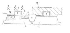
- a silicon substrate 1is shown, provided with an N-well region 2 and a P-well region 3 , separated by a field isolation 4 .
- the P-well region 3is to be provided with an NMOS transistor 5
- the N-well region 2is to be provided with a PMOS transistor 6 .
- Both the P-well region 3 and the N-well region 2are provided with a gate oxide 7 on which polysilicon gate electrodes 8 are formed.
- a short oxidation step equivalent to a few nanometers of oxide growthis advantageously carried out to cover the silicon substrate and the polysilicon gate electrodes 8 with an oxide layer 9 .
- a hard mask layer 10(FIG. 2) of Ge-doped polycrystalline (poly-Si 0.65 Ge 0.35 ) is applied by chemical vapour deposition at 450° C. The layer is applied in a thickness of about 0.15 micron.
- a customarily used photoresist layer 11(thickness about 0.5 micron) is applied on top of the hard mask layer 10 and patterned using conventional lithography. The patterned resist layer 11 is used as a mask for patterning the hard mask layer 10 by means of plasma etching, the ultimate result of which is shown in FIG. 3 .
- FIG. 4shows the step wherein arsenic ions are implanted into the P-well region 3 at an energy in the range from 5 to 15 KeV and a dose in the range between 1E15 and 5E15 cm ⁇ 2 , preferably between 3E14 and 1E15 cm ⁇ 2 , which implantation step is followed by conventional annealing, thereby forming a source and a drain 12 .
- FIG. 5shows the pocket implantation using boron ions (15-30 KeV; 1E13-1E14 cm ⁇ 2 ) at a tilt angle of 20-40°, followed by an annealing step. The steps shown in FIGS. 4 and 5 can optionally be reversed, so that first a pocket implant/annealing is carried out followed by a source/drain implant/annealing.
- the hard mask 10is selectively removed from the wafer (not shown). If desired, The same steps as depicted in FIGS. 2 to 5 can be carried out for the N-well region 2 , using B or BF 2 ions for the source/drain implant and As or P ions for the pocket implant.
- the selectively implanted structureis subjected to conventional further processing to complete the semiconductor device comprising the PMOS transistor and the NMOS transistor. More in particular, side wall spacers, generally of oxides or nitrides, are formed on the sides of the gate electrodes. Subsequently the NMOS area is selectively doped with, generally, arsenic, while using conventional mask technologies, and the PMOS area is selectively doped with, generally, boron. The NMOS and PMOS doping steps can be carried out in any order. Then, an annealing step is carried out to activate the doped regions. Finally, conventional silicidation and metallisation steps are carried out, which ultimately provide the desired semiconductor device.
- side wall spacersgenerally of oxides or nitrides
Landscapes
- Physics & Mathematics (AREA)
- High Energy & Nuclear Physics (AREA)
- Engineering & Computer Science (AREA)
- General Physics & Mathematics (AREA)
- Computer Hardware Design (AREA)
- Toxicology (AREA)
- Crystallography & Structural Chemistry (AREA)
- Condensed Matter Physics & Semiconductors (AREA)
- Chemical & Material Sciences (AREA)
- Manufacturing & Machinery (AREA)
- Health & Medical Sciences (AREA)
- Microelectronics & Electronic Packaging (AREA)
- Power Engineering (AREA)
- Metal-Oxide And Bipolar Metal-Oxide Semiconductor Integrated Circuits (AREA)
- Electrodes Of Semiconductors (AREA)
- Crystals, And After-Treatments Of Crystals (AREA)
- Insulated Gate Type Field-Effect Transistor (AREA)
Abstract
Description
Claims (6)
Applications Claiming Priority (3)
| Application Number | Priority Date | Filing Date | Title |
|---|---|---|---|
| EP00201317 | 2000-04-12 | ||
| EP00201317 | 2000-04-12 | ||
| EP00201317.5 | 2000-04-12 |
Publications (2)
| Publication Number | Publication Date |
|---|---|
| US20010031522A1 US20010031522A1 (en) | 2001-10-18 |
| US6461908B2true US6461908B2 (en) | 2002-10-08 |
Family
ID=8171339
Family Applications (1)
| Application Number | Title | Priority Date | Filing Date |
|---|---|---|---|
| US09/829,796Expired - LifetimeUS6461908B2 (en) | 2000-04-12 | 2001-04-10 | Method of manufacturing a semiconductor device |
Country Status (8)
| Country | Link |
|---|---|
| US (1) | US6461908B2 (en) |
| EP (1) | EP1275147B1 (en) |
| JP (1) | JP4846167B2 (en) |
| KR (1) | KR100796825B1 (en) |
| AT (1) | ATE434831T1 (en) |
| DE (1) | DE60139068D1 (en) |
| TW (1) | TW533482B (en) |
| WO (1) | WO2001080310A1 (en) |
Cited By (10)
| Publication number | Priority date | Publication date | Assignee | Title |
|---|---|---|---|---|
| US6784062B2 (en)* | 2002-06-03 | 2004-08-31 | Micron Technology, Inc. | Transistor formation for semiconductor devices |
| US20060198028A1 (en)* | 2005-02-04 | 2006-09-07 | Carl Zeiss Smt Ag | Refractive optical imaging system, in particular projection objective for microlithography |
| US20070054449A1 (en)* | 2005-08-23 | 2007-03-08 | Macronix International Co. Ltd. | Methods of forming charge-trapping dielectric layers for semiconductor memory devices |
| US20080198353A1 (en)* | 2004-03-30 | 2008-08-21 | Carl Zeiss Smt Ag | Projection Objective, Projection Exposure Apparatus and Reflective Reticle For Microlithography |
| US20080252987A1 (en)* | 2004-08-06 | 2008-10-16 | Carl Zeiss Smt Ag | Projection Objective For Microlithography |
| US20100330756A1 (en)* | 2009-06-25 | 2010-12-30 | International Business Machines Corporation | Integrated circuit structure manufacturing methods using hard mask and photoresist combination |
| US20120153354A1 (en)* | 2010-12-21 | 2012-06-21 | Globalfoundries Inc. | Performance enhancement in transistors comprising high-k metal gate stacks and an embedded stressor by performing a second epitaxy step |
| US9305590B2 (en) | 2007-10-16 | 2016-04-05 | Seagate Technology Llc | Prevent data storage device circuitry swap |
| US9679602B2 (en) | 2006-06-14 | 2017-06-13 | Seagate Technology Llc | Disc drive circuitry swap |
| CN115064534A (en)* | 2022-07-12 | 2022-09-16 | 上海积塔半导体有限公司 | A kind of semiconductor device and preparation method thereof |
Families Citing this family (3)
| Publication number | Priority date | Publication date | Assignee | Title |
|---|---|---|---|---|
| JP3730947B2 (en)* | 2002-10-08 | 2006-01-05 | 松下電器産業株式会社 | Manufacturing method of semiconductor device |
| KR100779395B1 (en)* | 2006-08-31 | 2007-11-23 | 동부일렉트로닉스 주식회사 | Semiconductor device and manufacturing method |
| US8877596B2 (en)* | 2010-06-24 | 2014-11-04 | International Business Machines Corporation | Semiconductor devices with asymmetric halo implantation and method of manufacture |
Citations (5)
| Publication number | Priority date | Publication date | Assignee | Title |
|---|---|---|---|---|
| JPS5513953A (en) | 1978-07-18 | 1980-01-31 | Fujitsu Ltd | Complementary integrated circuit |
| US5227321A (en) | 1990-07-05 | 1993-07-13 | Micron Technology, Inc. | Method for forming MOS transistors |
| US5904520A (en)* | 1998-01-05 | 1999-05-18 | Utek Semiconductor Corp. | Method of fabricating a CMOS transistor |
| US5930615A (en) | 1995-11-27 | 1999-07-27 | Micron Technology, Inc. | Method of forming CMOS having simultaneous formation of halo regions of PMOS and part of source/drain of NMOS |
| US6187619B1 (en)* | 1998-02-17 | 2001-02-13 | Shye-Lin Wu | Method to fabricate short-channel MOSFETs with an improvement in ESD resistance |
Family Cites Families (12)
| Publication number | Priority date | Publication date | Assignee | Title |
|---|---|---|---|---|
| JPS5651872A (en)* | 1979-10-05 | 1981-05-09 | Oki Electric Ind Co Ltd | Manufacture of complementary type mos transistor |
| JPH01145849A (en)* | 1987-12-01 | 1989-06-07 | Fujitsu Ltd | Manufacture of semiconductor device |
| JPH029164A (en)* | 1988-06-28 | 1990-01-12 | Matsushita Electric Ind Co Ltd | Pattern forming method and semiconductor device manufacturing method |
| JPH02162739A (en)* | 1988-12-15 | 1990-06-22 | Fujitsu Ltd | Manufacturing method of semiconductor device |
| JP2917696B2 (en)* | 1992-08-22 | 1999-07-12 | 日本電気株式会社 | Method for manufacturing CMOS semiconductor device |
| JP3062398B2 (en)* | 1993-06-25 | 2000-07-10 | 松下電器産業株式会社 | Method for manufacturing CMOS semiconductor device |
| US5292681A (en)* | 1993-09-16 | 1994-03-08 | Micron Semiconductor, Inc. | Method of processing a semiconductor wafer to form an array of nonvolatile memory devices employing floating gate transistors and peripheral area having CMOS transistors |
| US5489546A (en)* | 1995-05-24 | 1996-02-06 | Micron Technology, Inc. | Method of forming CMOS devices using independent thickness spacers in a split-polysilicon DRAM process |
| US6004854A (en)* | 1995-07-17 | 1999-12-21 | Micron Technology, Inc. | Method of forming CMOS integrated circuitry |
| JPH09205151A (en)* | 1996-01-26 | 1997-08-05 | Sony Corp | Manufacture of complementary semiconductor device |
| JP2980057B2 (en)* | 1997-04-30 | 1999-11-22 | 日本電気株式会社 | Method for manufacturing semiconductor device |
| US5920774A (en)* | 1998-02-17 | 1999-07-06 | Texas Instruments - Acer Incorporate | Method to fabricate short-channel MOSFETS with an improvement in ESD resistance |
- 2001
- 2001-04-03KRKR1020017015928Apatent/KR100796825B1/ennot_activeExpired - Fee Related
- 2001-04-03ATAT01938077Tpatent/ATE434831T1/ennot_activeIP Right Cessation
- 2001-04-03JPJP2001577605Apatent/JP4846167B2/ennot_activeExpired - Fee Related
- 2001-04-03EPEP01938077Apatent/EP1275147B1/ennot_activeExpired - Lifetime
- 2001-04-03DEDE60139068Tpatent/DE60139068D1/ennot_activeExpired - Lifetime
- 2001-04-03WOPCT/EP2001/003749patent/WO2001080310A1/enactiveApplication Filing
- 2001-04-10USUS09/829,796patent/US6461908B2/ennot_activeExpired - Lifetime
- 2001-04-19TWTW090109425Apatent/TW533482B/enactive
Patent Citations (5)
| Publication number | Priority date | Publication date | Assignee | Title |
|---|---|---|---|---|
| JPS5513953A (en) | 1978-07-18 | 1980-01-31 | Fujitsu Ltd | Complementary integrated circuit |
| US5227321A (en) | 1990-07-05 | 1993-07-13 | Micron Technology, Inc. | Method for forming MOS transistors |
| US5930615A (en) | 1995-11-27 | 1999-07-27 | Micron Technology, Inc. | Method of forming CMOS having simultaneous formation of halo regions of PMOS and part of source/drain of NMOS |
| US5904520A (en)* | 1998-01-05 | 1999-05-18 | Utek Semiconductor Corp. | Method of fabricating a CMOS transistor |
| US6187619B1 (en)* | 1998-02-17 | 2001-02-13 | Shye-Lin Wu | Method to fabricate short-channel MOSFETs with an improvement in ESD resistance |
Cited By (16)
| Publication number | Priority date | Publication date | Assignee | Title |
|---|---|---|---|---|
| US6784062B2 (en)* | 2002-06-03 | 2004-08-31 | Micron Technology, Inc. | Transistor formation for semiconductor devices |
| US20080198353A1 (en)* | 2004-03-30 | 2008-08-21 | Carl Zeiss Smt Ag | Projection Objective, Projection Exposure Apparatus and Reflective Reticle For Microlithography |
| US8064040B2 (en) | 2004-03-30 | 2011-11-22 | Carl Zeiss Smt Gmbh | Projection objective, projection exposure apparatus and reflective reticle for microlithography |
| US20080252987A1 (en)* | 2004-08-06 | 2008-10-16 | Carl Zeiss Smt Ag | Projection Objective For Microlithography |
| US8212988B2 (en) | 2004-08-06 | 2012-07-03 | Carl Zeiss GmbH | Projection objective for microlithography |
| US9217932B2 (en) | 2004-08-06 | 2015-12-22 | Carl Zeiss Smt Gmbh | Projection objective for microlithography |
| US9568838B2 (en) | 2004-08-06 | 2017-02-14 | Carl Zeiss Smt Gmbh | Projection objective for microlithography |
| US7511890B2 (en) | 2005-02-04 | 2009-03-31 | Carl Zeiss Smt Ag | Refractive optical imaging system, in particular projection objective for microlithography |
| US20060198028A1 (en)* | 2005-02-04 | 2006-09-07 | Carl Zeiss Smt Ag | Refractive optical imaging system, in particular projection objective for microlithography |
| US20070054449A1 (en)* | 2005-08-23 | 2007-03-08 | Macronix International Co. Ltd. | Methods of forming charge-trapping dielectric layers for semiconductor memory devices |
| US7704865B2 (en)* | 2005-08-23 | 2010-04-27 | Macronix International Co., Ltd. | Methods of forming charge-trapping dielectric layers for semiconductor memory devices |
| US9679602B2 (en) | 2006-06-14 | 2017-06-13 | Seagate Technology Llc | Disc drive circuitry swap |
| US9305590B2 (en) | 2007-10-16 | 2016-04-05 | Seagate Technology Llc | Prevent data storage device circuitry swap |
| US20100330756A1 (en)* | 2009-06-25 | 2010-12-30 | International Business Machines Corporation | Integrated circuit structure manufacturing methods using hard mask and photoresist combination |
| US20120153354A1 (en)* | 2010-12-21 | 2012-06-21 | Globalfoundries Inc. | Performance enhancement in transistors comprising high-k metal gate stacks and an embedded stressor by performing a second epitaxy step |
| CN115064534A (en)* | 2022-07-12 | 2022-09-16 | 上海积塔半导体有限公司 | A kind of semiconductor device and preparation method thereof |
Also Published As
| Publication number | Publication date |
|---|---|
| EP1275147B1 (en) | 2009-06-24 |
| DE60139068D1 (en) | 2009-08-06 |
| KR100796825B1 (en) | 2008-01-22 |
| JP4846167B2 (en) | 2011-12-28 |
| TW533482B (en) | 2003-05-21 |
| EP1275147A1 (en) | 2003-01-15 |
| KR20020025892A (en) | 2002-04-04 |
| JP2003531494A (en) | 2003-10-21 |
| ATE434831T1 (en) | 2009-07-15 |
| US20010031522A1 (en) | 2001-10-18 |
| WO2001080310A1 (en) | 2001-10-25 |
Similar Documents
| Publication | Publication Date | Title |
|---|---|---|
| US9024384B2 (en) | Indium, carbon and halogen doping for PMOS transistors | |
| US6306712B1 (en) | Sidewall process and method of implantation for improved CMOS with benefit of low CGD, improved doping profiles, and insensitivity to chemical processing | |
| US5963803A (en) | Method of making N-channel and P-channel IGFETs with different gate thicknesses and spacer widths | |
| US5969407A (en) | MOSFET device with an amorphized source | |
| US20070187757A1 (en) | Semiconductor devices and methods of fabricating the same | |
| WO1999050900A1 (en) | Reduced channel length lightly doped drain transistor using a sub-amorphous large tilt angle implant to provide enhanced lateral diffusion | |
| US8853042B2 (en) | Carbon and nitrogen doping for selected PMOS transistors on an integrated circuit | |
| JP2005524243A (en) | Metal gate electrode using silicide and method of forming the same | |
| US6461908B2 (en) | Method of manufacturing a semiconductor device | |
| US20060273409A1 (en) | High performance CMOS with metal-gate and Schottky source/drain | |
| JP2004508717A5 (en) | ||
| US6362062B1 (en) | Disposable sidewall spacer process for integrated circuits | |
| US6194293B1 (en) | Channel formation after source and drain regions are formed | |
| US20060273391A1 (en) | CMOS devices for low power integrated circuits | |
| US6380021B1 (en) | Ultra-shallow junction formation by novel process sequence for PMOSFET | |
| US7163878B2 (en) | Ultra-shallow arsenic junction formation in silicon germanium | |
| US20070020865A1 (en) | Multi-work function gates for CMOS circuit and method of manufacture | |
| JP2006060208A (en) | Source / drain structure for high performance sub-0.1 micrometer transistors | |
| US7122862B2 (en) | Reduction of channel hot carrier effects in transistor devices | |
| US6630386B1 (en) | CMOS manufacturing process with self-amorphized source/drain junctions and extensions | |
| US5937302A (en) | Method of forming lightly doped drain region and heavily doping a gate using a single implant step | |
| US9761689B2 (en) | Method of forming a semiconductor device and according semiconductor device | |
| CN120264797A (en) | Method for forming lightly doped drain region | |
| KR20050067730A (en) | Method for manufacturing dual gate electrode | |
| JP2001168332A (en) | Halo structure for use in transistors featuring reduced dimensions |
Legal Events
| Date | Code | Title | Description |
|---|---|---|---|
| AS | Assignment | Owner name:KONINKLIJKE PHILIPS ELECTRONICS N.V., NETHERLANDS Free format text:ASSIGNMENT OF ASSIGNORS INTEREST;ASSIGNORS:STOLK, PETER ADRIAAN;WOERLEE, PIERRE HERMANUS;KNITEL, MATHIJS JOHAN;AND OTHERS;REEL/FRAME:011865/0081;SIGNING DATES FROM 20010503 TO 20010508 | |
| STCF | Information on status: patent grant | Free format text:PATENTED CASE | |
| FPAY | Fee payment | Year of fee payment:4 | |
| AS | Assignment | Owner name:NXP B.V., NETHERLANDS Free format text:ASSIGNMENT OF ASSIGNORS INTEREST;ASSIGNOR:KONINKLIJKE PHILIPS ELECTRONICS N.V.;REEL/FRAME:018635/0787 Effective date:20061117 | |
| FPAY | Fee payment | Year of fee payment:8 | |
| AS | Assignment | Owner name:NXP B.V., NETHERLANDS Free format text:CHANGE OF NAME;ASSIGNOR:PHILIPS SEMICONDUCTORS INTERNATIONAL B.V.;REEL/FRAME:026837/0649 Effective date:20060929 | |
| AS | Assignment | Owner name:CALLAHAN CELLULAR L.L.C., DELAWARE Free format text:ASSIGNMENT OF ASSIGNORS INTEREST;ASSIGNOR:NXP B.V.;REEL/FRAME:027265/0798 Effective date:20110926 | |
| FEPP | Fee payment procedure | Free format text:PAYOR NUMBER ASSIGNED (ORIGINAL EVENT CODE: ASPN); ENTITY STATUS OF PATENT OWNER: LARGE ENTITY Free format text:PAYER NUMBER DE-ASSIGNED (ORIGINAL EVENT CODE: RMPN); ENTITY STATUS OF PATENT OWNER: LARGE ENTITY | |
| FPAY | Fee payment | Year of fee payment:12 | |
| AS | Assignment | Owner name:M-RED INC., TEXAS Free format text:ASSIGNMENT OF ASSIGNORS INTEREST;ASSIGNOR:INTELLECTUAL VENTURES ASSETS 108 LLC;REEL/FRAME:048662/0318 Effective date:20190315 Owner name:INTELLECTUAL VENTURES ASSETS 108 LLC, DELAWARE Free format text:ASSIGNMENT OF ASSIGNORS INTEREST;ASSIGNOR:CALLAHAN CELLULAR L.L.C.;REEL/FRAME:048666/0844 Effective date:20190222 |