US6461801B1 - Rapid heating and cooling of workpiece chucks - Google Patents
Rapid heating and cooling of workpiece chucksDownload PDFInfo
- Publication number
- US6461801B1 US6461801B1US09/579,943US57994300AUS6461801B1US 6461801 B1US6461801 B1US 6461801B1US 57994300 AUS57994300 AUS 57994300AUS 6461801 B1US6461801 B1US 6461801B1
- Authority
- US
- United States
- Prior art keywords
- temperature
- chuck
- workpiece
- heat transfer
- fluid
- Prior art date
- Legal status (The legal status is an assumption and is not a legal conclusion. Google has not performed a legal analysis and makes no representation as to the accuracy of the status listed.)
- Expired - Lifetime
Links
Images


Classifications
- H—ELECTRICITY
- H01—ELECTRIC ELEMENTS
- H01L—SEMICONDUCTOR DEVICES NOT COVERED BY CLASS H10
- H01L21/00—Processes or apparatus adapted for the manufacture or treatment of semiconductor or solid state devices or of parts thereof
- H01L21/67—Apparatus specially adapted for handling semiconductor or electric solid state devices during manufacture or treatment thereof; Apparatus specially adapted for handling wafers during manufacture or treatment of semiconductor or electric solid state devices or components ; Apparatus not specifically provided for elsewhere
- H01L21/67005—Apparatus not specifically provided for elsewhere
- H01L21/67011—Apparatus for manufacture or treatment
- H01L21/67098—Apparatus for thermal treatment
- H01L21/67109—Apparatus for thermal treatment mainly by convection
- H—ELECTRICITY
- H01—ELECTRIC ELEMENTS
- H01L—SEMICONDUCTOR DEVICES NOT COVERED BY CLASS H10
- H01L21/00—Processes or apparatus adapted for the manufacture or treatment of semiconductor or solid state devices or of parts thereof
- H01L21/67—Apparatus specially adapted for handling semiconductor or electric solid state devices during manufacture or treatment thereof; Apparatus specially adapted for handling wafers during manufacture or treatment of semiconductor or electric solid state devices or components ; Apparatus not specifically provided for elsewhere
- H01L21/683—Apparatus specially adapted for handling semiconductor or electric solid state devices during manufacture or treatment thereof; Apparatus specially adapted for handling wafers during manufacture or treatment of semiconductor or electric solid state devices or components ; Apparatus not specifically provided for elsewhere for supporting or gripping
- H01L21/687—Apparatus specially adapted for handling semiconductor or electric solid state devices during manufacture or treatment thereof; Apparatus specially adapted for handling wafers during manufacture or treatment of semiconductor or electric solid state devices or components ; Apparatus not specifically provided for elsewhere for supporting or gripping using mechanical means, e.g. chucks, clamps or pinches
- H01L21/68714—Apparatus specially adapted for handling semiconductor or electric solid state devices during manufacture or treatment thereof; Apparatus specially adapted for handling wafers during manufacture or treatment of semiconductor or electric solid state devices or components ; Apparatus not specifically provided for elsewhere for supporting or gripping using mechanical means, e.g. chucks, clamps or pinches the wafers being placed on a susceptor, stage or support
Definitions
- the present inventionrelates generally to temperature control of workpiece supports for semiconductor processing equipment, and more particularly to rapid heating and cooling of such chucks for resist stripping chambers.
- a workpiecee.g., a silicon wafer, glass substrate, etc.
- Gaseous and/or plasma reactantsare supplied to the surface of the workpiece while the workpiece is heated to specific temperatures.
- radiant heatmay be supplied to the workpiece through transparent “cold walls” formed of quartz. Radiant heat is particularly used for very high temperature processing (e.g., at greater than 500° C.), where it is desirable to raise and lower temperature during the process cycle for each workpiece.
- the temperature of the workpiece supportcan be regulated by resistive heating.
- chucksrefer to supports for processing workpieces that are kept at constant temperature as workpieces transferred in, processed and transferred out in cycles.
- a processed workpieceis advantageously allowed to cool to less than about 70° C. prior to placement in a low cost storage cassette that would otherwise melt. Since processing time within the chamber is at a premium, such cooling is most typically performed outside of the chamber on a separate station, such that another workpiece can be introduced to the process chamber while the first workpiece is cooling. Workpiece temperature ramping is thereby minimized, as the massive chuck is maintained at a substantially constant temperature while multiple workpieces are sequentially processed.
- a chuckfor supporting a workpiece within a semiconductor processing chamber.
- the chuckis provided with temperature control mechanisms that permit rapid heating or cooling of the chuck during processing.
- an apparatusfor controlling the temperature of workpieces in a semiconductor processing reactor.
- the apparatusincludes a support with fluid channels.
- a cold fluid sourcecommunicates with the fluid channels via a first supply line, and is configured to maintain a cold fluid maintained at a first temperature.
- a heat sourceis maintained at a second temperature, which is higher than the first temperature.
- a mechanismis provided for conductively transferring heat from the heat source to the support.
- a methodfor controlling a workpiece chuck temperature in a process chamber.
- a first heat transfer fluidcirculates through the chuck during a cold phase to bring the chuck to a first temperature.
- the first heat transfer fluidis removed from the chuck during a hot phase.
- the chuckis heated to a second temperature higher than the first temperature.
- both a high temperature fluid source and a low temperature fluid sourceare connected to the fluid channels.
- a relatively low temperature fluidis supplied to the fluid channels in the wafer chuck during at least a portion of each cycle.
- a heater blockis in close contact with the chuck.
- the heater blockis physically moved from contact with the chuck and lower temperature heat transfer fluid flows through the chuck.
- the dual temperature chucks of the preferred embodimentscan be used in a photoresist-stripping reactor.
- cool fluidis utilized to rapidly reduce workpiece temperature before removing the workpiece from the chuck.
- low temperature fluidis kept at a temperature appropriate for a cleaning process, while a high temperature fluid supply or a heater block is kept at a high temperature suitable for photoresist stripping.
- other multiple-step processes, particularly including photoresist strippingcan be conducted at different temperatures rapidly and efficiently using the same wafer chuck.
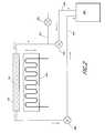
- FIG. 1is a schematic view of a dual temperature workpiece chuck having a cold fluid source and a hot fluid source, constructed in accordance with a first preferred embodiment of the present invention
- FIG. 2is a schematic view of a dual temperature workpiece chuck having a cold fluid source and a movable heater block, constructed in accordance with a second preferred embodiment of the present invention.
- a workpiece support apparatus or wafer chuck 50is provided with fluid flow channels 15 .
- the channelscan be connected in series to define a single flow path winding through the chuck.
- the fluid channels 15preferably occupy at least about 50% of the wafer chuck volume, more preferably at least about 70%.
- the fluid channels 15can be provided in the wafer chuck 10 in a variety of manners.
- the fluid channels 15can be machined into a metal block from which the chuck 10 is formed, or the channels 15 can be formed in a molding process.
- the chuck 10can be formed of two pieces, with machined surface channels (not shown) in one piece covered by the other piece.
- surface channelscan be formed in a lower piece, with mating surface channels in the upper piece.
- the chuck 10can have any suitable construction, and in the illustrated embodiment provides an electrostatic attractive force for holding a workpiece (not shown) in place.
- the chuck 10can include vacuum channels for holding the workpiece to the chuck 10 .
- a workpieceis held solely by gravitational forces on a susceptor or other support means.
- the body of the chuck 10is desirably formed of a thermally conductive material, and in the illustrated embodiment is formed of aluminum alloy.
- a reactor (not shown) of the preferred embodimentincludes mechanisms for maintaining the chuck 10 at two different temperatures at different stages or phases of a process cycle.
- the mechanisms of the reactorare configured to rapidly exchange heat with the chuck 10 , effectively raising or lowering its temperature.
- the chuck/workpiece combinationrapidly reaches and maintains a desirable high or low temperature.
- a high temperature mechanism or heat sourcecomprises a hot fluid source 20 that is connected to the fluid channels 15 within the wafer chuck 10 by way of a supply line 22 and a return line 24 .
- a switch to bring the heat source into thermal communication with the chuck 10includes switching valves 26 and 28 along each of the supply 22 and return lines 24 , desirably centrally controlled to switch between the hot fluid source 20 and a cold fluid source 40 that will be discussed in more detail below. While not illustrated, it will be understood that the system includes pumping means for circulating fluid through the wafer chuck 10 .
- purge source 30is connected to the supply line 22 between the hot fluid source and the wafer chuck 10 .
- a purge line 32supplies a non-reactive or inert gas from the purge source 30 to the supply line 22 by way of a two-way valve or purge valve 35 , which is advantageously also centrally controlled.
- the illustrated purge gasis nitrogen (N 2 ).
- suitable purge gasesinclude argon (Ar), helium (He), hydrogen (H 2 ), and other gases which are non-reactive with the heat transfer fluid and with the material of the wafer chuck 10 . It will be understood that a liquid can also be used for purging, though that is less preferred.
- the hot fluid source 20desirably holds a heat transfer fluid, the composition of which may vary with the application.
- the boiling point of the heat transfer fluidis preferably greater than about 200° C., more preferably greater than about 250° C.
- Preferred examplesinclude a fluid commercially available under the trade name Paratherm NFTM from Paratherm Corporation of Conshohocken, Pa.
- Another suitable thermal transfer fluidcomprises DowthermTM, commercially available from the Dow Chemical Company of Midland, Mo. These fluids operate efficiently for heat transfer at temperatures up to about 400° C.
- Galden-HT270from the Kurt J. Lesker Company of Clairton, Pa., is preferably used for electrostatic chucks due to its superior dielectric properties. It can be operated at temperatures of up to about 270° C.
- a cold sourcecomprises a cold fluid source 40 that is also connected to the fluid channels 15 within the wafer chuck 10 via a supply line 42 and a return lines 44 .
- coldrefers only to the temperature of the cold fluid source 40 relative to the temperature of the hot fluid source 20 .
- the actual “cold” fluid source 40is heated to a temperature above room temperature.
- the cold fluid source 40is connected to the same fluid channels 15 in the wafer chuck 10 as the hot fluid source 20 , thus maximizing the thermal mass of either the hot or cold heat transfer fluid, depending upon the point in the cycle, that can be flowed through the chuck 10 .
- the cold fluid source 40includes switchable valves 26 , 28 on each of the return line 44 and the supply line 42 .
- the valvescomprise the same three-way switching valves 26 , 28 that also connect to the supply and return lines 22 , 24 of the hot fluid source 20 .
- the supply and return lines 22 , 24 , 42 , 44 for the hot and cold fluid sources 20 , 40include common sections (common supply line section 50 and common return line section 52 ) between the three-way switching valves 26 , 28 and the wafer chuck 10 .
- the supply lines 22 , 42each include the common supply line section 50 and the return lines 24 , 44 each include the common return line section 52 .
- the heat transfer fluid within the cold fluid source 40comprises the same type of fluid held in the hot fluid source 20 , thus avoiding problems of cross-contamination and reaction between the fluids.
- the cold fluidis maintained at temperatures less than about 150° C., and for certain embodiments more preferably less than 100° C. or less than 50° C., depending upon the purpose of the cold fluid source 40 .
- the cold fluidis preferably kept at a temperature range less than about 100° C., and more preferably less than about 70° C.
- the cold fluidis preferably maintained at or slightly above the desirable workpiece temperature.
- Fluid temperature in each of the hot fluid source 20 and the cold fluid source 40can be maintained at their respective desirable temperatures by any of a variety of suitable heating or cooling means, as will be readily understood by one of ordinary skill in the art.
- both the hot and cold fluid sources 20 , 40are heated above room temperature.
- the cold fluid source 40serves only to lower workpiece temperature prior to transfer to a storage cassette, the cold fluid can be maintained below room temperature.
- the skilled artisancan readily determine, for a particular wafer chuck 10 configuration, the appropriate temperature at which to keep the heat transfer fluid in order for the workpiece to be kept at the desired temperature.
- Factors affecting a temperature differential between the cold or hot fluid source 40 or 20 and the workpiece temperatureinclude heat losses (or gains) along the return lines 24 , 44 and supply lines 22 , 42 , as well as other losses to the environment within the reactor.
- fluid from the hot fluid source 20is preferably circulated through the hot supply line 22 , the first or supply-end three-way switching valve 26 , the common supply line section 50 , the fluid channels 15 , the common return line section 52 , the second or return-end three-way switching valve 28 , the hot return line 24 and back to the hot fluid source 20 .
- the switchis activated to bring the heat source in thermal communication with the chuck. Namely, the supply-end three-way switching valve 26 along the hot supply line 22 is closed, and the purge valve 35 to the purge line 30 is opened.
- Purge gassuch as nitrogen gas (N 2 ) in the illustrated embodiment, then flows under pressure through the fluid channels 15 in the wafer chuck 10 , thereby blowing residual hot fluid out through the hot return line 24 back into the hot fluid source 20 .
- the return-end three-way switching valve 28 at the juncture of the return lines 24 , 44can be switched to allow purged heat transfer fluid to the cold fluid source 40 .
- the volume of fluid in the cold fluid source 40is preferably large enough that the purged hot fluid has little effect on the overall temperature of the cold fluid source 40 .
- the purge valve 35is switched off and the supply-end switching valve 26 at the juncture of the supply lines 22 , 42 is switched to allow flow from the cold fluid source 40 through the wafer chuck 10 .
- the switching valve between the return lines 40 a and 40 bis switched to allow flow of cold fluid back to the cold fluid source 20 from the wafer chuck 50 .
- the supply-end three-way switching valve 26is again switched to an off position, while the purge valve 35 is opened to once again purge fluid from the wafer chuck 10 .
- the cold fluidcan be purged to the hot fluid source 20 , but is preferably purged to its originating cold fluid source 40 .
- the cycleis then repeated by switching the valves 26 , 28 again to allow flow from the hot fluid source 20 .
- the purge line 30can be eliminated from the system of FIG. 1, particularly if the hot fluid source 20 and the cold fluid source 40 comprise the same heat transfer fluid.
- hot heat transfer fluidcan be purged with cold heat transfer fluid, without the intermediate gas purge step.
- the mass of the hot fluid source 20is desirably high enough that mixing of purged cold fluid has negligible effect on the temperature of the stored hot fluid.
- the mass of the cold fluid source 40is desirably high enough that mixing of purged hot fluid with the cold fluid source 40 has negligible effect on the temperature of the stored cold fluid.
- the volume of fluid in each of the hot fluid source 20 and the cold fluid source 40is greater than about five (5) times the volume of the purged fluid (representing a volume of fluid within the supply lines 22 , 42 and return lines 24 , 44 and within the fluid channels 15 in the wafer chuck 10 ). More preferably, the fluid sources 20 , 40 are each greater than about ten (10) times and most preferably greater than about twenty (20) times the volume of purged fluid.
- the workpiece support of the second embodimentalso comprises a wafer chuck 10 a including fluid channels 15 a .
- a cold fluid source 40 astoring thermal transfer fluid at a relatively low temperature, circulates cold heat transfer fluid through the fluid channels 15 a in the wafer chuck 10 a via a supply line 42 a and a return line 44 a .
- the cold fluid source 40 acan be as described with respect to the previous embodiment.
- the second embodimentalso includes a purge line 32 a in communication with the supply line 42 a via an on/off purge valve 35 a.
- the heat source of the second embodimentis a movable electrically heated chuck or heater block 20 a , as illustrated in FIG. 2 .
- the heater block 20 ais movable relative to the wafer chuck 10 a , although it will be understood that, in some arrangements, the wafer chuck 10 a can be made movable while the heater block 20 a remains stationary.
- a switch for selectively bringing the heat source into thermal communication with the chuckthus comprises an actuator (not shown) that activates the motor for moving the heater block 20 a . It will be understood, of course, that the chuck could be moved while the heater block is stationary.
- the heater block 20 ais preferably maintained during processing at a hot or process temperature that is equal to or slightly above the desired workpiece temperature for a high temperature integrated circuit fabrication process, much in the way that the heat transfer fluid within the hot fluid source 20 of FIG. 1 is constantly maintained at the desired high temperature.
- the heater block 20 acan be maintained at a desired high temperature by any of a variety of suitable means.
- the heater block 20 acan be heated by fluid convection, where heat transfer fluid heated in a hot fluid source is circulated through the heater block 20 a , much in the way that the wafer chuck 10 is directly heated by fluid convection in the embodiment of FIG. 1 .
- the heater block 20 ais maintained at a high temperature by electrical or resistive heating.
- the heater block 20 acan be radiantly heated, inductively heated, etc.
- the heater block 20 ahas a high thermal mass relative to the supporting portion of the wafer chuck 10 a .
- the thermal mass of the heater block 20 ais greater than that of the wafer chuck 10 a , more preferably greater than about 5 times and most preferably greater than about 10 times the thermal mass of the wafer chuck 10 a.
- the heater block 20 aIn operation, when a wafer or other workpiece supported upon the chuck 10 a is ready for high temperature processing, the heater block 20 a is positioned for conductive heat transfer between the heater block 20 a and the chuck 10 a . Preferably, the heater block 20 a directly contacts the chuck 10 a , more preferably flush across major surfaces of the heater block 20 a and the backside of the chuck 10 a.
- the heater block 20 aWhen it is desired to cool the wafer to a cold or lower temperature, the heater block 20 a is removed from the thermally conductive position. In the illustrated embodiment, the heater block 20 a is lowered from the chuck 10 a , preferably by a distance of at least about 0.25 inch, and more preferably by a distance of about 0.5 inch. At the same time, or slightly after removal of the heater block 20 a , the valves 26 a , 28 a on the supply and return lines 42 a , 44 a to the cold fluid source 40 a are opened, and cold fluid is circulated through the lines and the wafer chuck 10 a . The chuck 10 a is thereby quickly cooled to approximately the temperature of the cold fluid source 40 a . It will also be understood that the lower the thermal mass of the chuck 10 a , particularly in relation to the heater block 20 a , the quicker the chuck temperature can be changed.
- a lower temperature process phaseis conducted on the workpiece seated on the chuck 10 a .
- the cooled workpiececan be removed from the chuck 10 a at this stage and placed in a low-cost storage cassette without waiting for further cooling, and without the need for separate workpiece cooling mechanisms (such as cooling stations utilized in many semiconductor processing systems).
- the valve 26 a on the supply line 42 a from the cold fluid source 40 ais closed, and the valve 35 a on the purge line 32 a is opened to allow gas flow through the fluid channels 15 a in the wafer chuck 10 a . Residual cold fluid is thereby purged from the channels 15 a in wafer chuck 10 a through the return line 44 a and back to the cold fluid source 40 a .
- the heater block 20 ais moved relative to the chuck 10 a to bring the heater block 20 a again in a position where heat is conductively exchanged from the heater block 20 a to the wafer chuck 10 a.
- the illustrated dual temperature wafer chucks 10 , 10 aare employed within a microwave plasma asher for stripping organic photoresist from integrated circuit workpieces.
- the reactorcan also employ an internal radio frequency (RF) plasma generator within the process chamber.
- RFradio frequency
- the wafer chuck 10 , 10 ais powered, as well as a portion of the chamber walls, producing a parallel plate arrangement suitable for reactive ion etching within the chamber.
- the dual temperature wafer chucks 10 , 10 a of the preferred embodimentsare particularly useful for photoresist stripping and/or cleaning operations within a microwave plasma ashing reactor, also known as a chemical downstream etch (CDE) reactor.
- CDEchemical downstream etch
- Photoresistis applied and removed from a workpiece at various stages of semiconductor fabrication.
- the illustrated dual temperature wafer chucks 10 , 10 ahave utility in many resist strip contexts.
- regions of a semiconductor substrateare implanted with dopants (e.g. boron, phosphorous, arsenic) through a photoresist mask.
- dopantse.g. boron, phosphorous, arsenic
- Ion implantationis similarly performed through masks in many other doping steps.
- the ion implantation processresults in a hardened crust at the top surface of the photoresist. Outgassing during high temperature steps tends to be trapped by the hardened crust until an explosive pressure is built within the photoresist, potentially causing damage to both the partially fabricated wafer as well as the reactor.
- utilizing a low temperature strip process to avoid excess gas build-uphas minimized this risk.
- an initial stripis first conducted at low temperature until the trapping crust is removed from the photoresist.
- Wafer temperatures during the initial stepare preferably kept between about 100° C. and 140° C., more preferably between about 110° C. and 125° C.
- Reaction gasescan include an oxidant to aid oxidation of the resist (e.g., O 2 , preferably converted to oxygen radicals); a fluorine source to aid removal of the implanted portion (e.g., NF 3 or CF 4 , preferably converted to fluorine radicals); and a diluting gas (such as He or Ar) and/or forming gas (H 2 /N 2 ) to serve as a carrier.
- Reactantscan be supplied to the workpiece surface in any suitable fashion. Radicals are preferably generated in a remote microwave plasma generator. The implanted upper portion of the resist is typically removed in about thirty (30) seconds.
- cold fluidis preferably circulated through the wafer chuck 10 , 10 a , and the cold fluid is desirably stored in the cold fluid source 40 , 4 a at the desired wafer temperatures (i.e., between about 100° C. and 140° C., more preferably between about 110° C. and 125° C.). Accordingly, the “cold” fluid is actually heated to the desired temperature.
- the cold fluidis purged from the wafer chuck 10 , preferably with a purge gas for about five (5) seconds, and the hot fluid is circulated through the wafer chuck 10 .
- switching temperaturesinvolves stopping the cold fluid flow through the heater chuck 10 a , purging the cold fluid from the chuck 10 a , and raising the heater block 20 a to conductive contact with the wafer chuck 10 a.
- the temperatureis raised to between about 150° C. and 300° C. and more preferably between about 200° C. and 250° C.
- the same reactant chemistrycan continue to flow during the second stage of the strip.
- N 2or forming gas
- O 2or fluorine flow
- the raised temperatureresults in a significantly increased etch rate, thereby improving workpiece throughput.
- a temperature of about 250° C.results in a strip rate of about 7 ⁇ m/min.
- a typical photoresist mask of about 1 ⁇ mcan therefore be removed within about 5 to 10 seconds.
- viasare created through layers, typically through insulating layers such as borophosphosilicate glass (BPSG) or oxides formed from tetraethylorthosilicate (TEOS).
- BPSGborophosphosilicate glass
- TEOStetraethylorthosilicate
- a photoresist maskis selectively exposed and developed in a desired pattern and the developed or undeveloped resist is removed, depending upon whether positive or negative resist is employed.
- Viasare then formed through the patterned photoresist mask and through the exposed portions of the underlying layer, typically an oxide.
- the photoresist maskAfter via formation, the photoresist mask must be removed. Unfortunately, the process of forming the via creates an organic residue within the via, which is often difficult to remove.
- the residueis often referred to in the industry as a polymer “veil,” and is particularly problematic following reactive ion etching of vias for back-end or metallization stages of fabrication. While relatively vigorous cleaning chemistries must be employed to remove this polymer residue, overetching risks damage to the exposed features within the via. Accordingly, it is advantageous to conduct the post-via formation cleaning, after rapid resist stripping, at relatively low temperatures.
- a high temperature resist stripcan be conducted at rapid rates, as disclosed above with respect to the second stage of the post-implant process. Reactants can also be as discussed above, with optional fluorine flow.
- hot fluidcan circulate through the wafer chuck 10 (FIG. 1) or a heater block 20 a can be positioned for conductive thermal exchange with the wafer chuck 10 a (FIG. 2 ).
- the post-via cleaningcan be conducted within the same process chamber as the resist strip. Accordingly, a low temperature cleaning process is conducted immediately following the resist strip process.
- hot fluid circulationis discontinued and purged from the fluid channels 15 , and subsequently replaced with cold heat transfer fluid.
- the heater block 20 ais removed from the wafer chuck 10 a and cold fluid begins to circulate through the wafer chuck 10 a.
- the workpiece temperatureis preferably kept between about room temperature and 100° C., more preferably between about 50° C. and 80° C.
- the chemistry during this processpreferably includes an oxidant (e.g., O 2 ), a diluting gas (e.g., He, Ar, and/or forming gas—N 2 /H 2 ), and a fluorine source gas (e.g., NF 3 or CF 4 ).
- the fluorinewhile aiding removal of the polymer, also attacks the oxide sidewalls of the via.
- the oxidant and fluorine reactantscomprise radicals formed upstream of the reaction chamber.
- the processpreferably includes RF plasma generation within the chamber, compensating for reduced temperatures during the process. N 2 or forming gas aid maintenance of the plasma discharge. Additionally, an optional physical sputter etch can be briefly applied immediately after treatment with the oxygen and fluorine sources.
- “cold” fluidis thus circulated through the wafer chuck 10 , 10 a , where the cold fluid source is kept within the desired workpiece temperature range.
- the workpieceis removed from the chamber, cold fluid circulation is discontinued and the cold fluid is purged from the fluid channels 15 , 15 a .
- the cold fluidis replaced with hot heat transfer fluid, while in the embodiment of FIG. 2, the heater block 20 a is positioned for thermally conductive exchange with the wafer chuck 10 a .
- the chuck 10 or 10 ais thus prepared for processing another wafer.
- Integrated circuitsinclude many dielectric elements for electrical isolation of conductive elements.
- a common material for such dielectric elementsis silicon oxide in various forms, although silicon nitride is also popular for many applications.
- the contact holes or openingsare formed through insulating layers known as interlevel dielectrics (ILDs). Opening contact holes to active areas within semiconductor substrates often expose insulative sidewall spacers over transistor gate electrodes. Such contact etches typically also expose sacrificial oxide over the substrate. In each of these examples, masks are employed to define the hole or via, and an etch process exposes oxide surfaces.
- ILDsinterlevel dielectrics
- Such oxide surfacesdefine dimensions selected by a circuit design.
- ICintegrated circuit
- a first stage of post-contact etch resist strippingis conducted at high temperatures (preferably between about 100° C. and 300° C., more preferably between about 200° C. and 250° C.), with the wafer supported upon a dual temperature wafer chuck 10 or 10 a (FIGS. 1, 2 ).
- An exemplary reactant flowincludes 1:10 ratios of N 2 :O 2 .
- the illustrated dual temperature wafer chucks 10 , 10 acan be employed to perform a lower temperature post-strip clean.
- fluorineaids in cleaning oxide surfaces of lithography by-products.
- a relative small percentage of fluorine gas sourcee.g., less than about 5% CF 4 ) is added to the flow.
- the cold fluid source 40 , 40 ais preferably maintained between about 15° C. and 100° C., more preferably between about 20° C. and 100° C., and most preferably between about 25° C. and 50° C.
- the post-strip cleancan be strictly controlled by limiting the time for which the RF electrodes are powered (e.g. for about 15 seconds).
- the disclosed dual temperature wafer chucks 10 or 10 acan advantageously increase workpiece throughput for any desired process, including single-temperature processes which are conducted at high temperatures.
- a rapid resist strip process(preferably between about 100° C. and 300° C., more preferably between about 200° C. and 250° C.) can be followed by lowering the wafer temperature, while still mounted upon the chuck 10 , 10 a , to levels tolerable by commercial storage cassettes.
- the wafer temperatureis lowered to less than about 100° C., and more preferably to less than about 70° C.
- the cold fluid source 40 , 40 acan be maintained at well below the desired removal temperature.
- a high temperature differential between the hot wafer chuck 10 or 10 a (after resist strip) and the cold fluid introduced to the fluid channels 15 , 15 aresults in very rapid cooling of the workpiece/chuck combination.
- the cold fluid source 40 , 40 ais preferably maintained below about 100° C., and more preferably below about 70° C. The workpiece can thus be removed from the chuck 10 , 10 a and placed directly into a low temperature storage cassette without any waiting beyond the time required to open the chamber gate valve and extend the transfer robot to lift the workpiece.
Landscapes
- Engineering & Computer Science (AREA)
- Physics & Mathematics (AREA)
- Condensed Matter Physics & Semiconductors (AREA)
- General Physics & Mathematics (AREA)
- Manufacturing & Machinery (AREA)
- Computer Hardware Design (AREA)
- Microelectronics & Electronic Packaging (AREA)
- Power Engineering (AREA)
- Container, Conveyance, Adherence, Positioning, Of Wafer (AREA)
- Drying Of Semiconductors (AREA)
Abstract
Description
Claims (17)
Priority Applications (2)
| Application Number | Priority Date | Filing Date | Title |
|---|---|---|---|
| US09/579,943US6461801B1 (en) | 1999-05-27 | 2000-05-26 | Rapid heating and cooling of workpiece chucks |
| US10/244,713US20030015294A1 (en) | 1999-05-27 | 2002-09-16 | Rapid heating and cooling of workpiece chucks |
Applications Claiming Priority (2)
| Application Number | Priority Date | Filing Date | Title |
|---|---|---|---|
| US13673899P | 1999-05-27 | 1999-05-27 | |
| US09/579,943US6461801B1 (en) | 1999-05-27 | 2000-05-26 | Rapid heating and cooling of workpiece chucks |
Related Child Applications (1)
| Application Number | Title | Priority Date | Filing Date |
|---|---|---|---|
| US10/244,713DivisionUS20030015294A1 (en) | 1999-05-27 | 2002-09-16 | Rapid heating and cooling of workpiece chucks |
Publications (1)
| Publication Number | Publication Date |
|---|---|
| US6461801B1true US6461801B1 (en) | 2002-10-08 |
Family
ID=22474151
Family Applications (2)
| Application Number | Title | Priority Date | Filing Date |
|---|---|---|---|
| US09/579,943Expired - LifetimeUS6461801B1 (en) | 1999-05-27 | 2000-05-26 | Rapid heating and cooling of workpiece chucks |
| US10/244,713AbandonedUS20030015294A1 (en) | 1999-05-27 | 2002-09-16 | Rapid heating and cooling of workpiece chucks |
Family Applications After (1)
| Application Number | Title | Priority Date | Filing Date |
|---|---|---|---|
| US10/244,713AbandonedUS20030015294A1 (en) | 1999-05-27 | 2002-09-16 | Rapid heating and cooling of workpiece chucks |
Country Status (3)
| Country | Link |
|---|---|
| US (2) | US6461801B1 (en) |
| AU (1) | AU5448200A (en) |
| WO (1) | WO2000074117A1 (en) |
Cited By (22)
| Publication number | Priority date | Publication date | Assignee | Title |
|---|---|---|---|---|
| US6767698B2 (en)* | 1999-09-29 | 2004-07-27 | Tokyo Electron Limited | High speed stripping for damaged photoresist |
| WO2004102640A1 (en)* | 2003-05-07 | 2004-11-25 | Axcelis Technologies, Inc. | Wide temperature range chuck system |
| US20050121186A1 (en)* | 2003-11-26 | 2005-06-09 | Temptronic Corporation | Apparatus and method for reducing electrical noise in a thermally controlled chuck |
| US6905333B2 (en) | 2002-09-10 | 2005-06-14 | Axcelis Technologies, Inc. | Method of heating a substrate in a variable temperature process using a fixed temperature chuck |
| US20070264841A1 (en)* | 2006-05-10 | 2007-11-15 | Lam Research Corporation | Photoresist stripping chamber and methods of etching photoresist on substrates |
| US20080044257A1 (en)* | 2006-08-15 | 2008-02-21 | Varian Semiconductor Equipment Associates, Inc. | Techniques for temperature-controlled ion implantation |
| US20080303194A1 (en)* | 2007-06-08 | 2008-12-11 | Sabic Innovative Plastics Ip B.V. | Mold apparatus for forming polymer and method |
| US20090042402A1 (en)* | 2006-03-31 | 2009-02-12 | Fujitsu Microelectronics Limited | Method for fabricating semiconductor device |
| US20090115104A1 (en)* | 2007-10-26 | 2009-05-07 | Sabic Innovative Plastics Ip B.V. | System and Method for Forming Polymer |
| US20100116788A1 (en)* | 2008-11-12 | 2010-05-13 | Lam Research Corporation | Substrate temperature control by using liquid controlled multizone substrate support |
| US7900373B2 (en)* | 2002-04-15 | 2011-03-08 | Ers Electronic Gmbh | Method for conditioning semiconductor wafers and/or hybrids |
| WO2012073176A1 (en)* | 2010-12-03 | 2012-06-07 | Lam Research Ag | Method and apparatus for surface treatment using inorganic acid and ozone |
| US20130075059A1 (en)* | 2011-09-22 | 2013-03-28 | Samsung Electronics Co., Ltd. | Apparatus for controlling a temperature of a loading chuck and methods of operating the same |
| US8410393B2 (en) | 2010-05-24 | 2013-04-02 | Lam Research Corporation | Apparatus and method for temperature control of a semiconductor substrate support |
| US8529729B2 (en) | 2010-06-07 | 2013-09-10 | Lam Research Corporation | Plasma processing chamber component having adaptive thermal conductor |
| CN103369810A (en)* | 2012-03-31 | 2013-10-23 | 中微半导体设备(上海)有限公司 | Plasma reactor |
| US8916052B2 (en) | 2013-02-01 | 2014-12-23 | Taiwan Semiconductor Manufacturing Company, Ltd. | Resist technique |
| US20150107268A1 (en)* | 2013-10-17 | 2015-04-23 | Techest. Co., Ltd | Temperature control system for semiconductor manufacturing system |
| US20190189474A1 (en)* | 2011-10-27 | 2019-06-20 | Applied Materials, Inc. | Component temperature control using a combination of proportional control valves and pulsed valves |
| US10427329B2 (en) | 2014-06-27 | 2019-10-01 | Sabic Global Technologies B.V. | Induction heated mold apparatus with multimaterial core and method of using the same |
| US10866036B1 (en) | 2020-05-18 | 2020-12-15 | Envertic Thermal Systems, Llc | Thermal switch |
| US11445650B2 (en) | 2019-10-22 | 2022-09-13 | International Business Machines Corporation | Localized rework using liquid media soldering |
Families Citing this family (360)
| Publication number | Priority date | Publication date | Assignee | Title |
|---|---|---|---|---|
| US6415858B1 (en) | 1997-12-31 | 2002-07-09 | Temptronic Corporation | Temperature control system for a workpiece chuck |
| US6866094B2 (en)* | 1997-12-31 | 2005-03-15 | Temptronic Corporation | Temperature-controlled chuck with recovery of circulating temperature control fluid |
| JP4644943B2 (en)* | 2001-01-23 | 2011-03-09 | 東京エレクトロン株式会社 | Processing equipment |
| US7993460B2 (en)* | 2003-06-30 | 2011-08-09 | Lam Research Corporation | Substrate support having dynamic temperature control |
| US20060249079A1 (en)* | 2005-05-09 | 2006-11-09 | Ping-Hua Yao | Wafer heater and wafer chuck including the same |
| KR100798813B1 (en)* | 2006-07-25 | 2008-01-28 | 삼성전자주식회사 | Electrostatic chuck assembly and electrostatic chuck temperature control method |
| US8596336B2 (en)* | 2008-06-03 | 2013-12-03 | Applied Materials, Inc. | Substrate support temperature control |
| US10378106B2 (en) | 2008-11-14 | 2019-08-13 | Asm Ip Holding B.V. | Method of forming insulation film by modified PEALD |
| US9394608B2 (en) | 2009-04-06 | 2016-07-19 | Asm America, Inc. | Semiconductor processing reactor and components thereof |
| US8802201B2 (en) | 2009-08-14 | 2014-08-12 | Asm America, Inc. | Systems and methods for thin-film deposition of metal oxides using excited nitrogen-oxygen species |
| EP2577534A4 (en)* | 2010-05-27 | 2017-04-26 | Emerald Therapeutics, Inc. | System and method for propagating information using modified nucleic acids |
| US9312155B2 (en) | 2011-06-06 | 2016-04-12 | Asm Japan K.K. | High-throughput semiconductor-processing apparatus equipped with multiple dual-chamber modules |
| US10364496B2 (en) | 2011-06-27 | 2019-07-30 | Asm Ip Holding B.V. | Dual section module having shared and unshared mass flow controllers |
| US10854498B2 (en) | 2011-07-15 | 2020-12-01 | Asm Ip Holding B.V. | Wafer-supporting device and method for producing same |
| US20130023129A1 (en) | 2011-07-20 | 2013-01-24 | Asm America, Inc. | Pressure transmitter for a semiconductor processing environment |
| US9017481B1 (en) | 2011-10-28 | 2015-04-28 | Asm America, Inc. | Process feed management for semiconductor substrate processing |
| US9659799B2 (en) | 2012-08-28 | 2017-05-23 | Asm Ip Holding B.V. | Systems and methods for dynamic semiconductor process scheduling |
| US10714315B2 (en) | 2012-10-12 | 2020-07-14 | Asm Ip Holdings B.V. | Semiconductor reaction chamber showerhead |
| US20160376700A1 (en) | 2013-02-01 | 2016-12-29 | Asm Ip Holding B.V. | System for treatment of deposition reactor |
| US9484191B2 (en) | 2013-03-08 | 2016-11-01 | Asm Ip Holding B.V. | Pulsed remote plasma method and system |
| US9589770B2 (en) | 2013-03-08 | 2017-03-07 | Asm Ip Holding B.V. | Method and systems for in-situ formation of intermediate reactive species |
| US9240412B2 (en) | 2013-09-27 | 2016-01-19 | Asm Ip Holding B.V. | Semiconductor structure and device and methods of forming same using selective epitaxial process |
| US10683571B2 (en) | 2014-02-25 | 2020-06-16 | Asm Ip Holding B.V. | Gas supply manifold and method of supplying gases to chamber using same |
| US10167557B2 (en) | 2014-03-18 | 2019-01-01 | Asm Ip Holding B.V. | Gas distribution system, reactor including the system, and methods of using the same |
| US11015245B2 (en) | 2014-03-19 | 2021-05-25 | Asm Ip Holding B.V. | Gas-phase reactor and system having exhaust plenum and components thereof |
| US10858737B2 (en) | 2014-07-28 | 2020-12-08 | Asm Ip Holding B.V. | Showerhead assembly and components thereof |
| US9890456B2 (en) | 2014-08-21 | 2018-02-13 | Asm Ip Holding B.V. | Method and system for in situ formation of gas-phase compounds |
| US9657845B2 (en) | 2014-10-07 | 2017-05-23 | Asm Ip Holding B.V. | Variable conductance gas distribution apparatus and method |
| US10941490B2 (en)* | 2014-10-07 | 2021-03-09 | Asm Ip Holding B.V. | Multiple temperature range susceptor, assembly, reactor and system including the susceptor, and methods of using the same |
| KR102263121B1 (en) | 2014-12-22 | 2021-06-09 | 에이에스엠 아이피 홀딩 비.브이. | Semiconductor device and manufacuring method thereof |
| US10529542B2 (en) | 2015-03-11 | 2020-01-07 | Asm Ip Holdings B.V. | Cross-flow reactor and method |
| US10276355B2 (en) | 2015-03-12 | 2019-04-30 | Asm Ip Holding B.V. | Multi-zone reactor, system including the reactor, and method of using the same |
| US10458018B2 (en) | 2015-06-26 | 2019-10-29 | Asm Ip Holding B.V. | Structures including metal carbide material, devices including the structures, and methods of forming same |
| US10600673B2 (en) | 2015-07-07 | 2020-03-24 | Asm Ip Holding B.V. | Magnetic susceptor to baseplate seal |
| US9960072B2 (en) | 2015-09-29 | 2018-05-01 | Asm Ip Holding B.V. | Variable adjustment for precise matching of multiple chamber cavity housings |
| US10211308B2 (en) | 2015-10-21 | 2019-02-19 | Asm Ip Holding B.V. | NbMC layers |
| US10322384B2 (en) | 2015-11-09 | 2019-06-18 | Asm Ip Holding B.V. | Counter flow mixer for process chamber |
| US11139308B2 (en) | 2015-12-29 | 2021-10-05 | Asm Ip Holding B.V. | Atomic layer deposition of III-V compounds to form V-NAND devices |
| US10468251B2 (en) | 2016-02-19 | 2019-11-05 | Asm Ip Holding B.V. | Method for forming spacers using silicon nitride film for spacer-defined multiple patterning |
| US10529554B2 (en) | 2016-02-19 | 2020-01-07 | Asm Ip Holding B.V. | Method for forming silicon nitride film selectively on sidewalls or flat surfaces of trenches |
| US10501866B2 (en) | 2016-03-09 | 2019-12-10 | Asm Ip Holding B.V. | Gas distribution apparatus for improved film uniformity in an epitaxial system |
| US10343920B2 (en) | 2016-03-18 | 2019-07-09 | Asm Ip Holding B.V. | Aligned carbon nanotubes |
| US9892913B2 (en) | 2016-03-24 | 2018-02-13 | Asm Ip Holding B.V. | Radial and thickness control via biased multi-port injection settings |
| US10865475B2 (en) | 2016-04-21 | 2020-12-15 | Asm Ip Holding B.V. | Deposition of metal borides and silicides |
| US10190213B2 (en) | 2016-04-21 | 2019-01-29 | Asm Ip Holding B.V. | Deposition of metal borides |
| US10032628B2 (en) | 2016-05-02 | 2018-07-24 | Asm Ip Holding B.V. | Source/drain performance through conformal solid state doping |
| US10367080B2 (en) | 2016-05-02 | 2019-07-30 | Asm Ip Holding B.V. | Method of forming a germanium oxynitride film |
| KR102592471B1 (en) | 2016-05-17 | 2023-10-20 | 에이에스엠 아이피 홀딩 비.브이. | Method of forming metal interconnection and method of fabricating semiconductor device using the same |
| US11453943B2 (en) | 2016-05-25 | 2022-09-27 | Asm Ip Holding B.V. | Method for forming carbon-containing silicon/metal oxide or nitride film by ALD using silicon precursor and hydrocarbon precursor |
| US10388509B2 (en) | 2016-06-28 | 2019-08-20 | Asm Ip Holding B.V. | Formation of epitaxial layers via dislocation filtering |
| US9859151B1 (en) | 2016-07-08 | 2018-01-02 | Asm Ip Holding B.V. | Selective film deposition method to form air gaps |
| US10612137B2 (en) | 2016-07-08 | 2020-04-07 | Asm Ip Holdings B.V. | Organic reactants for atomic layer deposition |
| US10714385B2 (en) | 2016-07-19 | 2020-07-14 | Asm Ip Holding B.V. | Selective deposition of tungsten |
| KR102354490B1 (en) | 2016-07-27 | 2022-01-21 | 에이에스엠 아이피 홀딩 비.브이. | Method of processing a substrate |
| US9887082B1 (en) | 2016-07-28 | 2018-02-06 | Asm Ip Holding B.V. | Method and apparatus for filling a gap |
| KR102532607B1 (en) | 2016-07-28 | 2023-05-15 | 에이에스엠 아이피 홀딩 비.브이. | Substrate processing apparatus and method of operating the same |
| US9812320B1 (en) | 2016-07-28 | 2017-11-07 | Asm Ip Holding B.V. | Method and apparatus for filling a gap |
| US10395919B2 (en) | 2016-07-28 | 2019-08-27 | Asm Ip Holding B.V. | Method and apparatus for filling a gap |
| US10410943B2 (en) | 2016-10-13 | 2019-09-10 | Asm Ip Holding B.V. | Method for passivating a surface of a semiconductor and related systems |
| US10643826B2 (en) | 2016-10-26 | 2020-05-05 | Asm Ip Holdings B.V. | Methods for thermally calibrating reaction chambers |
| US11532757B2 (en) | 2016-10-27 | 2022-12-20 | Asm Ip Holding B.V. | Deposition of charge trapping layers |
| US10229833B2 (en) | 2016-11-01 | 2019-03-12 | Asm Ip Holding B.V. | Methods for forming a transition metal nitride film on a substrate by atomic layer deposition and related semiconductor device structures |
| US10435790B2 (en) | 2016-11-01 | 2019-10-08 | Asm Ip Holding B.V. | Method of subatmospheric plasma-enhanced ALD using capacitively coupled electrodes with narrow gap |
| US10714350B2 (en) | 2016-11-01 | 2020-07-14 | ASM IP Holdings, B.V. | Methods for forming a transition metal niobium nitride film on a substrate by atomic layer deposition and related semiconductor device structures |
| US10643904B2 (en) | 2016-11-01 | 2020-05-05 | Asm Ip Holdings B.V. | Methods for forming a semiconductor device and related semiconductor device structures |
| US10134757B2 (en) | 2016-11-07 | 2018-11-20 | Asm Ip Holding B.V. | Method of processing a substrate and a device manufactured by using the method |
| KR102546317B1 (en) | 2016-11-15 | 2023-06-21 | 에이에스엠 아이피 홀딩 비.브이. | Gas supply unit and substrate processing apparatus including the same |
| US10340135B2 (en) | 2016-11-28 | 2019-07-02 | Asm Ip Holding B.V. | Method of topologically restricted plasma-enhanced cyclic deposition of silicon or metal nitride |
| KR102762543B1 (en) | 2016-12-14 | 2025-02-05 | 에이에스엠 아이피 홀딩 비.브이. | Substrate processing apparatus |
| US11581186B2 (en) | 2016-12-15 | 2023-02-14 | Asm Ip Holding B.V. | Sequential infiltration synthesis apparatus |
| US11447861B2 (en) | 2016-12-15 | 2022-09-20 | Asm Ip Holding B.V. | Sequential infiltration synthesis apparatus and a method of forming a patterned structure |
| KR102700194B1 (en) | 2016-12-19 | 2024-08-28 | 에이에스엠 아이피 홀딩 비.브이. | Substrate processing apparatus |
| US10269558B2 (en) | 2016-12-22 | 2019-04-23 | Asm Ip Holding B.V. | Method of forming a structure on a substrate |
| US10867788B2 (en) | 2016-12-28 | 2020-12-15 | Asm Ip Holding B.V. | Method of forming a structure on a substrate |
| US11390950B2 (en) | 2017-01-10 | 2022-07-19 | Asm Ip Holding B.V. | Reactor system and method to reduce residue buildup during a film deposition process |
| US10655221B2 (en) | 2017-02-09 | 2020-05-19 | Asm Ip Holding B.V. | Method for depositing oxide film by thermal ALD and PEALD |
| US10468261B2 (en) | 2017-02-15 | 2019-11-05 | Asm Ip Holding B.V. | Methods for forming a metallic film on a substrate by cyclical deposition and related semiconductor device structures |
| US10529563B2 (en) | 2017-03-29 | 2020-01-07 | Asm Ip Holdings B.V. | Method for forming doped metal oxide films on a substrate by cyclical deposition and related semiconductor device structures |
| US10283353B2 (en) | 2017-03-29 | 2019-05-07 | Asm Ip Holding B.V. | Method of reforming insulating film deposited on substrate with recess pattern |
| KR102457289B1 (en) | 2017-04-25 | 2022-10-21 | 에이에스엠 아이피 홀딩 비.브이. | Method for depositing a thin film and manufacturing a semiconductor device |
| US10770286B2 (en) | 2017-05-08 | 2020-09-08 | Asm Ip Holdings B.V. | Methods for selectively forming a silicon nitride film on a substrate and related semiconductor device structures |
| US10892156B2 (en) | 2017-05-08 | 2021-01-12 | Asm Ip Holding B.V. | Methods for forming a silicon nitride film on a substrate and related semiconductor device structures |
| US10446393B2 (en) | 2017-05-08 | 2019-10-15 | Asm Ip Holding B.V. | Methods for forming silicon-containing epitaxial layers and related semiconductor device structures |
| US10504742B2 (en) | 2017-05-31 | 2019-12-10 | Asm Ip Holding B.V. | Method of atomic layer etching using hydrogen plasma |
| US10886123B2 (en) | 2017-06-02 | 2021-01-05 | Asm Ip Holding B.V. | Methods for forming low temperature semiconductor layers and related semiconductor device structures |
| US12040200B2 (en) | 2017-06-20 | 2024-07-16 | Asm Ip Holding B.V. | Semiconductor processing apparatus and methods for calibrating a semiconductor processing apparatus |
| US11306395B2 (en) | 2017-06-28 | 2022-04-19 | Asm Ip Holding B.V. | Methods for depositing a transition metal nitride film on a substrate by atomic layer deposition and related deposition apparatus |
| US10685834B2 (en) | 2017-07-05 | 2020-06-16 | Asm Ip Holdings B.V. | Methods for forming a silicon germanium tin layer and related semiconductor device structures |
| KR20190009245A (en) | 2017-07-18 | 2019-01-28 | 에이에스엠 아이피 홀딩 비.브이. | Methods for forming a semiconductor device structure and related semiconductor device structures |
| US10541333B2 (en) | 2017-07-19 | 2020-01-21 | Asm Ip Holding B.V. | Method for depositing a group IV semiconductor and related semiconductor device structures |
| US11018002B2 (en) | 2017-07-19 | 2021-05-25 | Asm Ip Holding B.V. | Method for selectively depositing a Group IV semiconductor and related semiconductor device structures |
| US11374112B2 (en) | 2017-07-19 | 2022-06-28 | Asm Ip Holding B.V. | Method for depositing a group IV semiconductor and related semiconductor device structures |
| US10312055B2 (en) | 2017-07-26 | 2019-06-04 | Asm Ip Holding B.V. | Method of depositing film by PEALD using negative bias |
| US10590535B2 (en) | 2017-07-26 | 2020-03-17 | Asm Ip Holdings B.V. | Chemical treatment, deposition and/or infiltration apparatus and method for using the same |
| US10605530B2 (en) | 2017-07-26 | 2020-03-31 | Asm Ip Holding B.V. | Assembly of a liner and a flange for a vertical furnace as well as the liner and the vertical furnace |
| TWI815813B (en) | 2017-08-04 | 2023-09-21 | 荷蘭商Asm智慧財產控股公司 | Showerhead assembly for distributing a gas within a reaction chamber |
| US10770336B2 (en) | 2017-08-08 | 2020-09-08 | Asm Ip Holding B.V. | Substrate lift mechanism and reactor including same |
| US10692741B2 (en) | 2017-08-08 | 2020-06-23 | Asm Ip Holdings B.V. | Radiation shield |
| US11139191B2 (en) | 2017-08-09 | 2021-10-05 | Asm Ip Holding B.V. | Storage apparatus for storing cassettes for substrates and processing apparatus equipped therewith |
| US10249524B2 (en) | 2017-08-09 | 2019-04-02 | Asm Ip Holding B.V. | Cassette holder assembly for a substrate cassette and holding member for use in such assembly |
| US11769682B2 (en) | 2017-08-09 | 2023-09-26 | Asm Ip Holding B.V. | Storage apparatus for storing cassettes for substrates and processing apparatus equipped therewith |
| USD900036S1 (en) | 2017-08-24 | 2020-10-27 | Asm Ip Holding B.V. | Heater electrical connector and adapter |
| US11830730B2 (en) | 2017-08-29 | 2023-11-28 | Asm Ip Holding B.V. | Layer forming method and apparatus |
| KR102491945B1 (en) | 2017-08-30 | 2023-01-26 | 에이에스엠 아이피 홀딩 비.브이. | Substrate processing apparatus |
| US11056344B2 (en) | 2017-08-30 | 2021-07-06 | Asm Ip Holding B.V. | Layer forming method |
| US11295980B2 (en) | 2017-08-30 | 2022-04-05 | Asm Ip Holding B.V. | Methods for depositing a molybdenum metal film over a dielectric surface of a substrate by a cyclical deposition process and related semiconductor device structures |
| KR102401446B1 (en) | 2017-08-31 | 2022-05-24 | 에이에스엠 아이피 홀딩 비.브이. | Substrate processing apparatus |
| US10607895B2 (en) | 2017-09-18 | 2020-03-31 | Asm Ip Holdings B.V. | Method for forming a semiconductor device structure comprising a gate fill metal |
| KR102630301B1 (en) | 2017-09-21 | 2024-01-29 | 에이에스엠 아이피 홀딩 비.브이. | Method of sequential infiltration synthesis treatment of infiltrateable material and structures and devices formed using same |
| US10844484B2 (en) | 2017-09-22 | 2020-11-24 | Asm Ip Holding B.V. | Apparatus for dispensing a vapor phase reactant to a reaction chamber and related methods |
| US10658205B2 (en) | 2017-09-28 | 2020-05-19 | Asm Ip Holdings B.V. | Chemical dispensing apparatus and methods for dispensing a chemical to a reaction chamber |
| US10403504B2 (en) | 2017-10-05 | 2019-09-03 | Asm Ip Holding B.V. | Method for selectively depositing a metallic film on a substrate |
| US10319588B2 (en) | 2017-10-10 | 2019-06-11 | Asm Ip Holding B.V. | Method for depositing a metal chalcogenide on a substrate by cyclical deposition |
| US10923344B2 (en) | 2017-10-30 | 2021-02-16 | Asm Ip Holding B.V. | Methods for forming a semiconductor structure and related semiconductor structures |
| US10910262B2 (en) | 2017-11-16 | 2021-02-02 | Asm Ip Holding B.V. | Method of selectively depositing a capping layer structure on a semiconductor device structure |
| KR102443047B1 (en) | 2017-11-16 | 2022-09-14 | 에이에스엠 아이피 홀딩 비.브이. | Method of processing a substrate and a device manufactured by the same |
| US11022879B2 (en) | 2017-11-24 | 2021-06-01 | Asm Ip Holding B.V. | Method of forming an enhanced unexposed photoresist layer |
| WO2019103613A1 (en) | 2017-11-27 | 2019-05-31 | Asm Ip Holding B.V. | A storage device for storing wafer cassettes for use with a batch furnace |
| CN111344522B (en) | 2017-11-27 | 2022-04-12 | 阿斯莫Ip控股公司 | Including clean mini-environment device |
| US10290508B1 (en) | 2017-12-05 | 2019-05-14 | Asm Ip Holding B.V. | Method for forming vertical spacers for spacer-defined patterning |
| US10217626B1 (en)* | 2017-12-15 | 2019-02-26 | Mattson Technology, Inc. | Surface treatment of substrates using passivation layers |
| US10872771B2 (en) | 2018-01-16 | 2020-12-22 | Asm Ip Holding B. V. | Method for depositing a material film on a substrate within a reaction chamber by a cyclical deposition process and related device structures |
| KR102695659B1 (en) | 2018-01-19 | 2024-08-14 | 에이에스엠 아이피 홀딩 비.브이. | Method for depositing a gap filling layer by plasma assisted deposition |
| TWI799494B (en) | 2018-01-19 | 2023-04-21 | 荷蘭商Asm 智慧財產控股公司 | Deposition method |
| USD903477S1 (en) | 2018-01-24 | 2020-12-01 | Asm Ip Holdings B.V. | Metal clamp |
| US11018047B2 (en) | 2018-01-25 | 2021-05-25 | Asm Ip Holding B.V. | Hybrid lift pin |
| USD880437S1 (en) | 2018-02-01 | 2020-04-07 | Asm Ip Holding B.V. | Gas supply plate for semiconductor manufacturing apparatus |
| US10535516B2 (en) | 2018-02-01 | 2020-01-14 | Asm Ip Holdings B.V. | Method for depositing a semiconductor structure on a surface of a substrate and related semiconductor structures |
| US11081345B2 (en) | 2018-02-06 | 2021-08-03 | Asm Ip Holding B.V. | Method of post-deposition treatment for silicon oxide film |
| US10896820B2 (en) | 2018-02-14 | 2021-01-19 | Asm Ip Holding B.V. | Method for depositing a ruthenium-containing film on a substrate by a cyclical deposition process |
| WO2019158960A1 (en) | 2018-02-14 | 2019-08-22 | Asm Ip Holding B.V. | A method for depositing a ruthenium-containing film on a substrate by a cyclical deposition process |
| US10731249B2 (en) | 2018-02-15 | 2020-08-04 | Asm Ip Holding B.V. | Method of forming a transition metal containing film on a substrate by a cyclical deposition process, a method for supplying a transition metal halide compound to a reaction chamber, and related vapor deposition apparatus |
| KR102636427B1 (en) | 2018-02-20 | 2024-02-13 | 에이에스엠 아이피 홀딩 비.브이. | Substrate processing method and apparatus |
| US10658181B2 (en) | 2018-02-20 | 2020-05-19 | Asm Ip Holding B.V. | Method of spacer-defined direct patterning in semiconductor fabrication |
| US10975470B2 (en) | 2018-02-23 | 2021-04-13 | Asm Ip Holding B.V. | Apparatus for detecting or monitoring for a chemical precursor in a high temperature environment |
| US11473195B2 (en) | 2018-03-01 | 2022-10-18 | Asm Ip Holding B.V. | Semiconductor processing apparatus and a method for processing a substrate |
| US11629406B2 (en) | 2018-03-09 | 2023-04-18 | Asm Ip Holding B.V. | Semiconductor processing apparatus comprising one or more pyrometers for measuring a temperature of a substrate during transfer of the substrate |
| US11114283B2 (en) | 2018-03-16 | 2021-09-07 | Asm Ip Holding B.V. | Reactor, system including the reactor, and methods of manufacturing and using same |
| KR102646467B1 (en) | 2018-03-27 | 2024-03-11 | 에이에스엠 아이피 홀딩 비.브이. | Method of forming an electrode on a substrate and a semiconductor device structure including an electrode |
| US11088002B2 (en) | 2018-03-29 | 2021-08-10 | Asm Ip Holding B.V. | Substrate rack and a substrate processing system and method |
| US11230766B2 (en) | 2018-03-29 | 2022-01-25 | Asm Ip Holding B.V. | Substrate processing apparatus and method |
| US10510536B2 (en) | 2018-03-29 | 2019-12-17 | Asm Ip Holding B.V. | Method of depositing a co-doped polysilicon film on a surface of a substrate within a reaction chamber |
| KR102501472B1 (en) | 2018-03-30 | 2023-02-20 | 에이에스엠 아이피 홀딩 비.브이. | Substrate processing method |
| KR102600229B1 (en) | 2018-04-09 | 2023-11-10 | 에이에스엠 아이피 홀딩 비.브이. | Substrate supporting device, substrate processing apparatus including the same and substrate processing method |
| TWI811348B (en) | 2018-05-08 | 2023-08-11 | 荷蘭商Asm 智慧財產控股公司 | Methods for depositing an oxide film on a substrate by a cyclical deposition process and related device structures |
| US12025484B2 (en) | 2018-05-08 | 2024-07-02 | Asm Ip Holding B.V. | Thin film forming method |
| US12272527B2 (en) | 2018-05-09 | 2025-04-08 | Asm Ip Holding B.V. | Apparatus for use with hydrogen radicals and method of using same |
| KR20190129718A (en) | 2018-05-11 | 2019-11-20 | 에이에스엠 아이피 홀딩 비.브이. | Methods for forming a doped metal carbide film on a substrate and related semiconductor device structures |
| KR102596988B1 (en) | 2018-05-28 | 2023-10-31 | 에이에스엠 아이피 홀딩 비.브이. | Method of processing a substrate and a device manufactured by the same |
| TWI840362B (en) | 2018-06-04 | 2024-05-01 | 荷蘭商Asm Ip私人控股有限公司 | Wafer handling chamber with moisture reduction |
| US11718913B2 (en) | 2018-06-04 | 2023-08-08 | Asm Ip Holding B.V. | Gas distribution system and reactor system including same |
| US11286562B2 (en) | 2018-06-08 | 2022-03-29 | Asm Ip Holding B.V. | Gas-phase chemical reactor and method of using same |
| US10797133B2 (en) | 2018-06-21 | 2020-10-06 | Asm Ip Holding B.V. | Method for depositing a phosphorus doped silicon arsenide film and related semiconductor device structures |
| KR102568797B1 (en) | 2018-06-21 | 2023-08-21 | 에이에스엠 아이피 홀딩 비.브이. | Substrate processing system |
| TWI873894B (en) | 2018-06-27 | 2025-02-21 | 荷蘭商Asm Ip私人控股有限公司 | Cyclic deposition methods for forming metal-containing material and films and structures including the metal-containing material |
| KR102854019B1 (en) | 2018-06-27 | 2025-09-02 | 에이에스엠 아이피 홀딩 비.브이. | Periodic deposition method for forming a metal-containing material and films and structures comprising the metal-containing material |
| KR102686758B1 (en) | 2018-06-29 | 2024-07-18 | 에이에스엠 아이피 홀딩 비.브이. | Method for depositing a thin film and manufacturing a semiconductor device |
| US10612136B2 (en) | 2018-06-29 | 2020-04-07 | ASM IP Holding, B.V. | Temperature-controlled flange and reactor system including same |
| US10755922B2 (en) | 2018-07-03 | 2020-08-25 | Asm Ip Holding B.V. | Method for depositing silicon-free carbon-containing film as gap-fill layer by pulse plasma-assisted deposition |
| US10388513B1 (en) | 2018-07-03 | 2019-08-20 | Asm Ip Holding B.V. | Method for depositing silicon-free carbon-containing film as gap-fill layer by pulse plasma-assisted deposition |
| US10767789B2 (en) | 2018-07-16 | 2020-09-08 | Asm Ip Holding B.V. | Diaphragm valves, valve components, and methods for forming valve components |
| US10483099B1 (en) | 2018-07-26 | 2019-11-19 | Asm Ip Holding B.V. | Method for forming thermally stable organosilicon polymer film |
| US11053591B2 (en) | 2018-08-06 | 2021-07-06 | Asm Ip Holding B.V. | Multi-port gas injection system and reactor system including same |
| US10883175B2 (en) | 2018-08-09 | 2021-01-05 | Asm Ip Holding B.V. | Vertical furnace for processing substrates and a liner for use therein |
| US10829852B2 (en) | 2018-08-16 | 2020-11-10 | Asm Ip Holding B.V. | Gas distribution device for a wafer processing apparatus |
| US11430674B2 (en) | 2018-08-22 | 2022-08-30 | Asm Ip Holding B.V. | Sensor array, apparatus for dispensing a vapor phase reactant to a reaction chamber and related methods |
| US11024523B2 (en) | 2018-09-11 | 2021-06-01 | Asm Ip Holding B.V. | Substrate processing apparatus and method |
| KR102707956B1 (en) | 2018-09-11 | 2024-09-19 | 에이에스엠 아이피 홀딩 비.브이. | Method for deposition of a thin film |
| US11049751B2 (en) | 2018-09-14 | 2021-06-29 | Asm Ip Holding B.V. | Cassette supply system to store and handle cassettes and processing apparatus equipped therewith |
| CN110970344B (en) | 2018-10-01 | 2024-10-25 | Asmip控股有限公司 | Substrate holding apparatus, system comprising the same and method of using the same |
| US11232963B2 (en) | 2018-10-03 | 2022-01-25 | Asm Ip Holding B.V. | Substrate processing apparatus and method |
| KR102592699B1 (en) | 2018-10-08 | 2023-10-23 | 에이에스엠 아이피 홀딩 비.브이. | Substrate support unit and apparatuses for depositing thin film and processing the substrate including the same |
| US10847365B2 (en) | 2018-10-11 | 2020-11-24 | Asm Ip Holding B.V. | Method of forming conformal silicon carbide film by cyclic CVD |
| US10811256B2 (en) | 2018-10-16 | 2020-10-20 | Asm Ip Holding B.V. | Method for etching a carbon-containing feature |
| KR102546322B1 (en) | 2018-10-19 | 2023-06-21 | 에이에스엠 아이피 홀딩 비.브이. | Substrate processing apparatus and substrate processing method |
| KR102605121B1 (en) | 2018-10-19 | 2023-11-23 | 에이에스엠 아이피 홀딩 비.브이. | Substrate processing apparatus and substrate processing method |
| USD948463S1 (en) | 2018-10-24 | 2022-04-12 | Asm Ip Holding B.V. | Susceptor for semiconductor substrate supporting apparatus |
| US10381219B1 (en) | 2018-10-25 | 2019-08-13 | Asm Ip Holding B.V. | Methods for forming a silicon nitride film |
| US12378665B2 (en) | 2018-10-26 | 2025-08-05 | Asm Ip Holding B.V. | High temperature coatings for a preclean and etch apparatus and related methods |
| US11087997B2 (en) | 2018-10-31 | 2021-08-10 | Asm Ip Holding B.V. | Substrate processing apparatus for processing substrates |
| KR102748291B1 (en) | 2018-11-02 | 2024-12-31 | 에이에스엠 아이피 홀딩 비.브이. | Substrate support unit and substrate processing apparatus including the same |
| US11572620B2 (en) | 2018-11-06 | 2023-02-07 | Asm Ip Holding B.V. | Methods for selectively depositing an amorphous silicon film on a substrate |
| US11031242B2 (en) | 2018-11-07 | 2021-06-08 | Asm Ip Holding B.V. | Methods for depositing a boron doped silicon germanium film |
| US10847366B2 (en) | 2018-11-16 | 2020-11-24 | Asm Ip Holding B.V. | Methods for depositing a transition metal chalcogenide film on a substrate by a cyclical deposition process |
| US10818758B2 (en) | 2018-11-16 | 2020-10-27 | Asm Ip Holding B.V. | Methods for forming a metal silicate film on a substrate in a reaction chamber and related semiconductor device structures |
| US10559458B1 (en) | 2018-11-26 | 2020-02-11 | Asm Ip Holding B.V. | Method of forming oxynitride film |
| US12040199B2 (en) | 2018-11-28 | 2024-07-16 | Asm Ip Holding B.V. | Substrate processing apparatus for processing substrates |
| US11217444B2 (en) | 2018-11-30 | 2022-01-04 | Asm Ip Holding B.V. | Method for forming an ultraviolet radiation responsive metal oxide-containing film |
| KR102636428B1 (en) | 2018-12-04 | 2024-02-13 | 에이에스엠 아이피 홀딩 비.브이. | A method for cleaning a substrate processing apparatus |
| US11158513B2 (en) | 2018-12-13 | 2021-10-26 | Asm Ip Holding B.V. | Methods for forming a rhenium-containing film on a substrate by a cyclical deposition process and related semiconductor device structures |
| TWI874340B (en) | 2018-12-14 | 2025-03-01 | 荷蘭商Asm Ip私人控股有限公司 | Method of forming device structure, structure formed by the method and system for performing the method |
| TWI866480B (en) | 2019-01-17 | 2024-12-11 | 荷蘭商Asm Ip 私人控股有限公司 | Methods of forming a transition metal containing film on a substrate by a cyclical deposition process |
| KR102727227B1 (en) | 2019-01-22 | 2024-11-07 | 에이에스엠 아이피 홀딩 비.브이. | Semiconductor processing device |
| CN111524788B (en) | 2019-02-01 | 2023-11-24 | Asm Ip私人控股有限公司 | Method for forming topologically selective films of silicon oxide |
| TWI845607B (en) | 2019-02-20 | 2024-06-21 | 荷蘭商Asm Ip私人控股有限公司 | Cyclical deposition method and apparatus for filling a recess formed within a substrate surface |
| KR102626263B1 (en) | 2019-02-20 | 2024-01-16 | 에이에스엠 아이피 홀딩 비.브이. | Cyclical deposition method including treatment step and apparatus for same |
| TWI838458B (en) | 2019-02-20 | 2024-04-11 | 荷蘭商Asm Ip私人控股有限公司 | Apparatus and methods for plug fill deposition in 3-d nand applications |
| TWI873122B (en) | 2019-02-20 | 2025-02-21 | 荷蘭商Asm Ip私人控股有限公司 | Method of filling a recess formed within a surface of a substrate, semiconductor structure formed according to the method, and semiconductor processing apparatus |
| TWI842826B (en) | 2019-02-22 | 2024-05-21 | 荷蘭商Asm Ip私人控股有限公司 | Substrate processing apparatus and method for processing substrate |
| KR102858005B1 (en) | 2019-03-08 | 2025-09-09 | 에이에스엠 아이피 홀딩 비.브이. | Method for Selective Deposition of Silicon Nitride Layer and Structure Including Selectively-Deposited Silicon Nitride Layer |
| US11742198B2 (en) | 2019-03-08 | 2023-08-29 | Asm Ip Holding B.V. | Structure including SiOCN layer and method of forming same |
| KR102782593B1 (en) | 2019-03-08 | 2025-03-14 | 에이에스엠 아이피 홀딩 비.브이. | Structure Including SiOC Layer and Method of Forming Same |
| JP2020167398A (en) | 2019-03-28 | 2020-10-08 | エーエスエム・アイピー・ホールディング・ベー・フェー | Door openers and substrate processing equipment provided with door openers |
| KR102809999B1 (en) | 2019-04-01 | 2025-05-19 | 에이에스엠 아이피 홀딩 비.브이. | Method of manufacturing semiconductor device |
| KR20200123380A (en) | 2019-04-19 | 2020-10-29 | 에이에스엠 아이피 홀딩 비.브이. | Layer forming method and apparatus |
| KR20200125453A (en) | 2019-04-24 | 2020-11-04 | 에이에스엠 아이피 홀딩 비.브이. | Gas-phase reactor system and method of using same |
| KR20200130121A (en) | 2019-05-07 | 2020-11-18 | 에이에스엠 아이피 홀딩 비.브이. | Chemical source vessel with dip tube |
| US11289326B2 (en) | 2019-05-07 | 2022-03-29 | Asm Ip Holding B.V. | Method for reforming amorphous carbon polymer film |
| KR20200130652A (en) | 2019-05-10 | 2020-11-19 | 에이에스엠 아이피 홀딩 비.브이. | Method of depositing material onto a surface and structure formed according to the method |
| JP7612342B2 (en) | 2019-05-16 | 2025-01-14 | エーエスエム・アイピー・ホールディング・ベー・フェー | Wafer boat handling apparatus, vertical batch furnace and method |
| JP7598201B2 (en) | 2019-05-16 | 2024-12-11 | エーエスエム・アイピー・ホールディング・ベー・フェー | Wafer boat handling apparatus, vertical batch furnace and method |
| USD947913S1 (en) | 2019-05-17 | 2022-04-05 | Asm Ip Holding B.V. | Susceptor shaft |
| USD975665S1 (en) | 2019-05-17 | 2023-01-17 | Asm Ip Holding B.V. | Susceptor shaft |
| USD935572S1 (en) | 2019-05-24 | 2021-11-09 | Asm Ip Holding B.V. | Gas channel plate |
| USD922229S1 (en) | 2019-06-05 | 2021-06-15 | Asm Ip Holding B.V. | Device for controlling a temperature of a gas supply unit |
| KR20200141002A (en) | 2019-06-06 | 2020-12-17 | 에이에스엠 아이피 홀딩 비.브이. | Method of using a gas-phase reactor system including analyzing exhausted gas |
| KR20200141931A (en) | 2019-06-10 | 2020-12-21 | 에이에스엠 아이피 홀딩 비.브이. | Method for cleaning quartz epitaxial chambers |
| KR20200143254A (en) | 2019-06-11 | 2020-12-23 | 에이에스엠 아이피 홀딩 비.브이. | Method of forming an electronic structure using an reforming gas, system for performing the method, and structure formed using the method |
| USD944946S1 (en) | 2019-06-14 | 2022-03-01 | Asm Ip Holding B.V. | Shower plate |
| USD931978S1 (en) | 2019-06-27 | 2021-09-28 | Asm Ip Holding B.V. | Showerhead vacuum transport |
| KR20210005515A (en) | 2019-07-03 | 2021-01-14 | 에이에스엠 아이피 홀딩 비.브이. | Temperature control assembly for substrate processing apparatus and method of using same |
| JP7499079B2 (en) | 2019-07-09 | 2024-06-13 | エーエスエム・アイピー・ホールディング・ベー・フェー | Plasma device using coaxial waveguide and substrate processing method |
| CN112216646A (en) | 2019-07-10 | 2021-01-12 | Asm Ip私人控股有限公司 | Substrate supporting assembly and substrate processing device comprising same |
| KR20210010307A (en) | 2019-07-16 | 2021-01-27 | 에이에스엠 아이피 홀딩 비.브이. | Substrate processing apparatus |
| KR102860110B1 (en) | 2019-07-17 | 2025-09-16 | 에이에스엠 아이피 홀딩 비.브이. | Methods of forming silicon germanium structures |
| KR20210010816A (en) | 2019-07-17 | 2021-01-28 | 에이에스엠 아이피 홀딩 비.브이. | Radical assist ignition plasma system and method |
| US11643724B2 (en) | 2019-07-18 | 2023-05-09 | Asm Ip Holding B.V. | Method of forming structures using a neutral beam |
| TWI839544B (en) | 2019-07-19 | 2024-04-21 | 荷蘭商Asm Ip私人控股有限公司 | Method of forming topology-controlled amorphous carbon polymer film |
| KR20210010817A (en) | 2019-07-19 | 2021-01-28 | 에이에스엠 아이피 홀딩 비.브이. | Method of Forming Topology-Controlled Amorphous Carbon Polymer Film |
| TWI851767B (en) | 2019-07-29 | 2024-08-11 | 荷蘭商Asm Ip私人控股有限公司 | Methods for selective deposition utilizing n-type dopants and/or alternative dopants to achieve high dopant incorporation |
| US12169361B2 (en) | 2019-07-30 | 2024-12-17 | Asm Ip Holding B.V. | Substrate processing apparatus and method |
| CN112309900A (en) | 2019-07-30 | 2021-02-02 | Asm Ip私人控股有限公司 | Substrate processing apparatus |
| CN112309899A (en) | 2019-07-30 | 2021-02-02 | Asm Ip私人控股有限公司 | Substrate processing apparatus |
| US11587814B2 (en) | 2019-07-31 | 2023-02-21 | Asm Ip Holding B.V. | Vertical batch furnace assembly |
| US11227782B2 (en) | 2019-07-31 | 2022-01-18 | Asm Ip Holding B.V. | Vertical batch furnace assembly |
| US11587815B2 (en) | 2019-07-31 | 2023-02-21 | Asm Ip Holding B.V. | Vertical batch furnace assembly |
| CN112323048B (en) | 2019-08-05 | 2024-02-09 | Asm Ip私人控股有限公司 | Liquid level sensor for chemical source container |
| CN112342526A (en) | 2019-08-09 | 2021-02-09 | Asm Ip私人控股有限公司 | Heater assembly including cooling device and method of using same |
| USD965524S1 (en) | 2019-08-19 | 2022-10-04 | Asm Ip Holding B.V. | Susceptor support |
| USD965044S1 (en) | 2019-08-19 | 2022-09-27 | Asm Ip Holding B.V. | Susceptor shaft |
| JP2021031769A (en) | 2019-08-21 | 2021-03-01 | エーエスエム アイピー ホールディング ビー.ブイ. | Production apparatus of mixed gas of film deposition raw material and film deposition apparatus |
| USD949319S1 (en) | 2019-08-22 | 2022-04-19 | Asm Ip Holding B.V. | Exhaust duct |
| USD979506S1 (en) | 2019-08-22 | 2023-02-28 | Asm Ip Holding B.V. | Insulator |
| KR20210024423A (en) | 2019-08-22 | 2021-03-05 | 에이에스엠 아이피 홀딩 비.브이. | Method for forming a structure with a hole |
| USD940837S1 (en) | 2019-08-22 | 2022-01-11 | Asm Ip Holding B.V. | Electrode |
| USD930782S1 (en) | 2019-08-22 | 2021-09-14 | Asm Ip Holding B.V. | Gas distributor |
| US11286558B2 (en) | 2019-08-23 | 2022-03-29 | Asm Ip Holding B.V. | Methods for depositing a molybdenum nitride film on a surface of a substrate by a cyclical deposition process and related semiconductor device structures including a molybdenum nitride film |
| KR20210024420A (en) | 2019-08-23 | 2021-03-05 | 에이에스엠 아이피 홀딩 비.브이. | Method for depositing silicon oxide film having improved quality by peald using bis(diethylamino)silane |
| KR102806450B1 (en) | 2019-09-04 | 2025-05-12 | 에이에스엠 아이피 홀딩 비.브이. | Methods for selective deposition using a sacrificial capping layer |
| KR102733104B1 (en) | 2019-09-05 | 2024-11-22 | 에이에스엠 아이피 홀딩 비.브이. | Substrate processing apparatus |
| US11562901B2 (en) | 2019-09-25 | 2023-01-24 | Asm Ip Holding B.V. | Substrate processing method |
| CN112593212B (en) | 2019-10-02 | 2023-12-22 | Asm Ip私人控股有限公司 | Method for forming topologically selective silicon oxide film by cyclic plasma enhanced deposition process |
| TWI846953B (en) | 2019-10-08 | 2024-07-01 | 荷蘭商Asm Ip私人控股有限公司 | Substrate processing device |
| TW202128273A (en) | 2019-10-08 | 2021-08-01 | 荷蘭商Asm Ip私人控股有限公司 | Gas injection system, reactor system, and method of depositing material on surface of substratewithin reaction chamber |
| KR20210042810A (en) | 2019-10-08 | 2021-04-20 | 에이에스엠 아이피 홀딩 비.브이. | Reactor system including a gas distribution assembly for use with activated species and method of using same |
| TWI846966B (en) | 2019-10-10 | 2024-07-01 | 荷蘭商Asm Ip私人控股有限公司 | Method of forming a photoresist underlayer and structure including same |
| US12009241B2 (en) | 2019-10-14 | 2024-06-11 | Asm Ip Holding B.V. | Vertical batch furnace assembly with detector to detect cassette |
| TWI834919B (en) | 2019-10-16 | 2024-03-11 | 荷蘭商Asm Ip私人控股有限公司 | Method of topology-selective film formation of silicon oxide |
| US11637014B2 (en) | 2019-10-17 | 2023-04-25 | Asm Ip Holding B.V. | Methods for selective deposition of doped semiconductor material |
| KR102845724B1 (en) | 2019-10-21 | 2025-08-13 | 에이에스엠 아이피 홀딩 비.브이. | Apparatus and methods for selectively etching films |
| KR20210050453A (en) | 2019-10-25 | 2021-05-07 | 에이에스엠 아이피 홀딩 비.브이. | Methods for filling a gap feature on a substrate surface and related semiconductor structures |
| US11646205B2 (en) | 2019-10-29 | 2023-05-09 | Asm Ip Holding B.V. | Methods of selectively forming n-type doped material on a surface, systems for selectively forming n-type doped material, and structures formed using same |
| KR20210054983A (en) | 2019-11-05 | 2021-05-14 | 에이에스엠 아이피 홀딩 비.브이. | Structures with doped semiconductor layers and methods and systems for forming same |
| US11501968B2 (en) | 2019-11-15 | 2022-11-15 | Asm Ip Holding B.V. | Method for providing a semiconductor device with silicon filled gaps |
| KR102861314B1 (en) | 2019-11-20 | 2025-09-17 | 에이에스엠 아이피 홀딩 비.브이. | Method of depositing carbon-containing material on a surface of a substrate, structure formed using the method, and system for forming the structure |
| US11450529B2 (en) | 2019-11-26 | 2022-09-20 | Asm Ip Holding B.V. | Methods for selectively forming a target film on a substrate comprising a first dielectric surface and a second metallic surface |
| CN112951697B (en) | 2019-11-26 | 2025-07-29 | Asmip私人控股有限公司 | Substrate processing apparatus |
| CN120432376A (en) | 2019-11-29 | 2025-08-05 | Asm Ip私人控股有限公司 | Substrate processing apparatus |
| CN112885692B (en) | 2019-11-29 | 2025-08-15 | Asmip私人控股有限公司 | Substrate processing apparatus |
| JP7527928B2 (en) | 2019-12-02 | 2024-08-05 | エーエスエム・アイピー・ホールディング・ベー・フェー | Substrate processing apparatus and substrate processing method |
| KR20210070898A (en) | 2019-12-04 | 2021-06-15 | 에이에스엠 아이피 홀딩 비.브이. | Substrate processing apparatus |
| KR20210078405A (en) | 2019-12-17 | 2021-06-28 | 에이에스엠 아이피 홀딩 비.브이. | Method of forming vanadium nitride layer and structure including the vanadium nitride layer |
| KR20210080214A (en) | 2019-12-19 | 2021-06-30 | 에이에스엠 아이피 홀딩 비.브이. | Methods for filling a gap feature on a substrate and related semiconductor structures |
| JP7730637B2 (en) | 2020-01-06 | 2025-08-28 | エーエスエム・アイピー・ホールディング・ベー・フェー | Gas delivery assembly, components thereof, and reactor system including same |
| JP7636892B2 (en) | 2020-01-06 | 2025-02-27 | エーエスエム・アイピー・ホールディング・ベー・フェー | Channeled Lift Pins |
| US11993847B2 (en) | 2020-01-08 | 2024-05-28 | Asm Ip Holding B.V. | Injector |
| KR20210093163A (en) | 2020-01-16 | 2021-07-27 | 에이에스엠 아이피 홀딩 비.브이. | Method of forming high aspect ratio features |
| KR102675856B1 (en) | 2020-01-20 | 2024-06-17 | 에이에스엠 아이피 홀딩 비.브이. | Method of forming thin film and method of modifying surface of thin film |
| TWI889744B (en) | 2020-01-29 | 2025-07-11 | 荷蘭商Asm Ip私人控股有限公司 | Contaminant trap system, and baffle plate stack |
| TW202513845A (en) | 2020-02-03 | 2025-04-01 | 荷蘭商Asm Ip私人控股有限公司 | Semiconductor structures and methods for forming the same |
| KR20210100010A (en) | 2020-02-04 | 2021-08-13 | 에이에스엠 아이피 홀딩 비.브이. | Method and apparatus for transmittance measurements of large articles |
| US11776846B2 (en) | 2020-02-07 | 2023-10-03 | Asm Ip Holding B.V. | Methods for depositing gap filling fluids and related systems and devices |
| TW202146691A (en) | 2020-02-13 | 2021-12-16 | 荷蘭商Asm Ip私人控股有限公司 | Gas distribution assembly, shower plate assembly, and method of adjusting conductance of gas to reaction chamber |
| KR20210103956A (en) | 2020-02-13 | 2021-08-24 | 에이에스엠 아이피 홀딩 비.브이. | Substrate processing apparatus including light receiving device and calibration method of light receiving device |
| TWI855223B (en) | 2020-02-17 | 2024-09-11 | 荷蘭商Asm Ip私人控股有限公司 | Method for growing phosphorous-doped silicon layer |
| CN113410160A (en) | 2020-02-28 | 2021-09-17 | Asm Ip私人控股有限公司 | System specially used for cleaning parts |
| KR20210113043A (en) | 2020-03-04 | 2021-09-15 | 에이에스엠 아이피 홀딩 비.브이. | Alignment fixture for a reactor system |
| US11876356B2 (en) | 2020-03-11 | 2024-01-16 | Asm Ip Holding B.V. | Lockout tagout assembly and system and method of using same |
| KR20210116240A (en) | 2020-03-11 | 2021-09-27 | 에이에스엠 아이피 홀딩 비.브이. | Substrate handling device with adjustable joints |
| KR102775390B1 (en) | 2020-03-12 | 2025-02-28 | 에이에스엠 아이피 홀딩 비.브이. | Method for Fabricating Layer Structure Having Target Topological Profile |
| US12173404B2 (en) | 2020-03-17 | 2024-12-24 | Asm Ip Holding B.V. | Method of depositing epitaxial material, structure formed using the method, and system for performing the method |
| KR102755229B1 (en) | 2020-04-02 | 2025-01-14 | 에이에스엠 아이피 홀딩 비.브이. | Thin film forming method |
| TWI887376B (en) | 2020-04-03 | 2025-06-21 | 荷蘭商Asm Ip私人控股有限公司 | Method for manufacturing semiconductor device |
| TWI888525B (en) | 2020-04-08 | 2025-07-01 | 荷蘭商Asm Ip私人控股有限公司 | Apparatus and methods for selectively etching silcon oxide films |
| US11821078B2 (en) | 2020-04-15 | 2023-11-21 | Asm Ip Holding B.V. | Method for forming precoat film and method for forming silicon-containing film |
| KR20210128343A (en) | 2020-04-15 | 2021-10-26 | 에이에스엠 아이피 홀딩 비.브이. | Method of forming chromium nitride layer and structure including the chromium nitride layer |
| US11996289B2 (en) | 2020-04-16 | 2024-05-28 | Asm Ip Holding B.V. | Methods of forming structures including silicon germanium and silicon layers, devices formed using the methods, and systems for performing the methods |
| KR20210130646A (en) | 2020-04-21 | 2021-11-01 | 에이에스엠 아이피 홀딩 비.브이. | Method for processing a substrate |
| KR20210132612A (en) | 2020-04-24 | 2021-11-04 | 에이에스엠 아이피 홀딩 비.브이. | Methods and apparatus for stabilizing vanadium compounds |
| KR20210132600A (en) | 2020-04-24 | 2021-11-04 | 에이에스엠 아이피 홀딩 비.브이. | Methods and systems for depositing a layer comprising vanadium, nitrogen, and a further element |
| CN113555279A (en) | 2020-04-24 | 2021-10-26 | Asm Ip私人控股有限公司 | Methods of forming vanadium nitride-containing layers and structures comprising the same |
| TW202208671A (en) | 2020-04-24 | 2022-03-01 | 荷蘭商Asm Ip私人控股有限公司 | Methods of forming structures including vanadium boride and vanadium phosphide layers |
| KR102866804B1 (en) | 2020-04-24 | 2025-09-30 | 에이에스엠 아이피 홀딩 비.브이. | Vertical batch furnace assembly comprising a cooling gas supply |
| KR102783898B1 (en) | 2020-04-29 | 2025-03-18 | 에이에스엠 아이피 홀딩 비.브이. | Solid source precursor vessel |
| KR20210134869A (en) | 2020-05-01 | 2021-11-11 | 에이에스엠 아이피 홀딩 비.브이. | Fast FOUP swapping with a FOUP handler |
| JP7726664B2 (en) | 2020-05-04 | 2025-08-20 | エーエスエム・アイピー・ホールディング・ベー・フェー | Substrate processing system for processing a substrate |
| KR102788543B1 (en) | 2020-05-13 | 2025-03-27 | 에이에스엠 아이피 홀딩 비.브이. | Laser alignment fixture for a reactor system |
| TW202146699A (en) | 2020-05-15 | 2021-12-16 | 荷蘭商Asm Ip私人控股有限公司 | Method of forming a silicon germanium layer, semiconductor structure, semiconductor device, method of forming a deposition layer, and deposition system |
| KR20210143653A (en) | 2020-05-19 | 2021-11-29 | 에이에스엠 아이피 홀딩 비.브이. | Substrate processing apparatus |
| KR102795476B1 (en) | 2020-05-21 | 2025-04-11 | 에이에스엠 아이피 홀딩 비.브이. | Structures including multiple carbon layers and methods of forming and using same |
| KR20210145079A (en) | 2020-05-21 | 2021-12-01 | 에이에스엠 아이피 홀딩 비.브이. | Flange and apparatus for processing substrates |
| TWI873343B (en) | 2020-05-22 | 2025-02-21 | 荷蘭商Asm Ip私人控股有限公司 | Reaction system for forming thin film on substrate |
| KR20210146802A (en) | 2020-05-26 | 2021-12-06 | 에이에스엠 아이피 홀딩 비.브이. | Method for depositing boron and gallium containing silicon germanium layers |
| TWI876048B (en) | 2020-05-29 | 2025-03-11 | 荷蘭商Asm Ip私人控股有限公司 | Substrate processing device |
| TW202212620A (en) | 2020-06-02 | 2022-04-01 | 荷蘭商Asm Ip私人控股有限公司 | Apparatus for processing substrate, method of forming film, and method of controlling apparatus for processing substrate |
| TW202208659A (en) | 2020-06-16 | 2022-03-01 | 荷蘭商Asm Ip私人控股有限公司 | Method for depositing boron containing silicon germanium layers |
| TW202218133A (en) | 2020-06-24 | 2022-05-01 | 荷蘭商Asm Ip私人控股有限公司 | Method for forming a layer provided with silicon |
| TWI873359B (en) | 2020-06-30 | 2025-02-21 | 荷蘭商Asm Ip私人控股有限公司 | Substrate processing method |
| US12431354B2 (en) | 2020-07-01 | 2025-09-30 | Asm Ip Holding B.V. | Silicon nitride and silicon oxide deposition methods using fluorine inhibitor |
| TW202202649A (en) | 2020-07-08 | 2022-01-16 | 荷蘭商Asm Ip私人控股有限公司 | Substrate processing method |
| KR20220010438A (en) | 2020-07-17 | 2022-01-25 | 에이에스엠 아이피 홀딩 비.브이. | Structures and methods for use in photolithography |
| TWI878570B (en) | 2020-07-20 | 2025-04-01 | 荷蘭商Asm Ip私人控股有限公司 | Method and system for depositing molybdenum layers |
| KR20220011092A (en) | 2020-07-20 | 2022-01-27 | 에이에스엠 아이피 홀딩 비.브이. | Method and system for forming structures including transition metal layers |
| US12322591B2 (en) | 2020-07-27 | 2025-06-03 | Asm Ip Holding B.V. | Thin film deposition process |
| KR20220021863A (en) | 2020-08-14 | 2022-02-22 | 에이에스엠 아이피 홀딩 비.브이. | Method for processing a substrate |
| US12040177B2 (en) | 2020-08-18 | 2024-07-16 | Asm Ip Holding B.V. | Methods for forming a laminate film by cyclical plasma-enhanced deposition processes |
| TW202228863A (en) | 2020-08-25 | 2022-08-01 | 荷蘭商Asm Ip私人控股有限公司 | Method for cleaning a substrate, method for selectively depositing, and reaction system |
| US11725280B2 (en) | 2020-08-26 | 2023-08-15 | Asm Ip Holding B.V. | Method for forming metal silicon oxide and metal silicon oxynitride layers |
| TW202229601A (en) | 2020-08-27 | 2022-08-01 | 荷蘭商Asm Ip私人控股有限公司 | Method of forming patterned structures, method of manipulating mechanical property, device structure, and substrate processing system |
| TW202217045A (en) | 2020-09-10 | 2022-05-01 | 荷蘭商Asm Ip私人控股有限公司 | Methods for depositing gap filing fluids and related systems and devices |
| USD990534S1 (en) | 2020-09-11 | 2023-06-27 | Asm Ip Holding B.V. | Weighted lift pin |
| KR20220036866A (en) | 2020-09-16 | 2022-03-23 | 에이에스엠 아이피 홀딩 비.브이. | Silicon oxide deposition method |
| USD1012873S1 (en) | 2020-09-24 | 2024-01-30 | Asm Ip Holding B.V. | Electrode for semiconductor processing apparatus |
| TWI889903B (en) | 2020-09-25 | 2025-07-11 | 荷蘭商Asm Ip私人控股有限公司 | Semiconductor processing method |
| US12009224B2 (en) | 2020-09-29 | 2024-06-11 | Asm Ip Holding B.V. | Apparatus and method for etching metal nitrides |
| KR20220045900A (en) | 2020-10-06 | 2022-04-13 | 에이에스엠 아이피 홀딩 비.브이. | Deposition method and an apparatus for depositing a silicon-containing material |
| CN114293174A (en) | 2020-10-07 | 2022-04-08 | Asm Ip私人控股有限公司 | Gas supply unit and substrate processing apparatus including the same |
| TW202229613A (en) | 2020-10-14 | 2022-08-01 | 荷蘭商Asm Ip私人控股有限公司 | Method of depositing material on stepped structure |
| TW202232565A (en) | 2020-10-15 | 2022-08-16 | 荷蘭商Asm Ip私人控股有限公司 | Method of manufacturing semiconductor device, and substrate treatment apparatus using ether-cat |
| TW202217037A (en) | 2020-10-22 | 2022-05-01 | 荷蘭商Asm Ip私人控股有限公司 | Method of depositing vanadium metal, structure, device and a deposition assembly |
| TW202223136A (en) | 2020-10-28 | 2022-06-16 | 荷蘭商Asm Ip私人控股有限公司 | Method for forming layer on substrate, and semiconductor processing system |
| TW202229620A (en) | 2020-11-12 | 2022-08-01 | 特文特大學 | Deposition system, method for controlling reaction condition, method for depositing |
| TW202229795A (en) | 2020-11-23 | 2022-08-01 | 荷蘭商Asm Ip私人控股有限公司 | A substrate processing apparatus with an injector |
| TW202235649A (en) | 2020-11-24 | 2022-09-16 | 荷蘭商Asm Ip私人控股有限公司 | Methods for filling a gap and related systems and devices |
| TW202235675A (en) | 2020-11-30 | 2022-09-16 | 荷蘭商Asm Ip私人控股有限公司 | Injector, and substrate processing apparatus |
| US12255053B2 (en) | 2020-12-10 | 2025-03-18 | Asm Ip Holding B.V. | Methods and systems for depositing a layer |
| TW202233884A (en) | 2020-12-14 | 2022-09-01 | 荷蘭商Asm Ip私人控股有限公司 | Method of forming structures for threshold voltage control |
| US11946137B2 (en) | 2020-12-16 | 2024-04-02 | Asm Ip Holding B.V. | Runout and wobble measurement fixtures |
| TW202232639A (en) | 2020-12-18 | 2022-08-16 | 荷蘭商Asm Ip私人控股有限公司 | Wafer processing apparatus with a rotatable table |
| TW202226899A (en) | 2020-12-22 | 2022-07-01 | 荷蘭商Asm Ip私人控股有限公司 | Plasma treatment device having matching box |
| TW202231903A (en) | 2020-12-22 | 2022-08-16 | 荷蘭商Asm Ip私人控股有限公司 | Transition metal deposition method, transition metal layer, and deposition assembly for depositing transition metal on substrate |
| TW202242184A (en) | 2020-12-22 | 2022-11-01 | 荷蘭商Asm Ip私人控股有限公司 | Precursor capsule, precursor vessel, vapor deposition assembly, and method of loading solid precursor into precursor vessel |
| USD980814S1 (en) | 2021-05-11 | 2023-03-14 | Asm Ip Holding B.V. | Gas distributor for substrate processing apparatus |
| USD981973S1 (en) | 2021-05-11 | 2023-03-28 | Asm Ip Holding B.V. | Reactor wall for substrate processing apparatus |
| USD1023959S1 (en) | 2021-05-11 | 2024-04-23 | Asm Ip Holding B.V. | Electrode for substrate processing apparatus |
| USD980813S1 (en) | 2021-05-11 | 2023-03-14 | Asm Ip Holding B.V. | Gas flow control plate for substrate processing apparatus |
| JP7555876B2 (en)* | 2021-05-24 | 2024-09-25 | 株式会社荏原製作所 | Sub-fab area installation equipment |
| USD990441S1 (en) | 2021-09-07 | 2023-06-27 | Asm Ip Holding B.V. | Gas flow control plate |
| USD1060598S1 (en) | 2021-12-03 | 2025-02-04 | Asm Ip Holding B.V. | Split showerhead cover |
| CN115938994A (en)* | 2022-12-30 | 2023-04-07 | 北京半导体专用设备研究所(中国电子科技集团公司第四十五研究所) | A high and low temperature heat exchange device for a substrate and a radio frequency chip testing system |
Citations (25)
| Publication number | Priority date | Publication date | Assignee | Title |
|---|---|---|---|---|
| US4628991A (en)* | 1984-11-26 | 1986-12-16 | Trilogy Computer Development Partners, Ltd. | Wafer scale integrated circuit testing chuck |
| JPS62282437A (en) | 1986-05-31 | 1987-12-08 | Shinku Riko Kk | Rapid heating and cooling device for semiconductor wafer treatment |
| US4717645A (en) | 1983-01-19 | 1988-01-05 | Tokyo Shibaura Denki Kabushiki Kaisha | Method and apparatus for forming resist pattern |
| US4811493A (en) | 1987-08-05 | 1989-03-14 | Burgio Joseph T Jr | Dryer-cooler apparatus |
| US4863547A (en) | 1987-05-24 | 1989-09-05 | Tazmo Co., Ltd. | Equipment for heating and cooling substrates for coating photo resist thereto |
| US4949783A (en) | 1988-05-18 | 1990-08-21 | Veeco Instruments, Inc. | Substrate transport and cooling apparatus and method for same |
| US5033407A (en) | 1989-02-14 | 1991-07-23 | Anelva Corporation | Low pressure vapor phase growth apparatus |
| JPH03224236A (en) | 1990-01-30 | 1991-10-03 | Sony Corp | Method and apparatus for treating untreated object |
| JPH04176121A (en) | 1990-11-08 | 1992-06-23 | Sony Corp | Dry etching device |
| US5181556A (en) | 1991-09-20 | 1993-01-26 | Intevac, Inc. | System for substrate cooling in an evacuated environment |
| USH1145H (en)* | 1990-09-25 | 1993-03-02 | Sematech, Inc. | Rapid temperature response wafer chuck |
| US5248370A (en) | 1989-05-08 | 1993-09-28 | Applied Materials, Inc. | Apparatus for heating and cooling semiconductor wafers in semiconductor wafer processing equipment |
| US5259883A (en) | 1988-02-16 | 1993-11-09 | Kabushiki Kaisha Toshiba | Method of thermally processing semiconductor wafers and an apparatus therefor |
| WO1993026038A1 (en) | 1992-06-15 | 1993-12-23 | Materials Research Corporation | Semiconductor wafer processing method and apparatus with heat and gas flow control |
| US5318801A (en) | 1993-05-18 | 1994-06-07 | United States Of America As Represented By The Secretary Of The Navy | Substrate temperature control apparatus and technique for CVD reactors |
| WO1994014185A1 (en) | 1992-12-04 | 1994-06-23 | Materials Research Corporation | Wafer processing machine vacuum front end method and apparatus |
| US5372648A (en) | 1992-04-30 | 1994-12-13 | Matsushita Electric Industrial Co., Ltd. | Plasma CVD system |
| JPH0745536A (en) | 1993-07-27 | 1995-02-14 | Nec Corp | Tungsten cvd equipment |
| US5443997A (en) | 1989-05-08 | 1995-08-22 | Tsui; Chiu-Wing | Method for transferring heat to or from a semiconductor wafer using a portion of a process gas |
| US5447431A (en) | 1993-10-29 | 1995-09-05 | Brooks Automation, Inc. | Low-gas temperature stabilization system |
| US5520742A (en) | 1993-03-03 | 1996-05-28 | Tokyo Electron Kabushiki Kaisha | Thermal processing apparatus with heat shielding member |
| US5778968A (en) | 1993-12-17 | 1998-07-14 | Brooks Automation Inc. | Method for heating or cooling wafers |
| US5883778A (en)* | 1994-02-28 | 1999-03-16 | Applied Materials, Inc. | Electrostatic chuck with fluid flow regulator |
| US5937541A (en) | 1997-09-15 | 1999-08-17 | Siemens Aktiengesellschaft | Semiconductor wafer temperature measurement and control thereof using gas temperature measurement |
| US5970717A (en) | 1997-03-13 | 1999-10-26 | Tokyo Electron Limited | Cooling method, cooling apparatus and treatment apparatus |
Family Cites Families (1)
| Publication number | Priority date | Publication date | Assignee | Title |
|---|---|---|---|---|
| US5811762A (en)* | 1996-09-25 | 1998-09-22 | Taiwan Semiconductor Manufacturing Company, Ltd. | Heater assembly with dual temperature control for use in PVD/CVD system |
- 2000
- 2000-05-26USUS09/579,943patent/US6461801B1/ennot_activeExpired - Lifetime
- 2000-05-26AUAU54482/00Apatent/AU5448200A/ennot_activeAbandoned
- 2000-05-26WOPCT/US2000/014778patent/WO2000074117A1/enactiveApplication Filing
- 2002
- 2002-09-16USUS10/244,713patent/US20030015294A1/ennot_activeAbandoned
Patent Citations (26)
| Publication number | Priority date | Publication date | Assignee | Title |
|---|---|---|---|---|
| US4717645A (en) | 1983-01-19 | 1988-01-05 | Tokyo Shibaura Denki Kabushiki Kaisha | Method and apparatus for forming resist pattern |
| US4628991A (en)* | 1984-11-26 | 1986-12-16 | Trilogy Computer Development Partners, Ltd. | Wafer scale integrated circuit testing chuck |
| JPS62282437A (en) | 1986-05-31 | 1987-12-08 | Shinku Riko Kk | Rapid heating and cooling device for semiconductor wafer treatment |
| US4863547A (en) | 1987-05-24 | 1989-09-05 | Tazmo Co., Ltd. | Equipment for heating and cooling substrates for coating photo resist thereto |
| US4811493A (en) | 1987-08-05 | 1989-03-14 | Burgio Joseph T Jr | Dryer-cooler apparatus |
| US5259883A (en) | 1988-02-16 | 1993-11-09 | Kabushiki Kaisha Toshiba | Method of thermally processing semiconductor wafers and an apparatus therefor |
| US4949783A (en) | 1988-05-18 | 1990-08-21 | Veeco Instruments, Inc. | Substrate transport and cooling apparatus and method for same |
| US5033407A (en) | 1989-02-14 | 1991-07-23 | Anelva Corporation | Low pressure vapor phase growth apparatus |
| US5248370A (en) | 1989-05-08 | 1993-09-28 | Applied Materials, Inc. | Apparatus for heating and cooling semiconductor wafers in semiconductor wafer processing equipment |
| US5443997A (en) | 1989-05-08 | 1995-08-22 | Tsui; Chiu-Wing | Method for transferring heat to or from a semiconductor wafer using a portion of a process gas |
| JPH03224236A (en) | 1990-01-30 | 1991-10-03 | Sony Corp | Method and apparatus for treating untreated object |
| USH1145H (en)* | 1990-09-25 | 1993-03-02 | Sematech, Inc. | Rapid temperature response wafer chuck |
| JPH04176121A (en) | 1990-11-08 | 1992-06-23 | Sony Corp | Dry etching device |
| US5181556A (en) | 1991-09-20 | 1993-01-26 | Intevac, Inc. | System for substrate cooling in an evacuated environment |
| US5372648A (en) | 1992-04-30 | 1994-12-13 | Matsushita Electric Industrial Co., Ltd. | Plasma CVD system |
| WO1993026038A1 (en) | 1992-06-15 | 1993-12-23 | Materials Research Corporation | Semiconductor wafer processing method and apparatus with heat and gas flow control |
| WO1994014185A1 (en) | 1992-12-04 | 1994-06-23 | Materials Research Corporation | Wafer processing machine vacuum front end method and apparatus |
| US5520742A (en) | 1993-03-03 | 1996-05-28 | Tokyo Electron Kabushiki Kaisha | Thermal processing apparatus with heat shielding member |
| US5318801A (en) | 1993-05-18 | 1994-06-07 | United States Of America As Represented By The Secretary Of The Navy | Substrate temperature control apparatus and technique for CVD reactors |
| JPH0745536A (en) | 1993-07-27 | 1995-02-14 | Nec Corp | Tungsten cvd equipment |
| US5447431A (en) | 1993-10-29 | 1995-09-05 | Brooks Automation, Inc. | Low-gas temperature stabilization system |
| US5520538A (en) | 1993-10-29 | 1996-05-28 | Brooks Automation, Inc. | Low-gas temperature stabilization system |
| US5778968A (en) | 1993-12-17 | 1998-07-14 | Brooks Automation Inc. | Method for heating or cooling wafers |
| US5883778A (en)* | 1994-02-28 | 1999-03-16 | Applied Materials, Inc. | Electrostatic chuck with fluid flow regulator |
| US5970717A (en) | 1997-03-13 | 1999-10-26 | Tokyo Electron Limited | Cooling method, cooling apparatus and treatment apparatus |
| US5937541A (en) | 1997-09-15 | 1999-08-17 | Siemens Aktiengesellschaft | Semiconductor wafer temperature measurement and control thereof using gas temperature measurement |
Cited By (42)
| Publication number | Priority date | Publication date | Assignee | Title |
|---|---|---|---|---|
| US6767698B2 (en)* | 1999-09-29 | 2004-07-27 | Tokyo Electron Limited | High speed stripping for damaged photoresist |
| US7900373B2 (en)* | 2002-04-15 | 2011-03-08 | Ers Electronic Gmbh | Method for conditioning semiconductor wafers and/or hybrids |
| US6905333B2 (en) | 2002-09-10 | 2005-06-14 | Axcelis Technologies, Inc. | Method of heating a substrate in a variable temperature process using a fixed temperature chuck |
| US20050166845A1 (en)* | 2002-09-10 | 2005-08-04 | Gerald Cox | Method of heating a substrate in a variable temperature process using a fixed temperature chuck |
| US7485190B2 (en) | 2002-09-10 | 2009-02-03 | Axcelis Technologies, Inc. | Apparatus for heating a substrate in a variable temperature process using a fixed temperature chuck |
| WO2004102640A1 (en)* | 2003-05-07 | 2004-11-25 | Axcelis Technologies, Inc. | Wide temperature range chuck system |
| US20050008983A1 (en)* | 2003-05-07 | 2005-01-13 | Albert Wang | Wide temperature range chuck system |
| CN100444308C (en)* | 2003-05-07 | 2008-12-17 | 亚舍立技术公司 | Chuck system with wide temperature range |
| US20050121186A1 (en)* | 2003-11-26 | 2005-06-09 | Temptronic Corporation | Apparatus and method for reducing electrical noise in a thermally controlled chuck |
| US20090042402A1 (en)* | 2006-03-31 | 2009-02-12 | Fujitsu Microelectronics Limited | Method for fabricating semiconductor device |
| US7605063B2 (en) | 2006-05-10 | 2009-10-20 | Lam Research Corporation | Photoresist stripping chamber and methods of etching photoresist on substrates |
| US20070264841A1 (en)* | 2006-05-10 | 2007-11-15 | Lam Research Corporation | Photoresist stripping chamber and methods of etching photoresist on substrates |
| US8450193B2 (en)* | 2006-08-15 | 2013-05-28 | Varian Semiconductor Equipment Associates, Inc. | Techniques for temperature-controlled ion implantation |
| US20080044257A1 (en)* | 2006-08-15 | 2008-02-21 | Varian Semiconductor Equipment Associates, Inc. | Techniques for temperature-controlled ion implantation |
| US8840386B2 (en) | 2007-06-08 | 2014-09-23 | Sabic Innovative Plastics Ip B.V. | Mold apparatus for forming polymer and method |
| US20080303194A1 (en)* | 2007-06-08 | 2008-12-11 | Sabic Innovative Plastics Ip B.V. | Mold apparatus for forming polymer and method |
| US8021135B2 (en) | 2007-06-08 | 2011-09-20 | Sabic Innovative Plastics Ip B.V. | Mold apparatus for forming polymer and method |
| US9096009B2 (en)* | 2007-10-26 | 2015-08-04 | Sabic Global Technologies B.V. | Method for forming a polymer part |
| US20090115104A1 (en)* | 2007-10-26 | 2009-05-07 | Sabic Innovative Plastics Ip B.V. | System and Method for Forming Polymer |
| US20100116788A1 (en)* | 2008-11-12 | 2010-05-13 | Lam Research Corporation | Substrate temperature control by using liquid controlled multizone substrate support |
| US8410393B2 (en) | 2010-05-24 | 2013-04-02 | Lam Research Corporation | Apparatus and method for temperature control of a semiconductor substrate support |
| US8529729B2 (en) | 2010-06-07 | 2013-09-10 | Lam Research Corporation | Plasma processing chamber component having adaptive thermal conductor |
| WO2012073176A1 (en)* | 2010-12-03 | 2012-06-07 | Lam Research Ag | Method and apparatus for surface treatment using inorganic acid and ozone |
| US8709165B2 (en) | 2010-12-03 | 2014-04-29 | Lam Research Ag | Method and apparatus for surface treatment using inorganic acid and ozone |
| US9653328B2 (en) | 2010-12-03 | 2017-05-16 | Lam Research Ag | Method and apparatus for surface treatment using inorganic acid and ozone |
| US20130075059A1 (en)* | 2011-09-22 | 2013-03-28 | Samsung Electronics Co., Ltd. | Apparatus for controlling a temperature of a loading chuck and methods of operating the same |
| US11158528B2 (en)* | 2011-10-27 | 2021-10-26 | Applied Materials, Inc. | Component temperature control using a combination of proportional control valves and pulsed valves |
| US20190189474A1 (en)* | 2011-10-27 | 2019-06-20 | Applied Materials, Inc. | Component temperature control using a combination of proportional control valves and pulsed valves |
| CN103369810A (en)* | 2012-03-31 | 2013-10-23 | 中微半导体设备(上海)有限公司 | Plasma reactor |
| US8916052B2 (en) | 2013-02-01 | 2014-12-23 | Taiwan Semiconductor Manufacturing Company, Ltd. | Resist technique |
| US9520308B2 (en)* | 2013-10-17 | 2016-12-13 | Techest Co., Ltd | Temperature control system for semiconductor manufacturing system |
| US20160169563A1 (en)* | 2013-10-17 | 2016-06-16 | Techest. Co., Ltd | Temperature control system for semiconductor manufacturing system |
| US10163665B2 (en)* | 2013-10-17 | 2018-12-25 | Techest Co., Ltd. | Temperature control system for semiconductor manufacturing system |
| US10163666B2 (en)* | 2013-10-17 | 2018-12-25 | Techest. Co., Ltd. | Temperature control system for semiconductor manufacturing system |
| US20160172219A1 (en)* | 2013-10-17 | 2016-06-16 | Techest. Co., Ltd | Temperature control system for semiconductor manufacturing system |
| US20150107268A1 (en)* | 2013-10-17 | 2015-04-23 | Techest. Co., Ltd | Temperature control system for semiconductor manufacturing system |
| US10427329B2 (en) | 2014-06-27 | 2019-10-01 | Sabic Global Technologies B.V. | Induction heated mold apparatus with multimaterial core and method of using the same |
| US11445650B2 (en) | 2019-10-22 | 2022-09-13 | International Business Machines Corporation | Localized rework using liquid media soldering |
| US10866036B1 (en) | 2020-05-18 | 2020-12-15 | Envertic Thermal Systems, Llc | Thermal switch |
| US11041682B1 (en) | 2020-05-18 | 2021-06-22 | Envertic Thermal Systems, Llc | Thermal switch |
| US11204206B2 (en) | 2020-05-18 | 2021-12-21 | Envertic Thermal Systems, Llc | Thermal switch |
| US11740037B2 (en) | 2020-05-18 | 2023-08-29 | Envertic Thermal Systems, Llc | Thermal switch |
Also Published As
| Publication number | Publication date |
|---|---|
| AU5448200A (en) | 2000-12-18 |
| WO2000074117A9 (en) | 2002-01-31 |
| WO2000074117A1 (en) | 2000-12-07 |
| US20030015294A1 (en) | 2003-01-23 |
Similar Documents
| Publication | Publication Date | Title |
|---|---|---|
| US6461801B1 (en) | Rapid heating and cooling of workpiece chucks | |
| US6911112B2 (en) | Method of and apparatus for performing sequential processes requiring different amounts of time in the manufacturing of semiconductor devices | |
| EP1623452B1 (en) | Wide temperature range chuck system | |
| JP5014985B2 (en) | Process processing system and method for processing substrates | |
| US7235137B2 (en) | Conductor treating single-wafer type treating device and method for semi-conductor treating | |
| US7097779B2 (en) | Processing system and method for chemically treating a TERA layer | |
| US20020045355A1 (en) | Method of manufacturing a semiconductor device having a silicide layer | |
| US20110204029A1 (en) | Processing system and method for chemically treating a substrate | |
| US20230377958A1 (en) | Cluster processing system for forming a metal containing material | |
| TW201237941A (en) | Abatement and strip process chamber in a dual loadlock configuration | |
| TW201517123A (en) | Method for forming fine pattern, method for manufacturing semiconductor device, substrate processing device, and recording medium | |
| KR20010041513A (en) | Method of coating and annealing large area glass substrates | |
| JP2008502134A (en) | Method of operating a process processing system for processing a substrate | |
| WO2020159663A1 (en) | Vertical transistor fabrication for memory applications | |
| JP3204836B2 (en) | Plasma processing method and plasma processing apparatus | |
| JPWO2015147038A1 (en) | Substrate processing apparatus, semiconductor device manufacturing method, and recording medium | |
| US11393696B2 (en) | Method of controlling substrate treatment apparatus, substrate treatment apparatus, and cluster system | |
| JP2002299319A (en) | Substrate processing equipment | |
| US11171008B2 (en) | Abatement and strip process chamber in a dual load lock configuration | |
| CN115491651A (en) | Base cleaning | |
| US20050284572A1 (en) | Heating system for load-lock chamber | |
| JPWO2023039382A5 (en) | ||
| KR20240062157A (en) | Muti-chamber system for atomic layer etching processes | |
| JP2009049217A (en) | A method for manufacturing a semiconductor device. | |
| KR20010055674A (en) | Chemical vapor deposition apparatus for forming metal line of semiconductor element |
Legal Events
| Date | Code | Title | Description |
|---|---|---|---|
| AS | Assignment | Owner name:MATRIX INTEGRATED SYSTEMS, INC., CALIFORNIA Free format text:ASSIGNMENT OF ASSIGNORS INTEREST;ASSIGNOR:WANG, ALBERT;REEL/FRAME:011214/0295 Effective date:20001002 | |
| STCF | Information on status: patent grant | Free format text:PATENTED CASE | |
| FEPP | Fee payment procedure | Free format text:PAYOR NUMBER ASSIGNED (ORIGINAL EVENT CODE: ASPN); ENTITY STATUS OF PATENT OWNER: LARGE ENTITY | |
| AS | Assignment | Owner name:EXCELIS TECHNOLOGIES, INC., MASSACHUSETTS Free format text:ASSIGNMENT OF ASSIGNORS INTEREST;ASSIGNOR:MATRIX INTEGRATED SYSTEMS, INC.;REEL/FRAME:014885/0260 Effective date:20031130 | |
| FEPP | Fee payment procedure | Free format text:PAYER NUMBER DE-ASSIGNED (ORIGINAL EVENT CODE: RMPN); ENTITY STATUS OF PATENT OWNER: LARGE ENTITY Free format text:PAYOR NUMBER ASSIGNED (ORIGINAL EVENT CODE: ASPN); ENTITY STATUS OF PATENT OWNER: LARGE ENTITY | |
| FEPP | Fee payment procedure | Free format text:PAT HOLDER NO LONGER CLAIMS SMALL ENTITY STATUS, ENTITY STATUS SET TO UNDISCOUNTED (ORIGINAL EVENT CODE: STOL); ENTITY STATUS OF PATENT OWNER: LARGE ENTITY | |
| REFU | Refund | Free format text:REFUND - SURCHARGE, PETITION TO ACCEPT PYMT AFTER EXP, UNINTENTIONAL (ORIGINAL EVENT CODE: R2551); ENTITY STATUS OF PATENT OWNER: LARGE ENTITY | |
| FPAY | Fee payment | Year of fee payment:4 | |
| AS | Assignment | Owner name:SILICON VALLEY BANK, CALIFORNIA Free format text:SECURITY AGREEMENT;ASSIGNOR:AXCELIS TECHNOLOGIES, INC.;REEL/FRAME:020986/0143 Effective date:20080423 Owner name:SILICON VALLEY BANK,CALIFORNIA Free format text:SECURITY AGREEMENT;ASSIGNOR:AXCELIS TECHNOLOGIES, INC.;REEL/FRAME:020986/0143 Effective date:20080423 | |
| FEPP | Fee payment procedure | Free format text:PAYER NUMBER DE-ASSIGNED (ORIGINAL EVENT CODE: RMPN); ENTITY STATUS OF PATENT OWNER: LARGE ENTITY Free format text:PAYOR NUMBER ASSIGNED (ORIGINAL EVENT CODE: ASPN); ENTITY STATUS OF PATENT OWNER: LARGE ENTITY | |
| FPAY | Fee payment | Year of fee payment:8 | |
| AS | Assignment | Owner name:LAM RESEARCH CORPORATION, CALIFORNIA Free format text:ASSIGNMENT OF ASSIGNORS INTEREST;ASSIGNOR:AXCELIS TECHNOLOGIES, INC.;REEL/FRAME:029529/0757 Effective date:20121203 | |
| AS | Assignment | Owner name:AXCELIS TECHNOLOGIES, INC., MASSACHUSETTS Free format text:CORRECTIVE ASSIGNMENT TO CORRECT THE SPELLING OF ASSIGNEE NAME PREVIOUSLY RECORDED ON REEL 014885 FRAME 0260. ASSIGNOR(S) HEREBY CONFIRMS THE ASSIGNEE NAME IS AXCELIS TECHNOLOGIES, INC;ASSIGNOR:MATRIX INTEGRATED SYSTEMS, INC.;REEL/FRAME:029733/0270 Effective date:20031130 | |
| AS | Assignment | Owner name:AXCELIS TECHNOLOGIES, INC., MASSACHUSETTS Free format text:TERMINATION OF SECURITY AGREEMENT;ASSIGNOR:SILICON VALLEY BANK;REEL/FRAME:030302/0719 Effective date:20130411 | |
| FPAY | Fee payment | Year of fee payment:12 |