US6459616B1 - Split common source on EEPROM array - Google Patents
Split common source on EEPROM arrayDownload PDFInfo
- Publication number
- US6459616B1 US6459616B1US09/799,328US79932801AUS6459616B1US 6459616 B1US6459616 B1US 6459616B1US 79932801 AUS79932801 AUS 79932801AUS 6459616 B1US6459616 B1US 6459616B1
- Authority
- US
- United States
- Prior art keywords
- eeprom
- source
- common
- programming pulse
- bit cells
- Prior art date
- Legal status (The legal status is an assumption and is not a legal conclusion. Google has not performed a legal analysis and makes no representation as to the accuracy of the status listed.)
- Expired - Lifetime
Links
Images


Classifications
- G—PHYSICS
- G11—INFORMATION STORAGE
- G11C—STATIC STORES
- G11C16/00—Erasable programmable read-only memories
- G11C16/02—Erasable programmable read-only memories electrically programmable
- G11C16/06—Auxiliary circuits, e.g. for writing into memory
- G11C16/10—Programming or data input circuits
- G—PHYSICS
- G11—INFORMATION STORAGE
- G11C—STATIC STORES
- G11C16/00—Erasable programmable read-only memories
- G11C16/02—Erasable programmable read-only memories electrically programmable
- G11C16/04—Erasable programmable read-only memories electrically programmable using variable threshold transistors, e.g. FAMOS
- G11C16/0408—Erasable programmable read-only memories electrically programmable using variable threshold transistors, e.g. FAMOS comprising cells containing floating gate transistors
- G11C16/0433—Erasable programmable read-only memories electrically programmable using variable threshold transistors, e.g. FAMOS comprising cells containing floating gate transistors comprising cells containing a single floating gate transistor and one or more separate select transistors
Definitions
- the present inventionrelates generally to Electrically Erasable Programmable Read Only Memory (EEPROM), and more particularly to an EEPROM array having a split common source for reducing Vpp loading during programming memory bit cells of the EEPROM array.
- EEPROMElectrically Erasable Programmable Read Only Memory
- EEPROMis a class of nonvolatile semiconductor memory in which information may be electronically programmed into and erased from each memory element or bit cell.
- Each bit cell of the EEPROMcomprises two metal oxide semiconductor field effect transistors (MOSFET), one of the MOSFETs has two gates and is used to store the bit information, and the other MOSFET is used in the selection of the bit cell.
- FIG. 1 aIllustrated in FIG. 1 a is a cross-section elevation view of a semiconductor integrated circuit bit cell 200 comprising a storage MOSFET 202 having two gates, a memory cell gate 102 and a floating gate 104 , one above the other.
- a source well 108 and common drain/source well 118make up the remaining elements of the MOSFET 202 .
- a row select MOSFET 204comprises the common drain/source well 118 , a row select gate 112 and a drain well 110 .
- FIG. 1 bis a schematic diagram of the bit cell 200 illustrated in FIG. 1 a .
- the gates 102 , 104 and 112may be poly-silicon or other conductive material.
- the lower gate 104is surrounded by an oxide 114 and is thereby insulated from and unconnected to any voltage or other element of the bit cell MOSFET 200 .
- the double gate MOSFET 202is called a “floating-gate tunneling-oxide” or FLOTOX EEPROM.
- FIG. 2is a schematic diagram illustrating a portion of a typical prior art EEPROM comprising a plurality of bit cells 200 arranged in a matrix array.
- the memory element or bit cell generally indicated by the numeral 200may be read from, written to, erased, or put in standby according to Table I below:
- V DDmay be generally from about 5.0 volts but may be in the one volt range depending upon the operation of the EEPROM.
- Vppmay be generally from about 18-23 volts.
- Vpp+may be generally from about 21-25 volts.
- the row select transistorTo erase or write to a bit cell 200 , the row select transistor must have a relatively high potential pulse of Vpp+.
- the Vpp+ pulse, and any other high potential voltages required,may be internally generated in the EEPROM integrated circuit by a charge pump, with the only other external voltage required being V DD .
- Vppmay be derived form Vpp+ and is therefore part of the load on the charge pump. The only difference between an Erase and a Write is the direction of the applied field potential relative to the floating gate 104 .
- the high voltage Vpp+ pulsemay be from about 0.1 to 10 milliseconds.
- This sequence of transferring charge onto the floating gate 104 (Erase) and the removal of the charge therefrom (Write)is one Erase/Write cycle, or “E/W cycle.” Incidental to writing the bit cell 200 , the source 108 is pulled high (to approximately 10 volts).
- the Vpp+ pulseFor reliable operation of an Erase/Write cycle to a bit cell(s), the Vpp+ pulse must charge up to its maximum value quickly. A finite amount of time at finite voltages are required to achieve “optimal” Erase and Write thresholds. If the Vpp+ pulse is too short and the voltage applied to the bit cell too low, the bit cell(s) 200 will not be programmed to the proper threshold, thereby degrading the reliability and robustness of data stored in the EEPROM.
- the on-chip charge pumphas limited charging capabilities to generate the Vpp+ pulse during a write operation.
- a significant amount of capacitance and cell leakage currentsload the output of the charge pump.
- the capacitancecomprises the parallel combination of the parasitic capacitance Cgs and Cds present at each of the MOSFETs 202 and 204 in the bit cell 200 .
- the cell leakageis from imperfect insulation properties of materials used in fabrication of the EEPROM and elevated operating temperatures.
- the array source 108has a large amount of capacitance to the substrate which must be pulled high by the charge pump.
- the inventionovercomes the above-identified problems as well as other shortcomings and deficiencies of existing technologies by providing an EEPROM bit cell array structure having the array source lines divided into two or more segments for reducing the bit cell loading of the Vpp+ pulse during a Write operation. These segments may be as small as only the bit cells being written to (one byte, word, etc.).
- the charge pumpneed only be connected to the bit cell segment being programmed. Segmentation of the common source reduces the amount of parasitic capacitance connected in the EEPROM array during a Write operation. Reducing the number of bit cells connected during a Write operation may further reduce the amount of leakage current contributions to a bit cell(s) in a segment(s). A further reduction in charge pump drive capacitance is feasible since a reduction of loading can be achieved through appropriate segmentation of the bit cell array devices.
- an exemplary embodiment of the inventionis directed to an electrically erasable and programmable read only memory (EEPROM), comprising a plurality of memory bit cells wherein said plurality of memory bit cells are divided into at least two groups of bit cells, each of said at least two groups of bits cells have a common circuit connection separate from the other ones of said at least two groups of bits cells, and at least two selection circuits, each of said at least two selection circuits connected to the common circuit connection of a respective one of said at least two groups of bit cells, wherein said at least two selection circuits are adapted for selecting one of said at least two groups of bits cells when performing an operation on at least one bit cell thereof.
- EEPROMelectrically erasable and programmable read only memory
- the bit cell array of an EEPROMhas connections to the sources of the transistor devices comprising the bit cells segmented into two or more separate circuits. This segmentation reduces charge pump loading during a write operation to a selected bit cell(s) by reducing the number of transistor devices that contribute parasitic capacitance and leakage currents to the load that the charge pump must drive during the write operation.
- the common circuit connectionmay be a common source connection.
- the each of the at least two selection circuitsmay comprise at least one selection transistor connected to a respective one of the common source connections of the at least two groups of bit cells.
- the plurality of bit cellsmay comprise a storage transistor and a select transistor.
- the storage transistormay comprise a floating gate and a cell gate, the floating gate being located between the cell gate, a source and a common drain/source.
- the select transistorcomprises a select gate, a drain and the common drain/source.
- the source of the storage transistoris connected to the common source connection of a one of the at least two groups of bit cells. The operation is selected from the group consisting of read, write, erase and standby.
- a programming pulsemay perform the operation on the at least one bit cell.
- the programming pulsemay have a time duration of from about 0.1 to 10 milliseconds.
- the programming pulsemay have an amplitude of from about 21 to 25 volts.
- the programming pulsemay also have an amplitude of from about 18 to 23 volts.
- An electron chargeis stored on the floating gate of the storage transistor by connecting the source of said storage transistor and the drain of the select transistor to a power supply common voltage, and applying a programming pulse to the cell gate and the row select gate.
- the electron charge on the floating gate of the storage transistoris discharged by connecting the cell gate to a power supply common voltage, floating the source of the storage transistor and applying a programming pulse to the row select gate and the drain of said select transistor.
- the present inventionis also directed to a method of operation for an electrically erasable and programmable read only memory (EEPROM), said method comprising the steps of dividing a plurality of memory bit cells into at least two groups of bit cells, each of said at least two groups of bits cells having a common circuit connection separate from the other ones of said at least two groups of bits cells; and connecting each of at least two selection circuits to the common circuit connections of a respective one of said at least two groups of bit cells, wherein said at least two selection circuits are adapted for selecting one of said at least two groups of bits cells when performing an operation on at least one bit cell thereof.
- EEPROMelectrically erasable and programmable read only memory
- the step of storing an electron charge on the floating gate of the storage transistorcomprises the steps of applying a power supply common voltage to the source of the storage transistor and the drain of the select transistor, and applying a programming pulse to the cell gate and the row select gate.
- the step of discharging an electron charge on the floating gate of the storage transistorcomprises the steps of applying a power supply common voltage to the cell gate, floating the source of said storage transistor and applying a programming pulse to the row select gate and the drain of said select transistor.
- the step of performing the operation on the at least one bit cellmay be done with a primary programming pulse (designated herein as Vpp+).
- the primary programming pulsemay have a time duration of from about 0.1 to 10 milliseconds, and an amplitude of from about 21 to 25 volts.
- Other high potential pulse levels requiredwill be less than Vpp+ but higher than V DD (normal operation drain voltage).
- a technical advantage of the present inventionis reduced loading of a charge pump resulting in faster rise times for write pulses in EEPROM. Another technical advantage is improved reliability of write operations in an EEPROM. Still another technical advantage is scalable bit cell arrays being driven by a low power charge pump write circuit. Another advantage is faster write times in high capacity EEPROM.
- FIG. 1 ais a schematic cross-section elevation of a EEPROM memory cell MOSFET
- FIG. 1 bis a schematic diagram of the MOSFET depicted in FIG. 1 a;
- FIG. 2is a schematic diagram of prior art EEPROM bit cells
- FIG. 3is a schematic diagram of EEPROM bit cells connected according to an exemplary embodiment of the present invention.
- FIG. 4is a schematic block diagram of a portion of an EEPROM according to the exemplary embodiment of the present invention.
- the present inventionis directed to a large scale EEPROM having reduced circuit loading of a high voltage write pulse during a write operation.
- the EEPROM of the present inventioncomprises a plurality of bit cells segmented into at least two different common source connections that may be independently selected during write operations. An unselected segment of bit cells does not substantially contribute parasitic capacitance nor leakage currents to the selected segment of the bit cells being written. Segmenting the common source connections for a plurality of bit cells enables a small and low power charge pump to be used for writing to the selected bit cells at a faster rate than could be done with a smaller EEPROM having only one common un-segmented source connection.
- FIGS. 1 a and 1 bdepict a schematic cross-section elevation of a EEPROM memory cell and a schematic diagram of the memory cell, respectively.
- the memory bit cellgenerally is depicted by the numeral 200 and comprises a floating-gate tunneling-oxide (FLOTOX EEPROM) 202 and a row select MOSFET 204 .
- the MOSFET 202has parasitic capacitance between the gate 102 and source 108 , represented by C gs , and parasitic capacitance between the drain/source 118 and the source 108 , represented by C ds . Also inherent in the structure of the MOSFET 202 are leakage currents between the gate 102 , source 108 and drain/source 118 .
- the floating gate 104is insulated from the other elements of the MOSFET 202 by an insulating oxide layer 114 .
- a passivation layer 116is disposed over the oxide layer 114 .
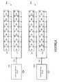
- FIG. 3depicted is a schematic diagram of an exemplary portion of the array of EEPROM bit cells connected according to an exemplary embodiment of the invention.
- the present inventionis has the MOSFET sources of at least two groups of bit cells isolated and selectably connectable.
- un-selected bit cellsare not part of a selected bit cell(s) write circuit. Since the sources of the un-selected bit cells are “floating” (disconnected) any capacitance contribution and/or leakage currents are minimal.
- the circuits used to isolate the un-selected bit cellshave parasitic capacitance and leakage currents, but are minimal compared to the capacitance and leakage currents of a plurality of bit cell MOSFETs.
- the bit cell source isolation circuitsare in series with the bit cells and thus further reduce any parasitic capacitance (capacitors in series have less capacitance than either capacitor). Any leakage currents would generally be governed by the leakage current of the source isolation circuits.
- a bit cell 200is selected for a write operation by applying a low logic level or common reference voltage to cell source enable line 328 d , memory cell gate 222 b is set to V SS . Then a short, e.g., 1-10 millisecond Vpp+ write pulse is applied. Simultaneously, a short 1-10 millisecond Vpp pulse is applied to row 1 select line 232 b .
- the un-selected bit cellshave their respective source enable lines 328 a , 328 b and 328 c floating and no longer tied to the selected source enable line 328 d . Thus there is substantially no loading of the Vpp+ pulse by these un-selected bit cells.
- Parasitic capacitance, C ds and C gs , and leakage currentsaffect the rise time and ultimate voltage level of the Vpp+ write pulse.
- the prior art circuit of FIG. 2has all of the source connections of the bit cells connected to a common node (ground) and are potentially active circuit elements.
- the parasitic capacitance and leakage currents of the entire array of bit cellsare part of the active circuit loading that the charge pump (not illustrated) and write logic (not illustrated) must overcome in order to reliably write to the selected bit cell 200 .
- Increasing the number of bit cells 200increases the circuit loading that the Vpp+ write pulse must overcome.
- FIG. 4illustrates a schematic block diagram of an exemplary embodiment of the invention.
- a plurality of bit cells 300are grouped into at least two bit cell blocks 400 a and 400 b .
- Common source drivers 402 a and 402 brespectively, select one of the bit cell blocks 400 a and 400 b during a write operation.
- the other bit cell blockremains unselected and thus does not substantially contribute to loading of the write pulse Vpp+.
- the common source drivers 402 a and 402 bmay be, e.g., MOSFET or CMOS transistors (not illustrated) connected between the common sources of the bit cells and V SS (power supply common).
- Vppmay be derived from Vpp+
Landscapes
- Engineering & Computer Science (AREA)
- Microelectronics & Electronic Packaging (AREA)
- Read Only Memory (AREA)
- Non-Volatile Memory (AREA)
Abstract
Description
| TABLE I | |||||
| Read | Write | Erase | Standby | ||
| Bit Line | ˜1.6 volts | Vpp | 0.0 volts | 0.0 volts |
| Row Select Gate | VDD | Vpp+ | Vpp+ | 0.0 volts |
| Memory Cell Gate | ˜1.1 volts | 0.00 volts | Vpp | 0.0 volts |
| Common Source | 0.0 volts | Float | 0.0 volts | 0.0 volts |
Claims (30)
Priority Applications (3)
| Application Number | Priority Date | Filing Date | Title |
|---|---|---|---|
| US09/799,328US6459616B1 (en) | 2001-03-05 | 2001-03-05 | Split common source on EEPROM array |
| PCT/US2002/006290WO2002071408A1 (en) | 2001-03-05 | 2002-03-05 | Split common source on eeprom array |
| TW091104046ATW533587B (en) | 2001-03-05 | 2002-03-05 | Split common source on EEPROM array |
Applications Claiming Priority (1)
| Application Number | Priority Date | Filing Date | Title |
|---|---|---|---|
| US09/799,328US6459616B1 (en) | 2001-03-05 | 2001-03-05 | Split common source on EEPROM array |
Publications (2)
| Publication Number | Publication Date |
|---|---|
| US6459616B1true US6459616B1 (en) | 2002-10-01 |
| US20020141239A1 US20020141239A1 (en) | 2002-10-03 |
Family
ID=25175601
Family Applications (1)
| Application Number | Title | Priority Date | Filing Date |
|---|---|---|---|
| US09/799,328Expired - LifetimeUS6459616B1 (en) | 2001-03-05 | 2001-03-05 | Split common source on EEPROM array |
Country Status (3)
| Country | Link |
|---|---|
| US (1) | US6459616B1 (en) |
| TW (1) | TW533587B (en) |
| WO (1) | WO2002071408A1 (en) |
Cited By (7)
| Publication number | Priority date | Publication date | Assignee | Title |
|---|---|---|---|---|
| US20030200380A1 (en)* | 1996-11-05 | 2003-10-23 | Lee Douglas J. | Latched address multi-chunk write to EEPROM |
| US20070189075A1 (en)* | 2005-11-23 | 2007-08-16 | Udo Ausserlechner | Memory Circuit, Drive Circuit For A Memory And Method For Writing Write Data Into A Memory |
| US20100064098A1 (en)* | 1991-07-26 | 2010-03-11 | Lofgren Karl M J | Device and Method for Controlling Solid-State Memory System |
| US8320191B2 (en) | 2007-08-30 | 2012-11-27 | Infineon Technologies Ag | Memory cell arrangement, method for controlling a memory cell, memory array and electronic device |
| US8923049B2 (en) | 2011-09-09 | 2014-12-30 | Aplus Flash Technology, Inc | 1T1b and 2T2b flash-based, data-oriented EEPROM design |
| US20150346742A1 (en)* | 2014-06-02 | 2015-12-03 | Nxp B.V. | Energy recycling for a cost effective platform to optimize energy efficiency for low powered system |
| US9536614B2 (en) | 2015-04-24 | 2017-01-03 | Nxp Usa, Inc. | Common source architecture for split gate memory |
Families Citing this family (1)
| Publication number | Priority date | Publication date | Assignee | Title |
|---|---|---|---|---|
| KR102313017B1 (en)* | 2015-08-21 | 2021-10-18 | 삼성전자주식회사 | Storage device comprising nonvolatile memory and controller controlling write of nonvolatile memory device and operating method of storage device |
Citations (3)
| Publication number | Priority date | Publication date | Assignee | Title |
|---|---|---|---|---|
| US6014328A (en)* | 1997-09-05 | 2000-01-11 | Mitsubishi Denki Kabushiki Kaisha | Memory cell allowing write and erase with low voltage power supply and nonvolatile semiconductor memory device provided with the same |
| US6091634A (en)* | 1997-04-11 | 2000-07-18 | Programmable Silicon Solutions | Compact nonvolatile memory using substrate hot carrier injection |
| US6195285B1 (en)* | 1997-09-09 | 2001-02-27 | Rohm Co., Ltd. | EEPROM device having a constant data writing duration |
Family Cites Families (5)
| Publication number | Priority date | Publication date | Assignee | Title |
|---|---|---|---|---|
| US4451905A (en)* | 1981-12-28 | 1984-05-29 | Hughes Aircraft Company | Electrically erasable programmable read-only memory cell having a single transistor |
| JP2688492B2 (en)* | 1987-06-19 | 1997-12-10 | アドバンスト・マイクロ・デバイシズ・インコーポレイテッド | Electrically erasable programmable read-only memory |
| US5912842A (en)* | 1995-11-14 | 1999-06-15 | Programmable Microelectronics Corp. | Nonvolatile PMOS two transistor memory cell and array |
| JP3378879B2 (en)* | 1997-12-10 | 2003-02-17 | 松下電器産業株式会社 | Nonvolatile semiconductor memory device and driving method thereof |
| US6114724A (en)* | 1998-03-31 | 2000-09-05 | Cypress Semiconductor Corporation | Nonvolatile semiconductor memory cell with select gate |
- 2001
- 2001-03-05USUS09/799,328patent/US6459616B1/ennot_activeExpired - Lifetime
- 2002
- 2002-03-05WOPCT/US2002/006290patent/WO2002071408A1/ennot_activeApplication Discontinuation
- 2002-03-05TWTW091104046Apatent/TW533587B/enactive
Patent Citations (3)
| Publication number | Priority date | Publication date | Assignee | Title |
|---|---|---|---|---|
| US6091634A (en)* | 1997-04-11 | 2000-07-18 | Programmable Silicon Solutions | Compact nonvolatile memory using substrate hot carrier injection |
| US6014328A (en)* | 1997-09-05 | 2000-01-11 | Mitsubishi Denki Kabushiki Kaisha | Memory cell allowing write and erase with low voltage power supply and nonvolatile semiconductor memory device provided with the same |
| US6195285B1 (en)* | 1997-09-09 | 2001-02-27 | Rohm Co., Ltd. | EEPROM device having a constant data writing duration |
Cited By (16)
| Publication number | Priority date | Publication date | Assignee | Title |
|---|---|---|---|---|
| US20100064098A1 (en)* | 1991-07-26 | 2010-03-11 | Lofgren Karl M J | Device and Method for Controlling Solid-State Memory System |
| US8125834B2 (en) | 1991-07-26 | 2012-02-28 | Sandisk Technologies Inc. | Device and method for controlling solid-state memory system |
| US7688643B2 (en) | 1991-07-26 | 2010-03-30 | Sandisk Corporation | Device and method for controlling solid-state memory system |
| US6829673B2 (en) | 1996-11-05 | 2004-12-07 | Sandisk Corporation | Latched address multi-chunk write to EEPROM |
| US7890694B2 (en) | 1996-11-05 | 2011-02-15 | Sandisk Corporation | Latched address multi-chunk write to EEPROM |
| US20030200380A1 (en)* | 1996-11-05 | 2003-10-23 | Lee Douglas J. | Latched address multi-chunk write to EEPROM |
| US20090228644A1 (en)* | 1996-11-05 | 2009-09-10 | Lee Douglas J | Latched Address Multi-Chunk Write to EEPROM |
| US20090073773A1 (en)* | 2005-11-23 | 2009-03-19 | Infineon Technologies Ag | Memory circuit, drive circuit for a memory and method for writing write data into a memory |
| US7599226B2 (en) | 2005-11-23 | 2009-10-06 | Infineon Technologies Ag | Memory circuit, drive circuit for a memory and method for writing write data into a memory |
| US7466596B2 (en) | 2005-11-23 | 2008-12-16 | Infineon Technologies Ag | Memory circuit, drive circuit for a memory and method for writing write data into a memory |
| US20070189075A1 (en)* | 2005-11-23 | 2007-08-16 | Udo Ausserlechner | Memory Circuit, Drive Circuit For A Memory And Method For Writing Write Data Into A Memory |
| US8320191B2 (en) | 2007-08-30 | 2012-11-27 | Infineon Technologies Ag | Memory cell arrangement, method for controlling a memory cell, memory array and electronic device |
| US9030877B2 (en) | 2007-08-30 | 2015-05-12 | Infineon Technologies Ag | Memory cell arrangement, method for controlling a memory cell, memory array and electronic device |
| US8923049B2 (en) | 2011-09-09 | 2014-12-30 | Aplus Flash Technology, Inc | 1T1b and 2T2b flash-based, data-oriented EEPROM design |
| US20150346742A1 (en)* | 2014-06-02 | 2015-12-03 | Nxp B.V. | Energy recycling for a cost effective platform to optimize energy efficiency for low powered system |
| US9536614B2 (en) | 2015-04-24 | 2017-01-03 | Nxp Usa, Inc. | Common source architecture for split gate memory |
Also Published As
| Publication number | Publication date |
|---|---|
| WO2002071408A1 (en) | 2002-09-12 |
| US20020141239A1 (en) | 2002-10-03 |
| TW533587B (en) | 2003-05-21 |
Similar Documents
| Publication | Publication Date | Title |
|---|---|---|
| US6141250A (en) | Non-volatile semiconductor memory device | |
| US6370062B2 (en) | NAND-type flash memory device and method of operating the same | |
| JP4966472B2 (en) | Electrically erasable programmable read-only memory with small page size write and erase | |
| KR0172441B1 (en) | Programming method of non-volatile semiconductor memory | |
| US8017994B2 (en) | Nonvolatile semiconductor memory | |
| US6269021B1 (en) | Memory cell of nonvolatile semiconductor memory device | |
| US7161833B2 (en) | Self-boosting system for flash memory cells | |
| KR100187196B1 (en) | Nonvolatile Semiconductor Memory Device | |
| KR100378273B1 (en) | Channel erased-type nonvolatile semiconductor memory device | |
| US7016229B2 (en) | Page buffer for NAND flash memory | |
| US6570787B1 (en) | Programming with floating source for low power, low leakage and high density flash memory devices | |
| US20020126532A1 (en) | Non-volatile semiconductor memory device | |
| USRE37311E1 (en) | Parallel type nonvolatile semiconductor memory device and method of using the same | |
| KR100858293B1 (en) | A data processing method of a NAD flash memory and a NAD flash memory including a NAD memory cell array and the NAD memory cell array | |
| US20060083072A1 (en) | Semiconductor memory device with MOS transistors each having floating gate and control gate | |
| KR20040068552A (en) | Semiconductor device having a byte-erasable eeprom memory | |
| WO1997022971A9 (en) | A negative voltage switch architecture for a nonvolatile memory | |
| KR100639827B1 (en) | 1 transistor cell for EEPROM applications | |
| US6459616B1 (en) | Split common source on EEPROM array | |
| US7164606B1 (en) | Reverse fowler-nordheim tunneling programming for non-volatile memory cell | |
| JP3908432B2 (en) | Nonvolatile semiconductor memory device and writing method thereof | |
| KR100254565B1 (en) | Row decoder circuit of flash memory device having divided word line structure | |
| US6646925B2 (en) | Method and system for discharging the bit lines of a memory cell array after erase operation | |
| US6418055B1 (en) | One-chip microcomputer | |
| US7038951B2 (en) | Non-volatile semiconductor memory device and erasing control method thereof |
Legal Events
| Date | Code | Title | Description |
|---|---|---|---|
| AS | Assignment | Owner name:MICROCHIP TECHNOLOGY INCORPORATED, ARIZONA Free format text:ASSIGNMENT OF ASSIGNORS INTEREST;ASSIGNORS:BEAUCHAMP, BRUCE;SALT, TOM;REEL/FRAME:011894/0413 Effective date:20010521 | |
| STCF | Information on status: patent grant | Free format text:PATENTED CASE | |
| FPAY | Fee payment | Year of fee payment:4 | |
| FPAY | Fee payment | Year of fee payment:8 | |
| FPAY | Fee payment | Year of fee payment:12 | |
| AS | Assignment | Owner name:JPMORGAN CHASE BANK, N.A., AS ADMINISTRATIVE AGENT, ILLINOIS Free format text:SECURITY INTEREST;ASSIGNOR:MICROCHIP TECHNOLOGY INCORPORATED;REEL/FRAME:041675/0617 Effective date:20170208 Owner name:JPMORGAN CHASE BANK, N.A., AS ADMINISTRATIVE AGENT Free format text:SECURITY INTEREST;ASSIGNOR:MICROCHIP TECHNOLOGY INCORPORATED;REEL/FRAME:041675/0617 Effective date:20170208 | |
| AS | Assignment | Owner name:JPMORGAN CHASE BANK, N.A., AS ADMINISTRATIVE AGENT, ILLINOIS Free format text:SECURITY INTEREST;ASSIGNORS:MICROCHIP TECHNOLOGY INCORPORATED;SILICON STORAGE TECHNOLOGY, INC.;ATMEL CORPORATION;AND OTHERS;REEL/FRAME:046426/0001 Effective date:20180529 Owner name:JPMORGAN CHASE BANK, N.A., AS ADMINISTRATIVE AGENT Free format text:SECURITY INTEREST;ASSIGNORS:MICROCHIP TECHNOLOGY INCORPORATED;SILICON STORAGE TECHNOLOGY, INC.;ATMEL CORPORATION;AND OTHERS;REEL/FRAME:046426/0001 Effective date:20180529 | |
| AS | Assignment | Owner name:WELLS FARGO BANK, NATIONAL ASSOCIATION, AS NOTES COLLATERAL AGENT, CALIFORNIA Free format text:SECURITY INTEREST;ASSIGNORS:MICROCHIP TECHNOLOGY INCORPORATED;SILICON STORAGE TECHNOLOGY, INC.;ATMEL CORPORATION;AND OTHERS;REEL/FRAME:047103/0206 Effective date:20180914 Owner name:WELLS FARGO BANK, NATIONAL ASSOCIATION, AS NOTES C Free format text:SECURITY INTEREST;ASSIGNORS:MICROCHIP TECHNOLOGY INCORPORATED;SILICON STORAGE TECHNOLOGY, INC.;ATMEL CORPORATION;AND OTHERS;REEL/FRAME:047103/0206 Effective date:20180914 | |
| AS | Assignment | Owner name:JPMORGAN CHASE BANK, N.A., AS ADMINISTRATIVE AGENT, DELAWARE Free format text:SECURITY INTEREST;ASSIGNORS:MICROCHIP TECHNOLOGY INC.;SILICON STORAGE TECHNOLOGY, INC.;ATMEL CORPORATION;AND OTHERS;REEL/FRAME:053311/0305 Effective date:20200327 | |
| AS | Assignment | Owner name:MICROCHIP TECHNOLOGY INC., ARIZONA Free format text:RELEASE BY SECURED PARTY;ASSIGNOR:JPMORGAN CHASE BANK, N.A, AS ADMINISTRATIVE AGENT;REEL/FRAME:053466/0011 Effective date:20200529 Owner name:ATMEL CORPORATION, ARIZONA Free format text:RELEASE BY SECURED PARTY;ASSIGNOR:JPMORGAN CHASE BANK, N.A, AS ADMINISTRATIVE AGENT;REEL/FRAME:053466/0011 Effective date:20200529 Owner name:SILICON STORAGE TECHNOLOGY, INC., ARIZONA Free format text:RELEASE BY SECURED PARTY;ASSIGNOR:JPMORGAN CHASE BANK, N.A, AS ADMINISTRATIVE AGENT;REEL/FRAME:053466/0011 Effective date:20200529 Owner name:MICROSEMI STORAGE SOLUTIONS, INC., ARIZONA Free format text:RELEASE BY SECURED PARTY;ASSIGNOR:JPMORGAN CHASE BANK, N.A, AS ADMINISTRATIVE AGENT;REEL/FRAME:053466/0011 Effective date:20200529 Owner name:MICROSEMI CORPORATION, CALIFORNIA Free format text:RELEASE BY SECURED PARTY;ASSIGNOR:JPMORGAN CHASE BANK, N.A, AS ADMINISTRATIVE AGENT;REEL/FRAME:053466/0011 Effective date:20200529 | |
| AS | Assignment | Owner name:WELLS FARGO BANK, NATIONAL ASSOCIATION, MINNESOTA Free format text:SECURITY INTEREST;ASSIGNORS:MICROCHIP TECHNOLOGY INC.;SILICON STORAGE TECHNOLOGY, INC.;ATMEL CORPORATION;AND OTHERS;REEL/FRAME:053468/0705 Effective date:20200529 | |
| AS | Assignment | Owner name:WELLS FARGO BANK, NATIONAL ASSOCIATION, AS COLLATERAL AGENT, MINNESOTA Free format text:SECURITY INTEREST;ASSIGNORS:MICROCHIP TECHNOLOGY INCORPORATED;SILICON STORAGE TECHNOLOGY, INC.;ATMEL CORPORATION;AND OTHERS;REEL/FRAME:055671/0612 Effective date:20201217 | |
| AS | Assignment | Owner name:MICROSEMI STORAGE SOLUTIONS, INC., ARIZONA Free format text:RELEASE BY SECURED PARTY;ASSIGNOR:JPMORGAN CHASE BANK, N.A., AS ADMINISTRATIVE AGENT;REEL/FRAME:059333/0222 Effective date:20220218 Owner name:MICROSEMI CORPORATION, ARIZONA Free format text:RELEASE BY SECURED PARTY;ASSIGNOR:JPMORGAN CHASE BANK, N.A., AS ADMINISTRATIVE AGENT;REEL/FRAME:059333/0222 Effective date:20220218 Owner name:ATMEL CORPORATION, ARIZONA Free format text:RELEASE BY SECURED PARTY;ASSIGNOR:JPMORGAN CHASE BANK, N.A., AS ADMINISTRATIVE AGENT;REEL/FRAME:059333/0222 Effective date:20220218 Owner name:SILICON STORAGE TECHNOLOGY, INC., ARIZONA Free format text:RELEASE BY SECURED PARTY;ASSIGNOR:JPMORGAN CHASE BANK, N.A., AS ADMINISTRATIVE AGENT;REEL/FRAME:059333/0222 Effective date:20220218 Owner name:MICROCHIP TECHNOLOGY INCORPORATED, ARIZONA Free format text:RELEASE BY SECURED PARTY;ASSIGNOR:JPMORGAN CHASE BANK, N.A., AS ADMINISTRATIVE AGENT;REEL/FRAME:059333/0222 Effective date:20220218 | |
| AS | Assignment | Owner name:MICROCHIP TECHNOLOGY INCORPORATED, ARIZONA Free format text:RELEASE BY SECURED PARTY;ASSIGNOR:JPMORGAN CHASE BANK, N.A., AS ADMINISTRATIVE AGENT;REEL/FRAME:059666/0545 Effective date:20220218 | |
| AS | Assignment | Owner name:MICROSEMI STORAGE SOLUTIONS, INC., ARIZONA Free format text:RELEASE BY SECURED PARTY;ASSIGNOR:WELLS FARGO BANK, NATIONAL ASSOCIATION, AS NOTES COLLATERAL AGENT;REEL/FRAME:059358/0001 Effective date:20220228 Owner name:MICROSEMI CORPORATION, ARIZONA Free format text:RELEASE BY SECURED PARTY;ASSIGNOR:WELLS FARGO BANK, NATIONAL ASSOCIATION, AS NOTES COLLATERAL AGENT;REEL/FRAME:059358/0001 Effective date:20220228 Owner name:ATMEL CORPORATION, ARIZONA Free format text:RELEASE BY SECURED PARTY;ASSIGNOR:WELLS FARGO BANK, NATIONAL ASSOCIATION, AS NOTES COLLATERAL AGENT;REEL/FRAME:059358/0001 Effective date:20220228 Owner name:SILICON STORAGE TECHNOLOGY, INC., ARIZONA Free format text:RELEASE BY SECURED PARTY;ASSIGNOR:WELLS FARGO BANK, NATIONAL ASSOCIATION, AS NOTES COLLATERAL AGENT;REEL/FRAME:059358/0001 Effective date:20220228 Owner name:MICROCHIP TECHNOLOGY INCORPORATED, ARIZONA Free format text:RELEASE BY SECURED PARTY;ASSIGNOR:WELLS FARGO BANK, NATIONAL ASSOCIATION, AS NOTES COLLATERAL AGENT;REEL/FRAME:059358/0001 Effective date:20220228 | |
| AS | Assignment | Owner name:MICROSEMI STORAGE SOLUTIONS, INC., ARIZONA Free format text:RELEASE BY SECURED PARTY;ASSIGNOR:WELLS FARGO BANK, NATIONAL ASSOCIATION, AS NOTES COLLATERAL AGENT;REEL/FRAME:059863/0400 Effective date:20220228 Owner name:MICROSEMI CORPORATION, ARIZONA Free format text:RELEASE BY SECURED PARTY;ASSIGNOR:WELLS FARGO BANK, NATIONAL ASSOCIATION, AS NOTES COLLATERAL AGENT;REEL/FRAME:059863/0400 Effective date:20220228 Owner name:ATMEL CORPORATION, ARIZONA Free format text:RELEASE BY SECURED PARTY;ASSIGNOR:WELLS FARGO BANK, NATIONAL ASSOCIATION, AS NOTES COLLATERAL AGENT;REEL/FRAME:059863/0400 Effective date:20220228 Owner name:SILICON STORAGE TECHNOLOGY, INC., ARIZONA Free format text:RELEASE BY SECURED PARTY;ASSIGNOR:WELLS FARGO BANK, NATIONAL ASSOCIATION, AS NOTES COLLATERAL AGENT;REEL/FRAME:059863/0400 Effective date:20220228 Owner name:MICROCHIP TECHNOLOGY INCORPORATED, ARIZONA Free format text:RELEASE BY SECURED PARTY;ASSIGNOR:WELLS FARGO BANK, NATIONAL ASSOCIATION, AS NOTES COLLATERAL AGENT;REEL/FRAME:059863/0400 Effective date:20220228 | |
| AS | Assignment | Owner name:MICROSEMI STORAGE SOLUTIONS, INC., ARIZONA Free format text:RELEASE BY SECURED PARTY;ASSIGNOR:WELLS FARGO BANK, NATIONAL ASSOCIATION, AS NOTES COLLATERAL AGENT;REEL/FRAME:059363/0001 Effective date:20220228 Owner name:MICROSEMI CORPORATION, ARIZONA Free format text:RELEASE BY SECURED PARTY;ASSIGNOR:WELLS FARGO BANK, NATIONAL ASSOCIATION, AS NOTES COLLATERAL AGENT;REEL/FRAME:059363/0001 Effective date:20220228 Owner name:ATMEL CORPORATION, ARIZONA Free format text:RELEASE BY SECURED PARTY;ASSIGNOR:WELLS FARGO BANK, NATIONAL ASSOCIATION, AS NOTES COLLATERAL AGENT;REEL/FRAME:059363/0001 Effective date:20220228 Owner name:SILICON STORAGE TECHNOLOGY, INC., ARIZONA Free format text:RELEASE BY SECURED PARTY;ASSIGNOR:WELLS FARGO BANK, NATIONAL ASSOCIATION, AS NOTES COLLATERAL AGENT;REEL/FRAME:059363/0001 Effective date:20220228 Owner name:MICROCHIP TECHNOLOGY INCORPORATED, ARIZONA Free format text:RELEASE BY SECURED PARTY;ASSIGNOR:WELLS FARGO BANK, NATIONAL ASSOCIATION, AS NOTES COLLATERAL AGENT;REEL/FRAME:059363/0001 Effective date:20220228 | |
| AS | Assignment | Owner name:MICROSEMI STORAGE SOLUTIONS, INC., ARIZONA Free format text:RELEASE BY SECURED PARTY;ASSIGNOR:WELLS FARGO BANK, NATIONAL ASSOCIATION, AS NOTES COLLATERAL AGENT;REEL/FRAME:060894/0437 Effective date:20220228 Owner name:MICROSEMI CORPORATION, ARIZONA Free format text:RELEASE BY SECURED PARTY;ASSIGNOR:WELLS FARGO BANK, NATIONAL ASSOCIATION, AS NOTES COLLATERAL AGENT;REEL/FRAME:060894/0437 Effective date:20220228 Owner name:ATMEL CORPORATION, ARIZONA Free format text:RELEASE BY SECURED PARTY;ASSIGNOR:WELLS FARGO BANK, NATIONAL ASSOCIATION, AS NOTES COLLATERAL AGENT;REEL/FRAME:060894/0437 Effective date:20220228 Owner name:SILICON STORAGE TECHNOLOGY, INC., ARIZONA Free format text:RELEASE BY SECURED PARTY;ASSIGNOR:WELLS FARGO BANK, NATIONAL ASSOCIATION, AS NOTES COLLATERAL AGENT;REEL/FRAME:060894/0437 Effective date:20220228 Owner name:MICROCHIP TECHNOLOGY INCORPORATED, ARIZONA Free format text:RELEASE BY SECURED PARTY;ASSIGNOR:WELLS FARGO BANK, NATIONAL ASSOCIATION, AS NOTES COLLATERAL AGENT;REEL/FRAME:060894/0437 Effective date:20220228 |