US6458656B1 - Process for creating a flash memory cell using a photoresist flow operation - Google Patents
Process for creating a flash memory cell using a photoresist flow operationDownload PDFInfo
- Publication number
- US6458656B1 US6458656B1US09/628,130US62813000AUS6458656B1US 6458656 B1US6458656 B1US 6458656B1US 62813000 AUS62813000 AUS 62813000AUS 6458656 B1US6458656 B1US 6458656B1
- Authority
- US
- United States
- Prior art keywords
- semiconductor substrate
- resist mask
- type dopant
- resist
- overlying
- Prior art date
- Legal status (The legal status is an assumption and is not a legal conclusion. Google has not performed a legal analysis and makes no representation as to the accuracy of the status listed.)
- Expired - Lifetime, expires
Links
- 238000000034methodMethods0.000titleclaimsabstractdescription32
- 230000008569processEffects0.000titleclaimsabstractdescription27
- 229920002120photoresistant polymerPolymers0.000titledescription16
- 239000000758substrateSubstances0.000claimsabstractdescription117
- 239000004065semiconductorSubstances0.000claimsabstractdescription116
- 239000002019doping agentSubstances0.000claimsabstractdescription48
- 239000007943implantSubstances0.000claimsabstractdescription43
- 238000000059patterningMethods0.000claimsabstractdescription6
- 238000000151depositionMethods0.000claimsabstractdescription4
- VYPSYNLAJGMNEJ-UHFFFAOYSA-NSilicium dioxideChemical compoundO=[Si]=OVYPSYNLAJGMNEJ-UHFFFAOYSA-N0.000claimsdescription50
- 229910052581Si3N4Inorganic materials0.000claimsdescription25
- 235000012239silicon dioxideNutrition0.000claimsdescription25
- 239000000377silicon dioxideSubstances0.000claimsdescription25
- HQVNEWCFYHHQES-UHFFFAOYSA-Nsilicon nitrideChemical compoundN12[Si]34N5[Si]62N3[Si]51N64HQVNEWCFYHHQES-UHFFFAOYSA-N0.000claimsdescription25
- 230000001154acute effectEffects0.000claimsdescription6
- 238000005530etchingMethods0.000claims3
- 238000004519manufacturing processMethods0.000description13
- 238000005468ion implantationMethods0.000description8
- 229910052785arsenicInorganic materials0.000description6
- RQNWIZPPADIBDY-UHFFFAOYSA-Narsenic atomChemical compound[As]RQNWIZPPADIBDY-UHFFFAOYSA-N0.000description6
- ZOXJGFHDIHLPTG-UHFFFAOYSA-NBoronChemical compound[B]ZOXJGFHDIHLPTG-UHFFFAOYSA-N0.000description4
- 229910052796boronInorganic materials0.000description4
- 230000008901benefitEffects0.000description3
- 238000005516engineering processMethods0.000description3
- 239000000463materialSubstances0.000description3
- BLRPTPMANUNPDV-UHFFFAOYSA-NSilaneChemical compound[SiH4]BLRPTPMANUNPDV-UHFFFAOYSA-N0.000description2
- 238000004891communicationMethods0.000description2
- 238000011161developmentMethods0.000description2
- 239000003989dielectric materialSubstances0.000description2
- 230000005684electric fieldEffects0.000description2
- 230000014759maintenance of locationEffects0.000description2
- 238000012986modificationMethods0.000description2
- 230000004048modificationEffects0.000description2
- 230000027756respiratory electron transport chainEffects0.000description2
- XPDWGBQVDMORPB-UHFFFAOYSA-NFluoroformChemical compoundFC(F)FXPDWGBQVDMORPB-UHFFFAOYSA-N0.000description1
- 230000005689Fowler Nordheim tunnelingEffects0.000description1
- OAICVXFJPJFONN-UHFFFAOYSA-NPhosphorusChemical compound[P]OAICVXFJPJFONN-UHFFFAOYSA-N0.000description1
- 238000012356Product developmentMethods0.000description1
- XKMRRTOUMJRJIA-UHFFFAOYSA-Nammonia nh3Chemical compoundN.NXKMRRTOUMJRJIA-UHFFFAOYSA-N0.000description1
- 229910052787antimonyInorganic materials0.000description1
- WATWJIUSRGPENY-UHFFFAOYSA-Nantimony atomChemical compound[Sb]WATWJIUSRGPENY-UHFFFAOYSA-N0.000description1
- 238000003491arrayMethods0.000description1
- 230000015572biosynthetic processEffects0.000description1
- 230000015556catabolic processEffects0.000description1
- 238000013500data storageMethods0.000description1
- 230000007423decreaseEffects0.000description1
- 238000011982device technologyMethods0.000description1
- MROCJMGDEKINLD-UHFFFAOYSA-NdichlorosilaneChemical compoundCl[SiH2]ClMROCJMGDEKINLD-UHFFFAOYSA-N0.000description1
- 239000002784hot electronSubstances0.000description1
- 238000002347injectionMethods0.000description1
- 239000007924injectionSubstances0.000description1
- 230000007246mechanismEffects0.000description1
- 229910021421monocrystalline siliconInorganic materials0.000description1
- 230000003647oxidationEffects0.000description1
- 238000007254oxidation reactionMethods0.000description1
- 229910052698phosphorusInorganic materials0.000description1
- 239000011574phosphorusSubstances0.000description1
- 238000005036potential barrierMethods0.000description1
- 238000012545processingMethods0.000description1
- 238000011160researchMethods0.000description1
- 238000000926separation methodMethods0.000description1
- 229910000077silaneInorganic materials0.000description1
- 238000003860storageMethods0.000description1
- 238000012546transferMethods0.000description1
Images


Classifications
- H—ELECTRICITY
- H10—SEMICONDUCTOR DEVICES; ELECTRIC SOLID-STATE DEVICES NOT OTHERWISE PROVIDED FOR
- H10B—ELECTRONIC MEMORY DEVICES
- H10B43/00—EEPROM devices comprising charge-trapping gate insulators
- H10B43/30—EEPROM devices comprising charge-trapping gate insulators characterised by the memory core region
- H—ELECTRICITY
- H10—SEMICONDUCTOR DEVICES; ELECTRIC SOLID-STATE DEVICES NOT OTHERWISE PROVIDED FOR
- H10B—ELECTRONIC MEMORY DEVICES
- H10B69/00—Erasable-and-programmable ROM [EPROM] devices not provided for in groups H10B41/00 - H10B63/00, e.g. ultraviolet erasable-and-programmable ROM [UVEPROM] devices
- H—ELECTRICITY
- H10—SEMICONDUCTOR DEVICES; ELECTRIC SOLID-STATE DEVICES NOT OTHERWISE PROVIDED FOR
- H10D—INORGANIC ELECTRIC SEMICONDUCTOR DEVICES
- H10D30/00—Field-effect transistors [FET]
- H10D30/01—Manufacture or treatment
- H10D30/021—Manufacture or treatment of FETs having insulated gates [IGFET]
- H10D30/0413—Manufacture or treatment of FETs having insulated gates [IGFET] of FETs having charge-trapping gate insulators, e.g. MNOS transistors
- Y—GENERAL TAGGING OF NEW TECHNOLOGICAL DEVELOPMENTS; GENERAL TAGGING OF CROSS-SECTIONAL TECHNOLOGIES SPANNING OVER SEVERAL SECTIONS OF THE IPC; TECHNICAL SUBJECTS COVERED BY FORMER USPC CROSS-REFERENCE ART COLLECTIONS [XRACs] AND DIGESTS
- Y10—TECHNICAL SUBJECTS COVERED BY FORMER USPC
- Y10S—TECHNICAL SUBJECTS COVERED BY FORMER USPC CROSS-REFERENCE ART COLLECTIONS [XRACs] AND DIGESTS
- Y10S438/00—Semiconductor device manufacturing: process
- Y10S438/954—Making oxide-nitride-oxide device
Definitions
- This inventionrelates generally to non-volatile memory devices.
- the present inventionrelates to a method and process for manufacturing a non-volatile memory device.
- Non-volatile memory devicesare currently in widespread use in electronic components that require the retention of information when electrical power is terminated.
- Non-volatile memory devicesinclude read-only-memory (ROM), programmable-read-only memory (PROM), erasable-programmable-read-only memory (EPROM), and electrically-erasable-programmable-read-only-memory (EEPROM) devices.
- EEPROM devicesdiffer from other non-volatile memory devices in that they can be electrically programmed and erased.
- Flash EEPROM devicesare similar to EEPROM devices in that memory cells can be programmed and erased electrically. However, Flash EEPROM devices enable the erasing of all memory cells in the device using a single electrical current pulse.
- an EEPROM devicetypically includes a floating-gate electrode upon which electrical charge is stored.
- the floating-gate electrodeoverlies a channel region residing between source and drain regions in a semiconductor substrate.
- the floating-gate electrodetogether with the source and drain regions forms an enhancement transistor.
- the threshold voltage of the enhancement transistoris brought to a relatively high value.
- the threshold voltage of the enhancement transistoris brought to a relatively low value.
- the threshold level of the enhancement transistordetermines the current flow through the transistor when the transistor is turned on by the application of appropriate voltages to the gate and drain. When the threshold voltage is high, no current will flow through the transistor, which is defined as a logic 0 state.
- a flash EEPROM deviceelectrons are transferred to a floating-gate electrode through a dielectric layer overlying the channel region of the enhancement transistor.
- the electron transferis initiated by either hot electron injection, or by Fowler-Nordheim tunneling.
- a voltage potentialis applied to the floating-gate by an overlying control-gate electrode.
- the control-gate electrodeis capacitively coupled to the floating-gate electrode, such that a voltage applied on the control-gate electrode is coupled to the floating-gateelectrode.
- the flash EEPROM deviceis programmed by applying a high positive voltage to the control-gate electrode, and a lower positive voltage to the drain region, which transfers electrons from the channel region to the floating-gate electrode.
- the flash EEPROM deviceis erased by grounding the control-gate electrode and applying a high positive voltage through either the source or drain region of the enhancement transistor. Under erase voltage conditions, electrons are removed from the floating-gate electrode and transferred into either the source or drain regions in the semiconductor substrate.
- oxide-nitride-oxide (ONO) layerOne important dielectric material for the fabrication of the floating-gate electrode is an oxide-nitride-oxide (ONO) layer.
- ONOoxide-nitride-oxide
- During programmingelectrical charge is transferred from the substrate to the silicon nitride layer in the ONO layer. Voltages are applied to the gate and drain creating vertical and lateral electric fields, which accelerate the electrons along the length of the channel. As the electrons move along the channel, some of them gain sufficient energy to jump over the potential barrier of the bottom silicon dioxide layer and become trapped in the silicon nitride layer. Electrons are trapped near the drain region because the electric fields are the strongest near the drain. Reversing the potentials applied to the source and drain will cause electrons to travel along the channel in the opposite direction and be injected into the silicon nitride layer near the source region.
- ONOoxide-nitride-oxide
- silicon nitrideis not electrically conductive, the charge introduced into the silicon nitride layer tends to remain localized. Accordingly, depending upon the application of voltage potentials, electrical charge can be stored in regions within a single continuous silicon nitride layer.
- Non-volatile memory designershave taken advantage of the localized nature of electron storage within a silicon nitride layer and have designed memory devices that utilize two regions of stored charge within an ONO layer.
- This type of non-volatile memory deviceis known as a two-bit EEPROM.
- the two-bit EEPROMis capable of storing twice as much information as a conventional EEPROM in a memory array of equal size.
- a left and right bitis stored in physically different areas of the silicon nitride layer, near left and right regions of each memory cell. Programming methods are then used that enable two-bits to be programmed and read simultaneously.
- the two-bits of the memory cellcan be individually erased by applying suitable erase voltages to the gate and to either the source or drain regions.
- an ONO layeris formed having a first silicon dioxide layer overlying the semiconductor substrate, a silicon nitride layer overlying the first silicon dioxide layer, and a second silicon dioxide layer overlying the silicon nitride layer. A layer of photo resist is then spun on the ONO layer.
- the photoresistis patterned into a resist mask and the semiconductor substrate is doped with a p-type dopant such as boron using ion implantation at a large angle of incidence relative to the principal surface of the semiconductor substrate to allow the p-type implant to be located away from a subsequent n-type dopant.
- the waferis then rotated 180° and the semiconductor substrate is doped a second time with a p-type dopant using ion implantation at a large angle of incidence relative to the principal surface of the semiconductor substrate. Doping the semiconductor substrate with a p-type dopant creates p-type regions.
- the semiconductor substrateis then doped with an n-type dopant such as arsenic using ion implantation at an angle substantially normal to the principal surface of the semiconductor substrate. Doping the semiconductor substrate with n-type dopants creates n-type regions. Typically, the ONO layer is etched before the semiconductor substrate is doped with n-type dopants in order to make the implant of n-type dopants a more controlled implant. Once the n-type dopants have been implanted in the semiconductor substrate, the resist mask is stripped and cleaned from the ONO layer and a bit-line oxide region is thermally grown onto the semiconductor substrate.
- an n-type dopantsuch as arsenic using ion implantation at an angle substantially normal to the principal surface of the semiconductor substrate. Doping the semiconductor substrate with n-type dopants creates n-type regions. Typically, the ONO layer is etched before the semiconductor substrate is doped with n-type dopants in order to make the implant of n-type dopants a
- the resist maskhas to meet two conflicting requirements: the resist mask has to be thin enough to accommodate the large angle of incidence of the p-type implant, and yet the resist mask has to be thick enough to withstand the n-type implant. If the resist mask is too thick, the p-type implant must be made with a smaller angle of incidence, however if the resist mask is too thin the n-type implant cannot be made at all because the resist mask would have been too heavily degraded. Accordingly, advances in memory cell fabrication technology are necessary to insure patterning of high density memory cells used in two-bit EEPROM devices.
- the present inventionis for a process for fabricating a memory cell in a non-volatile memory device, preferably in a two-bit EEPROM device.
- Fabrication of a two-bit EEPROM device having a memory cellrequires the formation of p-type regions and n-type regions with good critical dimension control. This is because proper functionality of the two-bit EEPROM device during a programming operation requires voltages to be applied to the p-type regions and n-type regions.
- the p-type regionsmust be positioned at the edges of the ONO layer for fabrication of high density devices.
- fabrication of high density devices with p-type regions positioned at the edges of the ONO layeris hard to obtain due to the limitations of the resist mask.
- a process for fabricating a memory cellincludes providing a semiconductor substrate and forming an ONO layer over the semiconductor substrate. A layer of photoresist is then deposited overlying the ONO layer and patterned into a resist mask. The resist mask is thick enough to withstand an n-type implant.
- the ONO layeris etched before the semiconductor substrate is doped with n-type dopants in order to make the implant of n-type dopants a more controlled implant, however, the ONO layer may be etched after the semiconductor substrate is doped with n-type dopants.
- the semiconductor substrateis then doped with an n-type dopant such as arsenic, preferably by using ion implantation.
- the doping of the semiconductor substrate with an n-type dopantcauses n-type regions to form in the semiconductor substrate.
- the n-type implantis a direct implant, which is an implant at an angle substantially normal with respect to the principal surface of the semiconductor surface.
- a resist flow operationis performed on the semiconductor substrate by placing the semiconductor substrate in an oven.
- the resist flow operationthins down the resist mask and causes the corners of the resist mask to become rounded.
- the semiconductor substrateis doped with p-type dopants such as boron, preferably by using ion implantation.
- the p-type implantis an angled implant, which is an implant at an angle substantially acute with respect to the principal surface of the semiconductor substrate.
- the doping of the semiconductor substrate with p-type dopantscauses p-type regions to form in the semiconductor substrate.
- the resist maskis removed and the bit-line oxide region is formed.
- the rounded corners and thinness of the resist maskallow for a more angled p-type implant.
- the more angled p-type implantallows for the fabrication of a memory cell having p-type regions positioned at the edges of the ONO layer.
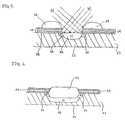
- FIG. 1illustrates, in cross-section, a portion of a memory cell containing p-type regions, in accordance with one preferred embodiment of the invention
- FIGS. 2-6illustrate, in cross-section, process steps for the fabrication of a memory cell, in accordance with one preferred embodiment of the invention.
- FIG. 1Shown in FIG. 1, in cross-section, is memory cell 20 suitable for use in a two-bit EEPROM device.
- memory cell 20suitable for use in a two-bit EEPROM device.
- FIGS. 1-6illustrate only one memory cell 20
- a two-bit EEPROM devicemay have many more memory cells identical to memory cell 20 .
- these additional memory cellshave been left out of FIGS. 1-6.
- Memory cell 20includes p-type regions 44 and n-type regions 46 located in semiconductor substrate 22 and separated by channel region 23 , as illustrated in FIG. 1 .
- Bit-line oxide region 50overlies p-type regions 44 and n-type regions 46 , respectively.
- Oxide-nitride-oxide (ONO) layer 24includes first silicon dioxide layer 26 overlying channel region 23 .
- Silicon nitride layer 28overlies first silicon dioxide layer 26 .
- Second silicon dioxide layer 30overlies silicon nitride layer 28 .
- dataresides in a certain logic state on memory cell 20 .
- selected data from a selected memory cell 20can be output to an external communication unit by using n-type regions 46 .
- p-type regions 44 and n-type regions 46must be formed with great accuracy.
- the resist maskhas to be thin enough to accommodate the large angle of incidence of the p-type implant, and yet the resist mask has to be thick enough to withstand the n-type implant.
- ONO layer 24is formed overlying the surface of semiconductor substrate 22 .
- semiconductor substrate 22is a single crystal silicon substrate.
- Semiconductor substrate 22has principal surface 38 previously processed and cleaned to remove debris and native oxides.
- ONO layer 24comprises first silicon dioxide layer 26 , silicon nitride layer 28 , and second silicon dioxide layer 30 .
- First silicon dioxide layer 26is formed overlying the semiconductor substrate 22 .
- first silicon dioxide layer 26has a thickness of about 50 to about 150 angstroms and, more preferably, a thickness of about 80 angstroms.
- silicon nitride layer 28is deposited overlying first silicon dioxide layer 26 , as illustrated in FIG. 2 .
- silicon nitride layer 28is formed by reacting ammonia NH 3 with either dichlorosilane (SiCl 2 H 2 ) or silane (SiH 4 ).
- silicon nitride layer 28is deposited overlying first silicon dioxide layer 26 having an initial thickness of about 120 to about 150 angstroms and, more preferably, an initial thickness of about 135 angstroms.
- second silicon dioxide layer 30is formed overlying silicon nitride layer 28 , as illustrated in FIG. 2 .
- silicon nitride layer 28decreases in thickness to a final thickness of about 50 to about 80 angstroms and, more preferably, a final thickness of about 60 angstroms.
- second silicon dioxide layer 30has a thickness of about 50 to about 150 angstroms and, more preferably, a thickness of about 80-95 angstroms.
- photoresist layer 36is deposited overlying ONO layer 24 .
- Photoresist layer 36 , and resist mask 34comprise any material known to one of ordinary skill in the art that can be used as a photoresist.
- photoresist layer 36 and resist mask 34comprise UV5 photoresist manufactured by Tokyo Electron specifically for 0.25 micron process technology.
- Photoresist layer 36must be thick enough to withstand the doping of semiconductor substrate 22 with n-type dopants.
- photoresist layer 36has a thickness of about 0.50 microns to about 2.0 microns and, more preferably, a thickness of about 1.0 microns.
- photoresist layer 36is patterned into resist mask 34 , as illustrated in FIG. 3 .
- photoresist layer 36is exposed to a light source, such as an x-ray source, which allows for the patterning of photoresist layer 36 into resist mask 34 .
- semiconductor substrate 22is then doped with an n-type dopant using resist mask 34 as a doping mask.
- n-type dopantcomprises an element selected from the group consisting of antimony, arsenic, and phosphorus.
- semiconductor substrate 22is doped with arsenic.
- the semiconductor substrate 22is doped with an n-type dopant, such as arsenic, by using ion implantation. Ion implantation allows for the fabrication of memory cell 20 with higher density and smaller feature sizes.
- resist mask 34as an ion implant mask, n-type implant 60 is then performed, as illustrated in FIG. 3 .
- the n-type implant 60is preferably arsenic implanted at a dose of about 1 ⁇ 10 14 cm ⁇ 2 to about 1 ⁇ 10 16 cm ⁇ 2 at an implant energy of about 20 KeV to about 80 KeV.
- n-type implant 60is performed through ONO layer 24 , but is masked out by resist mask 34 .
- the n-type implantis preferably a direct implant performed at an angle substantially normal to the principal surface 38 of the semiconductor substrate 22 , such as about a 90° angle, as illustrated in FIG. 3 .
- the n-type implant 60provides a high breakdown voltage for the drain node, which is needed during cell erasure.
- the n-type implant 60also forms the buried bit-line, which is a sub-surface conductive channel that carries a signal to each bit in the memory cell 20 .
- ONO layer 24is etched to expose part of the semiconductor substrate 22 before semiconductor substrate 22 is doped with n-type dopants in order to make n-type implant 60 a more controlled implant, as illustrated in FIG. 3 .
- ONO layeris etched before semiconductor substrate 22 is doped with n-type dopants, however ONO layer may be etched after semiconductor substrate 22 is doped with n-type dopants.
- a blanket anisotropic etchis performed to expose part of the semiconductor substrate 22 , as illustrated in FIG. 3 .
- the blanket anisotropic etchis performed using an etch comprising a gas selected from the group consisting of CF 4 and CHF 3 .
- a resist flow operationis performed on semiconductor substrate 22 by baking semiconductor substrate 22 in an oven.
- the resist flow operationthins down resist mask 34 and causes the corners of resist mask 34 to become rounded, as illustrated in FIG. 4 .
- the resist flow operationcan be performed in any oven known to one of ordinary skill in the art, such as an RTA furnace and a tunnel oven.
- semiconductor substrate 22is baked in a tunnel oven at a temperature of between about 100° C. to about 300° C. for about 5 minutes to about 30 minutes, and more preferably about 200° C. for about 10 minutes.
- semiconductor substrate 22is baked in an RTA furnace at a temperature of between about 100° C. to about 300° C. for about 10 seconds to about 1 minute.
- semiconductor substrate 22is doped with a p-type dopant, as illustrated in FIG. 5 .
- semiconductor substrate 22is doped with a p-type dopant by using ion implantation.
- the p-type dopantcomprises boron.
- p-type implant 62is performed to fix the threshold voltage of the select transistor, as illustrated in FIG. 5 .
- the p-type implant 62is preferably boron implanted at a dose of about 1 ⁇ 10 12 cm ⁇ 2 to about 1 ⁇ 10 14 cm ⁇ 2 at an implant energy of about 20 KeV to about 80 KeV.
- the p-type implant 62is performed directly onto semiconductor substrate 22 , but is masked out by resist mask 34 , as illustrated in FIG. 5 .
- the p-type implant 62is an angled implant, that is, an implant at an angle acute with respect to the principal surface of the semiconductor substrate. If a resist flow operation is performed on semiconductor substrate 22 to thin down resist mask 34 and cause the edges of resist mask 34 to become rounded, p-type implant 62 can be performed at an angle substantially acute with respect to the principal surface of the semiconductor substrate 22 , such as at an angle of about 7° to about 60° with respect to the principal surface of the semiconductor substrate 22 , and more preferably at an angle of about 30° with respect to the principal surface of the semiconductor substrate 22 .
- bit-line oxide region 50is formed overlying the exposed semiconductor substrate 22 , as illustrated in FIG. 6 .
- bit-line oxide region 50is formed by thermally growing a layer of silicon dioxide into and on top of the exposed semiconductor substrate 22 , however bit-line oxide region 50 can be formed by any one of a number of methods for growing oxide known to one of ordinary skill in the art, such as high-pressure oxidation, or rapid thermal processing.
Landscapes
- Semiconductor Memories (AREA)
- Non-Volatile Memory (AREA)
Abstract
Description
Claims (17)
Priority Applications (1)
| Application Number | Priority Date | Filing Date | Title |
|---|---|---|---|
| US09/628,130US6458656B1 (en) | 2000-03-16 | 2000-07-28 | Process for creating a flash memory cell using a photoresist flow operation |
Applications Claiming Priority (2)
| Application Number | Priority Date | Filing Date | Title |
|---|---|---|---|
| US18980300P | 2000-03-16 | 2000-03-16 | |
| US09/628,130US6458656B1 (en) | 2000-03-16 | 2000-07-28 | Process for creating a flash memory cell using a photoresist flow operation |
Publications (1)
| Publication Number | Publication Date |
|---|---|
| US6458656B1true US6458656B1 (en) | 2002-10-01 |
Family
ID=26885516
Family Applications (1)
| Application Number | Title | Priority Date | Filing Date |
|---|---|---|---|
| US09/628,130Expired - LifetimeUS6458656B1 (en) | 2000-03-16 | 2000-07-28 | Process for creating a flash memory cell using a photoresist flow operation |
Country Status (1)
| Country | Link |
|---|---|
| US (1) | US6458656B1 (en) |
Cited By (33)
| Publication number | Priority date | Publication date | Assignee | Title |
|---|---|---|---|---|
| US20020055212A1 (en)* | 2000-03-13 | 2002-05-09 | Lucent Technologies | Method for fabricating MOS device with halo implanted region |
| US20050176224A1 (en)* | 2003-12-30 | 2005-08-11 | Dongbuanam Semiconductor Inc. | Ion implantation method in semiconductor device |
| US20060148222A1 (en)* | 2004-12-31 | 2006-07-06 | Jung Myung J | Method for manufacturing semiconductor device |
| US7105407B2 (en) | 2003-05-16 | 2006-09-12 | Oki Electric Industry Co., Ltd. | Method of fabricating semiconductor device |
| US7116577B2 (en) | 1997-08-01 | 2006-10-03 | Saifun Semiconductors Ltd | Two bit non-volatile electrically erasable and programmable semiconductor memory cell utilizing asymmetrical charge trapping |
| US20070026627A1 (en)* | 2005-07-26 | 2007-02-01 | Kim Sung M | Well photoresist pattern of semiconductor device and method for forming the same |
| US7221138B2 (en) | 2005-09-27 | 2007-05-22 | Saifun Semiconductors Ltd | Method and apparatus for measuring charge pump output current |
| US7317633B2 (en) | 2004-07-06 | 2008-01-08 | Saifun Semiconductors Ltd | Protection of NROM devices from charge damage |
| US7352627B2 (en) | 2006-01-03 | 2008-04-01 | Saifon Semiconductors Ltd. | Method, system, and circuit for operating a non-volatile memory array |
| US7369440B2 (en) | 2005-01-19 | 2008-05-06 | Saifun Semiconductors Ltd. | Method, circuit and systems for erasing one or more non-volatile memory cells |
| US7420848B2 (en) | 2002-01-31 | 2008-09-02 | Saifun Semiconductors Ltd. | Method, system, and circuit for operating a non-volatile memory array |
| US7457183B2 (en) | 2003-09-16 | 2008-11-25 | Saifun Semiconductors Ltd. | Operating array cells with matched reference cells |
| US7466594B2 (en) | 2004-08-12 | 2008-12-16 | Saifun Semiconductors Ltd. | Dynamic matching of signal path and reference path for sensing |
| US7512009B2 (en) | 2001-04-05 | 2009-03-31 | Saifun Semiconductors Ltd. | Method for programming a reference cell |
| US7518908B2 (en) | 2001-01-18 | 2009-04-14 | Saifun Semiconductors Ltd. | EEPROM array and method for operation thereof |
| US7532529B2 (en) | 2004-03-29 | 2009-05-12 | Saifun Semiconductors Ltd. | Apparatus and methods for multi-level sensing in a memory array |
| US7535765B2 (en) | 2004-12-09 | 2009-05-19 | Saifun Semiconductors Ltd. | Non-volatile memory device and method for reading cells |
| US7605579B2 (en) | 2006-09-18 | 2009-10-20 | Saifun Semiconductors Ltd. | Measuring and controlling current consumption and output current of charge pumps |
| US7638835B2 (en) | 2006-02-28 | 2009-12-29 | Saifun Semiconductors Ltd. | Double density NROM with nitride strips (DDNS) |
| US7638850B2 (en) | 2004-10-14 | 2009-12-29 | Saifun Semiconductors Ltd. | Non-volatile memory structure and method of fabrication |
| US7668017B2 (en) | 2005-08-17 | 2010-02-23 | Saifun Semiconductors Ltd. | Method of erasing non-volatile memory cells |
| US7675782B2 (en) | 2002-10-29 | 2010-03-09 | Saifun Semiconductors Ltd. | Method, system and circuit for programming a non-volatile memory array |
| US7678640B1 (en)* | 2005-06-28 | 2010-03-16 | Cypress Semiconductor Corporation | Method of threshold voltage control in metal-oxide-semiconductor devices |
| US7692961B2 (en) | 2006-02-21 | 2010-04-06 | Saifun Semiconductors Ltd. | Method, circuit and device for disturb-control of programming nonvolatile memory cells by hot-hole injection (HHI) and by channel hot-electron (CHE) injection |
| US7701779B2 (en) | 2006-04-27 | 2010-04-20 | Sajfun Semiconductors Ltd. | Method for programming a reference cell |
| US7738304B2 (en) | 2002-07-10 | 2010-06-15 | Saifun Semiconductors Ltd. | Multiple use memory chip |
| US7743230B2 (en) | 2003-01-31 | 2010-06-22 | Saifun Semiconductors Ltd. | Memory array programming circuit and a method for using the circuit |
| US7760554B2 (en) | 2006-02-21 | 2010-07-20 | Saifun Semiconductors Ltd. | NROM non-volatile memory and mode of operation |
| US7786512B2 (en) | 2005-07-18 | 2010-08-31 | Saifun Semiconductors Ltd. | Dense non-volatile memory array and method of fabrication |
| US7808818B2 (en) | 2006-01-12 | 2010-10-05 | Saifun Semiconductors Ltd. | Secondary injection for NROM |
| US8053812B2 (en) | 2005-03-17 | 2011-11-08 | Spansion Israel Ltd | Contact in planar NROM technology |
| US8253452B2 (en) | 2006-02-21 | 2012-08-28 | Spansion Israel Ltd | Circuit and method for powering up an integrated circuit and an integrated circuit utilizing same |
| US20150064872A1 (en)* | 2013-08-27 | 2015-03-05 | Globalfoundries Inc. | Top corner rounding by implant-enhanced wet etching |
Citations (5)
| Publication number | Priority date | Publication date | Assignee | Title |
|---|---|---|---|---|
| US4311533A (en)* | 1979-06-22 | 1982-01-19 | Thomson-Csf | Method of making self-aligned differently doped regions by controlled thermal flow of photoresist layer |
| US5395781A (en)* | 1994-02-16 | 1995-03-07 | Micron Technology, Inc. | Method of making a semiconductor device using photoresist flow |
| US5464785A (en)* | 1994-11-30 | 1995-11-07 | United Microelectronics Corporation | Method of making a flash EPROM device having a drain edge P+ implant |
| US6127098A (en)* | 1994-02-24 | 2000-10-03 | Fujitsu Limited | Method of making resist patterns |
| US6281094B1 (en)* | 1997-05-21 | 2001-08-28 | Nec Corporation | Method of fabricating semiconductor device capable of providing MOSFET which is improved in a threshold voltage thereof |
- 2000
- 2000-07-28USUS09/628,130patent/US6458656B1/ennot_activeExpired - Lifetime
Patent Citations (5)
| Publication number | Priority date | Publication date | Assignee | Title |
|---|---|---|---|---|
| US4311533A (en)* | 1979-06-22 | 1982-01-19 | Thomson-Csf | Method of making self-aligned differently doped regions by controlled thermal flow of photoresist layer |
| US5395781A (en)* | 1994-02-16 | 1995-03-07 | Micron Technology, Inc. | Method of making a semiconductor device using photoresist flow |
| US6127098A (en)* | 1994-02-24 | 2000-10-03 | Fujitsu Limited | Method of making resist patterns |
| US5464785A (en)* | 1994-11-30 | 1995-11-07 | United Microelectronics Corporation | Method of making a flash EPROM device having a drain edge P+ implant |
| US6281094B1 (en)* | 1997-05-21 | 2001-08-28 | Nec Corporation | Method of fabricating semiconductor device capable of providing MOSFET which is improved in a threshold voltage thereof |
Non-Patent Citations (4)
| Title |
|---|
| Bloom, Ilan, "Sharp Reduction of Memory Cell Area", Nikkei Microdevices LSI Seminar, Tokyo, Dec. 1999. |
| Chang et al, ULSI Technology, McGraw-Hill, 1996, pp. 260, 510.** |
| U.S. patent application Ser. No. 09/627,567: "Use of an Etch to Reduce the Thickness and Round the Edges of a Resist Mask During the Creation of a Memory Cell"; Inventors: Bharath Rangarajan, Fei Wang, George J. Kluth, and Ursula Q. Quinto; Filed: Jul. 28, 2000; Attorney Docket No. 9076/447. |
| U.S. patent application Ser. No. 09/668,051: "Use of an Etch Mask to Remove the Edges of a Resist Mask During the Creation of a Memory Cell"; Inventors: Mark T. Ramsbey, Tuan Pham, Mark Chang; Filed: Sep. 21, 2000; Attorney Docket No. 9076/471. |
Cited By (41)
| Publication number | Priority date | Publication date | Assignee | Title |
|---|---|---|---|---|
| US7405969B2 (en) | 1997-08-01 | 2008-07-29 | Saifun Semiconductors Ltd. | Non-volatile memory cell and non-volatile memory devices |
| US7116577B2 (en) | 1997-08-01 | 2006-10-03 | Saifun Semiconductors Ltd | Two bit non-volatile electrically erasable and programmable semiconductor memory cell utilizing asymmetrical charge trapping |
| US6762459B2 (en)* | 2000-03-13 | 2004-07-13 | Agere Systems Inc. | Method for fabricating MOS device with halo implanted region |
| US20020055212A1 (en)* | 2000-03-13 | 2002-05-09 | Lucent Technologies | Method for fabricating MOS device with halo implanted region |
| US7518908B2 (en) | 2001-01-18 | 2009-04-14 | Saifun Semiconductors Ltd. | EEPROM array and method for operation thereof |
| US7512009B2 (en) | 2001-04-05 | 2009-03-31 | Saifun Semiconductors Ltd. | Method for programming a reference cell |
| US7420848B2 (en) | 2002-01-31 | 2008-09-02 | Saifun Semiconductors Ltd. | Method, system, and circuit for operating a non-volatile memory array |
| US7738304B2 (en) | 2002-07-10 | 2010-06-15 | Saifun Semiconductors Ltd. | Multiple use memory chip |
| US7675782B2 (en) | 2002-10-29 | 2010-03-09 | Saifun Semiconductors Ltd. | Method, system and circuit for programming a non-volatile memory array |
| US7743230B2 (en) | 2003-01-31 | 2010-06-22 | Saifun Semiconductors Ltd. | Memory array programming circuit and a method for using the circuit |
| US7232723B2 (en) | 2003-05-16 | 2007-06-19 | Oki Electric Industry Co., Ltd. | Method of fabricating semiconductor device |
| US20060263982A1 (en)* | 2003-05-16 | 2006-11-23 | Koki Muto | Method of fabricating semiconductor device |
| US7105407B2 (en) | 2003-05-16 | 2006-09-12 | Oki Electric Industry Co., Ltd. | Method of fabricating semiconductor device |
| US7457183B2 (en) | 2003-09-16 | 2008-11-25 | Saifun Semiconductors Ltd. | Operating array cells with matched reference cells |
| US20050176224A1 (en)* | 2003-12-30 | 2005-08-11 | Dongbuanam Semiconductor Inc. | Ion implantation method in semiconductor device |
| US7532529B2 (en) | 2004-03-29 | 2009-05-12 | Saifun Semiconductors Ltd. | Apparatus and methods for multi-level sensing in a memory array |
| US7317633B2 (en) | 2004-07-06 | 2008-01-08 | Saifun Semiconductors Ltd | Protection of NROM devices from charge damage |
| US7466594B2 (en) | 2004-08-12 | 2008-12-16 | Saifun Semiconductors Ltd. | Dynamic matching of signal path and reference path for sensing |
| US7638850B2 (en) | 2004-10-14 | 2009-12-29 | Saifun Semiconductors Ltd. | Non-volatile memory structure and method of fabrication |
| US7964459B2 (en) | 2004-10-14 | 2011-06-21 | Spansion Israel Ltd. | Non-volatile memory structure and method of fabrication |
| US7535765B2 (en) | 2004-12-09 | 2009-05-19 | Saifun Semiconductors Ltd. | Non-volatile memory device and method for reading cells |
| US20060148222A1 (en)* | 2004-12-31 | 2006-07-06 | Jung Myung J | Method for manufacturing semiconductor device |
| US7468926B2 (en) | 2005-01-19 | 2008-12-23 | Saifun Semiconductors Ltd. | Partial erase verify |
| US7369440B2 (en) | 2005-01-19 | 2008-05-06 | Saifun Semiconductors Ltd. | Method, circuit and systems for erasing one or more non-volatile memory cells |
| US8053812B2 (en) | 2005-03-17 | 2011-11-08 | Spansion Israel Ltd | Contact in planar NROM technology |
| US7678640B1 (en)* | 2005-06-28 | 2010-03-16 | Cypress Semiconductor Corporation | Method of threshold voltage control in metal-oxide-semiconductor devices |
| US7786512B2 (en) | 2005-07-18 | 2010-08-31 | Saifun Semiconductors Ltd. | Dense non-volatile memory array and method of fabrication |
| US20070026627A1 (en)* | 2005-07-26 | 2007-02-01 | Kim Sung M | Well photoresist pattern of semiconductor device and method for forming the same |
| US7488672B2 (en)* | 2005-07-26 | 2009-02-10 | Dongbu Electronics Co., Ltd. | Well photoresist pattern of semiconductor device and method for forming the same |
| US7668017B2 (en) | 2005-08-17 | 2010-02-23 | Saifun Semiconductors Ltd. | Method of erasing non-volatile memory cells |
| US7221138B2 (en) | 2005-09-27 | 2007-05-22 | Saifun Semiconductors Ltd | Method and apparatus for measuring charge pump output current |
| US7352627B2 (en) | 2006-01-03 | 2008-04-01 | Saifon Semiconductors Ltd. | Method, system, and circuit for operating a non-volatile memory array |
| US7808818B2 (en) | 2006-01-12 | 2010-10-05 | Saifun Semiconductors Ltd. | Secondary injection for NROM |
| US7692961B2 (en) | 2006-02-21 | 2010-04-06 | Saifun Semiconductors Ltd. | Method, circuit and device for disturb-control of programming nonvolatile memory cells by hot-hole injection (HHI) and by channel hot-electron (CHE) injection |
| US7760554B2 (en) | 2006-02-21 | 2010-07-20 | Saifun Semiconductors Ltd. | NROM non-volatile memory and mode of operation |
| US8253452B2 (en) | 2006-02-21 | 2012-08-28 | Spansion Israel Ltd | Circuit and method for powering up an integrated circuit and an integrated circuit utilizing same |
| US7638835B2 (en) | 2006-02-28 | 2009-12-29 | Saifun Semiconductors Ltd. | Double density NROM with nitride strips (DDNS) |
| US7701779B2 (en) | 2006-04-27 | 2010-04-20 | Sajfun Semiconductors Ltd. | Method for programming a reference cell |
| US7605579B2 (en) | 2006-09-18 | 2009-10-20 | Saifun Semiconductors Ltd. | Measuring and controlling current consumption and output current of charge pumps |
| US20150064872A1 (en)* | 2013-08-27 | 2015-03-05 | Globalfoundries Inc. | Top corner rounding by implant-enhanced wet etching |
| US9023709B2 (en)* | 2013-08-27 | 2015-05-05 | Globalfoundries Inc. | Top corner rounding by implant-enhanced wet etching |
Similar Documents
| Publication | Publication Date | Title |
|---|---|---|
| US6458656B1 (en) | Process for creating a flash memory cell using a photoresist flow operation | |
| US6436766B1 (en) | Process for fabricating high density memory cells using a polysilicon hard mask | |
| US6406960B1 (en) | Process for fabricating an ONO structure having a silicon-rich silicon nitride layer | |
| US6740927B1 (en) | Nonvolatile memory capable of storing multibits binary information and the method of forming the same | |
| EP1234324B1 (en) | Ono-deposition for 2-bit eeprom devices | |
| US6458677B1 (en) | Process for fabricating an ONO structure | |
| US6117733A (en) | Poly tip formation and self-align source process for split-gate flash cell | |
| US5585293A (en) | Fabrication process for a 1-transistor EEPROM memory device capable of low-voltage operation | |
| US6287917B1 (en) | Process for fabricating an MNOS flash memory device | |
| US6248628B1 (en) | Method of fabricating an ONO dielectric by nitridation for MNOS memory cells | |
| US6538277B2 (en) | Split-gate flash cell | |
| US6259131B1 (en) | Poly tip and self aligned source for split-gate flash cell | |
| US5858840A (en) | Method of forming sharp beak of poly by nitrogen implant to improve erase speed for split-gate flash | |
| KR20010074775A (en) | A single polysilicon flash eeprom and method for making same | |
| JPH0685282A (en) | New programming high-density EEPROM cell array and manufacturing method | |
| JPH09507608A (en) | Spacer flash cell process | |
| JPH07302853A (en) | Preparation of semiconductor memory device, semiconductor memory array and semiconductor memory device and method of writing semiconductor memory device | |
| US5583066A (en) | Method of fabricating nonvolatile semiconductor memory element having elevated source and drain regions | |
| US6180538B1 (en) | Process for fabricating an ONO floating-gate electrode in a two-bit EEPROM device using rapid-thermal-chemical-vapor-deposition | |
| US6399446B1 (en) | Process for fabricating high density memory cells using a metallic hard mask | |
| US5972753A (en) | Method of self-align cell edge implant to reduce leakage current and improve program speed in split-gate flash | |
| JP2000208650A (en) | Method of manufacturing divided gate memory cell | |
| US6174771B1 (en) | Split gate flash memory cell with self-aligned process | |
| US5304505A (en) | Process for EEPROM cell structure and architecture with increased capacitance and with programming and erase terminals shared between several cells | |
| JP2000208651A (en) | Split gate memory cell |
Legal Events
| Date | Code | Title | Description |
|---|---|---|---|
| AS | Assignment | Owner name:ADVANCED MICRO DEVICES, INC., CALIFORNIA Free format text:ASSIGNMENT OF ASSIGNORS INTEREST;ASSIGNORS:PARK, STEPHEN K.;KLUTH, GEORGE JON;RANGARAJAN, BHARATH;REEL/FRAME:011335/0659;SIGNING DATES FROM 20000308 TO 20000314 | |
| STCF | Information on status: patent grant | Free format text:PATENTED CASE | |
| FPAY | Fee payment | Year of fee payment:4 | |
| AS | Assignment | Owner name:SPANSION INC., CALIFORNIA Free format text:ASSIGNMENT OF ASSIGNORS INTEREST;ASSIGNOR:ADVANCED MICRO DEVICES, INC.;REEL/FRAME:019047/0526 Effective date:20070131 | |
| AS | Assignment | Owner name:SPANSION LLC, CALIFORNIA Free format text:ASSIGNMENT OF ASSIGNORS INTEREST;ASSIGNOR:SPANSION INC.;REEL/FRAME:019069/0187 Effective date:20070131 | |
| FPAY | Fee payment | Year of fee payment:8 | |
| AS | Assignment | Owner name:BARCLAYS BANK PLC,NEW YORK Free format text:SECURITY AGREEMENT;ASSIGNORS:SPANSION LLC;SPANSION INC.;SPANSION TECHNOLOGY INC.;AND OTHERS;REEL/FRAME:024522/0338 Effective date:20100510 Owner name:BARCLAYS BANK PLC, NEW YORK Free format text:SECURITY AGREEMENT;ASSIGNORS:SPANSION LLC;SPANSION INC.;SPANSION TECHNOLOGY INC.;AND OTHERS;REEL/FRAME:024522/0338 Effective date:20100510 | |
| FPAY | Fee payment | Year of fee payment:12 | |
| AS | Assignment | Owner name:SPANSION INC., CALIFORNIA Free format text:RELEASE BY SECURED PARTY;ASSIGNOR:BARCLAYS BANK PLC;REEL/FRAME:035201/0159 Effective date:20150312 Owner name:SPANSION LLC, CALIFORNIA Free format text:RELEASE BY SECURED PARTY;ASSIGNOR:BARCLAYS BANK PLC;REEL/FRAME:035201/0159 Effective date:20150312 Owner name:SPANSION TECHNOLOGY LLC, CALIFORNIA Free format text:RELEASE BY SECURED PARTY;ASSIGNOR:BARCLAYS BANK PLC;REEL/FRAME:035201/0159 Effective date:20150312 | |
| AS | Assignment | Owner name:MORGAN STANLEY SENIOR FUNDING, INC., NEW YORK Free format text:SECURITY INTEREST;ASSIGNORS:CYPRESS SEMICONDUCTOR CORPORATION;SPANSION LLC;REEL/FRAME:035240/0429 Effective date:20150312 | |
| AS | Assignment | Owner name:CYPRESS SEMICONDUCTOR CORPORATION, CALIFORNIA Free format text:ASSIGNMENT OF ASSIGNORS INTEREST;ASSIGNOR:SPANSION, LLC;REEL/FRAME:036034/0058 Effective date:20150601 | |
| AS | Assignment | Owner name:MUFG UNION BANK, N.A., CALIFORNIA Free format text:ASSIGNMENT AND ASSUMPTION OF SECURITY INTEREST IN INTELLECTUAL PROPERTY;ASSIGNOR:MORGAN STANLEY SENIOR FUNDING, INC.;REEL/FRAME:050896/0366 Effective date:20190731 | |
| AS | Assignment | Owner name:MORGAN STANLEY SENIOR FUNDING, INC., NEW YORK Free format text:CORRECTIVE ASSIGNMENT TO CORRECT THE 8647899 PREVIOUSLY RECORDED ON REEL 035240 FRAME 0429. ASSIGNOR(S) HEREBY CONFIRMS THE SECURITY INTERST;ASSIGNORS:CYPRESS SEMICONDUCTOR CORPORATION;SPANSION LLC;REEL/FRAME:058002/0470 Effective date:20150312 | |
| AS | Assignment | Owner name:SPANSION LLC, CALIFORNIA Free format text:RELEASE BY SECURED PARTY;ASSIGNOR:MUFG UNION BANK, N.A.;REEL/FRAME:059410/0438 Effective date:20200416 Owner name:CYPRESS SEMICONDUCTOR CORPORATION, CALIFORNIA Free format text:RELEASE BY SECURED PARTY;ASSIGNOR:MUFG UNION BANK, N.A.;REEL/FRAME:059410/0438 Effective date:20200416 |