US6458628B1 - Methods of encapsulating a semiconductor chip using a settable encapsulant - Google Patents
Methods of encapsulating a semiconductor chip using a settable encapsulantDownload PDFInfo
- Publication number
- US6458628B1 US6458628B1US09/712,635US71263500AUS6458628B1US 6458628 B1US6458628 B1US 6458628B1US 71263500 AUS71263500 AUS 71263500AUS 6458628 B1US6458628 B1US 6458628B1
- Authority
- US
- United States
- Prior art keywords
- dielectric layer
- composition
- mold
- liquid composition
- semiconductor chip
- Prior art date
- Legal status (The legal status is an assumption and is not a legal conclusion. Google has not performed a legal analysis and makes no representation as to the accuracy of the status listed.)
- Expired - Lifetime
Links
Images


Classifications
- H—ELECTRICITY
- H01—ELECTRIC ELEMENTS
- H01L—SEMICONDUCTOR DEVICES NOT COVERED BY CLASS H10
- H01L21/00—Processes or apparatus adapted for the manufacture or treatment of semiconductor or solid state devices or of parts thereof
- H01L21/02—Manufacture or treatment of semiconductor devices or of parts thereof
- H01L21/04—Manufacture or treatment of semiconductor devices or of parts thereof the devices having potential barriers, e.g. a PN junction, depletion layer or carrier concentration layer
- H01L21/50—Assembly of semiconductor devices using processes or apparatus not provided for in a single one of the groups H01L21/18 - H01L21/326 or H10D48/04 - H10D48/07 e.g. sealing of a cap to a base of a container
- H01L21/56—Encapsulations, e.g. encapsulation layers, coatings
- H01L21/565—Moulds
- H—ELECTRICITY
- H01—ELECTRIC ELEMENTS
- H01L—SEMICONDUCTOR DEVICES NOT COVERED BY CLASS H10
- H01L2924/00—Indexing scheme for arrangements or methods for connecting or disconnecting semiconductor or solid-state bodies as covered by H01L24/00
- H01L2924/0001—Technical content checked by a classifier
- H01L2924/0002—Not covered by any one of groups H01L24/00, H01L24/00 and H01L2224/00
Definitions
- the present inventionrelates to art of microelectronic packaging, and more specifically to methods of encapsulating a semiconductor chip package using a pseudoplastic encapsulant having thixotropic properties.
- an encapsulantmay be used in an effort to reduce and/or redistribute the strain and stress on the connections between the semiconductor chip and the supporting circuitized substrate during operation of the chip.
- An encapsulantmay also serve to seal the elements against corrosion, as well as to insure intimate contact between the encapsulant, the semiconductor chip and the other elements of the chip package.
- Semiconductor chip packagesare often encapsulated using liquid compositions that cure to form encapsulants. Such compositions frequently cure upon exposure to elevated temperatures.
- the liquid compositionis dispensed or injected into the package.
- a mold or fixtureis placed around the package prior to dispensing the liquid composition.
- the moldis then placed in oven to cure the liquid composition. Once the composition is cured, the mold is removed from the oven and the package is removed from the mold. It would be desirable to remove the semiconductor chip package from the mold before curing the composition because the cure time of the composition is extended when the package is encased in the mold.
- the assemblymay also include a compliant layer such as an elastomer or gel disposed between the dielectric sheet and the chip to provide mechanical decoupling of the sheet and terminals from the chip.
- a compliant layersuch as an elastomer or gel disposed between the dielectric sheet and the chip to provide mechanical decoupling of the sheet and terminals from the chip.
- compliant layerscan be made by providing a porous layer, such as a plurality of compliant pads, between the chip and the dielectric sheet, electrically connecting the terminals to contacts on the chip and then encapsulating the resulting assembly with a curable liquid composition so that the composition penetrates into the porous layer and also covers the connections at the contacts on the chip. Upon curing, the composition forms a compliant encapsulant which becomes part of the compliant layer. In making assemblies of this nature, it is desirable to ensure that the encapsulant completely fills the porous layer, to provide a substantially void-free compliant layer in the final assembly.
- coverlaysmay be applied over the top and bottom surfaces of the assembly.
- several assembliesare provided in a side by side arrangement so the same top coverlay lies on the top surfaces of several assemblies.
- the coverlay and assemblyare held in a fixture. After the space between the coverlays is brought to sub-atmospheric pressure, the fixture is tilted and the liquid encapsulant is poured into the space between the cover layers. The encapsulant is then cured while the components remain in place in the fixture.
- the encapsulantmay be applied using a nozzle or a syringe around the periphery of each subassembly.
- a plurality of assembliescan be made using a single, unitary dielectric sheet element which incorporates the dielectric sheets of several subassemblies.
- the chipsmay be attached to the dielectric sheet and electrically connected to the terminals of the dielectric sheet.
- a needle connected to an encapsulant dispenseris used to trace a pattern around the peripheries of the individual chips, so that the encapsulant flows into the space between each chip and the dielectric layer.
- a coverlaymay be used to close the bond windows in the dielectric sheet during this process.
- the dielectric sheettypically is held in a frame.
- the frame and dielectric sheetare placed in a vacuum chamber, and the encapsulant dispensing operation is conducted inside the chamber, while the assembly is under vacuum.
- the encapsulating methodincludes the steps of providing a plurality of assemblies within an opening in a frame and providing top and bottom sealing layers which are sealingly connected to the frame and which extend across the opening of the frame.
- the top and bottom sealing layers together with the framedefine an enclosed space encompassing the assemblies.
- the frame, sealing layers and assembliesare engaged in a fixture as, for example, by clamping the frame and sealing layers between top and bottom elements of the fixture. While the frame is engaged in the fixture a liquid encapsulant is injected into the enclosed space, between the sealing layers and around the assemblies. The encapsulant is then cured. After curing, the assemblies may be further processed before singulation or may be removed from the frame and severed from one another. While the above described inventions offer important advantages, still other improvements are desirable.
- the present inventionrelates to a method of making a semiconductor chip package.
- the method of this aspect of the present inventionincludes the steps of attaching at least one microelectronic element, such as a semiconductor chip, to a dielectric layer; placing the dielectric layer and attached microelectronic element(s) into a mold or fixture; sealingly engaging the mold with the dielectric layer; shearing a thixotropic composition to reduce its viscosity; disposing the sheared thixotropic composition into the mold such that the area between the microelectronic element(s) and the dielectric layer is completely filled; removing the dielectric layer with the attached microelectronic element(s) and thixotropic composition from the mold; and curing the thixotropic composition to form a cured encapsulant between the microelectronic element(s) and the dielectric layer.
- the sheared compositionis disposed into the mold via a dispense process or an injection process.
- the present inventionalso relates to a method of making a semiconductor chip package without using a mold.
- the method of this aspect of the present inventionincludes the steps of attaching at least one microelectronic element to a dielectric layer; shearing a thixotropic composition to reduce its viscosity; disposing the sheared composition between the microelectronic element(s) and the dielectric layer; curing the thixotropic composition to form a cured encapsulant between the microelectronic element(s) and the dielectric layer.
- the dielectric layermay be attached to a frame prior to the dispense step.
- a coverlayis used in conjunction with the frame.
- the present inventionalso relates to a method of packaging a semiconductor chip without using a mold during the curing step and without the need to use a thixotropic composition.
- the method of this aspect of the present inventionincludes the steps of attaching at least one microelectronic element to a dielectric layer; placing the dielectric layer with the attached microelectronic element(s) into a mold or fixture; sealingly engaging the mold with the dielectric layer; disposing a liquid composition to completely fill the area between the microelectronic element(s) and the dielectric layer; partially curing the liquid composition to form a cured skin on the composition; removing the dielectric layer with the partially cured composition and attached microelectronic element(s) from the mold; and vii) completing the cure of the liquid composition to form a cured encapsulant.
- the methods of the present inventioncan be used to simultaneously make a plurality of semiconductor chip packages by including the step of dicing a plurality of individual semiconductor chip package from the dielectric layer after the curing step.
- FIGS. 1-4depict various steps in one embodiment of the present invention.
- FIG. 1is a side view of a plurality of microelectronic elements attached to a dielectric tape layer.
- FIG. 2is a side view of the work-piece of FIG. 1 after it has been disposed in a mold.
- FIG. 3is a side view of the work-piece and mold of FIG. 2 after the mold cavity has been completely filled with a thixotropic encapsulant composition.
- FIG. 4is a side view of the work-piece and mold of FIG. 3 after the work-piece has been removed from the mold and the thixotropic encapsulant composition has subsequently been cured to form a cured encapsulant.
- FIGS. 5-14are depict various steps of another embodiment of the present invention.
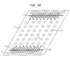
- FIG. 5is a top perspective view of a frame used in the method of the present invention.
- FIG. 6is a top perspective view of the frame of FIG. 5 after a sheet of dielectric “tape” has been applied to the bottom surface.
- FIG. 6 ais an exploded view of a portion of FIG. 6 depicting circuit features on the tape.
- FIG. 7 ais a top perspective view of the frame of FIG. 6 after a plurality of microelectronic elements have been attached to the tape.
- FIG. 7 bis a bottom perspective view of the frame of FIG. 6 after the plurality of microelectronic elements have been attached to the tape.
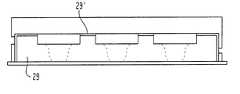
- FIG. 8is a top perspective view of the frame of FIG. 7 a after a coverlay has been attached to the top surface of the frame.
- FIG. 9is a top perspective view of the frame of FIG. 8 after a thixotropic encapsulant composition has been applied between the tape and the coverlay, and cured.
- FIG. 10is perspective view of a plurality of semiconductor chip devices packaged according to a method of the prior art wherein the need to contain the encapsulant until the cure process is completed in order to prevent flow out of the encapsulant.
- FIGS. 11-14depict various microelectronic elements that can be made using the methods of the present invention.
- FIG. 11is a side view of a fan-in type semiconductor chip package.
- FIG. 12is a side view of a fan-out type semiconductor chip package.
- FIG. 13is a side view of a fan-in/fan-out type semiconductor chip package.
- FIG. 14is a side view of a wafer scale package.
- FIGS. 15-17depict progressive steps in another embodiment of the present invention.
- FIG. 15is a side view of the work-piece of FIG. 1 after it has been placed in a mold and a liquid composition has begun to be dispensed into the mold cavity.
- FIG. 16is a side view of the work-piece of FIG. 15 after the mold cavity has been filled with a liquid encapsulant composition and after a portion of such composition has been cured to form a cured skin.
- FIG. 17is a side view of the work-piece of FIG. 16 after the work-piece has been removed from the mold and the remaining uncured portions of the liquid composition have subsequently been cured to form a complaint encapsulant.
- the present inventionrelates to a method of making a semiconductor chip package using a thixotropic encapsulating composition. Progressive steps in the method of this aspect of the invention are depicted in FIGS. 1-4. Such figures, as well as the FIGS. 5-17, are not drawn to scale. Some of the dimensions in such figures are exaggerated to better describe the methods of the present invention.
- the method of this aspect of the present inventionincludes the step of attaching at least one microelectronic element 20 to a dielectric layer 21 via element 22 .
- the microelectronic elementmay be a semiconductor chip, a plurality of such chips or a plurality of such chips disposed on a wafer. There are three semiconductor chips 20 attached to dielectric layer 21 in FIG.
- a mold 23which is capable of being sealingly engaged with the dielectric layer, is provided.
- the dielectric layer and the attached semiconductor chipsare placed in mold 23 .
- Mold 23is equipped with one or more inlet ports 24 .
- Mold 23may also be equipped with a vacuum port for connecting a vacuum pump so that a vacuum environment may be created within mold 23 .
- a needle 26is inserted in inlet port 24 .
- a thixotropic composition 28is dispensed or injected through the needle 26 into the cavity created by mold 23 . As thixotropic composition 28 flows through needle 26 , it is exposed to a shearing force which reduces its viscosity.
- thixotropic composition 28is injected into the cavity created by mold 23 until the area between the chips 20 and the dielectric layer 21 is completely filled.
- compositions that are suitable for use a thixotropic compositionmust be capable of curing to form cured encapsulants. In preferred embodiments, such compositions cure upon exposure to heat. Such compositions should also be sufficiently pseudoplastic to allow the composition to completely flow between the areas between the microelectronic elements and the dielectric layer after being dispensed from the dispense needle.
- a pseudoplastic fluidis defined as a material whose viscosity decreases upon exposure to a shear force. The decrease in viscosity with increasing shear rate, which is a defining characteristic of pseudoplastic fluids, is believed to be the result of a number of factors. One of those factors is the degree of aggregation of filler materials in the fluid.
- filler particle aggregatesmay be broken down thereby reducing the viscosity of the fluid.
- Another characteristic of a fluid that may result in pseudoplastic propertiesis the ability of the molecules of the fluid to be aligned. Long polymeric molecules may de-tangle and align in the direction of shear during a shearing process.
- the compositionmust also be sufficiently thixotropic to prevent flow-out of the composition when the mold is removed.
- a thixotropic fluidis defined as a pseudoplastic fluid that will regain some or all of its initial viscosity when the shear force is removed. Some thixotropic materials require an extended rest period to regain viscosity after the cessation of the application of the shear force.
- Such rest periodis also sometimes referred to as a “re-gel” time.
- Other thixotropic materialsregain viscosity quite rapidly.
- the time required, after the shear force is removed, for composition 28 to regain sufficient viscosity to prevent flow-outis less than 1 minute, more preferably less than 10 seconds.
- the initial viscosity of the thixotropic compositionis greater than 100,000 centipoise at 25 C., more preferably greater than 150,000 centipoise at 25 C.; and the reduced viscosity is less than 10,000 centipoise at 25 C.; and the time period required for the thixotropic composition to regain 65% of its initial viscosity is less than 1 minute, more preferably less than 10 seconds.
- the thixotropic compositioncures to form an encapsulant that is preferably selected from the group consisting of silicone elastomers, silicone gels, epoxies, and flexiblized epoxies.
- the viscosity of some pseudoplastic and some thixotropic materialsis only effected within a certain range of shear rates.
- Thixotropic composition 28 and the dispense conditionsshould be selected such that the viscosity of composition 28 will be sufficiently low upon exiting the dispense needle 26 to completely fill the areas between the microelectronic elements and dielectric layer 21 and such that the viscosity of composition 28 will be sufficiently high upon the removal of mold 23 to prevent flow-out.
- the shear forcemay continued to be applied in order to maintain the low viscosity of the composition and to insure that each microelectronic element is encapsulated as desired.
- the shear forcemay be reduced or removed. Once the shear force is removed the thixotropic material will begin to regain some or all of its initial higher viscosity.
- thixotropic composition 28should remain in mold 23 until its viscosity has increased sufficiently to prevent composition 28 from flowing prior to and during the curing step. Mold 23 may then be removed, as depicted in FIG. 4 . Dielectric layer 21 , microelectronic element(s) 20 and composition 28 are then placed in a curing oven for a time and at a temperature sufficient to cure composition 28 to form a cured encapsulant 28 ′.
- composition 28is only partially cured, to the extent necessary to prevent the composition from flowing out of the assembly, before the assembly is removed from the curing oven.
- the partially cured skinmay be formed by exposing the composition 28 to ultraviolet radiation, to an electronic beam, to X-rays, to moisture, to air and/or heat.
- Composition 28may then be fully cured to form cured encapsulant 28 ′ in a later processing step.
- a plurality of conductive connection elementssuch as solder balls, may be disposed on the bottom surface of the dielectric layer.
- Each of solderballcan be electrically connected to one of the leads to provide a means for connecting a packaged semiconductor chip to a substrate.
- the dielectric layermay then be diced to form a plurality of individual semiconductor devices.
- the dielectric sheetis flexible.
- the dielectric sheetis comprised of a polyimide.
- the present inventionalso relates to a method of making a semiconductor chip package without using a mold. Progressive steps in one embodiment of this aspect of the present invention are depicted in FIGS. 5-14.
- a frame 1is provided.
- the frameaids in handling aligning the dielectric layer during the various processing steps.
- Frame 1unlike the mold or fixture referenced above, does not need to be sealingly engaged with the dielectric layer.
- Frame 1has a central opening, which in preferred embodiments is sized to accommodate a 35 mm or 70 mm wide stripe of a dielectric sheet.
- the central openingalso preferably includes two radially like extension disposed on opposite ends of the frame. One of the radially like extensions, 2 , may be used as a dispense port.
- the other radially like extension, 3may be used as another dispense port, or more preferably, as a vacuum port.
- Frame 1also has a top surface 11 and a bottom surface 10 .
- a dielectric sheet 4is attached to the bottom surface 10 of frame 1 .
- Dielectric sheet 4has a least one region 5 having a plurality of circuit features.
- the dielectric sheet depicted in FIG. 6has three such regions 5 .
- FIG. 6 ais an exploded view of one of the regions 5 .
- the plurality of circuit featuresinclude a plurality of compliant spacer 6 , and a plurality of electrically conductive leads 8 .
- Each lead 8has a tip end which is connected to a bus bar 9 and a terminal end which is connected to an electrically conductive terminal 16 . A portion of each lead 8 is disposed over a bond window 7 .
- a face surface of a microelectronic element 12is attached to each region 5 of dielectric layer 4 .
- each microelectronic element 12may be a semiconductor chip.
- Microelectronic element 12may also be a plurality of semiconductor chips or an interconnected plurality of such chips disposed on a wafer.
- the step of attaching each microelectronic element 12 to each region 5may include the use of a die attach adhesive.
- FIG. 7 bis a bottom perspective view of the assembly of FIG. 7 a.
- FIG. 8is a top perspective view of the assembly of FIG. 7 a after a coverlay 13 is disposed over dielectric sheet 4 and attached to the top surface 11 of frame 1 .
- the coverlay materialis made of a thin sheet of polyimide.
- a thixotropic compositionis disposed between the coverlay and the dielectric sheet.
- the disposing stepincludes a step selected from dispensing and injection the thixotropic composition. Prior to or during the disposing step, the thixotropic composition, is subjected to a shearing force to reduce its viscosity.
- Shearing forces which may be usedinclude such processes as stirring, mixing, rolling and/or forcing the composition through an orifice.
- Features on the dielectric sheet, such as the compliant spacersmay be used as viscosity reducing agents by subjecting the thixotropic composition to a shearing forces as such composition flows past and between such features.
- the thixotropic compositionshould be curable to form a cured encapsulant.
- the time required, after the shear force is removed, for composition 28 to regain sufficient viscosity to prevent flow-outis less than 1 minute, more preferably less than 10 seconds.
- the initial viscosity of the thixotropic compositionis greater than 100,000 centipoise at 25 C., more preferably greater than 150,000 centipoise at 25 C.; and the reduced viscosity is less than 10,000 centipoise at 25 C.; and the time period required for the thixotropic composition to regain 65% of its initial viscosity is less than 1 minute. more preferably less than 10 seconds.
- the thixotropic compositioncures to form an encapsulant that is preferably selected from the group consisting of silicone elastomers, silicone gels and flexibilized epoxies.
- the dielectric sheetis flexible.
- the dielectric sheetis comprised of a polyimide.
- the time and/or the energy required to make a semiconductor chip packagemay be reduced because the time and/or the energy needed to cure the encapsulant composition is reduced.
- Production efficienciesmay also be achieved by curing the encapsulant “off-line” (i.e. out of the mold or dispense machine) so that another package or set of packages may be encapsulated in such mold or machine, thereby increasing the production throughput.
- coverlay 13is replaced by a platen which is juxtaposed with the top surface 11 of frame 1 before the thixotropic composition is dispensed or injected onto dielectric layer 4 .
- the platenIn order to maintain the planarity of the resulting package, the platen must be substantially rigid and must remain fixed against the top surface of the frame during the encapsulation dispense operation.
- the platenmay be equipped with a release liner or release surface, such as polytrifluoroethylene (“PTFE”), to prevent the cured encapsulant from adhering to the platen when the thixotropic composition cures.
- PTFEpolytrifluoroethylene
- the reduced viscosity of the sheared thixotropic compoundwill be low enough to allow the composition to flow between the semiconductor chip 12 and the associated region 5 of the dielectric layer 4 and to fill the areas between such chips 12 and regions 5 .
- the shearing forcemay be applied before the thixotropic composition is dispensed onto the dielectric layer, by for example, stirring the composition.
- the shearing forcemay be applied as the thixotropic composition is being dispensed onto the dielectric layer by dispensing the composition through a needle.
- the shearing force on the thixotropic compositionis maintain until after the thixotropic composition has been dispensed by using a pressure injection system to dispense the composition.
- the thixotropic compositionshould remain under shear and with the accompanying reduced viscosity, until the areas between the chips 12 and the regions 5 are filled as desired.
- the thixotropic compositionis curable to form a silicone elastomer, a silicone gel, an epoxy, or a flexiblized epoxy.
- the assembly of FIG. 9may be removed from the frame and cured in a curing oven.
- the frame with the assembly attachedmay be cured in a curing oven.
- the frameis constructed of a thin sheet of a reinforced epoxy such as Norplex CEM-1.
- the shear forcemay be continued to be applied in order to maintain the low viscosity of the composition and to insure that each microelectronic element is encapsulated as desired.
- the area between the dielectric layer and the microelectronic elements or the cover layermay be completely filled to completely encapsulate each microelectronic element or partially filled to partially encapsulate one or more of such microelectronic elements.
- the assemblymay be diced to form a plurality of semiconductor chip packages.
- a cross-sectional side view of the diced semiconductor chip packageis depicted in FIG. 11 .
- the semiconductor chip package depicted in FIG. 11is a so-called “fan-in” type package.
- the method of the present inventionmay be used to make fan-in, fan-out, fan-in/fan-out and array area type packages.
- the chip contactsare located within the periphery of the chip, each corresponding terminal is located on the flexible dielectric layer in a region that is closer to the center of the chip and each lead fans inwardly from a chip contact to a terminal.
- each corresponding terminalis located on the flexible dielectric layer in a region that is farther from the center of the chip and each lead fans outwardly from a chip contact to the corresponding terminal.
- a packagemay be made, for example, as disclosed in commonly assigned U.S. Pat. Nos. 5,688,716; 5,148,265; and U.S. patent application Ser. No. 08/365,749 filed on Dec. 28, 1994, the disclosures of which are incorporated by reference herein.
- FIG. 13in a fan-in/fan-out arrangement, some of the leads fan-in and some fan-out.
- Such a packagemay be made, for example, as disclosed in the aforementioned '265 patent and '749 patent application.
- the terminalsare typically disposed in single rows and columns on the flexible dielectric layer, but may be disposed in a so called “area array”, a grid like array on the primary surface of the flexible dielectric layer.
- a wafer scale package with an terminals arranged in an area arrayis depicted in FIG. 14 .
- Such a packagemay be made, for example, as disclosed in commonly assigned U.S. Pat. Nos. 5,518,964; and 5,455,390, the disclosures of which are hereby incorporated by reference herein.
- a conductive adhesive, solder balls, solder or any other suitable bonding methodmay be used to bond each terminal to the corresponding connection pad on a support substrate.
- FIG. 10is a top perspective view of a frame and a plurality of semiconductor chip packages of the prior art.
- the packageswere manufactured according to the method of the present invention except that the encapsulant used did not have any or sufficient thixotropic properties to prevent the encapsulant composition from leaking or backflowing from the assembly.
- the present inventionalso relates to a method of packaging a semiconductor chip without using a mold during the encapsulant curing step and without the need to use a thixotropic encapsulating composition.
- the method of this aspect of the inventionincludes the step depicted in FIG. 1, wherein a dielectric layer 21 having at least one microelectronic element 20 is provided. Subsequent steps in the method of this aspect of the invention are depicted in FIGS. 15-17.
- mold 23is sealingly engaged with dielectric layer 21 .
- Mold 23has at least one inlet port 24 and may have one or more vacuum ports 25 .
- a dispense needle 26is used to dispense a liquid composition 29 through inlet port 24 and into the mold cavity to fill the area between the microelectronic elements and the dielectric layer.
- a portion of liquid composition 29is cured to form a cured skin of encapsulant 29 ′.
- mold 23may then be removed and the uncured portion of liquid composition 29 is cured to form a cured encapsulant 29 ′.
- the liquid compositionis curable to form an encapsulant selected from the group consisting of silicone elastomers, silicone gels and flexiblized epoxies.
- the dielectric sheetis preferably flexible. In particularly preferred embodiments, the dielectric sheet is comprised of a polyimide.
- the methods of the present inventioncan be used at the wafer level to encapsulate an entire wafer by replacing the semiconductor chip with a wafer.
Landscapes
- Engineering & Computer Science (AREA)
- Physics & Mathematics (AREA)
- Condensed Matter Physics & Semiconductors (AREA)
- General Physics & Mathematics (AREA)
- Manufacturing & Machinery (AREA)
- Computer Hardware Design (AREA)
- Microelectronics & Electronic Packaging (AREA)
- Power Engineering (AREA)
- Encapsulation Of And Coatings For Semiconductor Or Solid State Devices (AREA)
- Structures Or Materials For Encapsulating Or Coating Semiconductor Devices Or Solid State Devices (AREA)
Abstract
Description
Claims (8)
Priority Applications (1)
| Application Number | Priority Date | Filing Date | Title |
|---|---|---|---|
| US09/712,635US6458628B1 (en) | 1997-10-15 | 2000-11-14 | Methods of encapsulating a semiconductor chip using a settable encapsulant |
Applications Claiming Priority (4)
| Application Number | Priority Date | Filing Date | Title |
|---|---|---|---|
| US6247197P | 1997-10-15 | 1997-10-15 | |
| US09/166,812US6080605A (en) | 1998-10-06 | 1998-10-06 | Methods of encapsulating a semiconductor chip using a settable encapsulant |
| US09/520,357US6218215B1 (en) | 1997-10-15 | 2000-03-07 | Methods of encapsulating a semiconductor chip using a settable encapsulant |
| US09/712,635US6458628B1 (en) | 1997-10-15 | 2000-11-14 | Methods of encapsulating a semiconductor chip using a settable encapsulant |
Related Parent Applications (1)
| Application Number | Title | Priority Date | Filing Date |
|---|---|---|---|
| US09/520,357DivisionUS6218215B1 (en) | 1997-10-15 | 2000-03-07 | Methods of encapsulating a semiconductor chip using a settable encapsulant |
Publications (1)
| Publication Number | Publication Date |
|---|---|
| US6458628B1true US6458628B1 (en) | 2002-10-01 |
Family
ID=22604789
Family Applications (3)
| Application Number | Title | Priority Date | Filing Date |
|---|---|---|---|
| US09/166,812Expired - LifetimeUS6080605A (en) | 1997-10-15 | 1998-10-06 | Methods of encapsulating a semiconductor chip using a settable encapsulant |
| US09/520,357Expired - LifetimeUS6218215B1 (en) | 1997-10-15 | 2000-03-07 | Methods of encapsulating a semiconductor chip using a settable encapsulant |
| US09/712,635Expired - LifetimeUS6458628B1 (en) | 1997-10-15 | 2000-11-14 | Methods of encapsulating a semiconductor chip using a settable encapsulant |
Family Applications Before (2)
| Application Number | Title | Priority Date | Filing Date |
|---|---|---|---|
| US09/166,812Expired - LifetimeUS6080605A (en) | 1997-10-15 | 1998-10-06 | Methods of encapsulating a semiconductor chip using a settable encapsulant |
| US09/520,357Expired - LifetimeUS6218215B1 (en) | 1997-10-15 | 2000-03-07 | Methods of encapsulating a semiconductor chip using a settable encapsulant |
Country Status (1)
| Country | Link |
|---|---|
| US (3) | US6080605A (en) |
Cited By (25)
| Publication number | Priority date | Publication date | Assignee | Title |
|---|---|---|---|---|
| US20030173051A1 (en)* | 2002-03-12 | 2003-09-18 | Intel Corporation | Semi-solid metal injection methods and apparatus for electronic assembly thermal interface |
| US20050130336A1 (en)* | 2003-12-15 | 2005-06-16 | Collins William D.Iii | Method of packaging a semiconductor light emitting device |
| WO2005071732A1 (en)* | 2004-01-22 | 2005-08-04 | Fico B.V. | Carrier for electronic components and methods for encapsulating and separating an electronic component |
| WO2005091361A1 (en)* | 2004-03-19 | 2005-09-29 | Dow Corning Toray Co., Ltd. | Semiconductor device and method of manufacturing thereof |
| US20060003137A1 (en)* | 2004-07-02 | 2006-01-05 | Amstutz Aaron K | System and method for encapsulation and protection of components |
| US20070230131A1 (en)* | 2003-01-16 | 2007-10-04 | Bunyan Michael H | Dispensable cured resin |
| US20110018137A1 (en)* | 2009-07-23 | 2011-01-27 | Nec Electronics Corporation | Method of manufacturing semiconductor device, semiconductor device thus manufactured, and semiconductor manufacturing apparatus |
| US7960272B2 (en) | 2002-10-24 | 2011-06-14 | Megica Corporation | Method for fabricating thermal compliant semiconductor chip wiring structure for chip scale packaging |
| US20110183496A1 (en)* | 2010-01-26 | 2011-07-28 | Oki Semiconductor Co., Ltd. | Method of manufacturing a semiconductor device and substrate carrier structure |
| US8426982B2 (en) | 2001-03-30 | 2013-04-23 | Megica Corporation | Structure and manufacturing method of chip scale package |
| US20150176851A1 (en)* | 2013-12-19 | 2015-06-25 | Airius Ip Holdings, Llc | Columnar air moving devices, systems and methods |
| US20160120039A1 (en)* | 2014-10-23 | 2016-04-28 | Samsung Electronics Co., Ltd. | Method of manufacturing printed-circuit board assembly |
| US9459020B2 (en) | 2008-05-30 | 2016-10-04 | Airius Ip Holdings, Llc | Columnar air moving devices, systems and methods |
| USD783795S1 (en) | 2012-05-15 | 2017-04-11 | Airius Ip Holdings, Llc | Air moving device |
| US9631627B2 (en) | 2004-03-15 | 2017-04-25 | Airius Ip Holdings, Llc | Columnar air moving devices, systems and methods |
| USD805176S1 (en) | 2016-05-06 | 2017-12-12 | Airius Ip Holdings, Llc | Air moving device |
| US9970457B2 (en) | 2008-05-30 | 2018-05-15 | Airius Ip Holdings, Llc | Columnar air moving devices, systems and methods |
| USD820967S1 (en) | 2016-05-06 | 2018-06-19 | Airius Ip Holdings Llc | Air moving device |
| US10024531B2 (en) | 2013-12-19 | 2018-07-17 | Airius Ip Holdings, Llc | Columnar air moving devices, systems and methods |
| US10221861B2 (en) | 2014-06-06 | 2019-03-05 | Airius Ip Holdings Llc | Columnar air moving devices, systems and methods |
| US10487852B2 (en) | 2016-06-24 | 2019-11-26 | Airius Ip Holdings, Llc | Air moving device |
| USD885550S1 (en) | 2017-07-31 | 2020-05-26 | Airius Ip Holdings, Llc | Air moving device |
| USD886275S1 (en) | 2017-01-26 | 2020-06-02 | Airius Ip Holdings, Llc | Air moving device |
| USD887541S1 (en) | 2019-03-21 | 2020-06-16 | Airius Ip Holdings, Llc | Air moving device |
| US11598539B2 (en) | 2019-04-17 | 2023-03-07 | Airius Ip Holdings, Llc | Air moving device with bypass intake |
Families Citing this family (32)
| Publication number | Priority date | Publication date | Assignee | Title |
|---|---|---|---|---|
| US6713151B1 (en)* | 1998-06-24 | 2004-03-30 | Honeywell International Inc. | Compliant fibrous thermal interface |
| US6436506B1 (en)* | 1998-06-24 | 2002-08-20 | Honeywell International Inc. | Transferrable compliant fibrous thermal interface |
| WO1999067811A2 (en) | 1998-06-24 | 1999-12-29 | Johnson Matthey Electronics, Inc. | Electronic device having fibrous interface |
| US6103552A (en)* | 1998-08-10 | 2000-08-15 | Lin; Mou-Shiung | Wafer scale packaging scheme |
| US6812718B1 (en) | 1999-05-27 | 2004-11-02 | Nanonexus, Inc. | Massively parallel interface for electronic circuits |
| US7349223B2 (en) | 2000-05-23 | 2008-03-25 | Nanonexus, Inc. | Enhanced compliant probe card systems having improved planarity |
| US7247035B2 (en)* | 2000-06-20 | 2007-07-24 | Nanonexus, Inc. | Enhanced stress metal spring contactor |
| US7382142B2 (en) | 2000-05-23 | 2008-06-03 | Nanonexus, Inc. | High density interconnect system having rapid fabrication cycle |
| US6559388B1 (en)* | 1999-06-08 | 2003-05-06 | International Business Machines Corporation | Strain relief for substrates having a low coefficient of thermal expansion |
| US6255142B1 (en)* | 1999-10-29 | 2001-07-03 | Nordson Corporation | Method for underfilling semiconductor devices |
| US6602740B1 (en) | 1999-11-24 | 2003-08-05 | Tessera, Inc. | Encapsulation of microelectronic assemblies |
| US6644238B2 (en) | 2000-01-28 | 2003-11-11 | Speedline Technologies, Inc. | Conveyorized vacuum injection system |
| US6664621B2 (en)* | 2000-05-08 | 2003-12-16 | Tessera, Inc. | Semiconductor chip package with interconnect structure |
| US7952373B2 (en) | 2000-05-23 | 2011-05-31 | Verigy (Singapore) Pte. Ltd. | Construction structures and manufacturing processes for integrated circuit wafer probe card assemblies |
| US7579848B2 (en) | 2000-05-23 | 2009-08-25 | Nanonexus, Inc. | High density interconnect system for IC packages and interconnect assemblies |
| ATE311604T1 (en) | 2000-06-20 | 2005-12-15 | Nanonexus Inc | INTEGRATED CIRCUIT TEST SYSTEM |
| JP2002198471A (en)* | 2000-12-22 | 2002-07-12 | Aisin Aw Co Ltd | Electronic control unit |
| JP2005514760A (en)* | 2001-07-09 | 2005-05-19 | ノードソン コーポレーション | Method and apparatus for underfilling electronic components using vacuum assist |
| DE10145468C1 (en) | 2001-09-14 | 2003-01-16 | Infineon Technologies Ag | Process for fixing a semiconductor device on a switching device, used in flip-chip technology, comprises preparing a semiconductor device with bond pads on one surface |
| TW504824B (en)* | 2001-11-21 | 2002-10-01 | Siliconware Precision Industries Co Ltd | Semiconductor package having chip cracking prevention member |
| TW544882B (en)* | 2001-12-31 | 2003-08-01 | Megic Corp | Chip package structure and process thereof |
| US6673698B1 (en)* | 2002-01-19 | 2004-01-06 | Megic Corporation | Thin film semiconductor package utilizing a glass substrate with composite polymer/metal interconnect layers |
| TW584950B (en) | 2001-12-31 | 2004-04-21 | Megic Corp | Chip packaging structure and process thereof |
| TW517361B (en) | 2001-12-31 | 2003-01-11 | Megic Corp | Chip package structure and its manufacture process |
| TW503496B (en)* | 2001-12-31 | 2002-09-21 | Megic Corp | Chip packaging structure and manufacturing process of the same |
| US6861278B2 (en)* | 2002-04-11 | 2005-03-01 | Nordson Corporation | Method and apparatus for underfilling semiconductor devices |
| US7344505B2 (en)* | 2002-10-15 | 2008-03-18 | Transoma Medical, Inc. | Barriers and methods for pressure measurement catheters |
| DE10343498A1 (en)* | 2003-02-07 | 2005-05-04 | Univ Leipzig | Method for determining at least one state parameter of a sealing system and sealing system |
| US6858466B1 (en)* | 2003-11-03 | 2005-02-22 | Hewlett-Packard Development Company, L.P. | System and a method for fluid filling wafer level packages |
| US7569422B2 (en)* | 2006-08-11 | 2009-08-04 | Megica Corporation | Chip package and method for fabricating the same |
| US8877567B2 (en)* | 2010-11-18 | 2014-11-04 | Stats Chippac, Ltd. | Semiconductor device and method of forming uniform height insulating layer over interposer frame as standoff for semiconductor die |
| US9543277B1 (en)* | 2015-08-20 | 2017-01-10 | Invensas Corporation | Wafer level packages with mechanically decoupled fan-in and fan-out areas |
Citations (16)
| Publication number | Priority date | Publication date | Assignee | Title |
|---|---|---|---|---|
| US4340551A (en)* | 1980-08-11 | 1982-07-20 | Asahi-Dow Limited | Injection molded articles with improved surface characteristics, production of same and apparatus therefor |
| US4592928A (en) | 1985-01-09 | 1986-06-03 | Dow Corning Corporation | Method and compositions for inhibiting leakage current in silicon diodes |
| US4868349A (en)* | 1988-05-09 | 1989-09-19 | National Semiconductor Corporation | Plastic molded pin-grid-array power package |
| US4996170A (en) | 1990-07-30 | 1991-02-26 | Motorola, Inc. | Molding process for encapsulating semiconductor devices using a thixotropic compound |
| US5148265A (en) | 1990-09-24 | 1992-09-15 | Ist Associates, Inc. | Semiconductor chip assemblies with fan-in leads |
| US5225023A (en) | 1989-02-21 | 1993-07-06 | General Electric Company | High density interconnect thermoplastic die attach material and solvent die attach processing |
| US5272113A (en) | 1992-11-12 | 1993-12-21 | Xerox Corporation | Method for minimizing stress between semiconductor chips having a coefficient of thermal expansion different from that of a mounting substrate |
| US5455390A (en) | 1994-02-01 | 1995-10-03 | Tessera, Inc. | Microelectronics unit mounting with multiple lead bonding |
| US5518964A (en) | 1994-07-07 | 1996-05-21 | Tessera, Inc. | Microelectronic mounting with multiple lead deformation and bonding |
| US5659652A (en) | 1995-09-29 | 1997-08-19 | D'entremont; Joseph P. | Support system for rapid assembly of component infrastructures |
| US5659952A (en)* | 1994-09-20 | 1997-08-26 | Tessera, Inc. | Method of fabricating compliant interface for semiconductor chip |
| US5688716A (en) | 1994-07-07 | 1997-11-18 | Tessera, Inc. | Fan-out semiconductor chip assembly |
| US5766987A (en) | 1995-09-22 | 1998-06-16 | Tessera, Inc. | Microelectronic encapsulation methods and equipment |
| US5773322A (en) | 1995-05-01 | 1998-06-30 | Lucent Technologies Inc. | Molded encapsulated electronic component |
| US5776796A (en) | 1994-05-19 | 1998-07-07 | Tessera, Inc. | Method of encapsulating a semiconductor package |
| US5955021A (en)* | 1997-05-19 | 1999-09-21 | Cardxx, Llc | Method of making smart cards |
- 1998
- 1998-10-06USUS09/166,812patent/US6080605A/ennot_activeExpired - Lifetime
- 2000
- 2000-03-07USUS09/520,357patent/US6218215B1/ennot_activeExpired - Lifetime
- 2000-11-14USUS09/712,635patent/US6458628B1/ennot_activeExpired - Lifetime
Patent Citations (17)
| Publication number | Priority date | Publication date | Assignee | Title |
|---|---|---|---|---|
| US4340551A (en)* | 1980-08-11 | 1982-07-20 | Asahi-Dow Limited | Injection molded articles with improved surface characteristics, production of same and apparatus therefor |
| US4592928A (en) | 1985-01-09 | 1986-06-03 | Dow Corning Corporation | Method and compositions for inhibiting leakage current in silicon diodes |
| US4868349A (en)* | 1988-05-09 | 1989-09-19 | National Semiconductor Corporation | Plastic molded pin-grid-array power package |
| US5225023A (en) | 1989-02-21 | 1993-07-06 | General Electric Company | High density interconnect thermoplastic die attach material and solvent die attach processing |
| US5348607A (en) | 1989-02-21 | 1994-09-20 | General Electric Company | High density interconnect thermoplastic die attach material and solvent die attach processing |
| US4996170A (en) | 1990-07-30 | 1991-02-26 | Motorola, Inc. | Molding process for encapsulating semiconductor devices using a thixotropic compound |
| US5148265A (en) | 1990-09-24 | 1992-09-15 | Ist Associates, Inc. | Semiconductor chip assemblies with fan-in leads |
| US5272113A (en) | 1992-11-12 | 1993-12-21 | Xerox Corporation | Method for minimizing stress between semiconductor chips having a coefficient of thermal expansion different from that of a mounting substrate |
| US5455390A (en) | 1994-02-01 | 1995-10-03 | Tessera, Inc. | Microelectronics unit mounting with multiple lead bonding |
| US5776796A (en) | 1994-05-19 | 1998-07-07 | Tessera, Inc. | Method of encapsulating a semiconductor package |
| US5518964A (en) | 1994-07-07 | 1996-05-21 | Tessera, Inc. | Microelectronic mounting with multiple lead deformation and bonding |
| US5688716A (en) | 1994-07-07 | 1997-11-18 | Tessera, Inc. | Fan-out semiconductor chip assembly |
| US5659952A (en)* | 1994-09-20 | 1997-08-26 | Tessera, Inc. | Method of fabricating compliant interface for semiconductor chip |
| US5773322A (en) | 1995-05-01 | 1998-06-30 | Lucent Technologies Inc. | Molded encapsulated electronic component |
| US5766987A (en) | 1995-09-22 | 1998-06-16 | Tessera, Inc. | Microelectronic encapsulation methods and equipment |
| US5659652A (en) | 1995-09-29 | 1997-08-19 | D'entremont; Joseph P. | Support system for rapid assembly of component infrastructures |
| US5955021A (en)* | 1997-05-19 | 1999-09-21 | Cardxx, Llc | Method of making smart cards |
Non-Patent Citations (1)
| Title |
|---|
| HAAKE, rheometers, pp. 12-21. |
Cited By (59)
| Publication number | Priority date | Publication date | Assignee | Title |
|---|---|---|---|---|
| US8426982B2 (en) | 2001-03-30 | 2013-04-23 | Megica Corporation | Structure and manufacturing method of chip scale package |
| US9018774B2 (en) | 2001-03-30 | 2015-04-28 | Qualcomm Incorporated | Chip package |
| US8912666B2 (en) | 2001-03-30 | 2014-12-16 | Qualcomm Incorporated | Structure and manufacturing method of chip scale package |
| US8748227B2 (en) | 2001-03-30 | 2014-06-10 | Megit Acquisition Corp. | Method of fabricating chip package |
| US6787899B2 (en)* | 2002-03-12 | 2004-09-07 | Intel Corporation | Electronic assemblies with solidified thixotropic thermal interface material |
| US20030173051A1 (en)* | 2002-03-12 | 2003-09-18 | Intel Corporation | Semi-solid metal injection methods and apparatus for electronic assembly thermal interface |
| US7169650B2 (en) | 2002-03-12 | 2007-01-30 | Intel Corporation | Semi-solid metal injection methods for electronic assembly thermal interface |
| US7960272B2 (en) | 2002-10-24 | 2011-06-14 | Megica Corporation | Method for fabricating thermal compliant semiconductor chip wiring structure for chip scale packaging |
| US8334588B2 (en) | 2002-10-24 | 2012-12-18 | Megica Corporation | Circuit component with conductive layer structure |
| US8119191B2 (en)* | 2003-01-16 | 2012-02-21 | Parker-Hannifin Corporation | Dispensable cured resin |
| US20070230131A1 (en)* | 2003-01-16 | 2007-10-04 | Bunyan Michael H | Dispensable cured resin |
| US7087465B2 (en)* | 2003-12-15 | 2006-08-08 | Philips Lumileds Lighting Company, Llc | Method of packaging a semiconductor light emitting device |
| US20050130336A1 (en)* | 2003-12-15 | 2005-06-16 | Collins William D.Iii | Method of packaging a semiconductor light emitting device |
| TWI467705B (en)* | 2004-01-22 | 2015-01-01 | Besi Netherlands Bv | Carrier for electronic components and methods for encapsulating and separating an electronic component |
| WO2005071732A1 (en)* | 2004-01-22 | 2005-08-04 | Fico B.V. | Carrier for electronic components and methods for encapsulating and separating an electronic component |
| US11703062B2 (en) | 2004-03-15 | 2023-07-18 | Airius Ip Holdings, Llc | Temperature destratification systems |
| US9714663B1 (en) | 2004-03-15 | 2017-07-25 | Airius Ip Holdings, Llc | Temperature destratification systems |
| US10487840B2 (en) | 2004-03-15 | 2019-11-26 | Airius Ip Holdings, Llc | Temperature destratification systems |
| US9631627B2 (en) | 2004-03-15 | 2017-04-25 | Airius Ip Holdings, Llc | Columnar air moving devices, systems and methods |
| US11053948B2 (en) | 2004-03-15 | 2021-07-06 | Airius Ip Holdings, Llc | Temperature destratification systems |
| US11365743B2 (en) | 2004-03-15 | 2022-06-21 | Airius Ip Holdings, Llc | Temperature destratification systems |
| US12085084B2 (en) | 2004-03-15 | 2024-09-10 | Airius Ip Holdings, Llc | Temperature destratification systems |
| US8262970B2 (en) | 2004-03-19 | 2012-09-11 | Dow Corning Toray Company, Ltd. | Semiconductor device and method of manufacturing thereof |
| WO2005091361A1 (en)* | 2004-03-19 | 2005-09-29 | Dow Corning Toray Co., Ltd. | Semiconductor device and method of manufacturing thereof |
| US7390551B2 (en) | 2004-07-02 | 2008-06-24 | Caterpillar Inc. | System and method for encapsulation and protection of components |
| US20060003137A1 (en)* | 2004-07-02 | 2006-01-05 | Amstutz Aaron K | System and method for encapsulation and protection of components |
| US9459020B2 (en) | 2008-05-30 | 2016-10-04 | Airius Ip Holdings, Llc | Columnar air moving devices, systems and methods |
| US9970457B2 (en) | 2008-05-30 | 2018-05-15 | Airius Ip Holdings, Llc | Columnar air moving devices, systems and methods |
| US20110018137A1 (en)* | 2009-07-23 | 2011-01-27 | Nec Electronics Corporation | Method of manufacturing semiconductor device, semiconductor device thus manufactured, and semiconductor manufacturing apparatus |
| US8541300B2 (en)* | 2009-07-23 | 2013-09-24 | Renesas Electronics Corporation | Method of manufacturing semiconductor device, semiconductor device thus manufactured, and semiconductor manufacturing apparatus |
| US8216919B2 (en)* | 2010-01-26 | 2012-07-10 | Oki Semiconductor Co., Ltd. | Method of manufacturing a semiconductor device and substrate carrier structure |
| US20110183496A1 (en)* | 2010-01-26 | 2011-07-28 | Oki Semiconductor Co., Ltd. | Method of manufacturing a semiconductor device and substrate carrier structure |
| US10184489B2 (en) | 2011-06-15 | 2019-01-22 | Airius Ip Holdings, Llc | Columnar air moving devices, systems and methods |
| USD783795S1 (en) | 2012-05-15 | 2017-04-11 | Airius Ip Holdings, Llc | Air moving device |
| USD926963S1 (en) | 2012-05-15 | 2021-08-03 | Airius Ip Holdings, Llc | Air moving device |
| US20150176851A1 (en)* | 2013-12-19 | 2015-06-25 | Airius Ip Holdings, Llc | Columnar air moving devices, systems and methods |
| US10024531B2 (en) | 2013-12-19 | 2018-07-17 | Airius Ip Holdings, Llc | Columnar air moving devices, systems and methods |
| US11221153B2 (en) | 2013-12-19 | 2022-01-11 | Airius Ip Holdings, Llc | Columnar air moving devices, systems and methods |
| US11092330B2 (en) | 2013-12-19 | 2021-08-17 | Airius Ip Holdings, Llc | Columnar air moving devices, systems and methods |
| US10641506B2 (en) | 2013-12-19 | 2020-05-05 | Airius Ip Holdings, Llc | Columnar air moving devices, systems and methods |
| US10655841B2 (en) | 2013-12-19 | 2020-05-19 | Airius Ip Holdings, Llc | Columnar air moving devices, systems and methods |
| US9702576B2 (en)* | 2013-12-19 | 2017-07-11 | Airius Ip Holdings, Llc | Columnar air moving devices, systems and methods |
| US10221861B2 (en) | 2014-06-06 | 2019-03-05 | Airius Ip Holdings Llc | Columnar air moving devices, systems and methods |
| US11236766B2 (en) | 2014-06-06 | 2022-02-01 | Airius Ip Holdings Llc | Columnar air moving devices, systems and methods |
| US10724542B2 (en) | 2014-06-06 | 2020-07-28 | Airius Ip Holdings, Llc | Columnar air moving devices, systems and methods |
| US11713773B2 (en) | 2014-06-06 | 2023-08-01 | Airius Ip Holdings, Llc | Columnar air moving devices, systems and methods |
| US20160120039A1 (en)* | 2014-10-23 | 2016-04-28 | Samsung Electronics Co., Ltd. | Method of manufacturing printed-circuit board assembly |
| US10426041B2 (en)* | 2014-10-23 | 2019-09-24 | Samsung Electronics Co., Ltd | Method of manufacturing printed-circuit board assembly |
| USD820967S1 (en) | 2016-05-06 | 2018-06-19 | Airius Ip Holdings Llc | Air moving device |
| USD805176S1 (en) | 2016-05-06 | 2017-12-12 | Airius Ip Holdings, Llc | Air moving device |
| US11105341B2 (en) | 2016-06-24 | 2021-08-31 | Airius Ip Holdings, Llc | Air moving device |
| US11421710B2 (en) | 2016-06-24 | 2022-08-23 | Airius Ip Holdings, Llc | Air moving device |
| US10487852B2 (en) | 2016-06-24 | 2019-11-26 | Airius Ip Holdings, Llc | Air moving device |
| USD886275S1 (en) | 2017-01-26 | 2020-06-02 | Airius Ip Holdings, Llc | Air moving device |
| USD885550S1 (en) | 2017-07-31 | 2020-05-26 | Airius Ip Holdings, Llc | Air moving device |
| USD887541S1 (en) | 2019-03-21 | 2020-06-16 | Airius Ip Holdings, Llc | Air moving device |
| US11598539B2 (en) | 2019-04-17 | 2023-03-07 | Airius Ip Holdings, Llc | Air moving device with bypass intake |
| US11781761B1 (en) | 2019-04-17 | 2023-10-10 | Airius Ip Holdings, Llc | Air moving device with bypass intake |
| US12259156B2 (en) | 2019-04-17 | 2025-03-25 | Airius Ip Holdings, Llc | Air moving device with bypass intake |
Also Published As
| Publication number | Publication date |
|---|---|
| US6218215B1 (en) | 2001-04-17 |
| US6080605A (en) | 2000-06-27 |
Similar Documents
| Publication | Publication Date | Title |
|---|---|---|
| US6458628B1 (en) | Methods of encapsulating a semiconductor chip using a settable encapsulant | |
| US6169328B1 (en) | Semiconductor chip assembly | |
| US5659952A (en) | Method of fabricating compliant interface for semiconductor chip | |
| KR100343413B1 (en) | Techniques for wafer level molding of underfill encapsulant | |
| USRE43404E1 (en) | Methods for providing void-free layer for semiconductor assemblies | |
| KR100320776B1 (en) | Manufacturing Method of Semiconductor Device and Resin Sealing Device | |
| US6340846B1 (en) | Making semiconductor packages with stacked dies and reinforced wire bonds | |
| US6650019B2 (en) | Method of making a semiconductor package including stacked semiconductor dies | |
| US6000924A (en) | Pressurized underfill encapsulation of integrated circuits | |
| US6498055B2 (en) | Semiconductor device, method of manufacturing semiconductor device, resin molding die, and semiconductor manufacturing system | |
| US7368818B2 (en) | Methods of making microelectronic assemblies including compliant interfaces | |
| US6544816B1 (en) | Method of encapsulating thin semiconductor chip-scale packages | |
| US6187613B1 (en) | Process for underfill encapsulating flip chip driven by pressure | |
| JP2000124164A (en) | Semiconductor device manufacturing method and mounting method | |
| JP2004282042A (en) | Semiconductor device assembly method | |
| US6352878B1 (en) | Method for molding a bumped wafer | |
| WO1998050216A1 (en) | Method and apparatus for molding plastic packages | |
| JPH0689914A (en) | Method for sealing semiconductor device | |
| KR19980086768A (en) | Apparatus and method for molding plastic packages |
Legal Events
| Date | Code | Title | Description |
|---|---|---|---|
| STCF | Information on status: patent grant | Free format text:PATENTED CASE | |
| FPAY | Fee payment | Year of fee payment:4 | |
| FPAY | Fee payment | Year of fee payment:8 | |
| FPAY | Fee payment | Year of fee payment:12 | |
| AS | Assignment | Owner name:ROYAL BANK OF CANADA, AS COLLATERAL AGENT, CANADA Free format text:SECURITY INTEREST;ASSIGNORS:INVENSAS CORPORATION;TESSERA, INC.;TESSERA ADVANCED TECHNOLOGIES, INC.;AND OTHERS;REEL/FRAME:040797/0001 Effective date:20161201 | |
| AS | Assignment | Owner name:TESSERA, INC., CALIFORNIA Free format text:RELEASE BY SECURED PARTY;ASSIGNOR:ROYAL BANK OF CANADA;REEL/FRAME:052920/0001 Effective date:20200601 Owner name:DTS, INC., CALIFORNIA Free format text:RELEASE BY SECURED PARTY;ASSIGNOR:ROYAL BANK OF CANADA;REEL/FRAME:052920/0001 Effective date:20200601 Owner name:TESSERA ADVANCED TECHNOLOGIES, INC, CALIFORNIA Free format text:RELEASE BY SECURED PARTY;ASSIGNOR:ROYAL BANK OF CANADA;REEL/FRAME:052920/0001 Effective date:20200601 Owner name:PHORUS, INC., CALIFORNIA Free format text:RELEASE BY SECURED PARTY;ASSIGNOR:ROYAL BANK OF CANADA;REEL/FRAME:052920/0001 Effective date:20200601 Owner name:INVENSAS BONDING TECHNOLOGIES, INC. (F/K/A ZIPTRONIX, INC.), CALIFORNIA Free format text:RELEASE BY SECURED PARTY;ASSIGNOR:ROYAL BANK OF CANADA;REEL/FRAME:052920/0001 Effective date:20200601 Owner name:FOTONATION CORPORATION (F/K/A DIGITALOPTICS CORPORATION AND F/K/A DIGITALOPTICS CORPORATION MEMS), CALIFORNIA Free format text:RELEASE BY SECURED PARTY;ASSIGNOR:ROYAL BANK OF CANADA;REEL/FRAME:052920/0001 Effective date:20200601 Owner name:DTS LLC, CALIFORNIA Free format text:RELEASE BY SECURED PARTY;ASSIGNOR:ROYAL BANK OF CANADA;REEL/FRAME:052920/0001 Effective date:20200601 Owner name:INVENSAS CORPORATION, CALIFORNIA Free format text:RELEASE BY SECURED PARTY;ASSIGNOR:ROYAL BANK OF CANADA;REEL/FRAME:052920/0001 Effective date:20200601 Owner name:IBIQUITY DIGITAL CORPORATION, MARYLAND Free format text:RELEASE BY SECURED PARTY;ASSIGNOR:ROYAL BANK OF CANADA;REEL/FRAME:052920/0001 Effective date:20200601 |