US6455340B1 - Method of fabricating GaN semiconductor structures using laser-assisted epitaxial liftoff - Google Patents
Method of fabricating GaN semiconductor structures using laser-assisted epitaxial liftoffDownload PDFInfo
- Publication number
- US6455340B1 US6455340B1US10/024,236US2423601AUS6455340B1US 6455340 B1US6455340 B1US 6455340B1US 2423601 AUS2423601 AUS 2423601AUS 6455340 B1US6455340 B1US 6455340B1
- Authority
- US
- United States
- Prior art keywords
- resonant cavity
- semiconductor structure
- nitride
- nitride based
- making
- Prior art date
- Legal status (The legal status is an assumption and is not a legal conclusion. Google has not performed a legal analysis and makes no representation as to the accuracy of the status listed.)
- Expired - Lifetime
Links
- 239000004065semiconductorSubstances0.000titleclaimsabstractdescription92
- 238000004519manufacturing processMethods0.000titledescription6
- 150000004767nitridesChemical class0.000claimsabstractdescription69
- 239000000758substrateSubstances0.000claimsabstractdescription68
- 229910052594sapphireInorganic materials0.000claimsabstractdescription32
- 239000010980sapphireSubstances0.000claimsabstractdescription32
- 238000000034methodMethods0.000claimsabstractdescription27
- JMASRVWKEDWRBT-UHFFFAOYSA-NGallium nitrideChemical compound[Ga]#NJMASRVWKEDWRBT-UHFFFAOYSA-N0.000claimsdescription56
- 229910002601GaNInorganic materials0.000claimsdescription54
- 238000010521absorption reactionMethods0.000claimsdescription16
- 238000000151depositionMethods0.000claimsdescription15
- 239000010931goldSubstances0.000claimsdescription9
- PCHJSUWPFVWCPO-UHFFFAOYSA-NgoldChemical compound[Au]PCHJSUWPFVWCPO-UHFFFAOYSA-N0.000claimsdescription7
- 229910052737goldInorganic materials0.000claimsdescription7
- 238000005498polishingMethods0.000claimsdescription7
- 229910052738indiumInorganic materials0.000claimsdescription6
- APFVFJFRJDLVQX-UHFFFAOYSA-Nindium atomChemical group[In]APFVFJFRJDLVQX-UHFFFAOYSA-N0.000claimsdescription5
- RYGMFSIKBFXOCR-UHFFFAOYSA-NCopperChemical group[Cu]RYGMFSIKBFXOCR-UHFFFAOYSA-N0.000claimsdescription4
- 229910052802copperInorganic materials0.000claimsdescription4
- 239000010949copperSubstances0.000claimsdescription4
- 238000005530etchingMethods0.000claimsdescription4
- 229910052710siliconInorganic materials0.000claimsdescription4
- 239000010703siliconSubstances0.000claimsdescription4
- 230000031700light absorptionEffects0.000claimsdescription3
- VYPSYNLAJGMNEJ-UHFFFAOYSA-NSilicium dioxideChemical compoundO=[Si]=OVYPSYNLAJGMNEJ-UHFFFAOYSA-N0.000description12
- 238000005253claddingMethods0.000description12
- 239000000463materialSubstances0.000description11
- IJGRMHOSHXDMSA-UHFFFAOYSA-NAtomic nitrogenChemical compoundN#NIJGRMHOSHXDMSA-UHFFFAOYSA-N0.000description10
- QGZKDVFQNNGYKY-UHFFFAOYSA-NAmmoniaChemical compoundNQGZKDVFQNNGYKY-UHFFFAOYSA-N0.000description6
- 230000006911nucleationEffects0.000description6
- 238000010899nucleationMethods0.000description6
- 239000000377silicon dioxideSubstances0.000description6
- JBRZTFJDHDCESZ-UHFFFAOYSA-NAsGaChemical compound[As]#[Ga]JBRZTFJDHDCESZ-UHFFFAOYSA-N0.000description5
- 229910052782aluminiumInorganic materials0.000description5
- 238000002248hydride vapour-phase epitaxyMethods0.000description5
- 229910052751metalInorganic materials0.000description5
- 239000002184metalSubstances0.000description5
- 229910052757nitrogenInorganic materials0.000description5
- 230000008569processEffects0.000description5
- 229910001218Gallium arsenideInorganic materials0.000description4
- GWEVSGVZZGPLCZ-UHFFFAOYSA-NTitan oxideChemical compoundO=[Ti]=OGWEVSGVZZGPLCZ-UHFFFAOYSA-N0.000description4
- 239000000853adhesiveSubstances0.000description4
- 230000001070adhesive effectEffects0.000description4
- XAGFODPZIPBFFR-UHFFFAOYSA-NaluminiumChemical compound[Al]XAGFODPZIPBFFR-UHFFFAOYSA-N0.000description4
- 230000003247decreasing effectEffects0.000description4
- 230000008021depositionEffects0.000description4
- 229910052733galliumInorganic materials0.000description4
- BPUBBGLMJRNUCC-UHFFFAOYSA-Noxygen(2-);tantalum(5+)Chemical compound[O-2].[O-2].[O-2].[O-2].[O-2].[Ta+5].[Ta+5]BPUBBGLMJRNUCC-UHFFFAOYSA-N0.000description4
- 238000000926separation methodMethods0.000description4
- 238000003892spreadingMethods0.000description4
- PBCFLUZVCVVTBY-UHFFFAOYSA-Ntantalum pentoxideInorganic materialsO=[Ta](=O)O[Ta](=O)=OPBCFLUZVCVVTBY-UHFFFAOYSA-N0.000description4
- GYHNNYVSQQEPJS-UHFFFAOYSA-NGalliumChemical compound[Ga]GYHNNYVSQQEPJS-UHFFFAOYSA-N0.000description3
- VEXZGXHMUGYJMC-UHFFFAOYSA-NHydrochloric acidChemical compoundClVEXZGXHMUGYJMC-UHFFFAOYSA-N0.000description3
- XUIMIQQOPSSXEZ-UHFFFAOYSA-NSiliconChemical compound[Si]XUIMIQQOPSSXEZ-UHFFFAOYSA-N0.000description3
- 230000008901benefitEffects0.000description3
- 230000001427coherent effectEffects0.000description3
- 238000000354decomposition reactionMethods0.000description3
- 238000002488metal-organic chemical vapour depositionMethods0.000description3
- 238000001451molecular beam epitaxyMethods0.000description3
- 239000010409thin filmSubstances0.000description3
- UFHFLCQGNIYNRP-UHFFFAOYSA-NHydrogenChemical compound[H][H]UFHFLCQGNIYNRP-UHFFFAOYSA-N0.000description2
- RNQKDQAVIXDKAG-UHFFFAOYSA-Naluminum galliumChemical compound[Al].[Ga]RNQKDQAVIXDKAG-UHFFFAOYSA-N0.000description2
- 229910021529ammoniaInorganic materials0.000description2
- 239000012159carrier gasSubstances0.000description2
- 229910003460diamondInorganic materials0.000description2
- 239000010432diamondSubstances0.000description2
- 239000010408filmSubstances0.000description2
- 239000007789gasSubstances0.000description2
- 239000001257hydrogenSubstances0.000description2
- 229910052739hydrogenInorganic materials0.000description2
- 239000012535impuritySubstances0.000description2
- 238000010884ion-beam techniqueMethods0.000description2
- 238000012986modificationMethods0.000description2
- 230000004048modificationEffects0.000description2
- 229910000069nitrogen hydrideInorganic materials0.000description2
- 230000003287optical effectEffects0.000description2
- 125000002524organometallic groupChemical group0.000description2
- TWNQGVIAIRXVLR-UHFFFAOYSA-Noxo(oxoalumanyloxy)alumaneChemical compoundO=[Al]O[Al]=OTWNQGVIAIRXVLR-UHFFFAOYSA-N0.000description2
- 238000002310reflectometryMethods0.000description2
- 235000012239silicon dioxideNutrition0.000description2
- 230000007480spreadingEffects0.000description2
- 239000000126substanceSubstances0.000description2
- RGGPNXQUMRMPRA-UHFFFAOYSA-NtriethylgalliumChemical compoundCC[Ga](CC)CCRGGPNXQUMRMPRA-UHFFFAOYSA-N0.000description2
- XCZXGTMEAKBVPV-UHFFFAOYSA-NtrimethylgalliumChemical compoundC[Ga](C)CXCZXGTMEAKBVPV-UHFFFAOYSA-N0.000description2
- 238000001429visible spectrumMethods0.000description2
- 238000003631wet chemical etchingMethods0.000description2
- 229910015844BCl3Inorganic materials0.000description1
- 229920001651CyanoacrylatePolymers0.000description1
- GPXJNWSHGFTCBW-UHFFFAOYSA-NIndium phosphideChemical compound[In]#PGPXJNWSHGFTCBW-UHFFFAOYSA-N0.000description1
- MWCLLHOVUTZFKS-UHFFFAOYSA-NMethyl cyanoacrylateChemical compoundCOC(=O)C(=C)C#NMWCLLHOVUTZFKS-UHFFFAOYSA-N0.000description1
- 206010035148PlagueDiseases0.000description1
- 241000607479Yersinia pestisSpecies0.000description1
- 229910045601alloyInorganic materials0.000description1
- 239000000956alloySubstances0.000description1
- AUCDRFABNLOFRE-UHFFFAOYSA-Nalumane;indiumChemical compound[AlH3].[In]AUCDRFABNLOFRE-UHFFFAOYSA-N0.000description1
- 238000000149argon plasma sinteringMethods0.000description1
- NWAIGJYBQQYSPW-UHFFFAOYSA-NazanylidyneindiganeChemical compound[In]#NNWAIGJYBQQYSPW-UHFFFAOYSA-N0.000description1
- 230000004888barrier functionEffects0.000description1
- 230000015572biosynthetic processEffects0.000description1
- 239000000969carrierSubstances0.000description1
- 230000015556catabolic processEffects0.000description1
- XOYLJNJLGBYDTH-UHFFFAOYSA-MchlorogalliumChemical compound[Ga]ClXOYLJNJLGBYDTH-UHFFFAOYSA-M0.000description1
- 150000001875compoundsChemical class0.000description1
- 238000001816coolingMethods0.000description1
- 239000013078crystalSubstances0.000description1
- 230000007547defectEffects0.000description1
- 230000007812deficiencyEffects0.000description1
- 238000006731degradation reactionMethods0.000description1
- 239000003989dielectric materialSubstances0.000description1
- 238000001312dry etchingMethods0.000description1
- 238000001704evaporationMethods0.000description1
- 238000000605extractionMethods0.000description1
- 239000011521glassSubstances0.000description1
- 239000003292glueSubstances0.000description1
- 229910021478group 5 elementInorganic materials0.000description1
- IXCSERBJSXMMFS-UHFFFAOYSA-Nhcl hclChemical compoundCl.ClIXCSERBJSXMMFS-UHFFFAOYSA-N0.000description1
- 238000010438heat treatmentMethods0.000description1
- 238000001534heteroepitaxyMethods0.000description1
- 238000005286illuminationMethods0.000description1
- 230000000977initiatory effectEffects0.000description1
- 238000007648laser printingMethods0.000description1
- 239000007788liquidSubstances0.000description1
- 150000002739metalsChemical class0.000description1
- 239000000203mixtureSubstances0.000description1
- 230000005693optoelectronicsEffects0.000description1
- 238000001615p waveMethods0.000description1
- 230000000737periodic effectEffects0.000description1
- 239000002243precursorSubstances0.000description1
- 230000005855radiationEffects0.000description1
- 230000035939shockEffects0.000description1
- HBMJWWWQQXIZIP-UHFFFAOYSA-Nsilicon carbideChemical compound[Si+]#[C-]HBMJWWWQQXIZIP-UHFFFAOYSA-N0.000description1
- 229910010271silicon carbideInorganic materials0.000description1
- 229910000679solderInorganic materials0.000description1
- 238000003860storageMethods0.000description1
- 229910002058ternary alloyInorganic materials0.000description1
- 239000012780transparent materialSubstances0.000description1
- FAQYAMRNWDIXMY-UHFFFAOYSA-NtrichloroboraneChemical compoundClB(Cl)ClFAQYAMRNWDIXMY-UHFFFAOYSA-N0.000description1
- 238000002211ultraviolet spectrumMethods0.000description1
- 238000000927vapour-phase epitaxyMethods0.000description1
- XLYOFNOQVPJJNP-UHFFFAOYSA-NwaterSubstancesOXLYOFNOQVPJJNP-UHFFFAOYSA-N0.000description1
Images


Classifications
- H—ELECTRICITY
- H10—SEMICONDUCTOR DEVICES; ELECTRIC SOLID-STATE DEVICES NOT OTHERWISE PROVIDED FOR
- H10H—INORGANIC LIGHT-EMITTING SEMICONDUCTOR DEVICES HAVING POTENTIAL BARRIERS
- H10H20/00—Individual inorganic light-emitting semiconductor devices having potential barriers, e.g. light-emitting diodes [LED]
- H10H20/80—Constructional details
- H10H20/862—Resonant cavity structures
- B—PERFORMING OPERATIONS; TRANSPORTING
- B82—NANOTECHNOLOGY
- B82Y—SPECIFIC USES OR APPLICATIONS OF NANOSTRUCTURES; MEASUREMENT OR ANALYSIS OF NANOSTRUCTURES; MANUFACTURE OR TREATMENT OF NANOSTRUCTURES
- B82Y20/00—Nanooptics, e.g. quantum optics or photonic crystals
- H—ELECTRICITY
- H01—ELECTRIC ELEMENTS
- H01S—DEVICES USING THE PROCESS OF LIGHT AMPLIFICATION BY STIMULATED EMISSION OF RADIATION [LASER] TO AMPLIFY OR GENERATE LIGHT; DEVICES USING STIMULATED EMISSION OF ELECTROMAGNETIC RADIATION IN WAVE RANGES OTHER THAN OPTICAL
- H01S5/00—Semiconductor lasers
- H01S5/10—Construction or shape of the optical resonator, e.g. extended or external cavity, coupled cavities, bent-guide, varying width, thickness or composition of the active region
- H01S5/18—Surface-emitting [SE] lasers, e.g. having both horizontal and vertical cavities
- H01S5/183—Surface-emitting [SE] lasers, e.g. having both horizontal and vertical cavities having only vertical cavities, e.g. vertical cavity surface-emitting lasers [VCSEL]
- H01S5/18341—Intra-cavity contacts
- H—ELECTRICITY
- H10—SEMICONDUCTOR DEVICES; ELECTRIC SOLID-STATE DEVICES NOT OTHERWISE PROVIDED FOR
- H10H—INORGANIC LIGHT-EMITTING SEMICONDUCTOR DEVICES HAVING POTENTIAL BARRIERS
- H10H20/00—Individual inorganic light-emitting semiconductor devices having potential barriers, e.g. light-emitting diodes [LED]
- H10H20/01—Manufacture or treatment
- H10H20/011—Manufacture or treatment of bodies, e.g. forming semiconductor layers
- H10H20/018—Bonding of wafers
- H—ELECTRICITY
- H01—ELECTRIC ELEMENTS
- H01S—DEVICES USING THE PROCESS OF LIGHT AMPLIFICATION BY STIMULATED EMISSION OF RADIATION [LASER] TO AMPLIFY OR GENERATE LIGHT; DEVICES USING STIMULATED EMISSION OF ELECTROMAGNETIC RADIATION IN WAVE RANGES OTHER THAN OPTICAL
- H01S5/00—Semiconductor lasers
- H01S5/02—Structural details or components not essential to laser action
- H01S5/0206—Substrates, e.g. growth, shape, material, removal or bonding
- H01S5/0213—Sapphire, quartz or diamond based substrates
- H—ELECTRICITY
- H01—ELECTRIC ELEMENTS
- H01S—DEVICES USING THE PROCESS OF LIGHT AMPLIFICATION BY STIMULATED EMISSION OF RADIATION [LASER] TO AMPLIFY OR GENERATE LIGHT; DEVICES USING STIMULATED EMISSION OF ELECTROMAGNETIC RADIATION IN WAVE RANGES OTHER THAN OPTICAL
- H01S5/00—Semiconductor lasers
- H01S5/02—Structural details or components not essential to laser action
- H01S5/0206—Substrates, e.g. growth, shape, material, removal or bonding
- H01S5/0215—Bonding to the substrate
- H—ELECTRICITY
- H01—ELECTRIC ELEMENTS
- H01S—DEVICES USING THE PROCESS OF LIGHT AMPLIFICATION BY STIMULATED EMISSION OF RADIATION [LASER] TO AMPLIFY OR GENERATE LIGHT; DEVICES USING STIMULATED EMISSION OF ELECTROMAGNETIC RADIATION IN WAVE RANGES OTHER THAN OPTICAL
- H01S5/00—Semiconductor lasers
- H01S5/02—Structural details or components not essential to laser action
- H01S5/0206—Substrates, e.g. growth, shape, material, removal or bonding
- H01S5/0217—Removal of the substrate
- H—ELECTRICITY
- H01—ELECTRIC ELEMENTS
- H01S—DEVICES USING THE PROCESS OF LIGHT AMPLIFICATION BY STIMULATED EMISSION OF RADIATION [LASER] TO AMPLIFY OR GENERATE LIGHT; DEVICES USING STIMULATED EMISSION OF ELECTROMAGNETIC RADIATION IN WAVE RANGES OTHER THAN OPTICAL
- H01S5/00—Semiconductor lasers
- H01S5/10—Construction or shape of the optical resonator, e.g. extended or external cavity, coupled cavities, bent-guide, varying width, thickness or composition of the active region
- H01S5/18—Surface-emitting [SE] lasers, e.g. having both horizontal and vertical cavities
- H01S5/183—Surface-emitting [SE] lasers, e.g. having both horizontal and vertical cavities having only vertical cavities, e.g. vertical cavity surface-emitting lasers [VCSEL]
- H01S5/18361—Structure of the reflectors, e.g. hybrid mirrors
- H01S5/18369—Structure of the reflectors, e.g. hybrid mirrors based on dielectric materials
- H—ELECTRICITY
- H01—ELECTRIC ELEMENTS
- H01S—DEVICES USING THE PROCESS OF LIGHT AMPLIFICATION BY STIMULATED EMISSION OF RADIATION [LASER] TO AMPLIFY OR GENERATE LIGHT; DEVICES USING STIMULATED EMISSION OF ELECTROMAGNETIC RADIATION IN WAVE RANGES OTHER THAN OPTICAL
- H01S5/00—Semiconductor lasers
- H01S5/30—Structure or shape of the active region; Materials used for the active region
- H01S5/34—Structure or shape of the active region; Materials used for the active region comprising quantum well or superlattice structures, e.g. single quantum well [SQW] lasers, multiple quantum well [MQW] lasers or graded index separate confinement heterostructure [GRINSCH] lasers
- H01S5/343—Structure or shape of the active region; Materials used for the active region comprising quantum well or superlattice structures, e.g. single quantum well [SQW] lasers, multiple quantum well [MQW] lasers or graded index separate confinement heterostructure [GRINSCH] lasers in AIIIBV compounds, e.g. AlGaAs-laser, InP-based laser
- H01S5/34333—Structure or shape of the active region; Materials used for the active region comprising quantum well or superlattice structures, e.g. single quantum well [SQW] lasers, multiple quantum well [MQW] lasers or graded index separate confinement heterostructure [GRINSCH] lasers in AIIIBV compounds, e.g. AlGaAs-laser, InP-based laser with a well layer based on Ga(In)N or Ga(In)P, e.g. blue laser
- H—ELECTRICITY
- H10—SEMICONDUCTOR DEVICES; ELECTRIC SOLID-STATE DEVICES NOT OTHERWISE PROVIDED FOR
- H10H—INORGANIC LIGHT-EMITTING SEMICONDUCTOR DEVICES HAVING POTENTIAL BARRIERS
- H10H20/00—Individual inorganic light-emitting semiconductor devices having potential barriers, e.g. light-emitting diodes [LED]
- H10H20/80—Constructional details
- H10H20/81—Bodies
- H10H20/814—Bodies having reflecting means, e.g. semiconductor Bragg reflectors
- H10H20/8142—Bodies having reflecting means, e.g. semiconductor Bragg reflectors forming resonant cavity structures
Definitions
- the present inventionrelates generally to nitride based semiconductor structures, and more particularly to a method of fabricating a nitride based resonant cavity semiconductor structure by laser-assisted epitaxial lift-off to move the semiconductor structure from a first substrate to a second substrate to allow fabrication of distributed Bragg reflectors (DBRs) on both sides of the nitride based resonant cavity semiconductor structure.
- DBRsdistributed Bragg reflectors
- a planar multi-layered semiconductor structurecan have one or more active semiconductor layers bounded at opposite sides with semiconductor layers that form distributed Bragg reflectors.
- the distributed Bragg reflectors at opposite sides of the active semiconductor layerare formed from alternating high refractive index and low refractive index quarter-wavelength thick semiconductor or dielectric layers that function as mirrors.
- the multiple semiconductor layers including the active semiconductor layer, between the opposing distributed Bragg reflectors,form a resonant cavity for light emission or light absorption within the semiconductor structure.
- the active semiconductor layers within the resonant cavitywill either emit light for a light emitting diode (LED) or vertical cavity surface emitting laser (VCSEL) or absorb light for a photodetector (PD).
- LEDlight emitting diode
- VCSELvertical cavity surface emitting laser
- PDphotodetector
- the semiconductor layers on one side of the active layer in the structureare doped with impurities so as to have an excess of mobile electrons. These layers with excess electrons are said to be n-type, i.e. negative.
- the semiconductor layers on the other side of the active layer in the structureare doped with impurities so as to have a deficiency of mobile electrons, therefore creating an excess of positively charged carriers called holes. These layers with excess holes are said to be p-type, i.e. positive.
- a forward biased electrical potentialis applied through electrodes between the aside and the n-side of the layered structure, thereby driving either holes or electrons or both in a direction perpendicular to the planar layers across the p-n junction so as to “inject” them into the active layers, where electrons recombine with holes to produce light.
- a light emitting diodewill emit light from the resonant, cavity through one of the DBRs through the upper or lower surface of the semiconductor structure.
- optical feedback provided by the opposing DBRsallows resonance of some of the emitted light within the resonant cavity to produce amplified stimulated emission of coherent “lasing” through one of the DBRs through either the upper surface or the lower surface of the semiconductor laser structure.
- a reverse biased electrical potentialis applied through the electrodes between the p-side and the n-side of the layered structure.
- a photodetectorwill absorb light in the active layer of the resonant cavity, thereby driving electron/hole pairs from the active layer to be collected to form a photocurrent.
- Nitride based semiconductorsalso known as group III nitride semiconductors or Group III-V semiconductors, comprise elements selected from group III, such as Al, Ga and In, and the group V element N of the periodic table.
- the nitride based semiconductorscan be binary compounds such as gallium nitride (GaN), as well as ternary alloys of aluminum gallium nitride (AlGaN) or indium aluminum nitride (InGaN), and quarternary alloys such as aluminum gallium indium nitride (AlGaInN). These materials are deposited on substrates to produce layered semiconductor structures usable as light emitters for optoelectronic device applications.
- Nitride based semiconductorshave the wide bandgap necessary for short-wavelength visible light emission in the green to blue to violet to the ultraviolet spectrum.
- III-V nitridesalso provide the important advantage of having a strong chemical bond which makes these materials highly stable and resistant to degradation under the high electric current and the intense light illumination conditions that are present at active regions of the devices. These materials are also resistant to dislocation formation once grown.
- Semiconductor resonant cavity structurescomprising nitride semiconductor layers grown on a sapphire substrate will emit or absorb light in the near ultra-violet to visible spectrum within a range including 280 nm, to 650 nm, allowing better efficiency and narrower line widths for LEDs and photodetector.
- the shorter wavelength blue of nitride based semiconductor VCSELs and LEDsprovides a smaller spot size and a better depth of focus than the longer wavelength of red and infrared (IR) VCSELs and LEDs for high-resolution or high-speed laser printing operations and high density optical storage.
- blue light emitting devicescan potentially be combined with existing red and green lasers or LEDs to create projection displays and color film printers.
- the conventional substrate material for semiconductor structureswould be silicon or gallium arsenide.
- the GaN crystal structurecombined with the high GaN growth temperatures, make deposition of high-quality nitride semiconductor material directly onto semiconductor substrates such as Si or GaAs very difficult.
- Nitride based semiconductor structurescurrently require heteroepitaxial growth of GaN thin layers onto dissimilar substrates such as sapphire or silicon carbide.
- the techniqueitself must not degrade the quality of the GaN layer being processed.
- the laser processintroduces a thermoelastic stress to the GaN layer, due to the rapid heating and cooling during the pulsed irradiation, that may fracture the GaN layer.
- Thin film fracturemay arise from microcracks within the biaxially stressed GaN or from a thermal shock initiating microcrack propagation through the GaN layer.
- the success of the growth substrate removal to create a GaN substrateis dictated, in part, by the quality of the as-grown GaN layer. Due to complications related to heteroepitaxy, thick GaN layers, like those needed for a substrate, generally possess microcracks that can propagate and multiply during the laser lift-off process. The combination of the intrinsic residual stress and the thermoelastic. stress of the laser processing gives rise to crack propagation across the entire GaN wafer area. The crack propagation would lead to uncontrolled catastrophic mechanical failure of the GaN or, at least, ill-defined low-quality GaN substrates.
- Another problem specific to fabricating GaN VCSELsis the difficulty in growing the highly reflective AlGaN-based distributed Bragg reflectors (DBRs) needed for stimulated emission of coherent light of VCSELs, where the minimum aluminum content for the AlGaN layers in the DBRs is limited by self absorption of the light and the maximum aluminum content is limited by lattice matching constraints.
- DBRsdistributed Bragg reflectors
- DBRsdistributed Bragg reflectors
- a nitride based resonant cavity semiconductor structure with a first distributed Bragg reflectoris fabricated on a sapphire substrate, a second substrate is bonded to the first distributed Bragg reflector, the sapphire substrate is removed by laser-assisted epitaxial lift-off, and a second Bragg reflector is fabricated on the VCSEL structure opposite the first distributed Bragg reflector.
- the nitride based resonant cavity semiconductor structurecan be a VCSEL, LED or photodetector, or a combination of said devices.
- FIG. 1is a side view of a nitride based resonant cavity semiconductor structure with a first distributed Bragg reflector on a sapphire substrate in accordance with a first embodiment of the present invention.
- FIG. 2is a side view of the laser lift-off process for removing the sapphire substrate from the nitride based resonant cavity semiconductor structure with a first distributed Bragg reflector of FIG. 1 .
- FIG. 3is a side view of the inverted nitride based resonant cavity semiconductor structure of FIG. 1 with a second distributed Bragg reflector.
- the nitride based resonant cavity semiconductor structurecan be vertical cavity surface emitting laser (VCSEL), a light emitting diode (LED), or a photodetector (PD), or a combination of these devices.
- VCSELvertical cavity surface emitting laser
- LEDlight emitting diode
- PDphotodetector
- Gallium nitride semiconductor layersare grown on a sapphire substrate by techniques such as organometallic vapor phase epitaxy (“OMVPE”) or hydride vapor phase epitaxy (“HVPE”) as is well-known in the art.
- OMVPEorganometallic vapor phase epitaxy
- HVPEhydride vapor phase epitaxy
- OMVPE growthis typically performed on a sapphire substrate 100 .
- the substrate 100can be a C-face ( 0001 ) or A-face ( 1120 ) oriented sapphire (Al 2 O 3 ) substrate.
- the sapphire substrate 100is of standard specifications including an epitaxial polish on one or both sides and a typical thickness ranging on the order of 200 ⁇ m to 1000 ⁇ m.
- a gallium nitride nucleation layer 102is first grown on the sapphire substrate 100 .
- a gallium nitride layer 104is then grown on the nucleation layer 102 .
- the substrate temperatures during growthare typically 550 degrees C for the approximately 200 Angstrom thin GaN nucleation layer 102 and 1000 degrees C to 1200 degrees C for the GaN layer 104 .
- the deposition ratesare typically in the order of 1 ⁇ m/hour to 20 ⁇ m/hour.
- the thick GaN layer 104has typically a depth ranging between 60 ⁇ m to 300 ⁇ m.
- the reactor pressuremay be controlled between 50 Torr and 1500 Torr.
- organometallic precursorsTMGa (trimethylgallium) or TEGa (triethylgallium) can be used for the group m elements and NH 3 (ammonia) can be used as the nitrogen source. Hydrogen and/or nitrogen are used as carrier gas for the metalorganic sources.
- HVPEAnother deposition technique for the growth of a thick GaN layer well known in the art is HVPE.
- HVPE growthis also typically performed on a sapphire substrate.
- the substrate 100can be a C-face ( 0001 ) or A-face ( 1120 ) oriented sapphire (Al 2 O 3 ) substrate. However, other substrate orientations may also be used.
- the substrate temperatures during growthare typically 500 to 600 degrees C for the thin GaN nucleation layer 102 and 1000 degrees C to 1200 degrees C for the thick GaN layer 104 .
- the deposition ratesare typically in the order of 10 ⁇ m/hour up to several 100 ⁇ m/hour.
- GaClis used as group III element source, which is produced by flowing HCl gas over liquid gallium.
- NH 3 (ammonia)is used as the nitrogen source. Hydrogen and/or nitrogen are used as carrier gases.
- MBEmolecular beam epitaxy
- OMVPEcould be used to grow a high quality GaN nucleation layer 102 with a depth of approximately 1-2 ⁇ m and HVPE can be used subsequently to grow the very thick GaN layer 104 on top of the nucleation layer 102 .
- a laser absorption InGaN layer 106is then grown on the GaN buffer layer 104 .
- the sacrificial layer 106typically has a thickness of between 1500 angstroms and 4000 angstroms.
- a III-V nitride contact layer 108is formed on the laser absorption layer 106 .
- the III-V nitride layer 108is an n-type GaN:Si layer acting as a lateral n-contact and current spreading layer.
- the contact and current spreading layer 108typically has a thickness of from about 1 ⁇ m to about 20 ⁇ m.
- a III-V nitride cladding layer 110is formed over the contact layer 108 .
- the III-V nitride layer 110is an n-type AlGaN:Si cladding layer.
- the cladding layer 110typically has a thickness of from about 0.2 ⁇ m to about 2 ⁇ m.
- a III-V nitride waveguide layer 112is formed followed by the III-V nitride quantum well active region 114 .
- the n-type GaN:Si waveguide layer 112typically has a thickness of from about 50 ⁇ m to about 200 ⁇ m.
- the quantum well active region 114is comprised of at least one InGaN quantum well.
- the individual quantum wellstypically have a thickness of from about 10 ⁇ to about 100 ⁇ and are separated by InGaN or GaN barrier layers which have typically a thickness of from about 10 ⁇ to about 200 ⁇ .
- a III-V nitride waveguide layer 116is formed over the quantum well active region 114 .
- the p-type GaN:Mg layer 116serves as a waveguide layer and has a thickness of from about 50 nm to about 200 ⁇ m.
- a III-V nitride cladding layer 118is formed over the waveguide layer 116 .
- the p-type AlGaN:Mg layer 118serves as a cladding and current confinement layer.
- the III-V nitride cladding layer 118typically has a thickness of from about 0.2 ⁇ m to about 1 ⁇ m.
- a III-V nitride contact layer 120is formed over the cladding layer 118 .
- the p-type GaN:Mg layer 120forms a p-contact layer for the minimum-resistance metal electrode to contact the p-side of the laser heterostructure 100 .
- the III-V nitride contact layer 120typically has a thickness of from about 10 ⁇ m to 200 ⁇ m.
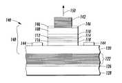
- a first distributed Bragg reflector 122is formed over the p-contact layer 120 .
- the first distributed Bragg reflector 122has six pairs of quarter-wavelength thick alternating silicon dioxide (SiO 2 ) and tantalum pentoxide (Ta 2 O 5 ) dielectric layers.
- the DBRcan have alternating layers of SiO 2 /TiO 2 or GaN/AlGaN or alternating layers of AlGaN with different aluminum content.
- the DBRcan have more or less than six pairs of alternating layers, if higher reflectivity is desired. However, fewer number of pairs may be desired in the case of photodetectors in order to enhance light extraction.
- a gold Au layer 124is formed over the first distributed Bragg reflector 122 .
- the gold overlayer 124has a typical thickness of 20 to 200 ⁇ m.
- the upper surface 126 of the gold overlayer 124is bonded to a silicon (Si) substrate 128 using an adhesive bond 130 .
- the adhesive 124may be a cyanoacrylate-based glue.
- the support substratecould alternatively be gallium arsenide (GaAs), copper or any rigid material.
- the adhesivecould alternately be a thin film adhesive, spin-on glass, or any appropriate solder.
- the use of copper or other metals as the support substrate 128 bonded to the gold layer 124provides good thermal conductivity.
- the lower surface 132 of the sapphire substrate 100is polished to a very smooth surface finish to minimize light scattering. Polishing is accomplished mechanically using a succession of diamond pads (not shown). During the polishing procedure, the diamond grit size is gradually reduced from a grit size of about 30 ⁇ m down to a grit size of 0.1 ⁇ m. Typical root mean square (rms) roughness after polishing is about 20-50 Angstrom. Polishing may be done before bonding to the support substrate.
- an ultraviolet excimer laser 134then emits a laser beam 136 which is transmitted through the sapphire substrate 100 to the interface 138 between the GaN buffer layer 104 and the laser absorption InGaN layer 106 .
- Sapphire and gallium nitrideare transparent to the wavelength of the light beam emitted by the laser. Proper adjustment of the excimer laser allows decomposition of the thin laser absorption InGaN layer 106 at the interface 138 between the GaN buffer layer 104 and the sacrificial InGaN layer 106 .
- the InGaN layer 106is decomposed into indium and gallium metal and gaseous nitrogen by the radiation from the laser beam through the sapphire substrate and the gallium nitride layer.
- the InGaN layer 106is a laser absorption layer with the wavelength of the light beam 136 matching the decomposition of the indium.
- a homogenizer(not-shown) converts the Gaussian-profile beam emitted by the laser to a flat plateau-like laser beam which provides improved beam uniformity.
- a larger surface area of the laser absorption InGaN layermay be exposed by scanning the laser beam across the interface surface rather than providing a stationary beam.
- the excimer laseris typically pulsed in the range of 5-10 Hz with one pulse typically being. sufficient to achieve decomposition of the GaN layer.
- the polished lower surface 132 of the sapphire substrate 100allows uniform excimer laser exposure of the InGaN layer 106 .
- any residual indium or gallium metal on the surface 142 of the GaN contact layer 108is removed with a hydrochloric acid (HCL) and water solution dip (HCL:H 2 O ⁇ 1:1).
- HCLhydrochloric acid
- H 2 O ⁇ 1:1water solution dip
- the sapphire substrate 100is reusable for subsequent fabrication of nitride based semiconductor structures.
- the substrate 100need not be sapphire but can be any optically transparent material which is transmissive to the wavelength of the light beam 136 from,the laser 134 and suitable for growth of GaN layers on its surface.
- the semiconductor structure 140is then inverted with the silicon (Si) substrate 128 and the p-doped layers down and the n-contact layer 108 on top of the inverted laser structure.
- Dry-etching using CAIBE (chemical assisted ion beam etching) or RIE (reactive ion beam etching) in an Ar/Cl 2 /BCl 3 gas mixtureis used to etch the semiconductor structure 140 through the n-contact layer 108 , the n-cladding layer 110 , the n-waveguide layer 112 , the InGaN active region 114 , the p-wave guide layer 116 , the p-cladding layer 118 down to expose the GaN:Mg current-spreading and p-contact layer 120 .
- a second distributed Bragg reflector 142is formed over the central portion of the n-contact layer 108 .
- the second distributed Bragg reflector 142has six pairs of quarter-wavelength thick alternating silicon dioxide (SiO 2 ) and tantalum pentoxide (Ta 2 O 5 ) dielectric layers.
- the DBRcan have alternating layers of SiO 2 /TiO 2 or GaN/AIGaN or alternating layers of GaN with different aluminum content.
- the DBRcan have more or less than six pairs of alternating layers, depending upon the specific device.
- a p-type Ni/Au electrode 144is formed on the etched, exposed p-current-spreading layer 120 of the semiconductor structure 140 , which is functioning as a lateral contact layer.
- An n-type Ti/Al electrode 146is formed on the exposed n-contact layer 118 of the semiconductor structure 140 , surrounding the second DBR 142 .
- the resonant cavity 148 of the semiconductor structure 140 between the first DBR 122 and the second DBR 142consists of the n-contact layer 108 , the n-cladding layer 110 , the n-waveguide layer 112 , the InGaN active region 114 , the p-waveguide layer 116 , the p-cladding layer 118 , and the p-contact layer 120 .
- the nitride based resonant cavity semiconductor structure 140can be either a vertical cavity surface emitting laser (VCSEL), a light emitting diode (LED, or a photodetector (PD), or a combination of these devices.
- VCSELvertical cavity surface emitting laser
- LEDlight emitting diode
- PDphotodetector
- the semiconductor structure 140is a VCSEL
- the first DBR 122 and the second DBR 142are highly reflective by increasing. the number of high refractive index/low refractive index semiconductor or dielectric layer. pairs and/or increasing the difference between the high refractive index and low refractive index.
- a forward biased electrical potentialis applied between the p-electrode 144 and the n-electrode 146 causing emission of light from the active region 114 which is amplified in the. resonant cavity 148 by continuous reflection between the two DBRs 122 and 142 before emission of coherent light 150 through the second DBR 142 of the VCSEL structure 140 .
- the second DBR 142is less reflective than those of a VCSEL by decreasing number of high refractive index/low refractive index dielectric or semiconductor layer pairs and/or decreasing the difference between the high refractive index and low refractive index.
- a forward biased electrical potentialis applied between the p-electrode 144 and the n-electrode 146 causing emission of light 150 from the active region 114 in the resonant cavity 148 through the second DBR 142 of the LED structure 140 .
- the semiconductor structure 140is a photodetector, then the second DBR 142 is less reflective than those of a VCSEL by decreasing number of high refractive index/low refractive index dielectric or semiconductor layer pairs and/or decreasing the difference between the high refractive index and low refractive index.
- a reverse biased electrical potentialis applied between the p-electrode 144 and the n-electrode 146 causing absorption of light 150 in the active region 114 in the resonant cavity 148 through the second DBR 142 of the LED structure 140 .
- the absorptionwill produce a photocurrent.
- the nitride based resonant cavity semiconductor structurecan be fabricated with the p-doped semiconductor layers up by removing the epitaxial layer host layer after forming the second DBR, then transfer to a support substrate.
- the laser assisted epitaxial lift-off of the sapphire substrate and then the inversion of the semiconductor structurewill form the more traditional n-side down, p-side up semiconductor structure.
- a gold thin layercan be deposited on the second DBR and a thick metal, such as copper, can be plated to form the support substrate.
- the nitride based resonant cavity semiconductor structurecan emit light from the VCSEL or LED or absorb light from the photodetector if the substrate is transparent to the wavelength of light emitted or absorbed and the lower DBR has less reflectivity than the upper DBR.
- the use of laser-assisted epitaxial lift-off of the first sapphire substrateallows access to the backside of nitride based semiconductor layers for the fabrication of distributed Bragg reflectors on both sides of the nitride based resonant cavity semiconductor structure.
- An integrated nitride based resonant cavity semiconductor structurescan be fabricated with a VCSEL and a photodetector, or a LED and a photodetector, or a VCSEL and a LED, or with a VCSEL, LED and a photodetector.
Landscapes
- Physics & Mathematics (AREA)
- Optics & Photonics (AREA)
- Chemical & Material Sciences (AREA)
- Engineering & Computer Science (AREA)
- Nanotechnology (AREA)
- Condensed Matter Physics & Semiconductors (AREA)
- General Physics & Mathematics (AREA)
- Electromagnetism (AREA)
- Life Sciences & Earth Sciences (AREA)
- Biophysics (AREA)
- Crystallography & Structural Chemistry (AREA)
- Semiconductor Lasers (AREA)
Abstract
Description
Claims (15)
Priority Applications (8)
| Application Number | Priority Date | Filing Date | Title |
|---|---|---|---|
| US10/024,236US6455340B1 (en) | 2001-12-21 | 2001-12-21 | Method of fabricating GaN semiconductor structures using laser-assisted epitaxial liftoff |
| DE60236402TDE60236402D1 (en) | 2001-12-21 | 2002-12-12 | Method for producing semiconductor devices |
| EP02258579AEP1326290B1 (en) | 2001-12-21 | 2002-12-12 | Method of fabricating semiconductor structures |
| CA002414325ACA2414325C (en) | 2001-12-21 | 2002-12-13 | Method of fabricating gan semiconductor structures using laser-assisted epitaxial liftoff |
| JP2002364556AJP2003234542A (en) | 2001-12-21 | 2002-12-17 | Method for manufacturing nitride-based resonator semiconductor structure |
| BR0205196-6ABR0205196A (en) | 2001-12-21 | 2002-12-19 | Manufacturing Process of Gan Semiconductor Structures Using Laser Assisted Epitaxial Dislocation |
| BRPI0205196-6ABRPI0205196B1 (en) | 2001-12-21 | 2002-12-19 | METHOD FOR PRODUCING A NITRECT RESONANT CABITY SEMICONDUCTOR STRUCTURE |
| JP2010149348AJP2010212738A (en) | 2001-12-21 | 2010-06-30 | Method of fabricating nitride-based resonator semiconductor structure |
Applications Claiming Priority (1)
| Application Number | Priority Date | Filing Date | Title |
|---|---|---|---|
| US10/024,236US6455340B1 (en) | 2001-12-21 | 2001-12-21 | Method of fabricating GaN semiconductor structures using laser-assisted epitaxial liftoff |
Publications (1)
| Publication Number | Publication Date |
|---|---|
| US6455340B1true US6455340B1 (en) | 2002-09-24 |
Family
ID=21819551
Family Applications (1)
| Application Number | Title | Priority Date | Filing Date |
|---|---|---|---|
| US10/024,236Expired - LifetimeUS6455340B1 (en) | 2001-12-21 | 2001-12-21 | Method of fabricating GaN semiconductor structures using laser-assisted epitaxial liftoff |
Country Status (6)
| Country | Link |
|---|---|
| US (1) | US6455340B1 (en) |
| EP (1) | EP1326290B1 (en) |
| JP (2) | JP2003234542A (en) |
| BR (2) | BRPI0205196B1 (en) |
| CA (1) | CA2414325C (en) |
| DE (1) | DE60236402D1 (en) |
Cited By (103)
| Publication number | Priority date | Publication date | Assignee | Title |
|---|---|---|---|---|
| US20030160257A1 (en)* | 2002-02-26 | 2003-08-28 | Stefan Bader | Radiation-emitting semiconductor component with a vertical emission direction and fabrication method for producing the semiconductor component |
| US20030189212A1 (en)* | 2002-04-09 | 2003-10-09 | Yoo Myung Cheol | Method of fabricating vertical devices using a metal support film |
| US20030223756A1 (en)* | 2002-06-04 | 2003-12-04 | Honeywell International Inc. | Optical transceiver |
| US20030231683A1 (en)* | 2002-05-30 | 2003-12-18 | Xerox Corporation | Nitride based semiconductor structures with highly reflective mirrors |
| US6711194B2 (en)* | 2001-02-08 | 2004-03-23 | The Furukawa Electric Co., Ltd. | High output power semiconductor laser diode |
| US20040061433A1 (en)* | 2001-10-12 | 2004-04-01 | Nichia Corporation, Corporation Of Japan | Light emitting apparatus and method of manufacturing the same |
| US20040072383A1 (en)* | 2002-07-08 | 2004-04-15 | Nichia Corporation | Nitride semiconductor device comprising bonded substrate and fabrication method of the same |
| US6813295B2 (en)* | 2002-03-25 | 2004-11-02 | Agilent Technologies, Inc. | Asymmetric InGaAsN vertical cavity surface emitting lasers |
| US20040245543A1 (en)* | 2003-06-04 | 2004-12-09 | Yoo Myung Cheol | Method of fabricating vertical structure compound semiconductor devices |
| US20050012113A1 (en)* | 2003-07-17 | 2005-01-20 | Jinn-Kong Sheu | [uv photodetector] |
| US20050029539A1 (en)* | 2002-03-26 | 2005-02-10 | Sanyo Electric Co., Ltd. | Nitride-based semiconductor device and method of fabricating the same |
| US6869812B1 (en)* | 2003-05-13 | 2005-03-22 | Heng Liu | High power AllnGaN based multi-chip light emitting diode |
| US20050087884A1 (en)* | 2003-10-24 | 2005-04-28 | Stokes Edward B. | Flip-chip light emitting diode |
| US20050117623A1 (en)* | 2003-12-01 | 2005-06-02 | Nl-Nanosemiconductor Gmbh | Optoelectronic device incorporating an interference filter |
| EP1555732A2 (en) | 2004-01-19 | 2005-07-20 | Lg Electronics Inc. | Nitride semiconductor laser diode and method for manufacturing the same |
| US20050173724A1 (en)* | 2004-02-11 | 2005-08-11 | Heng Liu | Group III-nitride based LED having a transparent current spreading layer |
| US6934312B2 (en)* | 2002-09-30 | 2005-08-23 | Agilent Technologies, Inc. | System and method for fabricating efficient semiconductor lasers via use of precursors having a direct bond between a group III atom and a nitrogen atom |
| US20050242365A1 (en)* | 2004-04-28 | 2005-11-03 | Yoo Myung C | Vertical structure semiconductor devices |
| US20050247950A1 (en)* | 2004-05-06 | 2005-11-10 | Cree, Inc. | Lift-off process for GaN films formed on SiC substrates and devices fabricated using the method |
| WO2005106972A1 (en)* | 2004-04-29 | 2005-11-10 | Osram Opto Semiconductors Gmbh | Method for production a radiation-emitting semi-conductor chip |
| US6969874B1 (en)* | 2003-06-12 | 2005-11-29 | Sandia Corporation | Flip-chip light emitting diode with resonant optical microcavity |
| US20050271092A1 (en)* | 2004-06-07 | 2005-12-08 | Nl-Nanosemiconductor Gmbh | Electrooptically wavelength-tunable resonant cavity optoelectronic device for high-speed data transfer |
| US20050274971A1 (en)* | 2004-06-10 | 2005-12-15 | Pai-Hsiang Wang | Light emitting diode and method of making the same |
| US20050286590A1 (en)* | 2004-06-25 | 2005-12-29 | Samsung Electro-Mechanics Co., Ltd. | Method of producing multi-wavelength semiconductor laser device |
| US20050286591A1 (en)* | 2004-06-25 | 2005-12-29 | Samsung Electro-Mechanics Co., Ltd. | Method of producing multi-wavelength semiconductor laser device |
| US20060006554A1 (en)* | 2004-06-22 | 2006-01-12 | Yoo Myung C | Vertical structure semiconductor devices with improved light output |
| US20060054919A1 (en)* | 2004-08-27 | 2006-03-16 | Kyocera Corporation | Light-emitting element, method for manufacturing the same and lighting equipment using the same |
| US20060105542A1 (en)* | 2004-11-15 | 2006-05-18 | Yoo Myung C | Method for fabricating and separating semiconductor devices |
| US20060228901A1 (en)* | 2003-07-08 | 2006-10-12 | Seoul National University Industry Foundation | Growth method for nitride semiconductor epitaxial layers |
| US20060225644A1 (en)* | 2005-04-07 | 2006-10-12 | Samsung Electro-Mechanics Co.,Ltd. | Vertical group III-nitride light emitting device and method for manufacturing the same |
| JP2006523953A (en)* | 2003-04-15 | 2006-10-19 | ルミナス ディバイシズ インコーポレイテッド | Light emitting element |
| US20060243991A1 (en)* | 2004-12-29 | 2006-11-02 | Cheng-Yi Liu | Light emitting diode and manufacturing method thereof |
| US20060255349A1 (en)* | 2004-05-11 | 2006-11-16 | Heng Liu | High power AllnGaN based multi-chip light emitting diode |
| US20070081570A1 (en)* | 2005-10-12 | 2007-04-12 | Samsung Electronics Co., Ltd. | Side light emitting type semiconductor laser diode having dielectric layer formed on active layer |
| US20070105260A1 (en)* | 2005-11-08 | 2007-05-10 | Sharp Kabushiki Kaisha | Nitride-based semiconductor device and production method thereof |
| US20070108456A1 (en)* | 2005-11-14 | 2007-05-17 | Palo Alto Research Center Incorporated | Superlattice strain relief layer for semiconductor devices |
| US20070111345A1 (en)* | 2005-11-14 | 2007-05-17 | Palo Alto Research Center Incorporated | Method for controlling the structure and surface qualities of a thin film and product produced thereby |
| US20070145380A1 (en)* | 2006-05-19 | 2007-06-28 | Shum Frank T | Low optical loss electrode structures for LEDs |
| US20070206488A1 (en)* | 2006-02-23 | 2007-09-06 | Claes Thelander | Data storage nanostructures |
| US20070221944A1 (en)* | 2005-11-15 | 2007-09-27 | Myung Cheol Yoo | Light emitting diodes and fabrication methods thereof |
| US20070298587A1 (en)* | 2004-03-29 | 2007-12-27 | J.P. Sercel Associates Inc. | Method of separating layers of material |
| CN100361355C (en)* | 2002-11-19 | 2008-01-09 | Jds尤尼弗思公司 | Low Voltage Multijunction Vertical Cavity Surface Emitting Laser |
| US20080054248A1 (en)* | 2006-09-06 | 2008-03-06 | Chua Christopher L | Variable period variable composition supperlattice and devices including same |
| US20080149944A1 (en)* | 2006-12-22 | 2008-06-26 | Qunano Ab | Led with upstanding nanowire structure and method of producing such |
| US20080149914A1 (en)* | 2006-12-22 | 2008-06-26 | Qunano Ab | Nanoelectronic structure and method of producing such |
| WO2008079078A1 (en)* | 2006-12-22 | 2008-07-03 | Qunano Ab | Elevated led and method of producing such |
| WO2008079076A1 (en)* | 2006-12-22 | 2008-07-03 | Qunano Ab | Led with upstanding nanowire structure and method of producing such |
| US20080179605A1 (en)* | 2007-01-29 | 2008-07-31 | Yuji Takase | Nitride semiconductor light emitting device and method for fabricating the same |
| WO2008065607A3 (en)* | 2006-11-30 | 2008-08-07 | Philips Intellectual Property | Intrinsic flux sensing |
| US20080197367A1 (en)* | 2007-02-16 | 2008-08-21 | Hong Kong Applied Science And Technology Research Institute Co. Ltd. | Method of super flat chemical mechanical polishing technology and semiconductor elements produced thereof |
| US20080197369A1 (en)* | 2007-02-20 | 2008-08-21 | Cree, Inc. | Double flip semiconductor device and method for fabrication |
| GB2447091A (en)* | 2007-03-02 | 2008-09-03 | James Stuart Mckenzie | Vertical LED |
| US20080261378A1 (en)* | 2005-04-04 | 2008-10-23 | Tohoku Techno Arch Co., Ltd. | Method for Growth of Gan Single Crystal, Method for Preparation of Gan Substrate, Process for Producing Gan-Based Element, and Gan-Based Element |
| CN100452328C (en)* | 2003-09-19 | 2009-01-14 | 霆激技术有限公司 | Fabrication of Conductive Metal Layers on Semiconductor Devices |
| WO2009015192A1 (en)* | 2007-07-23 | 2009-01-29 | Photronix, Inc. | Methods for growing selective areas on substrates and devices thereof |
| US20090053845A1 (en)* | 2005-11-14 | 2009-02-26 | Palo Alto Research Center Incorporated | Method For Controlling The Structure And Surface Qualities Of A Thin Film And Product Produced Thereby |
| US20090050911A1 (en)* | 2007-08-24 | 2009-02-26 | Cree, Inc. | Light emitting device packages using light scattering particles of different size |
| US20090050903A1 (en)* | 2007-08-21 | 2009-02-26 | Cree, Inc. | Selective wet etching of gold-tin based solder |
| US20090152573A1 (en)* | 2007-12-14 | 2009-06-18 | Cree, Inc. | Textured encapsulant surface in LED packages |
| US20090206361A1 (en)* | 2006-03-24 | 2009-08-20 | Showa Denko K.K., | Group iii nitride semiconductor light emitting device, method for producing the same, and lamp thereof |
| US20090321775A1 (en)* | 2008-06-26 | 2009-12-31 | Ghulam Hasnain | LED with Reduced Electrode Area |
| US20100032701A1 (en)* | 2008-08-05 | 2010-02-11 | Sharp Kabushiki Kaisha | Nitride semiconductor light emitting device and method of manufacturing the same |
| US20100098127A1 (en)* | 2008-10-22 | 2010-04-22 | Nichia Corporation | Method of manufacturing nitride semiconductor light emitting element and nitride semiconductor light emitting element |
| US20100163911A1 (en)* | 2006-05-19 | 2010-07-01 | Shum Frank T | Electrode structures for leds with increased active area |
| US20100166032A1 (en)* | 2007-12-17 | 2010-07-01 | Palo Alto Research Center Incorporated | Buried Aperture Nitride Light-Emiting Device |
| US20100171125A1 (en)* | 2002-06-26 | 2010-07-08 | Yoo Myung Cheol | Thin film light emitting diode |
| US20110037051A1 (en)* | 2007-08-10 | 2011-02-17 | Hong Kong Applied Science and Technology Research Institute Company Limited | Optimization of polishing stop design |
| CN1937271B (en)* | 2005-09-22 | 2011-03-09 | 三洋电机株式会社 | Method of manufacturing nitride semiconductor device |
| US20110136324A1 (en)* | 2009-12-09 | 2011-06-09 | Cooledge Lighting, Inc. | Semiconductor dice transfer-enabling apparatus and method for manufacturing transfer-enabling apparatus |
| US20110132549A1 (en)* | 2009-12-07 | 2011-06-09 | J.P. Sercel Associates, Inc. | Laser lift off systems and methods |
| US20110134954A1 (en)* | 2009-12-07 | 2011-06-09 | Letertre Fabrice M | SEMICONDUCTOR DEVICE HAVING AN InGaN LAYER |
| US20110151588A1 (en)* | 2009-12-17 | 2011-06-23 | Cooledge Lighting, Inc. | Method and magnetic transfer stamp for transferring semiconductor dice using magnetic transfer printing techniques |
| US20110151602A1 (en)* | 2009-12-18 | 2011-06-23 | Cooledge Lighting, Inc. | Method of manufacturing transferable elements incorporating radiation enabled lift off for allowing transfer from host substrate |
| CN102203966A (en)* | 2008-10-28 | 2011-09-28 | 松下电工株式会社 | Method for manufacturing semiconductor light-emitting element |
| US8050728B2 (en) | 2005-03-01 | 2011-11-01 | Masimo Laboratories, Inc. | Multiple wavelength sensor drivers |
| US8222064B2 (en) | 2007-08-10 | 2012-07-17 | Hong Kong Applied Science and Technology Research Institute Company Limited | Vertical light emitting diode device structure and method of fabricating the same |
| US20120241821A1 (en)* | 2009-12-01 | 2012-09-27 | Soitec | Heterostructure for electronic power components, optoelectronic or photovoltaic components |
| US8368118B2 (en) | 2008-12-16 | 2013-02-05 | Hewlett-Packard Development Company, L.P. | Semiconductor structure having an ELOG on a thermally and electrically conductive mask |
| US8513643B2 (en) | 2006-09-06 | 2013-08-20 | Palo Alto Research Center Incorporated | Mixed alloy defect redirection region and devices including same |
| CN103325894A (en)* | 2013-07-04 | 2013-09-25 | 厦门大学 | Manufacturing method of electrically injected GaN-based resonant cavity |
| US20140027806A1 (en)* | 2009-07-15 | 2014-01-30 | Shih-Cheng Huang | Semiconductor optoelectronic structure with increased light extraction efficiency |
| US8693894B2 (en) | 2008-04-28 | 2014-04-08 | Hewlett-Packard Development Company, L.P. | Gain clamped optical device for emitting LED mode light |
| CN103904015A (en)* | 2014-03-21 | 2014-07-02 | 中国电子科技集团公司第五十五研究所 | Method for stripping and transferring gallium arsenide based epitaxial layer |
| US8781544B2 (en) | 2007-03-27 | 2014-07-15 | Cercacor Laboratories, Inc. | Multiple wavelength optical sensor |
| US8801613B2 (en) | 2009-12-04 | 2014-08-12 | Masimo Corporation | Calibration for multi-stage physiological monitors |
| US20140231839A1 (en)* | 2012-07-18 | 2014-08-21 | Semicon Light Co., Ltd. | Semiconductor Light Emitting Device |
| US8965471B2 (en) | 2007-04-21 | 2015-02-24 | Cercacor Laboratories, Inc. | Tissue profile wellness monitor |
| US9056424B2 (en) | 2012-12-20 | 2015-06-16 | Samsung Electronics Co., Ltd. | Methods of transferring graphene and manufacturing device using the same |
| RU2576589C2 (en)* | 2009-12-23 | 2016-03-10 | Таль | Compact thermoelastic waveguide actuator, waveguide with phase stability and multiplexer with such actuator |
| CN105655387A (en)* | 2016-03-23 | 2016-06-08 | 安徽三安光电有限公司 | Semiconductor epitaxial wafer and preparation method thereof |
| US9669613B2 (en) | 2010-12-07 | 2017-06-06 | Ipg Photonics Corporation | Laser lift off systems and methods that overlap irradiation zones to provide multiple pulses of laser irradiation per location at an interface between layers to be separated |
| US9839381B1 (en) | 2009-11-24 | 2017-12-12 | Cercacor Laboratories, Inc. | Physiological measurement system with automatic wavelength adjustment |
| US10658998B2 (en) | 2013-07-31 | 2020-05-19 | Oepic Semiconductors, Inc. | Piezoelectric film transfer for acoustic resonators and filters |
| CN111725368A (en)* | 2020-06-30 | 2020-09-29 | 中南大学 | A GaN-based vertical structure micro-cavity Micro-LED based on electroplating technology and its preparation method |
| CN111755563A (en)* | 2020-05-26 | 2020-10-09 | 晶澳(扬州)太阳能科技有限公司 | A kind of P-type single crystal silicon boron back field double-sided battery and preparation method thereof |
| WO2021221894A1 (en)* | 2020-04-27 | 2021-11-04 | Apple Inc. | An integrated vertical emitter structure having controlled wavelength |
| US11309453B2 (en) | 2017-01-16 | 2022-04-19 | Apple Inc. | Combining light-emitting elements of differing divergence on the same substrate |
| US11322910B2 (en) | 2019-02-21 | 2022-05-03 | Apple Inc. | Indium-phosphide VCSEL with dielectric DBR |
| US11374381B1 (en) | 2019-06-10 | 2022-06-28 | Apple Inc. | Integrated laser module |
| US11381060B2 (en) | 2017-04-04 | 2022-07-05 | Apple Inc. | VCSELs with improved optical and electrical confinement |
| US11418010B2 (en) | 2019-04-01 | 2022-08-16 | Apple Inc. | VCSEL array with tight pitch and high efficiency |
| US20220393436A1 (en)* | 2021-06-07 | 2022-12-08 | Stanley Electric Co., Ltd. | Vertical cavity light-emitting element and manufacturing method of the same |
| US12029586B2 (en) | 2006-10-12 | 2024-07-09 | Masimo Corporation | Oximeter probe off indicator defining probe off space |
Families Citing this family (17)
| Publication number | Priority date | Publication date | Assignee | Title |
|---|---|---|---|---|
| JP2007521635A (en)* | 2003-09-19 | 2007-08-02 | ティンギ テクノロジーズ プライベート リミテッド | Semiconductor device manufacturing |
| KR20070013273A (en) | 2004-03-15 | 2007-01-30 | 팅기 테크놀러지스 프라이빗 리미티드 | Fabrication of Semiconductor Devices |
| EP1756875A4 (en) | 2004-04-07 | 2010-12-29 | Tinggi Technologies Private Ltd | FABRICATION OF A RETROFLECTIVE LAYER ON SEMICONDUCTOR ELECTROLUMINESCENT DIODES |
| SG130975A1 (en) | 2005-09-29 | 2007-04-26 | Tinggi Tech Private Ltd | Fabrication of semiconductor devices for light emission |
| SG131803A1 (en) | 2005-10-19 | 2007-05-28 | Tinggi Tech Private Ltd | Fabrication of transistors |
| SG133432A1 (en) | 2005-12-20 | 2007-07-30 | Tinggi Tech Private Ltd | Localized annealing during semiconductor device fabrication |
| JP4804930B2 (en)* | 2006-01-23 | 2011-11-02 | ローム株式会社 | Method of manufacturing nitride semiconductor device |
| SG140473A1 (en) | 2006-08-16 | 2008-03-28 | Tinggi Tech Private Ltd | Improvements in external light efficiency of light emitting diodes |
| SG140512A1 (en) | 2006-09-04 | 2008-03-28 | Tinggi Tech Private Ltd | Electrical current distribution in light emitting devices |
| US8102045B2 (en) | 2007-08-08 | 2012-01-24 | Infineon Technologies Ag | Integrated circuit with galvanically bonded heat sink |
| DE102007046519A1 (en)* | 2007-09-28 | 2009-04-02 | Osram Opto Semiconductors Gmbh | Thin-film LED with a mirror layer and method for its production |
| KR100949571B1 (en)* | 2008-01-21 | 2010-03-25 | 포항공과대학교 산학협력단 | Photon laser and its manufacturing method |
| JP5002703B2 (en) | 2010-12-08 | 2012-08-15 | 株式会社東芝 | Semiconductor light emitting device |
| CN102820389B (en)* | 2012-07-21 | 2015-11-25 | 张�杰 | A kind of inverted structure light-emitting diode based on ELO technology and preparation method thereof |
| JP2014041964A (en)* | 2012-08-23 | 2014-03-06 | Sharp Corp | Method of manufacturing nitride semiconductor light-emitting element, and nitride semiconductor light-emitting element |
| FR3009644B1 (en)* | 2013-08-08 | 2016-12-23 | Soitec Silicon On Insulator | METHOD, STACK AND ASSEMBLY FOR SEPARATING A STRUCTURE OF A SUBSTRATE BY ELECTROMAGNETIC IRRADIATION |
| WO2023072408A1 (en)* | 2021-10-29 | 2023-05-04 | Ams-Osram International Gmbh | Otpoelectronic device and method for processing the same |
Citations (7)
| Publication number | Priority date | Publication date | Assignee | Title |
|---|---|---|---|---|
| US5838707A (en)* | 1996-12-27 | 1998-11-17 | Motorola, Inc. | Ultraviolet/visible light emitting vertical cavity surface emitting laser and method of fabrication |
| US5972730A (en)* | 1996-09-26 | 1999-10-26 | Kabushiki Kaisha Toshiba | Nitride based compound semiconductor light emitting device and method for producing the same |
| US5978401A (en) | 1995-10-25 | 1999-11-02 | Honeywell Inc. | Monolithic vertical cavity surface emitting laser and resonant cavity photodetector transceiver |
| JP2000022282A (en)* | 1998-07-02 | 2000-01-21 | Fuji Xerox Co Ltd | Surface light-emitting-type light-emitting device and its manufacture |
| US6046065A (en)* | 1996-09-13 | 2000-04-04 | Alcatel | Process for fabricating a semiconductor opto-electronic component and component and matrix of components fabricated by this process |
| US6148016A (en) | 1997-11-06 | 2000-11-14 | The Regents Of The University Of California | Integrated semiconductor lasers and photodetectors |
| US6376269B1 (en)* | 1999-02-02 | 2002-04-23 | Agilent Technologies, Inc. | Vertical cavity surface emitting laser (VCSEL) using buried Bragg reflectors and method for producing same |
Family Cites Families (12)
| Publication number | Priority date | Publication date | Assignee | Title |
|---|---|---|---|---|
| JP3093547B2 (en)* | 1993-12-28 | 2000-10-03 | 日本電気株式会社 | Optical integrated circuit and method of manufacturing the same |
| JP3511970B2 (en)* | 1995-06-15 | 2004-03-29 | 日亜化学工業株式会社 | Nitride semiconductor light emitting device |
| US5877519A (en)* | 1997-03-26 | 1999-03-02 | Picolight Incoporated | Extended wavelength opto-electronic devices |
| JPH11154774A (en)* | 1997-08-05 | 1999-06-08 | Canon Inc | Method for manufacturing surface-emitting semiconductor device, surface-emitting semiconductor device manufactured by this method, and display device using this device |
| JP4043087B2 (en)* | 1998-01-23 | 2008-02-06 | 日亜化学工業株式会社 | Nitride semiconductor device manufacturing method and nitride semiconductor device |
| JP3559453B2 (en)* | 1998-06-29 | 2004-09-02 | 株式会社東芝 | Light emitting element |
| JP3316479B2 (en)* | 1998-07-29 | 2002-08-19 | 三洋電機株式会社 | Semiconductor device, semiconductor light emitting device, and method of manufacturing semiconductor device |
| JP3525061B2 (en)* | 1998-09-25 | 2004-05-10 | 株式会社東芝 | Method for manufacturing semiconductor light emitting device |
| US20010042866A1 (en)* | 1999-02-05 | 2001-11-22 | Carrie Carter Coman | Inxalygazn optical emitters fabricated via substrate removal |
| US6320206B1 (en)* | 1999-02-05 | 2001-11-20 | Lumileds Lighting, U.S., Llc | Light emitting devices having wafer bonded aluminum gallium indium nitride structures and mirror stacks |
| JP4529215B2 (en)* | 1999-10-29 | 2010-08-25 | 日亜化学工業株式会社 | Nitride semiconductor growth method |
| JP4204163B2 (en)* | 2000-02-03 | 2009-01-07 | 株式会社リコー | Manufacturing method of semiconductor substrate |
- 2001
- 2001-12-21USUS10/024,236patent/US6455340B1/ennot_activeExpired - Lifetime
- 2002
- 2002-12-12DEDE60236402Tpatent/DE60236402D1/ennot_activeExpired - Lifetime
- 2002-12-12EPEP02258579Apatent/EP1326290B1/ennot_activeExpired - Lifetime
- 2002-12-13CACA002414325Apatent/CA2414325C/ennot_activeExpired - Fee Related
- 2002-12-17JPJP2002364556Apatent/JP2003234542A/enactivePending
- 2002-12-19BRBRPI0205196-6Apatent/BRPI0205196B1/enunknown
- 2002-12-19BRBR0205196-6Apatent/BR0205196A/enactiveIP Right Grant
- 2010
- 2010-06-30JPJP2010149348Apatent/JP2010212738A/enactivePending
Patent Citations (7)
| Publication number | Priority date | Publication date | Assignee | Title |
|---|---|---|---|---|
| US5978401A (en) | 1995-10-25 | 1999-11-02 | Honeywell Inc. | Monolithic vertical cavity surface emitting laser and resonant cavity photodetector transceiver |
| US6046065A (en)* | 1996-09-13 | 2000-04-04 | Alcatel | Process for fabricating a semiconductor opto-electronic component and component and matrix of components fabricated by this process |
| US5972730A (en)* | 1996-09-26 | 1999-10-26 | Kabushiki Kaisha Toshiba | Nitride based compound semiconductor light emitting device and method for producing the same |
| US5838707A (en)* | 1996-12-27 | 1998-11-17 | Motorola, Inc. | Ultraviolet/visible light emitting vertical cavity surface emitting laser and method of fabrication |
| US6148016A (en) | 1997-11-06 | 2000-11-14 | The Regents Of The University Of California | Integrated semiconductor lasers and photodetectors |
| JP2000022282A (en)* | 1998-07-02 | 2000-01-21 | Fuji Xerox Co Ltd | Surface light-emitting-type light-emitting device and its manufacture |
| US6376269B1 (en)* | 1999-02-02 | 2002-04-23 | Agilent Technologies, Inc. | Vertical cavity surface emitting laser (VCSEL) using buried Bragg reflectors and method for producing same |
Cited By (300)
| Publication number | Priority date | Publication date | Assignee | Title |
|---|---|---|---|---|
| US6711194B2 (en)* | 2001-02-08 | 2004-03-23 | The Furukawa Electric Co., Ltd. | High output power semiconductor laser diode |
| US7301175B2 (en) | 2001-10-12 | 2007-11-27 | Nichia Corporation | Light emitting apparatus and method of manufacturing the same |
| US20060267042A1 (en)* | 2001-10-12 | 2006-11-30 | Nichia Corporation | Light emitting apparatus and method of manufacturing the same |
| US7390684B2 (en) | 2001-10-12 | 2008-06-24 | Nichia Corporation | Light emitting apparatus and method of manufacturing the same |
| US20040061433A1 (en)* | 2001-10-12 | 2004-04-01 | Nichia Corporation, Corporation Of Japan | Light emitting apparatus and method of manufacturing the same |
| US20030160257A1 (en)* | 2002-02-26 | 2003-08-28 | Stefan Bader | Radiation-emitting semiconductor component with a vertical emission direction and fabrication method for producing the semiconductor component |
| US6813295B2 (en)* | 2002-03-25 | 2004-11-02 | Agilent Technologies, Inc. | Asymmetric InGaAsN vertical cavity surface emitting lasers |
| US20080179601A1 (en)* | 2002-03-26 | 2008-07-31 | Tadao Toda | Nitride-based semiconductor device and method of fabricating the same |
| US20080067541A1 (en)* | 2002-03-26 | 2008-03-20 | Tadao Toda | Nitride-based semiconductor device and method of fabricating the same |
| US20080069162A1 (en)* | 2002-03-26 | 2008-03-20 | Tadao Toda | Nitride-based semiconductor device and method of fabricating the same |
| US20050191775A1 (en)* | 2002-03-26 | 2005-09-01 | Sanyo Electric Co., Ltd. | Nitride-based semiconductor device and method of fabricating the same |
| US20050029539A1 (en)* | 2002-03-26 | 2005-02-10 | Sanyo Electric Co., Ltd. | Nitride-based semiconductor device and method of fabricating the same |
| US7629623B2 (en) | 2002-03-26 | 2009-12-08 | Sanyo Electric Co., Ltd. | Nitride-based semiconductor device and method of fabricating the same |
| US6890779B2 (en)* | 2002-03-26 | 2005-05-10 | Sanyo Electric Co., Ltd. | Nitride-based semiconductor device and method of fabricating the same |
| US7655484B2 (en) | 2002-03-26 | 2010-02-02 | Sanyo Electric Co., Ltd. | Nitride-based semiconductor device and method of fabricating the same |
| US20090072264A1 (en)* | 2002-04-09 | 2009-03-19 | Yoo Myung Cheol | Method of fabricating vertical Devices using a metal support film |
| US8022386B2 (en)* | 2002-04-09 | 2011-09-20 | Lg Electronics Inc. | Vertical topology light emitting device |
| US9847455B2 (en) | 2002-04-09 | 2017-12-19 | Lg Innotek Co., Ltd. | Vertical topology light emitting device |
| US9209360B2 (en) | 2002-04-09 | 2015-12-08 | Lg Innotek Co., Ltd. | Vertical topology light-emitting device |
| US8564016B2 (en) | 2002-04-09 | 2013-10-22 | Lg Electronics Inc. | Vertical topology light emitting device |
| US8106417B2 (en)* | 2002-04-09 | 2012-01-31 | Lg Electronics Inc. | Vertical topology light emitting device using a conductive support structure |
| US7772020B2 (en) | 2002-04-09 | 2010-08-10 | Lg Electronics Inc. | Method of fabricating vertical devices using a metal support film |
| US10147847B2 (en) | 2002-04-09 | 2018-12-04 | Lg Innotek Co., Ltd. | Vertical topology light emitting device |
| US20070018173A1 (en)* | 2002-04-09 | 2007-01-25 | Yoo Myung C | Method of fabricating vertical devices using a metal support film |
| US8368115B2 (en) | 2002-04-09 | 2013-02-05 | Lg Electronics Inc. | Method of fabricating vertical devices using a metal support film |
| US20030189212A1 (en)* | 2002-04-09 | 2003-10-09 | Yoo Myung Cheol | Method of fabricating vertical devices using a metal support film |
| US8669587B2 (en) | 2002-04-09 | 2014-03-11 | Lg Innotek Co., Ltd. | Vertical topology light emitting device |
| US9000477B2 (en) | 2002-04-09 | 2015-04-07 | Lg Innotek Co., Ltd. | Vertical topology light-emitting device |
| US10453998B2 (en) | 2002-04-09 | 2019-10-22 | Lg Innotek Co. Ltd. | Vertical topology light emitting device |
| US8294172B2 (en) | 2002-04-09 | 2012-10-23 | Lg Electronics Inc. | Method of fabricating vertical devices using a metal support film |
| US9478709B2 (en) | 2002-04-09 | 2016-10-25 | Lg Innotek Co., Ltd. | Vertical topology light emitting device |
| US10644200B2 (en) | 2002-04-09 | 2020-05-05 | Lg Innotek Co., Ltd. | Vertical topology light emitting device |
| US20080064132A1 (en)* | 2002-04-09 | 2008-03-13 | Yoo Myung C | Method of fabricating vertical devices using a metal support film |
| US20060097277A1 (en)* | 2002-04-09 | 2006-05-11 | Yoo Myung C | Method of fabricating vertical devices using a metal support film |
| US20030231683A1 (en)* | 2002-05-30 | 2003-12-18 | Xerox Corporation | Nitride based semiconductor structures with highly reflective mirrors |
| US6967981B2 (en) | 2002-05-30 | 2005-11-22 | Xerox Corporation | Nitride based semiconductor structures with highly reflective mirrors |
| US20110110669A1 (en)* | 2002-06-04 | 2011-05-12 | Finisar Corporation | Optical transciever |
| US8340528B2 (en)* | 2002-06-04 | 2012-12-25 | Finisar Corporation | Optical transceiver |
| US20030223756A1 (en)* | 2002-06-04 | 2003-12-04 | Honeywell International Inc. | Optical transceiver |
| US7831152B2 (en)* | 2002-06-04 | 2010-11-09 | Finisar Corporation | Optical transceiver |
| US8445921B2 (en) | 2002-06-26 | 2013-05-21 | Lg Electronics, Inc. | Thin film light emitting diode |
| US9716213B2 (en) | 2002-06-26 | 2017-07-25 | Lg Innotek Co., Ltd. | Thin film light emitting diode |
| US10825962B2 (en) | 2002-06-26 | 2020-11-03 | Lg Innotek Co., Ltd. | Thin film light emitting diode |
| US20100171125A1 (en)* | 2002-06-26 | 2010-07-08 | Yoo Myung Cheol | Thin film light emitting diode |
| US8207552B2 (en) | 2002-06-26 | 2012-06-26 | Lg Electronics Inc. | Thin film light emitting diode |
| US10326059B2 (en) | 2002-06-26 | 2019-06-18 | Lg Innotek Co., Ltd. | Thin film light emitting diode |
| US9281454B2 (en) | 2002-06-26 | 2016-03-08 | Lg Innotek Co., Ltd. | Thin film light emitting diode |
| US7956364B2 (en) | 2002-06-26 | 2011-06-07 | Lg Electronics Inc. | Thin film light emitting diode |
| US8288787B2 (en) | 2002-06-26 | 2012-10-16 | Lg Electronics, Inc. | Thin film light emitting diode |
| US8384091B2 (en) | 2002-06-26 | 2013-02-26 | Lg Electronics Inc. | Thin film light emitting diode |
| US20060128118A1 (en)* | 2002-07-08 | 2006-06-15 | Nichia Corporation | Nitride semiconductor device comprising bonded substrate and fabrication method of the same |
| US7105857B2 (en)* | 2002-07-08 | 2006-09-12 | Nichia Corporation | Nitride semiconductor device comprising bonded substrate and fabrication method of the same |
| US8030665B2 (en) | 2002-07-08 | 2011-10-04 | Nichia Corporation | Nitride semiconductor device comprising bonded substrate and fabrication method of the same |
| US7378334B2 (en) | 2002-07-08 | 2008-05-27 | Nichia Corporation | Nitride semiconductor device comprising bonded substrate and fabrication method of the same |
| US20040072383A1 (en)* | 2002-07-08 | 2004-04-15 | Nichia Corporation | Nitride semiconductor device comprising bonded substrate and fabrication method of the same |
| US6934312B2 (en)* | 2002-09-30 | 2005-08-23 | Agilent Technologies, Inc. | System and method for fabricating efficient semiconductor lasers via use of precursors having a direct bond between a group III atom and a nitrogen atom |
| CN100361355C (en)* | 2002-11-19 | 2008-01-09 | Jds尤尼弗思公司 | Low Voltage Multijunction Vertical Cavity Surface Emitting Laser |
| JP2006523953A (en)* | 2003-04-15 | 2006-10-19 | ルミナス ディバイシズ インコーポレイテッド | Light emitting element |
| JP2011205114A (en) | 2003-04-15 | 2011-10-13 | Luminus Devices Inc | Light emitting device |
| US9006765B2 (en) | 2003-05-13 | 2015-04-14 | Bridelux, Inc. | Multi-chip LED diode apparatus |
| US6869812B1 (en)* | 2003-05-13 | 2005-03-22 | Heng Liu | High power AllnGaN based multi-chip light emitting diode |
| US8502239B2 (en) | 2003-05-13 | 2013-08-06 | Bridgelux, Inc. | High power allngan based multi-chip light emitting diode |
| US7384807B2 (en) | 2003-06-04 | 2008-06-10 | Verticle, Inc. | Method of fabricating vertical structure compound semiconductor devices |
| US20080254561A2 (en)* | 2003-06-04 | 2008-10-16 | Myung Yoo | Method of fabricating vertical structure compound semiconductor devices |
| US20040245543A1 (en)* | 2003-06-04 | 2004-12-09 | Yoo Myung Cheol | Method of fabricating vertical structure compound semiconductor devices |
| WO2004109764A3 (en)* | 2003-06-04 | 2007-02-01 | Myung Cheol Yoo | Method of fabricating vertical structure compound semiconductor devices |
| US7977133B2 (en) | 2003-06-04 | 2011-07-12 | Verticle, Inc. | Method of fabricating vertical structure compound semiconductor devices |
| US20060148115A1 (en)* | 2003-06-04 | 2006-07-06 | Supergate Technology Usa, Inc. | Method of fabricating vertical structure compound semiconductor devices |
| US6969874B1 (en)* | 2003-06-12 | 2005-11-29 | Sandia Corporation | Flip-chip light emitting diode with resonant optical microcavity |
| DE112004001230B4 (en)* | 2003-07-08 | 2012-12-13 | Seoul National University Industry Foundation | Growth methods for nitride semiconductor epitaxial layers |
| US20060228901A1 (en)* | 2003-07-08 | 2006-10-12 | Seoul National University Industry Foundation | Growth method for nitride semiconductor epitaxial layers |
| CN100447948C (en)* | 2003-07-08 | 2008-12-31 | 财团法人索尔大学校产学协力财团 | Growth method of nitride semiconductor epitaxial layer |
| US7964483B2 (en)* | 2003-07-08 | 2011-06-21 | Seoul National University Industry Foundation | Growth method for nitride semiconductor epitaxial layers |
| US20050012113A1 (en)* | 2003-07-17 | 2005-01-20 | Jinn-Kong Sheu | [uv photodetector] |
| CN100452328C (en)* | 2003-09-19 | 2009-01-14 | 霆激技术有限公司 | Fabrication of Conductive Metal Layers on Semiconductor Devices |
| US20050087884A1 (en)* | 2003-10-24 | 2005-04-28 | Stokes Edward B. | Flip-chip light emitting diode |
| US7119372B2 (en)* | 2003-10-24 | 2006-10-10 | Gelcore, Llc | Flip-chip light emitting diode |
| US20050117623A1 (en)* | 2003-12-01 | 2005-06-02 | Nl-Nanosemiconductor Gmbh | Optoelectronic device incorporating an interference filter |
| EP1555732A2 (en) | 2004-01-19 | 2005-07-20 | Lg Electronics Inc. | Nitride semiconductor laser diode and method for manufacturing the same |
| EP1555732A3 (en)* | 2004-01-19 | 2007-07-25 | Lg Electronics Inc. | Nitride semiconductor laser diode and method for manufacturing the same |
| US7074633B2 (en)* | 2004-01-19 | 2006-07-11 | Lg Electronics Inc. | Nitride semiconductor laser diode and method for manufacturing the same |
| US20050157768A1 (en)* | 2004-01-19 | 2005-07-21 | Lg Electronics Inc. | Nitride semiconductor laser diode and method for manufacturing the same |
| WO2005081750A3 (en)* | 2004-02-11 | 2007-02-01 | Heng Liu | Group iii-nitride based led having a transparent current spreading layer |
| US20050173724A1 (en)* | 2004-02-11 | 2005-08-11 | Heng Liu | Group III-nitride based LED having a transparent current spreading layer |
| US7846847B2 (en) | 2004-03-29 | 2010-12-07 | J.P. Sercel Associates Inc. | Method of separating layers of material |
| US20070298587A1 (en)* | 2004-03-29 | 2007-12-27 | J.P. Sercel Associates Inc. | Method of separating layers of material |
| US7465592B2 (en) | 2004-04-28 | 2008-12-16 | Verticle, Inc. | Method of making vertical structure semiconductor devices including forming hard and soft copper layers |
| US20050242365A1 (en)* | 2004-04-28 | 2005-11-03 | Yoo Myung C | Vertical structure semiconductor devices |
| US7897423B2 (en) | 2004-04-29 | 2011-03-01 | Osram Opto Semiconductors Gmbh | Method for production of a radiation-emitting semiconductor chip |
| WO2005106972A1 (en)* | 2004-04-29 | 2005-11-10 | Osram Opto Semiconductors Gmbh | Method for production a radiation-emitting semi-conductor chip |
| US8273593B2 (en) | 2004-04-29 | 2012-09-25 | Osram Opto Semiconductors Gmbh | Method for production of a radiation-emitting semiconductor chip |
| US20110140141A1 (en)* | 2004-04-29 | 2011-06-16 | Osram Opto Semiconductor Gmbh | Method for Production of a Radiation-Emitting Semiconductor Chip |
| US20080093611A1 (en)* | 2004-04-29 | 2008-04-24 | Berthold Hahn | Method for Production of a Radiation-Emitting Semiconductor Chip |
| US7825006B2 (en) | 2004-05-06 | 2010-11-02 | Cree, Inc. | Lift-off process for GaN films formed on SiC substrates and devices fabricated using the method |
| US20050247950A1 (en)* | 2004-05-06 | 2005-11-10 | Cree, Inc. | Lift-off process for GaN films formed on SiC substrates and devices fabricated using the method |
| EP2410581A1 (en)* | 2004-05-06 | 2012-01-25 | Cree, Inc. | Lift-off process for GaN films formed on SiC substrates and devices fabricated using the method |
| WO2005112138A1 (en)* | 2004-05-06 | 2005-11-24 | Cree, Inc. | Lift-off process for gan films formed on sic substrates and devices fabricated using the method |
| US20060255349A1 (en)* | 2004-05-11 | 2006-11-16 | Heng Liu | High power AllnGaN based multi-chip light emitting diode |
| US7369583B2 (en) | 2004-06-07 | 2008-05-06 | Innolume Gmbh | Electrooptically wavelength-tunable resonant cavity optoelectronic device for high-speed data transfer |
| US20050271092A1 (en)* | 2004-06-07 | 2005-12-08 | Nl-Nanosemiconductor Gmbh | Electrooptically wavelength-tunable resonant cavity optoelectronic device for high-speed data transfer |
| WO2005122349A1 (en)* | 2004-06-07 | 2005-12-22 | Nl Nanosemiconductor Gmbh | Electrooptically wavelength-tunable resonant cavity optoelectronic device for high-speed data transfer |
| US20050274971A1 (en)* | 2004-06-10 | 2005-12-15 | Pai-Hsiang Wang | Light emitting diode and method of making the same |
| US20060006554A1 (en)* | 2004-06-22 | 2006-01-12 | Yoo Myung C | Vertical structure semiconductor devices with improved light output |
| US20080009088A1 (en)* | 2004-06-25 | 2008-01-10 | Samsung Electro-Mechanics Co., Ltd. | Method of producing multi-wavelength semiconductor laser device |
| US20050286590A1 (en)* | 2004-06-25 | 2005-12-29 | Samsung Electro-Mechanics Co., Ltd. | Method of producing multi-wavelength semiconductor laser device |
| US20050286591A1 (en)* | 2004-06-25 | 2005-12-29 | Samsung Electro-Mechanics Co., Ltd. | Method of producing multi-wavelength semiconductor laser device |
| US7606280B2 (en)* | 2004-06-25 | 2009-10-20 | Samsung Electro-Mechanics Co., Ltd. | Method of producing multi-wavelength semiconductor laser device |
| US7606281B2 (en)* | 2004-06-25 | 2009-10-20 | Samsung Electro-Mechanics Co., Ltd. | Method of producing multi-wavelength semiconductor laser device |
| US20080056324A1 (en)* | 2004-06-25 | 2008-03-06 | Samsung Electro-Mechanics Co., Ltd. | Method of producing multi-wavelength semiconductor laser device |
| US20060054919A1 (en)* | 2004-08-27 | 2006-03-16 | Kyocera Corporation | Light-emitting element, method for manufacturing the same and lighting equipment using the same |
| US20060105542A1 (en)* | 2004-11-15 | 2006-05-18 | Yoo Myung C | Method for fabricating and separating semiconductor devices |
| US7459373B2 (en) | 2004-11-15 | 2008-12-02 | Verticle, Inc. | Method for fabricating and separating semiconductor devices |
| US20060243991A1 (en)* | 2004-12-29 | 2006-11-02 | Cheng-Yi Liu | Light emitting diode and manufacturing method thereof |
| US9241662B2 (en) | 2005-03-01 | 2016-01-26 | Cercacor Laboratories, Inc. | Configurable physiological measurement system |
| US8255027B2 (en) | 2005-03-01 | 2012-08-28 | Cercacor Laboratories, Inc. | Multiple wavelength sensor substrate |
| US10123726B2 (en) | 2005-03-01 | 2018-11-13 | Cercacor Laboratories, Inc. | Configurable physiological measurement system |
| US8483787B2 (en) | 2005-03-01 | 2013-07-09 | Cercacor Laboratories, Inc. | Multiple wavelength sensor drivers |
| US8581732B2 (en) | 2005-03-01 | 2013-11-12 | Carcacor Laboratories, Inc. | Noninvasive multi-parameter patient monitor |
| US9750443B2 (en) | 2005-03-01 | 2017-09-05 | Cercacor Laboratories, Inc. | Multiple wavelength sensor emitters |
| US8626255B2 (en) | 2005-03-01 | 2014-01-07 | Cercacor Laboratories, Inc. | Noninvasive multi-parameter patient monitor |
| US8634889B2 (en) | 2005-03-01 | 2014-01-21 | Cercacor Laboratories, Inc. | Configurable physiological measurement system |
| US8385996B2 (en) | 2005-03-01 | 2013-02-26 | Cercacor Laboratories, Inc. | Multiple wavelength sensor emitters |
| US8718735B2 (en) | 2005-03-01 | 2014-05-06 | Cercacor Laboratories, Inc. | Physiological parameter confidence measure |
| US8301217B2 (en) | 2005-03-01 | 2012-10-30 | Cercacor Laboratories, Inc. | Multiple wavelength sensor emitters |
| US8849365B2 (en) | 2005-03-01 | 2014-09-30 | Cercacor Laboratories, Inc. | Multiple wavelength sensor emitters |
| US10251585B2 (en) | 2005-03-01 | 2019-04-09 | Cercacor Laboratories, Inc. | Noninvasive multi-parameter patient monitor |
| US12283374B2 (en) | 2005-03-01 | 2025-04-22 | Willow Laboratories, Inc. | Noninvasive multi-parameter patient monitor |
| US8912909B2 (en) | 2005-03-01 | 2014-12-16 | Cercacor Laboratories, Inc. | Noninvasive multi-parameter patient monitor |
| US8929964B2 (en) | 2005-03-01 | 2015-01-06 | Cercacor Laboratories, Inc. | Multiple wavelength sensor drivers |
| US8224411B2 (en) | 2005-03-01 | 2012-07-17 | Masimo Laboratories, Inc. | Noninvasive multi-parameter patient monitor |
| US12230393B2 (en) | 2005-03-01 | 2025-02-18 | Willow Laboratories, Inc. | Multiple wavelength sensor emitters |
| US8190223B2 (en) | 2005-03-01 | 2012-05-29 | Masimo Laboratories, Inc. | Noninvasive multi-parameter patient monitor |
| US11545263B2 (en) | 2005-03-01 | 2023-01-03 | Cercacor Laboratories, Inc. | Multiple wavelength sensor emitters |
| US8130105B2 (en) | 2005-03-01 | 2012-03-06 | Masimo Laboratories, Inc. | Noninvasive multi-parameter patient monitor |
| US10327683B2 (en) | 2005-03-01 | 2019-06-25 | Cercacor Laboratories, Inc. | Multiple wavelength sensor emitters |
| US11430572B2 (en) | 2005-03-01 | 2022-08-30 | Cercacor Laboratories, Inc. | Multiple wavelength sensor emitters |
| US9549696B2 (en) | 2005-03-01 | 2017-01-24 | Cercacor Laboratories, Inc. | Physiological parameter confidence measure |
| US9131882B2 (en) | 2005-03-01 | 2015-09-15 | Cercacor Laboratories, Inc. | Noninvasive multi-parameter patient monitor |
| US9167995B2 (en) | 2005-03-01 | 2015-10-27 | Cercacor Laboratories, Inc. | Physiological parameter confidence measure |
| US8050728B2 (en) | 2005-03-01 | 2011-11-01 | Masimo Laboratories, Inc. | Multiple wavelength sensor drivers |
| US10984911B2 (en) | 2005-03-01 | 2021-04-20 | Cercacor Laboratories, Inc. | Multiple wavelength sensor emitters |
| US9351675B2 (en) | 2005-03-01 | 2016-05-31 | Cercacor Laboratories, Inc. | Noninvasive multi-parameter patient monitor |
| US10856788B2 (en) | 2005-03-01 | 2020-12-08 | Cercacor Laboratories, Inc. | Noninvasive multi-parameter patient monitor |
| US20100009516A1 (en)* | 2005-04-04 | 2010-01-14 | Takafumi Yao | METHOD FOR GROWTH OF GaN SINGLE CRYSTAL, METHOD FOR PREPARATION OF GaN SUBSTRATE, PROCESS FOR PRODUCING GaN-BASED ELEMENT, AND GaN-BASED ELEMENT |
| US20080261378A1 (en)* | 2005-04-04 | 2008-10-23 | Tohoku Techno Arch Co., Ltd. | Method for Growth of Gan Single Crystal, Method for Preparation of Gan Substrate, Process for Producing Gan-Based Element, and Gan-Based Element |
| US20100120234A1 (en)* | 2005-04-04 | 2010-05-13 | Takafumi Yao | METHOD FOR GROWTH OF GaN SINGLE CRYSTAL, METHOD FOR PREPARATION OF GaN SUBSTRATE, PROCESS FOR PRODUCING GaN-BASED ELEMENT, AND GaN-BASED ELEMENT |
| US8124504B2 (en) | 2005-04-04 | 2012-02-28 | Tohoku Techno Arch Co., Ltd. | Method for growth of GaN single crystal, method for preparation of GaN substrate, process for producing GaN-based element, and GaN-based element |
| US7829435B2 (en) | 2005-04-04 | 2010-11-09 | Tohoku Techno Arch Co., Ltd. | Method for growth of GaN single crystal, method for preparation of GaN substrate, process for producing GaN-based element, and GaN-based element |
| US20060225644A1 (en)* | 2005-04-07 | 2006-10-12 | Samsung Electro-Mechanics Co.,Ltd. | Vertical group III-nitride light emitting device and method for manufacturing the same |
| US20090075412A1 (en)* | 2005-04-07 | 2009-03-19 | Samsung Electro-Mechanics Co., Ltd. | Vertical group iii-nitride light emitting device and method for manufacturing the same |
| US8664019B2 (en) | 2005-04-07 | 2014-03-04 | Samsung Electronics Co., Ltd. | Vertical group III-nitride light emitting device and method for manufacturing the same |
| CN1937271B (en)* | 2005-09-22 | 2011-03-09 | 三洋电机株式会社 | Method of manufacturing nitride semiconductor device |
| US7899103B2 (en)* | 2005-10-12 | 2011-03-01 | Samsung Led Co., Ltd. | Side light emitting type semiconductor laser diode having dielectric layer formed on active layer |
| US20070081570A1 (en)* | 2005-10-12 | 2007-04-12 | Samsung Electronics Co., Ltd. | Side light emitting type semiconductor laser diode having dielectric layer formed on active layer |
| US20070105260A1 (en)* | 2005-11-08 | 2007-05-10 | Sharp Kabushiki Kaisha | Nitride-based semiconductor device and production method thereof |
| US20070108456A1 (en)* | 2005-11-14 | 2007-05-17 | Palo Alto Research Center Incorporated | Superlattice strain relief layer for semiconductor devices |
| US8088637B1 (en) | 2005-11-14 | 2012-01-03 | Palo Alto Research Center Incorporated | Method of manufacturing a semiconductor device including a superlattice strain relief layer |
| US20070111345A1 (en)* | 2005-11-14 | 2007-05-17 | Palo Alto Research Center Incorporated | Method for controlling the structure and surface qualities of a thin film and product produced thereby |
| US7547925B2 (en) | 2005-11-14 | 2009-06-16 | Palo Alto Research Center Incorporated | Superlattice strain relief layer for semiconductor devices |
| US8154009B1 (en) | 2005-11-14 | 2012-04-10 | Palo Alto Research Center Incorporated | Light emitting structure including high-al content MQWH |
| US20090053845A1 (en)* | 2005-11-14 | 2009-02-26 | Palo Alto Research Center Incorporated | Method For Controlling The Structure And Surface Qualities Of A Thin Film And Product Produced Thereby |
| US7501299B2 (en)* | 2005-11-14 | 2009-03-10 | Palo Alto Research Center Incorporated | Method for controlling the structure and surface qualities of a thin film and product produced thereby |
| US7829909B2 (en) | 2005-11-15 | 2010-11-09 | Verticle, Inc. | Light emitting diodes and fabrication methods thereof |
| US20070221944A1 (en)* | 2005-11-15 | 2007-09-27 | Myung Cheol Yoo | Light emitting diodes and fabrication methods thereof |
| US20070206488A1 (en)* | 2006-02-23 | 2007-09-06 | Claes Thelander | Data storage nanostructures |
| US7826336B2 (en) | 2006-02-23 | 2010-11-02 | Qunano Ab | Data storage nanostructures |
| US20090206361A1 (en)* | 2006-03-24 | 2009-08-20 | Showa Denko K.K., | Group iii nitride semiconductor light emitting device, method for producing the same, and lamp thereof |
| US8049227B2 (en)* | 2006-03-24 | 2011-11-01 | Showa Denko K.K. | Group III nitride semiconductor light emitting device, method for producing the same, and lamp thereof |
| US7897992B2 (en) | 2006-05-19 | 2011-03-01 | Bridgelux, Inc. | Low optical loss electrode structures for LEDs |
| USRE46058E1 (en) | 2006-05-19 | 2016-07-05 | Kabushiki Kaisha Toshiba | Electrode structures for LEDs with increased active area |
| US9099613B2 (en) | 2006-05-19 | 2015-08-04 | Bridgelux, Inc. | LEDs with efficient electrode structures |
| US9627589B2 (en) | 2006-05-19 | 2017-04-18 | Bridgelux, Inc. | LEDs with efficient electrode structures |
| US20110024782A1 (en)* | 2006-05-19 | 2011-02-03 | Shum Frank T | Low optical loss electrode structures for leds |
| US20110006332A1 (en)* | 2006-05-19 | 2011-01-13 | Shum Frank T | LEDs with LOW OPTICAL LOSS ELECTRODE STRUCTURES |
| US20100163911A1 (en)* | 2006-05-19 | 2010-07-01 | Shum Frank T | Electrode structures for leds with increased active area |
| US20110008918A1 (en)* | 2006-05-19 | 2011-01-13 | Shum Frank T | Methods of low loss electrode structures for leds |
| US10199543B2 (en) | 2006-05-19 | 2019-02-05 | Bridgelux, Inc. | LEDs with efficient electrode structures |
| US10741726B2 (en) | 2006-05-19 | 2020-08-11 | Bridgelux Inc. | LEDs with efficient electrode structures |
| US8124433B2 (en) | 2006-05-19 | 2012-02-28 | Bridgelux, Inc. | Low optical loss electrode structures for LEDs |
| US8114690B2 (en) | 2006-05-19 | 2012-02-14 | Bridgelux, Inc. | Methods of low loss electrode structures for LEDs |
| US8115226B2 (en) | 2006-05-19 | 2012-02-14 | Bridgelux, Inc. | Low optical loss electrode structures for LEDs |
| US20100133575A1 (en)* | 2006-05-19 | 2010-06-03 | Bridgelux, Inc. | Low optical loss electrode structures for leds |
| US20100213495A1 (en)* | 2006-05-19 | 2010-08-26 | Shum Frank T | Electrode structures for leds with increased active area |
| US20070145380A1 (en)* | 2006-05-19 | 2007-06-28 | Shum Frank T | Low optical loss electrode structures for LEDs |
| US20090261373A1 (en)* | 2006-05-19 | 2009-10-22 | Shum Frank T | Low optical loss electrode structures for leds |
| US8080879B2 (en) | 2006-05-19 | 2011-12-20 | Bridgelux, Inc. | Electrode structures for LEDs with increased active area |
| US9105815B2 (en) | 2006-05-19 | 2015-08-11 | Bridgelux, Inc. | LEDs with efficient electrode structures |
| US8026524B2 (en) | 2006-05-19 | 2011-09-27 | Bridgelux, Inc. | LEDs with low optical loss electrode structures |
| US9356194B2 (en) | 2006-05-19 | 2016-05-31 | Bridgelux, Inc. | LEDs with efficient electrode structures |
| US7573074B2 (en)* | 2006-05-19 | 2009-08-11 | Bridgelux, Inc. | LED electrode |
| US20080054248A1 (en)* | 2006-09-06 | 2008-03-06 | Chua Christopher L | Variable period variable composition supperlattice and devices including same |
| US8513643B2 (en) | 2006-09-06 | 2013-08-20 | Palo Alto Research Center Incorporated | Mixed alloy defect redirection region and devices including same |
| US12029586B2 (en) | 2006-10-12 | 2024-07-09 | Masimo Corporation | Oximeter probe off indicator defining probe off space |
| US20100045478A1 (en)* | 2006-11-30 | 2010-02-25 | Koninklijke Philips Electronics N.V. | Intrinsic flux sensing |
| US8692656B2 (en) | 2006-11-30 | 2014-04-08 | Koninklijke Philips N.V. | Intrinsic flux sensing |
| WO2008065607A3 (en)* | 2006-11-30 | 2008-08-07 | Philips Intellectual Property | Intrinsic flux sensing |
| WO2008079076A1 (en)* | 2006-12-22 | 2008-07-03 | Qunano Ab | Led with upstanding nanowire structure and method of producing such |
| US10263149B2 (en) | 2006-12-22 | 2019-04-16 | Qunano Ab | Nanostructured LED array with collimating reflectors |
| US20080149944A1 (en)* | 2006-12-22 | 2008-06-26 | Qunano Ab | Led with upstanding nanowire structure and method of producing such |
| US8455857B2 (en) | 2006-12-22 | 2013-06-04 | Qunano Ab | Nanoelectronic structure and method of producing such |
| US8183587B2 (en) | 2006-12-22 | 2012-05-22 | Qunano Ab | LED with upstanding nanowire structure and method of producing such |
| US20080149914A1 (en)* | 2006-12-22 | 2008-06-26 | Qunano Ab | Nanoelectronic structure and method of producing such |
| US8067299B2 (en) | 2006-12-22 | 2011-11-29 | Qunano Ab | Nanoelectronic structure and method of producing such |
| WO2008079078A1 (en)* | 2006-12-22 | 2008-07-03 | Qunano Ab | Elevated led and method of producing such |
| US8049203B2 (en) | 2006-12-22 | 2011-11-01 | Qunano Ab | Nanoelectronic structure and method of producing such |
| US8227817B2 (en) | 2006-12-22 | 2012-07-24 | Qunano Ab | Elevated LED |
| US9318655B2 (en) | 2006-12-22 | 2016-04-19 | Qunano Ab | Elevated LED |
| US20100283064A1 (en)* | 2006-12-22 | 2010-11-11 | Qunano Ab | Nanostructured led array with collimating reflectors |
| US20100221882A1 (en)* | 2006-12-22 | 2010-09-02 | Qunano Ab | Nanoelectronic structure and method of producing such |
| US9096429B2 (en) | 2006-12-22 | 2015-08-04 | Qunano Ab | Nanoelectronic structure and method of producing such |
| US8796119B2 (en) | 2006-12-22 | 2014-08-05 | Qunano Ab | Nanoelectronic structure and method of producing such |
| US20100148149A1 (en)* | 2006-12-22 | 2010-06-17 | Qunano Ab | Elevated led and method of producing such |
| US20080179605A1 (en)* | 2007-01-29 | 2008-07-31 | Yuji Takase | Nitride semiconductor light emitting device and method for fabricating the same |
| US20080197367A1 (en)* | 2007-02-16 | 2008-08-21 | Hong Kong Applied Science And Technology Research Institute Co. Ltd. | Method of super flat chemical mechanical polishing technology and semiconductor elements produced thereof |
| US8415186B2 (en) | 2007-02-16 | 2013-04-09 | Hong Kong Applied Science And Technology Research Institute Co. Ltd. | Method of super flat chemical mechanical polishing technology and semiconductor elements produced thereof |
| US20080197369A1 (en)* | 2007-02-20 | 2008-08-21 | Cree, Inc. | Double flip semiconductor device and method for fabrication |
| US20100038669A1 (en)* | 2007-03-02 | 2010-02-18 | Photonstar Led Limited | Vertical light emitting diodes |
| GB2447091B (en)* | 2007-03-02 | 2009-12-23 | James Stuart Mckenzie | Vertical light emitting diodes |
| GB2447091A (en)* | 2007-03-02 | 2008-09-03 | James Stuart Mckenzie | Vertical LED |
| US9178119B2 (en) | 2007-03-02 | 2015-11-03 | Photonstar Led Limited | Vertical light emitting diodes |
| US8592842B2 (en) | 2007-03-02 | 2013-11-26 | Photonstar Led Limited | Vertical light emitting diodes |
| US8781544B2 (en) | 2007-03-27 | 2014-07-15 | Cercacor Laboratories, Inc. | Multiple wavelength optical sensor |
| US10980457B2 (en) | 2007-04-21 | 2021-04-20 | Masimo Corporation | Tissue profile wellness monitor |
| US9848807B2 (en) | 2007-04-21 | 2017-12-26 | Masimo Corporation | Tissue profile wellness monitor |
| US11647923B2 (en) | 2007-04-21 | 2023-05-16 | Masimo Corporation | Tissue profile wellness monitor |
| US8965471B2 (en) | 2007-04-21 | 2015-02-24 | Cercacor Laboratories, Inc. | Tissue profile wellness monitor |
| US12156733B2 (en) | 2007-04-21 | 2024-12-03 | Masimo Corporation | Tissue profile wellness monitor |
| US10251586B2 (en) | 2007-04-21 | 2019-04-09 | Masimo Corporation | Tissue profile wellness monitor |
| WO2009015192A1 (en)* | 2007-07-23 | 2009-01-29 | Photronix, Inc. | Methods for growing selective areas on substrates and devices thereof |
| US8187900B2 (en) | 2007-08-10 | 2012-05-29 | Hong Kong Applied Science and Technology Research Institute Company Limited | Optimization of polishing stop design |
| US20110037051A1 (en)* | 2007-08-10 | 2011-02-17 | Hong Kong Applied Science and Technology Research Institute Company Limited | Optimization of polishing stop design |
| US8222064B2 (en) | 2007-08-10 | 2012-07-17 | Hong Kong Applied Science and Technology Research Institute Company Limited | Vertical light emitting diode device structure and method of fabricating the same |
| US20090050903A1 (en)* | 2007-08-21 | 2009-02-26 | Cree, Inc. | Selective wet etching of gold-tin based solder |
| US8617997B2 (en) | 2007-08-21 | 2013-12-31 | Cree, Inc. | Selective wet etching of gold-tin based solder |
| US11114594B2 (en) | 2007-08-24 | 2021-09-07 | Creeled, Inc. | Light emitting device packages using light scattering particles of different size |
| US20090050911A1 (en)* | 2007-08-24 | 2009-02-26 | Cree, Inc. | Light emitting device packages using light scattering particles of different size |
| US20090152573A1 (en)* | 2007-12-14 | 2009-06-18 | Cree, Inc. | Textured encapsulant surface in LED packages |
| US9431589B2 (en) | 2007-12-14 | 2016-08-30 | Cree, Inc. | Textured encapsulant surface in LED packages |
| US20100166032A1 (en)* | 2007-12-17 | 2010-07-01 | Palo Alto Research Center Incorporated | Buried Aperture Nitride Light-Emiting Device |
| US8183649B2 (en) | 2007-12-17 | 2012-05-22 | Palo Alto Research Center Incorporated | Buried aperture nitride light-emitting device |
| US8693894B2 (en) | 2008-04-28 | 2014-04-08 | Hewlett-Packard Development Company, L.P. | Gain clamped optical device for emitting LED mode light |
| US20090321775A1 (en)* | 2008-06-26 | 2009-12-31 | Ghulam Hasnain | LED with Reduced Electrode Area |
| US8063410B2 (en) | 2008-08-05 | 2011-11-22 | Sharp Kabushiki Kaisha | Nitride semiconductor light emitting device and method of manufacturing the same |
| US20100032701A1 (en)* | 2008-08-05 | 2010-02-11 | Sharp Kabushiki Kaisha | Nitride semiconductor light emitting device and method of manufacturing the same |
| US8319243B2 (en) | 2008-08-05 | 2012-11-27 | Sharp Kabushiki Kaisha | Nitride semiconductor light-emitting device and method of manufacturing the same |
| US20100098127A1 (en)* | 2008-10-22 | 2010-04-22 | Nichia Corporation | Method of manufacturing nitride semiconductor light emitting element and nitride semiconductor light emitting element |
| US7986722B2 (en) | 2008-10-22 | 2011-07-26 | Nichia Corporation | Nitride semiconductor light emitting element |
| CN102203966B (en)* | 2008-10-28 | 2013-09-18 | 松下电器产业株式会社 | Method for manufacturing semiconductor light-emitting element |
| US20110263058A1 (en)* | 2008-10-28 | 2011-10-27 | Panasonic Corporation | Method of manufacturing semiconductor light emitting element |
| CN102203966A (en)* | 2008-10-28 | 2011-09-28 | 松下电工株式会社 | Method for manufacturing semiconductor light-emitting element |
| US8399272B2 (en)* | 2008-10-28 | 2013-03-19 | Panasonic Corporation | Method of manufacturing semiconductor light emitting element |
| US8368118B2 (en) | 2008-12-16 | 2013-02-05 | Hewlett-Packard Development Company, L.P. | Semiconductor structure having an ELOG on a thermally and electrically conductive mask |
| US9082934B2 (en)* | 2009-07-15 | 2015-07-14 | Advanced Optoelectronic Technology, Inc. | Semiconductor optoelectronic structure with increased light extraction efficiency |
| US20140027806A1 (en)* | 2009-07-15 | 2014-01-30 | Shih-Cheng Huang | Semiconductor optoelectronic structure with increased light extraction efficiency |
| US10750983B2 (en) | 2009-11-24 | 2020-08-25 | Cercacor Laboratories, Inc. | Physiological measurement system with automatic wavelength adjustment |
| US12127833B2 (en) | 2009-11-24 | 2024-10-29 | Willow Laboratories, Inc. | Physiological measurement system with automatic wavelength adjustment |
| US9839381B1 (en) | 2009-11-24 | 2017-12-12 | Cercacor Laboratories, Inc. | Physiological measurement system with automatic wavelength adjustment |
| US11534087B2 (en) | 2009-11-24 | 2022-12-27 | Cercacor Laboratories, Inc. | Physiological measurement system with automatic wavelength adjustment |
| US20120241821A1 (en)* | 2009-12-01 | 2012-09-27 | Soitec | Heterostructure for electronic power components, optoelectronic or photovoltaic components |
| US8759881B2 (en)* | 2009-12-01 | 2014-06-24 | Soitec | Heterostructure for electronic power components, optoelectronic or photovoltaic components |
| US12186079B2 (en) | 2009-12-04 | 2025-01-07 | Masimo Corporation | Calibration for multi-stage physiological monitors |
| US10729402B2 (en) | 2009-12-04 | 2020-08-04 | Masimo Corporation | Calibration for multi-stage physiological monitors |
| US11571152B2 (en) | 2009-12-04 | 2023-02-07 | Masimo Corporation | Calibration for multi-stage physiological monitors |
| US8801613B2 (en) | 2009-12-04 | 2014-08-12 | Masimo Corporation | Calibration for multi-stage physiological monitors |
| US20110132549A1 (en)* | 2009-12-07 | 2011-06-09 | J.P. Sercel Associates, Inc. | Laser lift off systems and methods |
| US11239116B2 (en) | 2009-12-07 | 2022-02-01 | Ipg Photonics Corporation | Laser lift off systems and methods |
| US10297503B2 (en) | 2009-12-07 | 2019-05-21 | Ipg Photonics Corporation | Laser lift off systems and methods |
| US8986497B2 (en) | 2009-12-07 | 2015-03-24 | Ipg Photonics Corporation | Laser lift off systems and methods |
| US20110134954A1 (en)* | 2009-12-07 | 2011-06-09 | Letertre Fabrice M | SEMICONDUCTOR DEVICE HAVING AN InGaN LAYER |
| US11820119B2 (en)* | 2009-12-07 | 2023-11-21 | Ipg Photonics Corporation | Laser lift off systems and methods that overlap irradiation zones to provide multiple pulses of laser irradiation per location at an interface between layers to be separated |
| US20210300011A1 (en)* | 2009-12-07 | 2021-09-30 | Ipg Photonics Corporation | Laser lift off systems and methods that overlap irradiation zones to provide multiple pulses of laser irradiation per location at an interface between layers to be separated |
| US10974494B2 (en) | 2009-12-07 | 2021-04-13 | Ipg Photonics Corporation | Laser lift off systems and methods that overlap irradiation zones to provide multiple pulses of laser irradiation per location at an interface between layers to be separated |
| US8343782B2 (en) | 2009-12-07 | 2013-01-01 | Soitec | Semiconductor device having an InGaN layer |
| US20110136324A1 (en)* | 2009-12-09 | 2011-06-09 | Cooledge Lighting, Inc. | Semiconductor dice transfer-enabling apparatus and method for manufacturing transfer-enabling apparatus |
| US20110151588A1 (en)* | 2009-12-17 | 2011-06-23 | Cooledge Lighting, Inc. | Method and magnetic transfer stamp for transferring semiconductor dice using magnetic transfer printing techniques |
| US8334152B2 (en) | 2009-12-18 | 2012-12-18 | Cooledge Lighting, Inc. | Method of manufacturing transferable elements incorporating radiation enabled lift off for allowing transfer from host substrate |
| US20110151602A1 (en)* | 2009-12-18 | 2011-06-23 | Cooledge Lighting, Inc. | Method of manufacturing transferable elements incorporating radiation enabled lift off for allowing transfer from host substrate |
| RU2576589C2 (en)* | 2009-12-23 | 2016-03-10 | Таль | Compact thermoelastic waveguide actuator, waveguide with phase stability and multiplexer with such actuator |
| US9669613B2 (en) | 2010-12-07 | 2017-06-06 | Ipg Photonics Corporation | Laser lift off systems and methods that overlap irradiation zones to provide multiple pulses of laser irradiation per location at an interface between layers to be separated |
| US20140231839A1 (en)* | 2012-07-18 | 2014-08-21 | Semicon Light Co., Ltd. | Semiconductor Light Emitting Device |
| US9530941B2 (en)* | 2012-07-18 | 2016-12-27 | Semicon Light Co., Ltd. | Semiconductor light emitting device |
| US9056424B2 (en) | 2012-12-20 | 2015-06-16 | Samsung Electronics Co., Ltd. | Methods of transferring graphene and manufacturing device using the same |
| CN103325894B (en)* | 2013-07-04 | 2016-02-17 | 厦门大学 | A kind of manufacture method of electrical pumping GaN base resonant cavity |
| CN103325894A (en)* | 2013-07-04 | 2013-09-25 | 厦门大学 | Manufacturing method of electrically injected GaN-based resonant cavity |
| US10658998B2 (en) | 2013-07-31 | 2020-05-19 | Oepic Semiconductors, Inc. | Piezoelectric film transfer for acoustic resonators and filters |
| CN103904015A (en)* | 2014-03-21 | 2014-07-02 | 中国电子科技集团公司第五十五研究所 | Method for stripping and transferring gallium arsenide based epitaxial layer |
| CN105655387A (en)* | 2016-03-23 | 2016-06-08 | 安徽三安光电有限公司 | Semiconductor epitaxial wafer and preparation method thereof |
| US11309453B2 (en) | 2017-01-16 | 2022-04-19 | Apple Inc. | Combining light-emitting elements of differing divergence on the same substrate |
| US11381060B2 (en) | 2017-04-04 | 2022-07-05 | Apple Inc. | VCSELs with improved optical and electrical confinement |
| US11322910B2 (en) | 2019-02-21 | 2022-05-03 | Apple Inc. | Indium-phosphide VCSEL with dielectric DBR |
| US11418010B2 (en) | 2019-04-01 | 2022-08-16 | Apple Inc. | VCSEL array with tight pitch and high efficiency |
| US11374381B1 (en) | 2019-06-10 | 2022-06-28 | Apple Inc. | Integrated laser module |
| CN115461944A (en)* | 2020-04-27 | 2022-12-09 | 苹果公司 | Integrated vertical emitter structure with controlled wavelength |
| WO2021221894A1 (en)* | 2020-04-27 | 2021-11-04 | Apple Inc. | An integrated vertical emitter structure having controlled wavelength |
| CN111755563B (en)* | 2020-05-26 | 2022-03-18 | 晶澳(扬州)太阳能科技有限公司 | P-type monocrystalline silicon boron back-field double-sided battery and preparation method thereof |
| CN111755563A (en)* | 2020-05-26 | 2020-10-09 | 晶澳(扬州)太阳能科技有限公司 | A kind of P-type single crystal silicon boron back field double-sided battery and preparation method thereof |
| CN111725368B (en)* | 2020-06-30 | 2025-02-07 | 长沙安牧泉智能科技有限公司 | A preparation method for GaN-based vertical structure micro-cavity Micro-LED |
| CN111725368A (en)* | 2020-06-30 | 2020-09-29 | 中南大学 | A GaN-based vertical structure micro-cavity Micro-LED based on electroplating technology and its preparation method |
| US20220393436A1 (en)* | 2021-06-07 | 2022-12-08 | Stanley Electric Co., Ltd. | Vertical cavity light-emitting element and manufacturing method of the same |
| US12407146B2 (en)* | 2021-06-07 | 2025-09-02 | Stanley Electric Co., Ltd. | Vertical cavity light-emitting element and manufacturing method of the same |
Also Published As
| Publication number | Publication date |
|---|---|
| CA2414325C (en) | 2007-09-25 |
| BR0205196A (en) | 2004-06-29 |
| EP1326290A2 (en) | 2003-07-09 |
| EP1326290A3 (en) | 2004-12-15 |
| EP1326290B1 (en) | 2010-05-19 |
| BRPI0205196B1 (en) | 2019-07-09 |
| CA2414325A1 (en) | 2003-06-21 |
| DE60236402D1 (en) | 2010-07-01 |
| JP2003234542A (en) | 2003-08-22 |
| JP2010212738A (en) | 2010-09-24 |
Similar Documents
| Publication | Publication Date | Title |
|---|---|---|
| US6455340B1 (en) | Method of fabricating GaN semiconductor structures using laser-assisted epitaxial liftoff | |
| US6967981B2 (en) | Nitride based semiconductor structures with highly reflective mirrors | |
| US11348908B2 (en) | Contact architectures for tunnel junction devices | |
| US8455894B1 (en) | Photonic-crystal light emitting diode and method of manufacture | |
| US6677173B2 (en) | Method of manufacturing a nitride semiconductor laser with a plated auxiliary metal substrate | |
| US6379985B1 (en) | Methods for cleaving facets in III-V nitrides grown on c-face sapphire substrates | |
| US8050304B2 (en) | Group-III nitride based laser diode and method for fabricating same | |
| US20040041156A1 (en) | Nitride semiconductor light emitting element and production thereof | |
| JP2003017790A (en) | Nitride-based semiconductor device and manufacturing method | |
| US20240079856A1 (en) | Method of fabricating a resonant cavity and distributed bragg reflector mirrors for a vertical cavity surface emitting laser on a wing of an epitaxial lateral overgrowth region | |
| JPH10242584A (en) | Semiconductor light emitting device | |
| US20230283049A1 (en) | Surface-emitting laser device and method for manufacturing surface-emitting laser device | |
| JP7630180B2 (en) | Method for removing devices using epitaxial lateral overgrowth techniques - Patents.com | |
| JP2005209925A (en) | Multilayer semiconductor substrate | |
| US20050079642A1 (en) | Manufacturing method of nitride semiconductor device | |
| JP4493041B2 (en) | Nitride semiconductor light emitting device | |
| JP4423969B2 (en) | Nitride semiconductor multilayer substrate and nitride semiconductor device and nitride semiconductor laser device using the same | |
| EP1873880A1 (en) | Process for producing gallium nitride-based compound semiconductor laser element and gallium nitride-based compound semiconductor laser element | |
| Holder et al. | Demonstration of nonpolar GaN-based vertical-cavity surface-emitting lasers | |
| JP2008016685A (en) | Gallium nitride compound semiconductor laser element | |
| JP2000299530A (en) | Semiconductor light-emitting device | |
| JP2002164617A (en) | Semiconductor laser device | |
| Iga | Vertical cavity surface emitting lasers based on InP and related compounds-bottleneck and corkscrew | |
| US20240413610A1 (en) | Methods for fabricating a vertical cavity surface emitting laser | |
| JP4075398B2 (en) | Support substrate peeling method |
Legal Events
| Date | Code | Title | Description |
|---|---|---|---|
| AS | Assignment | Owner name:XEROX CORPORATION, CONNECTICUT Free format text:ASSIGNMENT OF ASSIGNORS INTEREST;ASSIGNORS:CHUA, CHRISTOPHER L.;KNEISSL, MICHAEL A.;BOUR, DAVID P.;REEL/FRAME:012406/0032;SIGNING DATES FROM 20011217 TO 20011218 | |
| AS | Assignment | Owner name:BANK ONE, NA, AS ADMINISTRATIVE AGENT, ILLINOIS Free format text:SECURITY AGREEMENT;ASSIGNOR:XEROX CORPORATION;REEL/FRAME:013111/0001 Effective date:20020621 Owner name:BANK ONE, NA, AS ADMINISTRATIVE AGENT,ILLINOIS Free format text:SECURITY AGREEMENT;ASSIGNOR:XEROX CORPORATION;REEL/FRAME:013111/0001 Effective date:20020621 | |
| STCF | Information on status: patent grant | Free format text:PATENTED CASE | |
| AS | Assignment | Owner name:JPMORGAN CHASE BANK, AS COLLATERAL AGENT, TEXAS Free format text:SECURITY AGREEMENT;ASSIGNOR:XEROX CORPORATION;REEL/FRAME:015134/0476 Effective date:20030625 Owner name:JPMORGAN CHASE BANK, AS COLLATERAL AGENT,TEXAS Free format text:SECURITY AGREEMENT;ASSIGNOR:XEROX CORPORATION;REEL/FRAME:015134/0476 Effective date:20030625 | |
| FPAY | Fee payment | Year of fee payment:4 | |
| FPAY | Fee payment | Year of fee payment:8 | |
| FPAY | Fee payment | Year of fee payment:12 | |
| AS | Assignment | Owner name:XEROX CORPORATION, CONNECTICUT Free format text:RELEASE BY SECURED PARTY;ASSIGNOR:JPMORGAN CHASE BANK, N.A. AS SUCCESSOR-IN-INTEREST ADMINISTRATIVE AGENT AND COLLATERAL AGENT TO BANK ONE, N.A.;REEL/FRAME:061388/0388 Effective date:20220822 Owner name:XEROX CORPORATION, CONNECTICUT Free format text:RELEASE BY SECURED PARTY;ASSIGNOR:JPMORGAN CHASE BANK, N.A. AS SUCCESSOR-IN-INTEREST ADMINISTRATIVE AGENT AND COLLATERAL AGENT TO JPMORGAN CHASE BANK;REEL/FRAME:066728/0193 Effective date:20220822 |