US6454912B1 - Method and apparatus for the fabrication of ferroelectric films - Google Patents
Method and apparatus for the fabrication of ferroelectric filmsDownload PDFInfo
- Publication number
- US6454912B1 US6454912B1US09/810,368US81036801AUS6454912B1US 6454912 B1US6454912 B1US 6454912B1US 81036801 AUS81036801 AUS 81036801AUS 6454912 B1US6454912 B1US 6454912B1
- Authority
- US
- United States
- Prior art keywords
- substrate
- control grid
- zinc
- plasma
- chamber
- Prior art date
- Legal status (The legal status is an assumption and is not a legal conclusion. Google has not performed a legal analysis and makes no representation as to the accuracy of the status listed.)
- Expired - Lifetime
Links
Images

Classifications
- H—ELECTRICITY
- H01—ELECTRIC ELEMENTS
- H01J—ELECTRIC DISCHARGE TUBES OR DISCHARGE LAMPS
- H01J37/00—Discharge tubes with provision for introducing objects or material to be exposed to the discharge, e.g. for the purpose of examination or processing thereof
- H01J37/32—Gas-filled discharge tubes
- H01J37/32009—Arrangements for generation of plasma specially adapted for examination or treatment of objects, e.g. plasma sources
- H01J37/32192—Microwave generated discharge
- C—CHEMISTRY; METALLURGY
- C23—COATING METALLIC MATERIAL; COATING MATERIAL WITH METALLIC MATERIAL; CHEMICAL SURFACE TREATMENT; DIFFUSION TREATMENT OF METALLIC MATERIAL; COATING BY VACUUM EVAPORATION, BY SPUTTERING, BY ION IMPLANTATION OR BY CHEMICAL VAPOUR DEPOSITION, IN GENERAL; INHIBITING CORROSION OF METALLIC MATERIAL OR INCRUSTATION IN GENERAL
- C23C—COATING METALLIC MATERIAL; COATING MATERIAL WITH METALLIC MATERIAL; SURFACE TREATMENT OF METALLIC MATERIAL BY DIFFUSION INTO THE SURFACE, BY CHEMICAL CONVERSION OR SUBSTITUTION; COATING BY VACUUM EVAPORATION, BY SPUTTERING, BY ION IMPLANTATION OR BY CHEMICAL VAPOUR DEPOSITION, IN GENERAL
- C23C16/00—Chemical coating by decomposition of gaseous compounds, without leaving reaction products of surface material in the coating, i.e. chemical vapour deposition [CVD] processes
- C23C16/22—Chemical coating by decomposition of gaseous compounds, without leaving reaction products of surface material in the coating, i.e. chemical vapour deposition [CVD] processes characterised by the deposition of inorganic material, other than metallic material
- C23C16/30—Deposition of compounds, mixtures or solid solutions, e.g. borides, carbides, nitrides
- C23C16/40—Oxides
- C23C16/407—Oxides of zinc, germanium, cadmium, indium, tin, thallium or bismuth
- C—CHEMISTRY; METALLURGY
- C23—COATING METALLIC MATERIAL; COATING MATERIAL WITH METALLIC MATERIAL; CHEMICAL SURFACE TREATMENT; DIFFUSION TREATMENT OF METALLIC MATERIAL; COATING BY VACUUM EVAPORATION, BY SPUTTERING, BY ION IMPLANTATION OR BY CHEMICAL VAPOUR DEPOSITION, IN GENERAL; INHIBITING CORROSION OF METALLIC MATERIAL OR INCRUSTATION IN GENERAL
- C23C—COATING METALLIC MATERIAL; COATING MATERIAL WITH METALLIC MATERIAL; SURFACE TREATMENT OF METALLIC MATERIAL BY DIFFUSION INTO THE SURFACE, BY CHEMICAL CONVERSION OR SUBSTITUTION; COATING BY VACUUM EVAPORATION, BY SPUTTERING, BY ION IMPLANTATION OR BY CHEMICAL VAPOUR DEPOSITION, IN GENERAL
- C23C16/00—Chemical coating by decomposition of gaseous compounds, without leaving reaction products of surface material in the coating, i.e. chemical vapour deposition [CVD] processes
- C23C16/44—Chemical coating by decomposition of gaseous compounds, without leaving reaction products of surface material in the coating, i.e. chemical vapour deposition [CVD] processes characterised by the method of coating
- C23C16/50—Chemical coating by decomposition of gaseous compounds, without leaving reaction products of surface material in the coating, i.e. chemical vapour deposition [CVD] processes characterised by the method of coating using electric discharges
- C23C16/511—Chemical coating by decomposition of gaseous compounds, without leaving reaction products of surface material in the coating, i.e. chemical vapour deposition [CVD] processes characterised by the method of coating using electric discharges using microwave discharges
- H—ELECTRICITY
- H01—ELECTRIC ELEMENTS
- H01J—ELECTRIC DISCHARGE TUBES OR DISCHARGE LAMPS
- H01J37/00—Discharge tubes with provision for introducing objects or material to be exposed to the discharge, e.g. for the purpose of examination or processing thereof
- H01J37/32—Gas-filled discharge tubes
- H01J37/32009—Arrangements for generation of plasma specially adapted for examination or treatment of objects, e.g. plasma sources
- H01J37/32357—Generation remote from the workpiece, e.g. down-stream
- H—ELECTRICITY
- H01—ELECTRIC ELEMENTS
- H01J—ELECTRIC DISCHARGE TUBES OR DISCHARGE LAMPS
- H01J37/00—Discharge tubes with provision for introducing objects or material to be exposed to the discharge, e.g. for the purpose of examination or processing thereof
- H01J37/32—Gas-filled discharge tubes
- H01J37/32431—Constructional details of the reactor
- H01J37/3266—Magnetic control means
- H01J37/32678—Electron cyclotron resonance
- H—ELECTRICITY
- H01—ELECTRIC ELEMENTS
- H01J—ELECTRIC DISCHARGE TUBES OR DISCHARGE LAMPS
- H01J37/00—Discharge tubes with provision for introducing objects or material to be exposed to the discharge, e.g. for the purpose of examination or processing thereof
- H01J37/32—Gas-filled discharge tubes
- H01J37/32431—Constructional details of the reactor
- H01J37/32697—Electrostatic control
Definitions
- the present inventionis generally related to semiconductor processing.
- the present inventionrelates to processing ferroelectric films.
- a ferroelectric materialis a material that exhibits an ability to maintain an electric polarization in the absence of an applied electric field. Ferroelectric materials also exhibit piezoelectricity, where the material changes polarization in response to a mechanical pressure or strain, and pyroelectricity, where the material changes polarization in response to a temperature change.
- ferroelectric materialshave led to many practical applications.
- One applicationuses the ability of the ferroelectric material to retain a polarization state to store data in a non-volatile memory device.
- ZnOzinc oxide
- Mgmagnesium
- ZnO in stoichiometric formis an electrical insulator.
- Conventional methods of doping host ZnO with Li and/or Mg to form ferroelectric filmshave proven inadequate.
- Conventional methodsare not well suited to the doping of host ZnO with Li and/or Mg for relatively large scale operations with wafers of approximately 300 millimeters (about 12 inches) or larger.
- Magnetron sputteringis a conventional method of doping ZnO with Li and/or Mg.
- a target produced from a composition of ZnO and Li and/or Mgis introduced into a sputtering system.
- the compositioncan be made from ZnO with strips or particles of Li and/or Mg. Powder metallurgy can also be used to create the target.
- a magnetron sputtering systemcreates a plasma, which reacts with the surface of the target to create the film.
- the film compositioncannot be finetuned because the doping levels of Li and/or Mg are dictated by the initial composition of the target.
- Another disadvantage of magnetron sputteringis that relatively large targets, such as 300-millimeter targets, are relatively difficult to produce using powder metallurgy.
- a further disadvantage of magnetron sputtering with powder metallurgyis that the purity of ZnO in a powdered metal target process is relatively lower than the purity of ZnO that is attainable from a zone-refined process.
- Jet vapor depositionis another conventional method of forming a ZnO film (with or without doping of Li and/or Mg) on a substrate.
- a JVD processjets of a light carrier gas, such as helium, transport the depositing vapor of ZnO to the substrate. Uniformity of the thickness of the deposited film can require the JVD process to move and rotate the substrate relative to the jet nozzles in a complex mechanical motion.
- the chamber performing the JVD processcan quickly grow to relatively large and expensive proportions as the chamber holding the substrate should be at least twice the diameter of the substrate wafer to accommodate the complex mechanical motion. Further, a JVD process does not permit the tailoring of the Li and/or Mg doping of the ZnO to conform the ZnO film to a desired ferroelectric characteristic.
- Low-pressure chemical vapor depositionis still another conventional method of growing a ZnO film, with or without Li and/or Mg doping, on a substrate.
- the LP-CVD processalso does not permit the tailoring of the Li and/or Mg doping of the ZnO to conform the ZnO film to a desired ferroelectric characteristic is not easy.
- the present inventionis related to methods and apparatus for processing weak ferroelectric films on semiconductor substrates.
- a ferroelectric film of zinc oxide (ZnO) doped with lithium (Li) and/or magnesium (Mg)is deposited on a substrate in an electron cyclotron resonance chemical vapor deposition (ECR CVD) process.
- ECR CVDelectron cyclotron resonance chemical vapor deposition
- An embodiment according to the inventionadvantageously permits the fabrication of relatively large (about 300 millimeters in diameter) substrates, which allows more devices to be fabricated at the same time, i.e., enhances economies of scale.
- the zincis introduced to a chamber through a zinc precursor in a vaporizer.
- Argon gastransports the zinc to the chamber.
- Microwave energyionizes zinc and oxygen in the chamber to a plasma, which is directed to the substrate with a relatively strong magnetic field.
- Electrically biased control gridsprovide a control of a rate of deposition of the plasma on the substrate.
- the control gridsalso provide Li and/or Mg dopants for the ZnO to create the ferroelectric film.
- the properties of the ferroelectric filmcan be conveniently tailored by selecting the composition, height, spacing and/or applied voltage of the control grid, which acts as a source of dopant, e.g., Li and/or Mg, for the ZnO film.
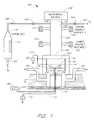
- FIG. 1is an electron cyclotron resonance chemical vapor deposition system according to an embodiment of the present invention.
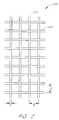
- FIG. 2is a top-view of a wire screens.
- An embodiment according to the inventionincludes a plasma enhanced or assisted chemical vapor deposition system, more particularly, an electron cyclotron resonance chemical vapor deposition (ECR CVD) system, which uniformly deposits a thin film of ferroelectric material having a controlled doping level.
- the materialcomprises zinc oxide (ZnO) with controlled amounts of metal doping, specifically lithium (Li) and/or magnesium (Mg), on a relatively large wafer.
- ZnOzinc oxide
- Mgmagnesium
- the production of the ferroelectric film on the relatively large wafercan result in a dramatic reduction to production costs as more devices can be formed at a time. For example, if a diameter of a given wafer doubles, the surface area of the wafer quadruples and can thereby accommodate approximately four times the number of devices.
- the ECR CVD systemcan control the doping of the Li and/or Mg such that the ferroelectric characteristics of the ZnO can be tailored to a desired characteristic. The tailoring of the ferroelectric characteristics further enhances the yield of processed
- FIG. 1illustrates an ECR CVD system 100 (not to scale) according to one embodiment of the invention.
- the ECR CVD systemis a plasma deposition technique, which also includes plasma assisted CVD and plasma enhanced CVD.
- the ECR CVD system 100includes a deposition chamber 102 , where a substrate 104 is processed.
- the chamber 102is configured to support a single wafer or substrate 104 , in accordance with state-of-the-art integrated circuit (IC) fabrication.
- the chamber 102can be configured to support a small number of substrates, e.g., less than 5 substrates, facing-the deposition sources.
- the components the ECR CVD system 100can be fabricated from a variety of materials including stainless steel.
- the deposition chamber 102can be formed within a cavity of fused quartz.
- the ECR CVD system 100includes an access door or port to provide access to the deposition chamber 102 for loading and unloading substrates.
- the substrate 104is placed on a substrate support, chuck or tray 106 , which rests on an insulator 108 that attaches to a stand 110 .
- the tray 106is preferably slightly larger in diameter than the substrate 104 .
- the tray 106and thereby the substrate 104 , can be connected to an external first power supply 112 through a first conductor 114 .
- the tray 106further provides attachment for guides 116 , which support a first grid 118 and a second grid 120 .
- the first and second grids 118 , 120are connected to a second power supply 122 through a second conductor 124 .
- the tray 106further includes a heat source 156 .
- the ECR CVD system 100further includes a plasma generator in the form of an electromagnetic excitation chamber 126 .
- Reactant source gasesare communicated to the excitation chamber 126 by reactant gas inlets 128 , which in the illustrated embodiment communicate with a vaporizer 130 .
- the electromagnetic excitation chamber 126also communicates with a microwave source 132 , an upper magnet assembly 134 , and a lower magnet assembly 136 .
- the vaporizer 130connects to at least one of the reactant gas inlets 128 via a first passage 138 and a mass flow controller or first valve 140 .
- a second passage 142 and a second valve 144couple another reactant gas inlet 128 , or a manifold leading to a common inlet, to an oxygen source.
- the microwave source 132couples to the electromagnetic excitation chamber 126 through a quartz window 146 .
- the upper and lower magnet assemblies 134 , 136can be attached to the electromagnetic excitation chamber 126 to create a magnetic field therein.
- the dashed line 148indicates the division between the deposition chamber 102 and the electromagnetic excitation chamber 126 .
- the electromagnetic excitation chamber 126is also known as a microwave plasma chamber.
- the deposition chamber 102is brought to a vacuum through vacuum pumps connected to evacuation outlets 150 .
- the systemis first evacuated to a base pressure below 2 ⁇ 10 ⁇ 6 Torr using a turbomolecular pump.
- Argon or other carrier gasis introduced into the vaporizer 130 through a vaporizer inlet 152 .
- the vaporizer 130contains a first source material 154 , such as Zn(C 5 H 7 O 2 ⁇ ) 2 or Zn(acac) 2 , where acac is acetyl acetonate.
- Zn(C 5 H 7 O 2 ⁇ ) 2is a precursor providing Zn.
- the vaporizer 130maintains the first source material 154 at approximately 105 degrees Celsius (C).
- the argon gas carrierintroduces the Zn precursor into the electromagnetic excitation chamber 126 through the reactant gas inlet 128 .
- the first valve 140controls the rate by which Zn is introduced into the electromagnetic excitation chamber 126 by controlling the rate at which argon flows through the vaporizer 130 .
- argonflows through the vaporizer 130 at approximately 100 cubic centimeters per minute.
- a second reactantcomprising a source of oxygen, such as diatomic oxygen (O 2 ) or ozone (O 3 ), is also introduced into the electromagnetic excitation chamber 126 via the reactant gas inlet 128 .
- the second valve 144controls the flow of oxygen source or precursor gas from the second passage 142 , which leads to the oxygen source.
- the oxygen precursorcomprises O 2 and the oxygen flow is approximately 2 cubic decimeters per minute. Varying the rate of gas flow and/or the gas flow ratio varies a rate of deposition of the dopants.
- the vacuum pumps and the first and the second valves 140 , 144maintain the pressure in the deposition chamber 102 at a relatively low vacuum, such as from 7 to 24 milliTorr (mTorr).
- the pressurecan vary widely, but higher pressures tend to weaken the electron cyclotron resonance effect and reduce the density of the plasma generated by the microwave source 132 .
- the pressure in the deposition chamber 102is maintained at 6 mTorr, although it can be monitored and maintained between about 7 mTorr to about 25 mTorr.
- the microwave source 132generates relatively high-powered microwaves, which are coupled to the electromagnetic excitation chamber 126 through the quartz window 146 .
- the microwave source 132can be remotely located from the electromagnetic excitation chamber 126 and coupled to the quartz window 146 with a waveguide.
- the microwave source 132is a magnetron that transmits approximately 300 to 400 Watts of microwave power to the electromagnetic excitation chamber 126 at a frequency of approximately 2.45 gigahertz (GHz).
- the energyis coupled to the reactant gases, breaking down Zn and oxygen precursors in the electromagnetic excitation chamber 126 to generate plasma ions and neutral radicals.
- the upper magnet assembly 134 and the lower magnet assembly 136induce a relatively powerful magnetic field within the electromagnetic excitation chamber 126 .
- the upper magnet assembly 134 and the lower magnet assembly 136can be fabricated from solenoids, where the windings of the solenoids wrap around the electromagnetic excitation chamber 126 as shown in FIG. 1.
- a magnetic flux density of approximately 875 Gauss produced in the middle of the electromagnetic excitation chamber 126suffices to allow an electron cyclotron resonance.
- the magnetic field produced by a solenoidcan vary with the current and the number of turns of wire in the solenoid.
- the current drive to an upper solenoid embodying the upper magnet assembly 134is approximately 20% greater than a current drive to a lower solenoid embodying the lower magnet assembly 136 such that the upper solenoid produces a greater magnetic field than the lower solenoid and thereby accelerates or propels ions within the plasma toward the deposition chamber 102 .
- the current drive to the upper and the lower solenoidscan conform to approximately 120 Amps and 100 Amps, respectively.
- the ferroelectric filmis deposited on the substrate 104 in the deposition chamber 102 .
- the substrate 104rests on a tray 106 , which is preferably heated by the heat source 156 .
- the tray 106can be fabricated from a material that is conductive to heat, such as a ceramic, such that the heat from the heat source 156 is relatively evenly distributed.
- a heat source 156passes a current through a resistive wire, such as NiChrome.
- a third power supply 158sources the current through wires 160 . The heat supplied can vary in accordance with the power applied to the resistive wire by the third power supply 158 .
- the tray 106can further include a temperature sensor, such as a thermocouple or temperature sensitive resistor, to monitor and/or control the temperature of the tray 106 .
- a temperature sensorsuch as a thermocouple or temperature sensitive resistor
- the heat source 156maintains the temperature of the tray 106 and the substrate 104 within a range of approximately 350 degrees C. to 650 degrees C.
- the substrate 104can be otherwise heated (e.g., inductively or radiantly).
- the rate at which ZnO is deposited on the substratecan be controlled by a position, a dimension, and a bias of the first and the second grids 118 , 120 .
- the first and the second grids 118 , 120also introduce a second source material that is sputtered on the substrate.
- the second source materialis a metal dopant, preferably Li and/or Mg, which combines with the dielectric ZnO to produce the ferroelectric film. Further details of a wire screen 200 that can form the first and the second grids 118 , 120 are described below in connection with FIG. 2 .
- the first and the second grids 118 , 120attach to the guides 116 , which hold the first and the second grids 118 , 120 above the substrate 104 .
- the guides 116are four insulating poles fabricated from an insulating polyimide polymer such as Vespel® from E. I. du Pont de Nemours and Company.
- the spacing between the first and the second grids 118 , 120 and the spacing between the first grid 118 and the substrate 104can be adjusted along the guides 116 to vary the rate of deposition.
- the spacing between the first and the second grids 118 , 120ranges from approximately 3 cm to 7 cm. More preferably, the spacing between the first and the second grids 118 , 120 ranges from approximately 4 cm to 6 cm.
- the spacing between the first and the second grids 118 , 120is approximately 5 cm.
- the spacing between the first grid 118 and the substrate 104ranges from approximately 2 cm to 5 cm. More preferably, the spacing between the first grid 118 and the substrate 104 ranges from approximately 2 cm to 3 cm. In one embodiment, the spacing between the first grid 118 and the substrate 104 is approximately 3 cm.
- the first and the second grids 118 , 120can be connected and biased through the second wire 124 and the second power supply.
- the voltage range for the biasing of the first and the second grids 118 , 120is approximately ⁇ 300 to ⁇ 350 Volts direct current (Vdc) relative to ground.
- the first and the second grids 118 , 120are not shorted together, but are connected to their own power supplies.
- the relatively large voltage range of ⁇ 300 to ⁇ 350 Vdcadvantageously reduces the coating of the first and the second grids 118 , 120 during the deposition process, which would otherwise reduce the incorporation of the Li and/or Mg in the ferroelectric film.
- the insulator 108isolates the tray 106 and the substrate 104 from ground potential.
- One embodiment of the insulator 108is fabricated from a quartz plate.
- the insulator 108permits biasing of the substrate 106 to a potential other than ground through the first conductor 114 and the first power supply 112 .
- the voltage range for the biasing of the substrateis approximately 0 to ⁇ 50 Vdc.
- the substrate 104 and the tray 106can simply be grounded without the insulator 108 when 0 Vdc is selected as the biasing of the substrate.
- FIG. 2illustrates a portion of the wire screen 200 according to one embodiment of the first and the second grids 118 , 120 .
- the first and the second grids 118 , 120are preferably circular in shape and larger in diameter than the diameter of the substrate 104 .
- the first and the second grids 118 , 120can be 35 cm in diameter.
- the portion of the wire screen 200 shownillustrates interwoven wires 210 , 220 .
- the diameter of the wire, represented by A in FIG. 2, and the spacing between wires, represented by B and C in FIG. 2,also varies the rate of deposition.
- the spacing between wirespreferably ranges from 3 mm to 5 mm, and more preferably from 4 mm to 5 mm.
- the wire diameterranges preferably from 0.5 mm to 1.2 mm, and more preferably from 1.0 mm to 1.2 mm. In one embodiment, for processing 300-mm wafers, the diameter of the wire, A, is in the range of approximately 0.5 to 1.0 mm and the spacing between the wires, B and C, is about 5 mm.
- the wiresare made from the desired dopant or dopants, specifically Li, Mg, or a combination of the two in the illustrated embodiment.
- the Li and/or Mg for the wirescan be produced by a relatively high purity process, such as a zonerefined process.
- Material from the wiresis deposited on the substrate 104 together with the ZnO as dopants to the ZnO to produce the ferroelectric film.
- the first and the second grids 118 , 120include both Li and Mg
- the ratio of the Li to Mg in the first and the second grids 118 , 120controls the ratio of the Li to Mg doping of the ferroelectric film.
- the ferroelectric properties of the ferroelectric filmcan thereby be conveniently tailored by selecting the desired ratio of Li to Mg in the first and the second grids, 118 , 120 .
- the ferroelectric filmexhibits ferroelectric properties.
- the ferroelectric filmis characterized by the general formula of Zn x (Li y Mg z )O, where x preferably ranges from approximately 0.70 to 0.99, y and z can independently range from approximately 0.00 to 0.30, and x, y, and z substantially sum to 1. More preferably, x ranges from approximately 0.80 to 0.95, y ranges from approximately 0.01 to 0.05, z ranges from approximately 0.04 to 0.15, and x, y, and z again substantially sum to 1. In one embodiment, x is about 0.9, y is about 0.02, and z is about 0.08.
- Embodiments of the present inventionadvantageously permit the fabrication of ferroelectric films on large substrates with high purity components and at relatively easily varied and controlled conditions.
- the control over the processallows for relatively high yields, which can lower production costs.
- a large substratefurther allows more devices to be fabricated at the same time, further reducing overall production costs.
Landscapes
- Chemical & Material Sciences (AREA)
- Engineering & Computer Science (AREA)
- Physics & Mathematics (AREA)
- Plasma & Fusion (AREA)
- Analytical Chemistry (AREA)
- Chemical Kinetics & Catalysis (AREA)
- General Chemical & Material Sciences (AREA)
- Materials Engineering (AREA)
- Mechanical Engineering (AREA)
- Metallurgy (AREA)
- Organic Chemistry (AREA)
- Inorganic Chemistry (AREA)
- Chemical Vapour Deposition (AREA)
Abstract
Description
Claims (38)
Priority Applications (3)
| Application Number | Priority Date | Filing Date | Title |
|---|---|---|---|
| US09/810,368US6454912B1 (en) | 2001-03-15 | 2001-03-15 | Method and apparatus for the fabrication of ferroelectric films |
| US10/217,212US6858120B2 (en) | 2001-03-15 | 2002-08-09 | Method and apparatus for the fabrication of ferroelectric films |
| US10/945,535US7041341B2 (en) | 2001-03-15 | 2004-09-20 | Process for the fabrication of oxide films |
Applications Claiming Priority (1)
| Application Number | Priority Date | Filing Date | Title |
|---|---|---|---|
| US09/810,368US6454912B1 (en) | 2001-03-15 | 2001-03-15 | Method and apparatus for the fabrication of ferroelectric films |
Related Child Applications (1)
| Application Number | Title | Priority Date | Filing Date |
|---|---|---|---|
| US10/217,212ContinuationUS6858120B2 (en) | 2001-03-15 | 2002-08-09 | Method and apparatus for the fabrication of ferroelectric films |
Publications (2)
| Publication Number | Publication Date |
|---|---|
| US20020130032A1 US20020130032A1 (en) | 2002-09-19 |
| US6454912B1true US6454912B1 (en) | 2002-09-24 |
Family
ID=25203699
Family Applications (3)
| Application Number | Title | Priority Date | Filing Date |
|---|---|---|---|
| US09/810,368Expired - LifetimeUS6454912B1 (en) | 2001-03-15 | 2001-03-15 | Method and apparatus for the fabrication of ferroelectric films |
| US10/217,212Expired - Fee RelatedUS6858120B2 (en) | 2001-03-15 | 2002-08-09 | Method and apparatus for the fabrication of ferroelectric films |
| US10/945,535Expired - Fee RelatedUS7041341B2 (en) | 2001-03-15 | 2004-09-20 | Process for the fabrication of oxide films |
Family Applications After (2)
| Application Number | Title | Priority Date | Filing Date |
|---|---|---|---|
| US10/217,212Expired - Fee RelatedUS6858120B2 (en) | 2001-03-15 | 2002-08-09 | Method and apparatus for the fabrication of ferroelectric films |
| US10/945,535Expired - Fee RelatedUS7041341B2 (en) | 2001-03-15 | 2004-09-20 | Process for the fabrication of oxide films |
Country Status (1)
| Country | Link |
|---|---|
| US (3) | US6454912B1 (en) |
Cited By (47)
| Publication number | Priority date | Publication date | Assignee | Title |
|---|---|---|---|---|
| US20020185374A1 (en)* | 2001-03-15 | 2002-12-12 | Micron Technology, Inc. | Method and apparatus for the fabrication of ferroelectric films |
| US20040089233A1 (en)* | 2002-04-11 | 2004-05-13 | Carpenter Craig M. | Deposition methods utilizing microwave excitation |
| US20050186731A1 (en)* | 2004-02-19 | 2005-08-25 | Derderian Garo J. | Atomic layer deposition method of forming an oxide comprising layer on a substrate |
| US20060134345A1 (en)* | 2004-12-20 | 2006-06-22 | Micron Technology, Inc. | Systems and methods for depositing material onto microfeature workpieces |
| US7081421B2 (en) | 2004-08-26 | 2006-07-25 | Micron Technology, Inc. | Lanthanide oxide dielectric layer |
| US7160577B2 (en) | 2002-05-02 | 2007-01-09 | Micron Technology, Inc. | Methods for atomic-layer deposition of aluminum oxides in integrated circuits |
| US7205218B2 (en) | 2002-06-05 | 2007-04-17 | Micron Technology, Inc. | Method including forming gate dielectrics having multiple lanthanide oxide layers |
| US20070110644A1 (en)* | 2003-12-03 | 2007-05-17 | Yasuhiko Kasama | System for manufacturing a fullerene derivative and method for manufacturing |
| US7235854B2 (en) | 2002-08-15 | 2007-06-26 | Micron Technology, Inc. | Lanthanide doped TiOx dielectric films |
| US7259434B2 (en) | 2001-08-30 | 2007-08-21 | Micron Technology, Inc. | Highly reliable amorphous high-k gate oxide ZrO2 |
| US7326980B2 (en) | 2002-08-28 | 2008-02-05 | Micron Technology, Inc. | Devices with HfSiON dielectric films which are Hf-O rich |
| US7374964B2 (en) | 2005-02-10 | 2008-05-20 | Micron Technology, Inc. | Atomic layer deposition of CeO2/Al2O3 films as gate dielectrics |
| US7388246B2 (en) | 2002-08-29 | 2008-06-17 | Micron Technology, Inc. | Lanthanide doped TiOx dielectric films |
| US7402876B2 (en) | 2002-12-04 | 2008-07-22 | Micron Technology, Inc. | Zr— Sn—Ti—O films |
| US7405454B2 (en) | 2003-03-04 | 2008-07-29 | Micron Technology, Inc. | Electronic apparatus with deposited dielectric layers |
| US7410668B2 (en) | 2001-03-01 | 2008-08-12 | Micron Technology, Inc. | Methods, systems, and apparatus for uniform chemical-vapor depositions |
| US7410910B2 (en) | 2005-08-31 | 2008-08-12 | Micron Technology, Inc. | Lanthanum aluminum oxynitride dielectric films |
| DE102007025151A1 (en)* | 2007-05-29 | 2008-09-04 | Innovent E.V. | Coating method comprises producing plasma jet from process gas and introducing precursor material into it, coating being deposited from jet on to substrate or existing coating on it and substrate being heated |
| US7439194B2 (en) | 2002-08-15 | 2008-10-21 | Micron Technology, Inc. | Lanthanide doped TiOx dielectric films by plasma oxidation |
| DE102007025152A1 (en)* | 2007-05-29 | 2008-12-04 | Innovent E.V. | Method for coating a substrate |
| US7476925B2 (en) | 2001-08-30 | 2009-01-13 | Micron Technology, Inc. | Atomic layer deposition of metal oxide and/or low asymmetrical tunnel barrier interploy insulators |
| US7494939B2 (en) | 2004-08-31 | 2009-02-24 | Micron Technology, Inc. | Methods for forming a lanthanum-metal oxide dielectric layer |
| US20090075687A1 (en)* | 2005-05-15 | 2009-03-19 | Sony Computer Entertainment Inc. | Center Device |
| US7545674B2 (en) | 2001-08-30 | 2009-06-09 | Micron Technology, Inc. | Flash memory with low tunnel barrier interpoly insulators |
| US7554161B2 (en) | 2002-06-05 | 2009-06-30 | Micron Technology, Inc. | HfAlO3 films for gate dielectrics |
| US7560395B2 (en) | 2005-01-05 | 2009-07-14 | Micron Technology, Inc. | Atomic layer deposited hafnium tantalum oxide dielectrics |
| US7560793B2 (en) | 2002-05-02 | 2009-07-14 | Micron Technology, Inc. | Atomic layer deposition and conversion |
| US7572695B2 (en) | 2005-05-27 | 2009-08-11 | Micron Technology, Inc. | Hafnium titanium oxide films |
| US7581511B2 (en) | 2003-10-10 | 2009-09-01 | Micron Technology, Inc. | Apparatus and methods for manufacturing microfeatures on workpieces using plasma vapor processes |
| US7588804B2 (en) | 2002-08-15 | 2009-09-15 | Micron Technology, Inc. | Reactors with isolated gas connectors and methods for depositing materials onto micro-device workpieces |
| US7601649B2 (en) | 2004-08-02 | 2009-10-13 | Micron Technology, Inc. | Zirconium-doped tantalum oxide films |
| US7611959B2 (en) | 2002-12-04 | 2009-11-03 | Micron Technology, Inc. | Zr-Sn-Ti-O films |
| US7625794B2 (en) | 2003-03-31 | 2009-12-01 | Micron Technology, Inc. | Methods of forming zirconium aluminum oxide |
| US7662729B2 (en) | 2005-04-28 | 2010-02-16 | Micron Technology, Inc. | Atomic layer deposition of a ruthenium layer to a lanthanide oxide dielectric layer |
| US7687848B2 (en) | 2002-07-08 | 2010-03-30 | Micron Technology, Inc. | Memory utilizing oxide-conductor nanolaminates |
| US7687409B2 (en) | 2005-03-29 | 2010-03-30 | Micron Technology, Inc. | Atomic layer deposited titanium silicon oxide films |
| US7699932B2 (en) | 2004-06-02 | 2010-04-20 | Micron Technology, Inc. | Reactors, systems and methods for depositing thin films onto microfeature workpieces |
| US7709402B2 (en) | 2006-02-16 | 2010-05-04 | Micron Technology, Inc. | Conductive layers for hafnium silicon oxynitride films |
| US7728626B2 (en) | 2002-07-08 | 2010-06-01 | Micron Technology, Inc. | Memory utilizing oxide nanolaminates |
| US20100276748A1 (en)* | 2007-06-28 | 2010-11-04 | Ahn Kie Y | Method of forming lutetium and lanthanum dielectric structures |
| US7869242B2 (en) | 1999-07-30 | 2011-01-11 | Micron Technology, Inc. | Transmission lines for CMOS integrated circuits |
| US8071476B2 (en) | 2005-08-31 | 2011-12-06 | Micron Technology, Inc. | Cobalt titanium oxide dielectric films |
| US8133554B2 (en) | 2004-05-06 | 2012-03-13 | Micron Technology, Inc. | Methods for depositing material onto microfeature workpieces in reaction chambers and systems for depositing materials onto microfeature workpieces |
| US8501563B2 (en) | 2005-07-20 | 2013-08-06 | Micron Technology, Inc. | Devices with nanocrystals and methods of formation |
| WO2014037646A1 (en)* | 2012-09-07 | 2014-03-13 | Commissariat A L'energie Atomique Et Aux Energies Alternatives | Method for producing a lithium-based electrolyte for a solid microbattery |
| US20150225845A1 (en)* | 2014-02-12 | 2015-08-13 | Electronics And Telecommunications Research Institute | Method for forming metal oxide thin film and device for printing metal oxide thin film |
| US20210262117A1 (en)* | 2020-02-24 | 2021-08-26 | J2 Materials, Llc | Plasma shaping for diamond growth |
Families Citing this family (18)
| Publication number | Priority date | Publication date | Assignee | Title |
|---|---|---|---|---|
| US7192824B2 (en)* | 2003-06-24 | 2007-03-20 | Micron Technology, Inc. | Lanthanide oxide / hafnium oxide dielectric layers |
| DE602004017518D1 (en)* | 2004-04-06 | 2008-12-11 | Lg Electronics Inc | METAL PRODUCT COATED WITH ULTRAHYDROPHILIC AND ANTIBACTERIAL THIN FILM AND METHOD OF MANUFACTURING THEREOF |
| US20060073276A1 (en)* | 2004-10-04 | 2006-04-06 | Eric Antonissen | Multi-zone atomic layer deposition apparatus and method |
| US20060125030A1 (en)* | 2004-12-13 | 2006-06-15 | Micron Technology, Inc. | Hybrid ALD-CVD of PrxOy/ZrO2 films as gate dielectrics |
| US7620476B2 (en)* | 2005-02-18 | 2009-11-17 | Irobot Corporation | Autonomous surface cleaning robot for dry cleaning |
| US8110469B2 (en)* | 2005-08-30 | 2012-02-07 | Micron Technology, Inc. | Graded dielectric layers |
| US7442413B2 (en)* | 2005-11-18 | 2008-10-28 | Daystar Technologies, Inc. | Methods and apparatus for treating a work piece with a vaporous element |
| EP1918965A1 (en)* | 2006-11-02 | 2008-05-07 | Dow Corning Corporation | Method and apparatus for forming a film by deposition from a plasma |
| US7972469B2 (en)* | 2007-04-22 | 2011-07-05 | Applied Materials, Inc. | Plasma processing apparatus |
| US20080260966A1 (en)* | 2007-04-22 | 2008-10-23 | Applied Materials, Inc. | Plasma processing method |
| WO2010027841A2 (en)* | 2008-08-27 | 2010-03-11 | Ovshinsky Innovation | High speed deposition of materials having low defect density |
| US7875948B2 (en)* | 2008-10-21 | 2011-01-25 | Jaroslav Hynecek | Backside illuminated image sensor |
| JP2012167317A (en)* | 2011-02-14 | 2012-09-06 | Mitsui Eng & Shipbuild Co Ltd | Atomic layer deposition apparatus |
| CN104024469B (en)* | 2011-09-02 | 2017-05-03 | 第一太阳能有限公司 | Feeder system and method for a vapor transport deposition system |
| KR20140077020A (en)* | 2012-12-13 | 2014-06-23 | 삼성디스플레이 주식회사 | A sputtering apparatus |
| CN103014655A (en)* | 2012-12-27 | 2013-04-03 | 沈阳工程学院 | Preparation method of Ga/Al-codoped ZnO film by ECR-PEMOCVD (electron cyclotron resonance-plasma-enhanced metal-organic chemical vapor deposition) low-temperature deposition |
| US20150240349A1 (en)* | 2014-02-27 | 2015-08-27 | Avago Technologies General Ip (Singapore) Pte. Ltd. | Magnetron sputtering device and method of fabricating thin film using magnetron sputtering device |
| CN109837520A (en)* | 2018-12-20 | 2019-06-04 | 兰州空间技术物理研究所 | The shaft and installation method of the rotational workpieces of voltage and temperature measurement signal coaxial conductive |
Citations (1)
| Publication number | Priority date | Publication date | Assignee | Title |
|---|---|---|---|---|
| US5965192A (en)* | 1996-09-03 | 1999-10-12 | Advanced Vision Technologies, Inc. | Processes for oxide based phosphors |
Family Cites Families (4)
| Publication number | Priority date | Publication date | Assignee | Title |
|---|---|---|---|---|
| US6083363A (en)* | 1997-07-02 | 2000-07-04 | Tokyo Electron Limited | Apparatus and method for uniform, low-damage anisotropic plasma processing |
| JP2000017457A (en)* | 1998-07-03 | 2000-01-18 | Shincron:Kk | Thin film forming apparatus and thin film forming method |
| US6498362B1 (en) | 1999-08-26 | 2002-12-24 | Micron Technology, Inc. | Weak ferroelectric transistor |
| US6454912B1 (en)* | 2001-03-15 | 2002-09-24 | Micron Technology, Inc. | Method and apparatus for the fabrication of ferroelectric films |
- 2001
- 2001-03-15USUS09/810,368patent/US6454912B1/ennot_activeExpired - Lifetime
- 2002
- 2002-08-09USUS10/217,212patent/US6858120B2/ennot_activeExpired - Fee Related
- 2004
- 2004-09-20USUS10/945,535patent/US7041341B2/ennot_activeExpired - Fee Related
Patent Citations (1)
| Publication number | Priority date | Publication date | Assignee | Title |
|---|---|---|---|---|
| US5965192A (en)* | 1996-09-03 | 1999-10-12 | Advanced Vision Technologies, Inc. | Processes for oxide based phosphors |
Non-Patent Citations (8)
| Title |
|---|
| Akira Onodera, et al., Ferroelectric Properties in Piezoelectric Semiconductor Zn1-xMxO (M=Li, Mg), Japanese Journal of Applied Physics, vol. 36, Part 1, No. 9B (1997), pp. 6008 to 6011. |
| Baosheng Sang, et al., Highly Stable ZnO Thin Films by Atomic Layer Deposition, Japanese Journal of Applied Physics, vol. 37, Part 2, No. 10A (Oct. 1, 1998), pp. L1125 to L1128. |
| Junichi Nishino, et al., Preparation of Zinc Oxide Films by Low-Pressure Chemical Vapor Deposition Method, Materials Research Society Symposium Proceedings, vol. 363 (1995), pp. 219 to 224. |
| Rusli, et al., Influence of Process Pressure on the Growth of Hydrocarbon Films Under Direct DC Bias in an Electron Cyclotron Resonance Plasma, Journal of Applied Physics, vol. 84, No. 9 (Nov. 1, 1998), pp. 5277 to 5282. |
| Rusli, et al., Investigation of Tungsten Incorporated Amorphous Carbon Film, Thin Solid Films, vol. 355-356 (1999), pp. 174 to 178. |
| S.F. Yoon et al., Influence of Substrate Temperature and Microwave Power on the Properties of a-C:H Films Prepared Using the ECR-CVD Method, Diamond and Related Materials, vol. 6(1997), pp. 1683-1688. |
| S.F. Yoon, et al., Deposition of Diamond-Like Carbon Films Using the Screen Grid Method in Electron Cyclotron Resonance Chemical Vapor Deposition, Journal of Vacuum Science and Technology A 17(1) (Jan/Feb 1999), pp. 121 to 124. |
| U.S. patent application Ser. No. 09/383,726. |
Cited By (96)
| Publication number | Priority date | Publication date | Assignee | Title |
|---|---|---|---|---|
| US7869242B2 (en) | 1999-07-30 | 2011-01-11 | Micron Technology, Inc. | Transmission lines for CMOS integrated circuits |
| US7410668B2 (en) | 2001-03-01 | 2008-08-12 | Micron Technology, Inc. | Methods, systems, and apparatus for uniform chemical-vapor depositions |
| US7041341B2 (en) | 2001-03-15 | 2006-05-09 | Micron Technology, Inc. | Process for the fabrication of oxide films |
| US6858120B2 (en)* | 2001-03-15 | 2005-02-22 | Micron Technology, Inc. | Method and apparatus for the fabrication of ferroelectric films |
| US20050118354A1 (en)* | 2001-03-15 | 2005-06-02 | Ahn Kie Y. | Process for the fabrication of oxide films |
| US20020185374A1 (en)* | 2001-03-15 | 2002-12-12 | Micron Technology, Inc. | Method and apparatus for the fabrication of ferroelectric films |
| US8652957B2 (en) | 2001-08-30 | 2014-02-18 | Micron Technology, Inc. | High-K gate dielectric oxide |
| US8026161B2 (en) | 2001-08-30 | 2011-09-27 | Micron Technology, Inc. | Highly reliable amorphous high-K gate oxide ZrO2 |
| US7476925B2 (en) | 2001-08-30 | 2009-01-13 | Micron Technology, Inc. | Atomic layer deposition of metal oxide and/or low asymmetrical tunnel barrier interploy insulators |
| US7545674B2 (en) | 2001-08-30 | 2009-06-09 | Micron Technology, Inc. | Flash memory with low tunnel barrier interpoly insulators |
| US7259434B2 (en) | 2001-08-30 | 2007-08-21 | Micron Technology, Inc. | Highly reliable amorphous high-k gate oxide ZrO2 |
| US7422986B2 (en)* | 2002-04-11 | 2008-09-09 | Micron Technology, Inc. | Deposition methods utilizing microwave excitation |
| US20040089233A1 (en)* | 2002-04-11 | 2004-05-13 | Carpenter Craig M. | Deposition methods utilizing microwave excitation |
| US7105208B2 (en)* | 2002-04-11 | 2006-09-12 | Micron Technology, Inc. | Methods and processes utilizing microwave excitation |
| US20070036895A1 (en)* | 2002-04-11 | 2007-02-15 | Carpenter Craig M | Deposition methods utilizing microwave excitation |
| US7560793B2 (en) | 2002-05-02 | 2009-07-14 | Micron Technology, Inc. | Atomic layer deposition and conversion |
| US7160577B2 (en) | 2002-05-02 | 2007-01-09 | Micron Technology, Inc. | Methods for atomic-layer deposition of aluminum oxides in integrated circuits |
| US7670646B2 (en) | 2002-05-02 | 2010-03-02 | Micron Technology, Inc. | Methods for atomic-layer deposition |
| US7589029B2 (en) | 2002-05-02 | 2009-09-15 | Micron Technology, Inc. | Atomic layer deposition and conversion |
| US7554161B2 (en) | 2002-06-05 | 2009-06-30 | Micron Technology, Inc. | HfAlO3 films for gate dielectrics |
| US7205218B2 (en) | 2002-06-05 | 2007-04-17 | Micron Technology, Inc. | Method including forming gate dielectrics having multiple lanthanide oxide layers |
| US8093638B2 (en) | 2002-06-05 | 2012-01-10 | Micron Technology, Inc. | Systems with a gate dielectric having multiple lanthanide oxide layers |
| US7687848B2 (en) | 2002-07-08 | 2010-03-30 | Micron Technology, Inc. | Memory utilizing oxide-conductor nanolaminates |
| US7728626B2 (en) | 2002-07-08 | 2010-06-01 | Micron Technology, Inc. | Memory utilizing oxide nanolaminates |
| US8228725B2 (en) | 2002-07-08 | 2012-07-24 | Micron Technology, Inc. | Memory utilizing oxide nanolaminates |
| US7588804B2 (en) | 2002-08-15 | 2009-09-15 | Micron Technology, Inc. | Reactors with isolated gas connectors and methods for depositing materials onto micro-device workpieces |
| US7439194B2 (en) | 2002-08-15 | 2008-10-21 | Micron Technology, Inc. | Lanthanide doped TiOx dielectric films by plasma oxidation |
| US7235854B2 (en) | 2002-08-15 | 2007-06-26 | Micron Technology, Inc. | Lanthanide doped TiOx dielectric films |
| US7326980B2 (en) | 2002-08-28 | 2008-02-05 | Micron Technology, Inc. | Devices with HfSiON dielectric films which are Hf-O rich |
| US7388246B2 (en) | 2002-08-29 | 2008-06-17 | Micron Technology, Inc. | Lanthanide doped TiOx dielectric films |
| US7402876B2 (en) | 2002-12-04 | 2008-07-22 | Micron Technology, Inc. | Zr— Sn—Ti—O films |
| US7611959B2 (en) | 2002-12-04 | 2009-11-03 | Micron Technology, Inc. | Zr-Sn-Ti-O films |
| US7410917B2 (en) | 2002-12-04 | 2008-08-12 | Micron Technology, Inc. | Atomic layer deposited Zr-Sn-Ti-O films using TiI4 |
| US8445952B2 (en) | 2002-12-04 | 2013-05-21 | Micron Technology, Inc. | Zr-Sn-Ti-O films |
| US7405454B2 (en) | 2003-03-04 | 2008-07-29 | Micron Technology, Inc. | Electronic apparatus with deposited dielectric layers |
| US7625794B2 (en) | 2003-03-31 | 2009-12-01 | Micron Technology, Inc. | Methods of forming zirconium aluminum oxide |
| US7581511B2 (en) | 2003-10-10 | 2009-09-01 | Micron Technology, Inc. | Apparatus and methods for manufacturing microfeatures on workpieces using plasma vapor processes |
| US20070110644A1 (en)* | 2003-12-03 | 2007-05-17 | Yasuhiko Kasama | System for manufacturing a fullerene derivative and method for manufacturing |
| US20060029737A1 (en)* | 2004-02-19 | 2006-02-09 | Micron Technology, Inc. | Atomic layer deposition method of forming an oxide comprising layer on a substrate |
| US7067438B2 (en) | 2004-02-19 | 2006-06-27 | Micron Technology, Inc. | Atomic layer deposition method of forming an oxide comprising layer on a substrate |
| US7119034B2 (en) | 2004-02-19 | 2006-10-10 | Micron Technology, Inc. | Atomic layer deposition method of forming an oxide comprising layer on a substrate |
| US20050186731A1 (en)* | 2004-02-19 | 2005-08-25 | Derderian Garo J. | Atomic layer deposition method of forming an oxide comprising layer on a substrate |
| US7329615B2 (en) | 2004-02-19 | 2008-02-12 | Micron Technology, Inc. | Atomic layer deposition method of forming an oxide comprising layer on a substrate |
| US20060003102A1 (en)* | 2004-02-19 | 2006-01-05 | Derderian Garo J | Atomic layer deposition method of forming an oxide comprising layer on a substrate |
| US9023436B2 (en) | 2004-05-06 | 2015-05-05 | Micron Technology, Inc. | Methods for depositing material onto microfeature workpieces in reaction chambers and systems for depositing materials onto microfeature workpieces |
| US8133554B2 (en) | 2004-05-06 | 2012-03-13 | Micron Technology, Inc. | Methods for depositing material onto microfeature workpieces in reaction chambers and systems for depositing materials onto microfeature workpieces |
| US7699932B2 (en) | 2004-06-02 | 2010-04-20 | Micron Technology, Inc. | Reactors, systems and methods for depositing thin films onto microfeature workpieces |
| US8288809B2 (en) | 2004-08-02 | 2012-10-16 | Micron Technology, Inc. | Zirconium-doped tantalum oxide films |
| US7601649B2 (en) | 2004-08-02 | 2009-10-13 | Micron Technology, Inc. | Zirconium-doped tantalum oxide films |
| US7727905B2 (en) | 2004-08-02 | 2010-06-01 | Micron Technology, Inc. | Zirconium-doped tantalum oxide films |
| US8765616B2 (en) | 2004-08-02 | 2014-07-01 | Micron Technology, Inc. | Zirconium-doped tantalum oxide films |
| US7776762B2 (en) | 2004-08-02 | 2010-08-17 | Micron Technology, Inc. | Zirconium-doped tantalum oxide films |
| US7719065B2 (en) | 2004-08-26 | 2010-05-18 | Micron Technology, Inc. | Ruthenium layer for a dielectric layer containing a lanthanide oxide |
| US8558325B2 (en) | 2004-08-26 | 2013-10-15 | Micron Technology, Inc. | Ruthenium for a dielectric containing a lanthanide |
| US8907486B2 (en) | 2004-08-26 | 2014-12-09 | Micron Technology, Inc. | Ruthenium for a dielectric containing a lanthanide |
| US7081421B2 (en) | 2004-08-26 | 2006-07-25 | Micron Technology, Inc. | Lanthanide oxide dielectric layer |
| US7867919B2 (en) | 2004-08-31 | 2011-01-11 | Micron Technology, Inc. | Method of fabricating an apparatus having a lanthanum-metal oxide dielectric layer |
| US8237216B2 (en) | 2004-08-31 | 2012-08-07 | Micron Technology, Inc. | Apparatus having a lanthanum-metal oxide semiconductor device |
| US7494939B2 (en) | 2004-08-31 | 2009-02-24 | Micron Technology, Inc. | Methods for forming a lanthanum-metal oxide dielectric layer |
| US20060134345A1 (en)* | 2004-12-20 | 2006-06-22 | Micron Technology, Inc. | Systems and methods for depositing material onto microfeature workpieces |
| US8524618B2 (en) | 2005-01-05 | 2013-09-03 | Micron Technology, Inc. | Hafnium tantalum oxide dielectrics |
| US7560395B2 (en) | 2005-01-05 | 2009-07-14 | Micron Technology, Inc. | Atomic layer deposited hafnium tantalum oxide dielectrics |
| US7602030B2 (en) | 2005-01-05 | 2009-10-13 | Micron Technology, Inc. | Hafnium tantalum oxide dielectrics |
| US8278225B2 (en) | 2005-01-05 | 2012-10-02 | Micron Technology, Inc. | Hafnium tantalum oxide dielectrics |
| US7374964B2 (en) | 2005-02-10 | 2008-05-20 | Micron Technology, Inc. | Atomic layer deposition of CeO2/Al2O3 films as gate dielectrics |
| US7518246B2 (en) | 2005-02-10 | 2009-04-14 | Micron Technology, Inc. | Atomic layer deposition of CeO2/Al2O3 films as gate dielectrics |
| US7754618B2 (en) | 2005-02-10 | 2010-07-13 | Micron Technology, Inc. | Method of forming an apparatus having a dielectric containing cerium oxide and aluminum oxide |
| US8399365B2 (en) | 2005-03-29 | 2013-03-19 | Micron Technology, Inc. | Methods of forming titanium silicon oxide |
| US8076249B2 (en) | 2005-03-29 | 2011-12-13 | Micron Technology, Inc. | Structures containing titanium silicon oxide |
| US7687409B2 (en) | 2005-03-29 | 2010-03-30 | Micron Technology, Inc. | Atomic layer deposited titanium silicon oxide films |
| US7662729B2 (en) | 2005-04-28 | 2010-02-16 | Micron Technology, Inc. | Atomic layer deposition of a ruthenium layer to a lanthanide oxide dielectric layer |
| US20090075687A1 (en)* | 2005-05-15 | 2009-03-19 | Sony Computer Entertainment Inc. | Center Device |
| US7700989B2 (en) | 2005-05-27 | 2010-04-20 | Micron Technology, Inc. | Hafnium titanium oxide films |
| US7572695B2 (en) | 2005-05-27 | 2009-08-11 | Micron Technology, Inc. | Hafnium titanium oxide films |
| US8921914B2 (en) | 2005-07-20 | 2014-12-30 | Micron Technology, Inc. | Devices with nanocrystals and methods of formation |
| US8501563B2 (en) | 2005-07-20 | 2013-08-06 | Micron Technology, Inc. | Devices with nanocrystals and methods of formation |
| US7410910B2 (en) | 2005-08-31 | 2008-08-12 | Micron Technology, Inc. | Lanthanum aluminum oxynitride dielectric films |
| US8895442B2 (en) | 2005-08-31 | 2014-11-25 | Micron Technology, Inc. | Cobalt titanium oxide dielectric films |
| US7531869B2 (en) | 2005-08-31 | 2009-05-12 | Micron Technology, Inc. | Lanthanum aluminum oxynitride dielectric films |
| US8455959B2 (en) | 2005-08-31 | 2013-06-04 | Micron Technology, Inc. | Apparatus containing cobalt titanium oxide |
| US8071476B2 (en) | 2005-08-31 | 2011-12-06 | Micron Technology, Inc. | Cobalt titanium oxide dielectric films |
| US8067794B2 (en) | 2006-02-16 | 2011-11-29 | Micron Technology, Inc. | Conductive layers for hafnium silicon oxynitride films |
| US7709402B2 (en) | 2006-02-16 | 2010-05-04 | Micron Technology, Inc. | Conductive layers for hafnium silicon oxynitride films |
| US8785312B2 (en) | 2006-02-16 | 2014-07-22 | Micron Technology, Inc. | Conductive layers for hafnium silicon oxynitride |
| DE102007025152A1 (en)* | 2007-05-29 | 2008-12-04 | Innovent E.V. | Method for coating a substrate |
| DE102007025151A1 (en)* | 2007-05-29 | 2008-09-04 | Innovent E.V. | Coating method comprises producing plasma jet from process gas and introducing precursor material into it, coating being deposited from jet on to substrate or existing coating on it and substrate being heated |
| DE102007025152B4 (en)* | 2007-05-29 | 2012-02-09 | Innovent E.V. | Method for coating a substrate |
| US20100143602A1 (en)* | 2007-05-29 | 2010-06-10 | Andreas Heft | Method for coating a substrate |
| US8847334B2 (en) | 2007-06-28 | 2014-09-30 | Micron Technology, Inc. | Method of forming lutetium and lanthanum dielectric structures |
| US8071443B2 (en) | 2007-06-28 | 2011-12-06 | Micron Technology, Inc. | Method of forming lutetium and lanthanum dielectric structures |
| US20100276748A1 (en)* | 2007-06-28 | 2010-11-04 | Ahn Kie Y | Method of forming lutetium and lanthanum dielectric structures |
| FR2995454A1 (en)* | 2012-09-07 | 2014-03-14 | Commissariat Energie Atomique | PROCESS FOR PRODUCING LITHIUM ELECTROLYTE FOR SOLID MICRO-BATTERY |
| WO2014037646A1 (en)* | 2012-09-07 | 2014-03-13 | Commissariat A L'energie Atomique Et Aux Energies Alternatives | Method for producing a lithium-based electrolyte for a solid microbattery |
| US9722278B2 (en) | 2012-09-07 | 2017-08-01 | Commissariat A L'energie Atomique Et Aux Energies Alternatives | Method for producing a lithium-based electrolyte for a solid microbattery |
| US20150225845A1 (en)* | 2014-02-12 | 2015-08-13 | Electronics And Telecommunications Research Institute | Method for forming metal oxide thin film and device for printing metal oxide thin film |
| US20210262117A1 (en)* | 2020-02-24 | 2021-08-26 | J2 Materials, Llc | Plasma shaping for diamond growth |
Also Published As
| Publication number | Publication date |
|---|---|
| US20020130032A1 (en) | 2002-09-19 |
| US6858120B2 (en) | 2005-02-22 |
| US20050118354A1 (en) | 2005-06-02 |
| US20020185374A1 (en) | 2002-12-12 |
| US7041341B2 (en) | 2006-05-09 |
Similar Documents
| Publication | Publication Date | Title |
|---|---|---|
| US6454912B1 (en) | Method and apparatus for the fabrication of ferroelectric films | |
| US4844775A (en) | Ion etching and chemical vapour deposition | |
| US6300227B1 (en) | Enhanced plasma mode and system for plasma immersion ion implantation | |
| US5279669A (en) | Plasma reactor for processing substrates comprising means for inducing electron cyclotron resonance (ECR) and ion cyclotron resonance (ICR) conditions | |
| US6213050B1 (en) | Enhanced plasma mode and computer system for plasma immersion ion implantation | |
| KR100445018B1 (en) | Method and Apparatus for Metallizing High Aspect Ratio Silicon Semiconductor Device Contacts | |
| KR100943695B1 (en) | Atomic Layer Deposition Reactor | |
| JP5698652B2 (en) | Coaxial microwave assisted deposition and etching system | |
| US5178739A (en) | Apparatus for depositing material into high aspect ratio holes | |
| KR101762528B1 (en) | Solid state introduction of dopants for plasma doping | |
| US6417111B2 (en) | Plasma processing apparatus | |
| US5651825A (en) | Plasma generating apparatus and plasma processing apparatus | |
| US20100323113A1 (en) | Method to Synthesize Graphene | |
| WO1993018201A1 (en) | Plasma implantation process and equipment | |
| JPH07268622A (en) | Microwave plasma sticking source | |
| EP0776991B1 (en) | Plasma annealing of thin films | |
| US9011634B2 (en) | Plasma processing apparatus and plasma processing method | |
| JP2004047695A (en) | Plasma doping method and apparatus | |
| JP2000068227A (en) | Method for processing surface and device thereof | |
| CN106103787A (en) | Process gas segmentation for static reaction sputtering | |
| JP2002531914A (en) | Enhanced plasma mode, method and system for plasma immersion ion implantation | |
| JP4303662B2 (en) | Plasma processing method | |
| Felmetsger et al. | Design, operation mode, and stress control capability of S-Gun magnetron for ac reactive sputtering | |
| KR102340365B1 (en) | An antenna structure for a high density linear ICP source | |
| JP3220528B2 (en) | Vacuum processing equipment |
Legal Events
| Date | Code | Title | Description |
|---|---|---|---|
| AS | Assignment | Owner name:MICRON TECHNOLOGY, INC., IDAHO Free format text:ASSIGNMENT OF ASSIGNORS INTEREST;ASSIGNORS:AHN, KIE Y.;FORBES, LEONARD;REEL/FRAME:011631/0685;SIGNING DATES FROM 20010307 TO 20010308 | |
| STCF | Information on status: patent grant | Free format text:PATENTED CASE | |
| FEPP | Fee payment procedure | Free format text:PAYOR NUMBER ASSIGNED (ORIGINAL EVENT CODE: ASPN); ENTITY STATUS OF PATENT OWNER: LARGE ENTITY | |
| FEPP | Fee payment procedure | Free format text:PAYOR NUMBER ASSIGNED (ORIGINAL EVENT CODE: ASPN); ENTITY STATUS OF PATENT OWNER: LARGE ENTITY Free format text:PAYER NUMBER DE-ASSIGNED (ORIGINAL EVENT CODE: RMPN); ENTITY STATUS OF PATENT OWNER: LARGE ENTITY | |
| FPAY | Fee payment | Year of fee payment:4 | |
| FEPP | Fee payment procedure | Free format text:PAYER NUMBER DE-ASSIGNED (ORIGINAL EVENT CODE: RMPN); ENTITY STATUS OF PATENT OWNER: LARGE ENTITY Free format text:PAYOR NUMBER ASSIGNED (ORIGINAL EVENT CODE: ASPN); ENTITY STATUS OF PATENT OWNER: LARGE ENTITY | |
| AS | Assignment | Owner name:MOSAID TECHNOLOGIES INCORPORATED, CANADA Free format text:ASSIGNMENT OF ASSIGNORS INTEREST;ASSIGNOR:MICRON TECHNOLOGY, INC.;REEL/FRAME:023574/0723 Effective date:20090609 | |
| FPAY | Fee payment | Year of fee payment:8 | |
| AS | Assignment | Owner name:ROYAL BANK OF CANADA, CANADA Free format text:U.S. INTELLECTUAL PROPERTY SECURITY AGREEMENT (FOR NON-U.S. GRANTORS) - SHORT FORM;ASSIGNORS:658276 N.B. LTD.;658868 N.B. INC.;MOSAID TECHNOLOGIES INCORPORATED;REEL/FRAME:027512/0196 Effective date:20111223 | |
| AS | Assignment | Owner name:CONVERSANT INTELLECTUAL PROPERTY MANAGEMENT INC., Free format text:CHANGE OF NAME;ASSIGNOR:MOSAID TECHNOLOGIES INCORPORATED;REEL/FRAME:032439/0638 Effective date:20140101 | |
| FPAY | Fee payment | Year of fee payment:12 | |
| AS | Assignment | Owner name:CONVERSANT IP N.B. 868 INC., CANADA Free format text:RELEASE OF SECURITY INTEREST;ASSIGNOR:ROYAL BANK OF CANADA;REEL/FRAME:033484/0344 Effective date:20140611 Owner name:CONVERSANT INTELLECTUAL PROPERTY MANAGEMENT INC., Free format text:RELEASE OF SECURITY INTEREST;ASSIGNOR:ROYAL BANK OF CANADA;REEL/FRAME:033484/0344 Effective date:20140611 Owner name:CONVERSANT IP N.B. 276 INC., CANADA Free format text:RELEASE OF SECURITY INTEREST;ASSIGNOR:ROYAL BANK OF CANADA;REEL/FRAME:033484/0344 Effective date:20140611 | |
| AS | Assignment | Owner name:CONVERSANT INTELLECTUAL PROPERTY MANAGEMENT INC., CANADA Free format text:CHANGE OF ADDRESS;ASSIGNOR:CONVERSANT INTELLECTUAL PROPERTY MANAGEMENT INC.;REEL/FRAME:033678/0096 Effective date:20140820 Owner name:CONVERSANT INTELLECTUAL PROPERTY MANAGEMENT INC., Free format text:CHANGE OF ADDRESS;ASSIGNOR:CONVERSANT INTELLECTUAL PROPERTY MANAGEMENT INC.;REEL/FRAME:033678/0096 Effective date:20140820 | |
| AS | Assignment | Owner name:ROYAL BANK OF CANADA, AS LENDER, CANADA Free format text:U.S. PATENT SECURITY AGREEMENT (FOR NON-U.S. GRANTORS);ASSIGNOR:CONVERSANT INTELLECTUAL PROPERTY MANAGEMENT INC.;REEL/FRAME:033706/0367 Effective date:20140611 Owner name:CPPIB CREDIT INVESTMENTS INC., AS LENDER, CANADA Free format text:U.S. PATENT SECURITY AGREEMENT (FOR NON-U.S. GRANTORS);ASSIGNOR:CONVERSANT INTELLECTUAL PROPERTY MANAGEMENT INC.;REEL/FRAME:033706/0367 Effective date:20140611 | |
| AS | Assignment | Owner name:CPPIB CREDIT INVESTMENTS, INC., CANADA Free format text:AMENDED AND RESTATED U.S. PATENT SECURITY AGREEMENT (FOR NON-U.S. GRANTORS);ASSIGNOR:CONVERSANT INTELLECTUAL PROPERTY MANAGEMENT INC.;REEL/FRAME:046900/0136 Effective date:20180731 | |
| AS | Assignment | Owner name:CONVERSANT INTELLECTUAL PROPERTY MANAGEMENT INC., CANADA Free format text:RELEASE OF U.S. PATENT AGREEMENT (FOR NON-U.S. GRANTORS);ASSIGNOR:ROYAL BANK OF CANADA, AS LENDER;REEL/FRAME:047645/0424 Effective date:20180731 Owner name:CONVERSANT INTELLECTUAL PROPERTY MANAGEMENT INC., Free format text:RELEASE OF U.S. PATENT AGREEMENT (FOR NON-U.S. GRANTORS);ASSIGNOR:ROYAL BANK OF CANADA, AS LENDER;REEL/FRAME:047645/0424 Effective date:20180731 | |
| AS | Assignment | Owner name:CONVERSANT INTELLECTUAL PROPERTY MANAGEMENT INC., CANADA Free format text:RELEASE BY SECURED PARTY;ASSIGNOR:CPPIB CREDIT INVESTMENTS INC.;REEL/FRAME:054384/0581 Effective date:20201028 |