US6454519B1 - Dual cassette load lock - Google Patents
Dual cassette load lockDownload PDFInfo
- Publication number
- US6454519B1 US6454519B1US08/813,480US81348097AUS6454519B1US 6454519 B1US6454519 B1US 6454519B1US 81348097 AUS81348097 AUS 81348097AUS 6454519 B1US6454519 B1US 6454519B1
- Authority
- US
- United States
- Prior art keywords
- workpiece
- chamber
- pivoting
- cassette
- workpiece carrier
- Prior art date
- Legal status (The legal status is an assumption and is not a legal conclusion. Google has not performed a legal analysis and makes no representation as to the accuracy of the status listed.)
- Expired - Fee Related
Links
Images


Classifications
- H—ELECTRICITY
- H01—ELECTRIC ELEMENTS
- H01L—SEMICONDUCTOR DEVICES NOT COVERED BY CLASS H10
- H01L21/00—Processes or apparatus adapted for the manufacture or treatment of semiconductor or solid state devices or of parts thereof
- H01L21/02—Manufacture or treatment of semiconductor devices or of parts thereof
- H01L21/04—Manufacture or treatment of semiconductor devices or of parts thereof the devices having potential barriers, e.g. a PN junction, depletion layer or carrier concentration layer
- H01L21/18—Manufacture or treatment of semiconductor devices or of parts thereof the devices having potential barriers, e.g. a PN junction, depletion layer or carrier concentration layer the devices having semiconductor bodies comprising elements of Group IV of the Periodic Table or AIIIBV compounds with or without impurities, e.g. doping materials
- H01L21/30—Treatment of semiconductor bodies using processes or apparatus not provided for in groups H01L21/20 - H01L21/26
- H—ELECTRICITY
- H01—ELECTRIC ELEMENTS
- H01L—SEMICONDUCTOR DEVICES NOT COVERED BY CLASS H10
- H01L21/00—Processes or apparatus adapted for the manufacture or treatment of semiconductor or solid state devices or of parts thereof
- H01L21/67—Apparatus specially adapted for handling semiconductor or electric solid state devices during manufacture or treatment thereof; Apparatus specially adapted for handling wafers during manufacture or treatment of semiconductor or electric solid state devices or components ; Apparatus not specifically provided for elsewhere
- H01L21/677—Apparatus specially adapted for handling semiconductor or electric solid state devices during manufacture or treatment thereof; Apparatus specially adapted for handling wafers during manufacture or treatment of semiconductor or electric solid state devices or components ; Apparatus not specifically provided for elsewhere for conveying, e.g. between different workstations
- H01L21/67739—Apparatus specially adapted for handling semiconductor or electric solid state devices during manufacture or treatment thereof; Apparatus specially adapted for handling wafers during manufacture or treatment of semiconductor or electric solid state devices or components ; Apparatus not specifically provided for elsewhere for conveying, e.g. between different workstations into and out of processing chamber
- H01L21/67754—Apparatus specially adapted for handling semiconductor or electric solid state devices during manufacture or treatment thereof; Apparatus specially adapted for handling wafers during manufacture or treatment of semiconductor or electric solid state devices or components ; Apparatus not specifically provided for elsewhere for conveying, e.g. between different workstations into and out of processing chamber horizontal transfer of a batch of workpieces
- H—ELECTRICITY
- H01—ELECTRIC ELEMENTS
- H01L—SEMICONDUCTOR DEVICES NOT COVERED BY CLASS H10
- H01L21/00—Processes or apparatus adapted for the manufacture or treatment of semiconductor or solid state devices or of parts thereof
- H01L21/67—Apparatus specially adapted for handling semiconductor or electric solid state devices during manufacture or treatment thereof; Apparatus specially adapted for handling wafers during manufacture or treatment of semiconductor or electric solid state devices or components ; Apparatus not specifically provided for elsewhere
- H01L21/67005—Apparatus not specifically provided for elsewhere
- H01L21/67011—Apparatus for manufacture or treatment
- H01L21/67155—Apparatus for manufacturing or treating in a plurality of work-stations
- H01L21/67201—Apparatus for manufacturing or treating in a plurality of work-stations characterized by the construction of the load-lock chamber
- H—ELECTRICITY
- H01—ELECTRIC ELEMENTS
- H01L—SEMICONDUCTOR DEVICES NOT COVERED BY CLASS H10
- H01L21/00—Processes or apparatus adapted for the manufacture or treatment of semiconductor or solid state devices or of parts thereof
- H01L21/67—Apparatus specially adapted for handling semiconductor or electric solid state devices during manufacture or treatment thereof; Apparatus specially adapted for handling wafers during manufacture or treatment of semiconductor or electric solid state devices or components ; Apparatus not specifically provided for elsewhere
- H01L21/677—Apparatus specially adapted for handling semiconductor or electric solid state devices during manufacture or treatment thereof; Apparatus specially adapted for handling wafers during manufacture or treatment of semiconductor or electric solid state devices or components ; Apparatus not specifically provided for elsewhere for conveying, e.g. between different workstations
- H01L21/67763—Apparatus specially adapted for handling semiconductor or electric solid state devices during manufacture or treatment thereof; Apparatus specially adapted for handling wafers during manufacture or treatment of semiconductor or electric solid state devices or components ; Apparatus not specifically provided for elsewhere for conveying, e.g. between different workstations the wafers being stored in a carrier, involving loading and unloading
- H01L21/67766—Mechanical parts of transfer devices
- H—ELECTRICITY
- H01—ELECTRIC ELEMENTS
- H01L—SEMICONDUCTOR DEVICES NOT COVERED BY CLASS H10
- H01L21/00—Processes or apparatus adapted for the manufacture or treatment of semiconductor or solid state devices or of parts thereof
- H01L21/67—Apparatus specially adapted for handling semiconductor or electric solid state devices during manufacture or treatment thereof; Apparatus specially adapted for handling wafers during manufacture or treatment of semiconductor or electric solid state devices or components ; Apparatus not specifically provided for elsewhere
- H01L21/677—Apparatus specially adapted for handling semiconductor or electric solid state devices during manufacture or treatment thereof; Apparatus specially adapted for handling wafers during manufacture or treatment of semiconductor or electric solid state devices or components ; Apparatus not specifically provided for elsewhere for conveying, e.g. between different workstations
- H01L21/67763—Apparatus specially adapted for handling semiconductor or electric solid state devices during manufacture or treatment thereof; Apparatus specially adapted for handling wafers during manufacture or treatment of semiconductor or electric solid state devices or components ; Apparatus not specifically provided for elsewhere for conveying, e.g. between different workstations the wafers being stored in a carrier, involving loading and unloading
- H01L21/67772—Apparatus specially adapted for handling semiconductor or electric solid state devices during manufacture or treatment thereof; Apparatus specially adapted for handling wafers during manufacture or treatment of semiconductor or electric solid state devices or components ; Apparatus not specifically provided for elsewhere for conveying, e.g. between different workstations the wafers being stored in a carrier, involving loading and unloading involving removal of lid, door, cover
- H—ELECTRICITY
- H01—ELECTRIC ELEMENTS
- H01L—SEMICONDUCTOR DEVICES NOT COVERED BY CLASS H10
- H01L21/00—Processes or apparatus adapted for the manufacture or treatment of semiconductor or solid state devices or of parts thereof
- H01L21/67—Apparatus specially adapted for handling semiconductor or electric solid state devices during manufacture or treatment thereof; Apparatus specially adapted for handling wafers during manufacture or treatment of semiconductor or electric solid state devices or components ; Apparatus not specifically provided for elsewhere
- H01L21/677—Apparatus specially adapted for handling semiconductor or electric solid state devices during manufacture or treatment thereof; Apparatus specially adapted for handling wafers during manufacture or treatment of semiconductor or electric solid state devices or components ; Apparatus not specifically provided for elsewhere for conveying, e.g. between different workstations
- H01L21/67763—Apparatus specially adapted for handling semiconductor or electric solid state devices during manufacture or treatment thereof; Apparatus specially adapted for handling wafers during manufacture or treatment of semiconductor or electric solid state devices or components ; Apparatus not specifically provided for elsewhere for conveying, e.g. between different workstations the wafers being stored in a carrier, involving loading and unloading
- H01L21/67778—Apparatus specially adapted for handling semiconductor or electric solid state devices during manufacture or treatment thereof; Apparatus specially adapted for handling wafers during manufacture or treatment of semiconductor or electric solid state devices or components ; Apparatus not specifically provided for elsewhere for conveying, e.g. between different workstations the wafers being stored in a carrier, involving loading and unloading involving loading and unloading of wafers
- Y—GENERAL TAGGING OF NEW TECHNOLOGICAL DEVELOPMENTS; GENERAL TAGGING OF CROSS-SECTIONAL TECHNOLOGIES SPANNING OVER SEVERAL SECTIONS OF THE IPC; TECHNICAL SUBJECTS COVERED BY FORMER USPC CROSS-REFERENCE ART COLLECTIONS [XRACs] AND DIGESTS
- Y10—TECHNICAL SUBJECTS COVERED BY FORMER USPC
- Y10S—TECHNICAL SUBJECTS COVERED BY FORMER USPC CROSS-REFERENCE ART COLLECTIONS [XRACs] AND DIGESTS
- Y10S414/00—Material or article handling
- Y10S414/135—Associated with semiconductor wafer handling
- Y10S414/137—Associated with semiconductor wafer handling including means for charging or discharging wafer cassette
- Y—GENERAL TAGGING OF NEW TECHNOLOGICAL DEVELOPMENTS; GENERAL TAGGING OF CROSS-SECTIONAL TECHNOLOGIES SPANNING OVER SEVERAL SECTIONS OF THE IPC; TECHNICAL SUBJECTS COVERED BY FORMER USPC CROSS-REFERENCE ART COLLECTIONS [XRACs] AND DIGESTS
- Y10—TECHNICAL SUBJECTS COVERED BY FORMER USPC
- Y10S—TECHNICAL SUBJECTS COVERED BY FORMER USPC CROSS-REFERENCE ART COLLECTIONS [XRACs] AND DIGESTS
- Y10S414/00—Material or article handling
- Y10S414/135—Associated with semiconductor wafer handling
- Y10S414/139—Associated with semiconductor wafer handling including wafer charging or discharging means for vacuum chamber
- Y—GENERAL TAGGING OF NEW TECHNOLOGICAL DEVELOPMENTS; GENERAL TAGGING OF CROSS-SECTIONAL TECHNOLOGIES SPANNING OVER SEVERAL SECTIONS OF THE IPC; TECHNICAL SUBJECTS COVERED BY FORMER USPC CROSS-REFERENCE ART COLLECTIONS [XRACs] AND DIGESTS
- Y10—TECHNICAL SUBJECTS COVERED BY FORMER USPC
- Y10S—TECHNICAL SUBJECTS COVERED BY FORMER USPC CROSS-REFERENCE ART COLLECTIONS [XRACs] AND DIGESTS
- Y10S414/00—Material or article handling
- Y10S414/135—Associated with semiconductor wafer handling
- Y10S414/14—Wafer cassette transporting
Definitions
- the present inventionrelates to a front end loading interface used in the loading of workpieces in semiconductor processing equipment.
- Semiconductor processingis typically done in a vacuum. Therefore, a wafer queuing station into which is placed a cassette of wafers to be processed must be pumped down before the wafers may be accessed. This significantly increases the time the semiconductor processing equipment is idle while waiting for a cassette of processed wafers to be exchanged for a cassette of unprocessed wafers and subsequent pumping down of the wafer queuing station.
- a workpiece loading interfacefor inclusion within a workpiece processing system.
- the workpiece loading interfaceincludes two separate chambers. Each chamber may be separately pumped down.
- a first cassette of workpiecestypically wafers
- a second cassette of wafersmay be loaded in the second chamber and the second chamber may then be pumped down. This can significantly increase throughput of wafers through the workpiece processing system.
- each chamberis designed to minimize intrusion to a clean room.
- a door to each chamberhas a mechanism which, when opening the door, first moves the door slightly away from an opening in the chamber and then the door is moved down parallel to the chamber. After the door is opened, a cassette of wafers is lowered through the opening in a motion much like a drawbridge.
- the cassette of wafersis on a support with no side panels, facilitating the replacement of a cassette of processed wafers with a cassette of unprocessed wafers by an automated device.
- the cassettemay be pivoted within the chamber when the position from which wafers are accessed from the cassette differs from the position from which the cassette is lowered out of the chamber.
- FIG. 1shows a top view of a block diagram of semiconductor processing equipment which includes two cassette load locks in accordance with the preferred embodiment of the present invention.
- FIG. 2shows a block diagram of a load lock which is part of the semiconductor processing equipment shown in FIG. 1 in accordance with the preferred embodiment of the present invention.
- FIG. 3shows a second block diagram of the load lock shown in FIG. 2 in accordance with the preferred embodiment of the present invention.
- FIG. 4shows another block diagram of the load lock shown in FIG. 2 in accordance with the preferred embodiment of the present invention.
- FIG. 5is a block diagram of a cassette wafer holder in a position extended out of the load lock shown in FIG. 2 in accordance with the preferred embodiment of the present invention.
- FIG. 6is a block diagram of the cassette wafer shown in FIG. 5 in an upright position within the load lock shown in FIG. 2 in accordance with the preferred embodiment of the present invention.
- FIG. 1a top view of semiconductor processing equipment 1 is shown.
- Semiconductor processing equipment 1may be used, for example, for etching wafers.
- Semiconductor processing equipment 1includes, for example, a processing chamber 3 , a processing chamber 4 , a processing chamber 5 and a processing chamber 6 .
- a central chamber 2may be used to temporarily store wafers on robotic equipment 7 when wafers are being moved to or from various of the processing chambers.
- Semiconductor processing equipmentalso includes dual cassette load locks.
- a wafer cassette 16holds wafers 10 .
- a wafer cassette 17holds wafers 11 .
- Wafer tray 17pivots around a pivot point 15 .
- wafer tray 17is flush against a gate 13 , as shown, and easily accessed by robotic equipment 7 for transportation into central chamber 2 .
- wafer tray 17is pivoted back from gate 13 in preparation for the opening of chamber 9 and removal of wafer tray 17 .
- wafer tray 16pivots around a pivot point 14 .
- wafer tray 16When wafers 10 from tray 16 are accessed by semiconductor processing equipment 1 for processing, wafer tray 16 is flush against a gate 12 and easily accessed by robotic equipment 7 for transportation into central chamber 2 .
- wafer tray 16When wafer tray 16 is ready to be removed from chamber 8 , wafer tray 16 may be pivoted back an angle 18 from gate 12 , as shown, in preparation for the opening of chamber 8 and removal of wafer tray 16 . In the preferred embodiment, angle 18 is about twenty-one degrees.
- Chamber 8 and chamber 9may be separately and individually pumped down.
- a vacuum pump 19is able to provide a vacuum in chamber 8 .
- a vacuum pump 20is able to provide a vacuum in chamber 9 .
- vacuum pumps 19 and 20are shown in schematic form. Typically pumps 19 and 20 would reside within semiconductor processing equipment 1 . Further, while FIG. 1 shows two separate pumps, a single pump could be used to separately and individually pump down chamber 8 and chamber 9 .
- FIG. 2shows a simplified block diagram front view of wafer chamber 8 .
- the volume of chamber 8is 46 liters.
- a door 21is shown in a closed position.
- Door 21includes an observation window 22 .
- Door 21is opened and closed using a pneumatic actuator within a rod 24 .
- Magnets in the pneumatic actuator interfaceattract an outer ring 26 .
- Outer ring 26is connected to door 21 through an assembly 23 .
- FIG. 3shows door 21 lowered into an open position.
- An opening 25for example may be fifteen inches high and ten and one half inches wide. By opening down, the intrusion of door 21 into a clean room may be minimized. In the preferred embodiment the total intrusion is about one inch.
- wafer tray 16may then be lowered out of chamber 8 , much like a draw bridge is lowered at a castle entrance. Wafer tray 16 may then be removed and a new wafer tray placed upon support structure 43 .
- Support structure 43is designed with a hollow bottom so that when door 21 is opened and wafer tray 16 is lowered, a laminar airflow may sweep downward through wafers 10 .
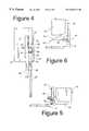
- FIG. 4additional detail of the mechanism which controls the opening and shutting door 21 is shown.
- a side panel 31 of door 21is connected to a carriage 30 by a spring 34 , a link 36 and a link 35 .
- door 21travels up and down parallel to a rail 50 .
- door 21is stopped by an abutment 32 ; however, carriage 30 continues upward, expanding spring 34 , until a gap 33 is completely closed.
- carriage 30continues moving upward, a pivot 39 connected to link 36 , and a pivot 40 connected to link 35 continue moving upward.
- a pivot 37 connected to link 36 and a pivot 38 connected to link 35cause door 21 to move towards carriage 30 . Therefore, as gap 33 is closed, links 35 and 36 translate the upward motion of carriage 30 into horizontal motion of door 21 .
- Door 21is thus brought snug against, and hence seals chamber 8 .
- spring 34compresses causing gap 33 to reappear and links 35 and 36 to straighten, thus moving door 21 horizontally away from chamber 8 .
- FIGS. 5 and 6show a block diagram of one possible implementation of an assembly for guiding the lowering and raising of support structure 43 .
- support structure 43 and cassette 16are shown lowered out of chamber 8 .
- a roller 44 connected to support structure 43is shown resting on an extension of a cam containing slot 46 within chamber 8 .
- a roller 45also connected to support structure 43 , is shown at a first end of a slot track 46 .
- support structure 43 and cassette 16are shown in the upright position within chamber 8 . In this position, wafers 10 are horizontal and are stacked so that they are ready to be accessed by semiconductor processing equipment 1 .
- roller 45is rolled to a second end of slot track 46 and roller 44 rests against a stop 49 . Stop 49 is an extension of the cam which contains slot 46 .
Landscapes
- Engineering & Computer Science (AREA)
- Physics & Mathematics (AREA)
- Condensed Matter Physics & Semiconductors (AREA)
- General Physics & Mathematics (AREA)
- Manufacturing & Machinery (AREA)
- Computer Hardware Design (AREA)
- Microelectronics & Electronic Packaging (AREA)
- Power Engineering (AREA)
- Robotics (AREA)
- Container, Conveyance, Adherence, Positioning, Of Wafer (AREA)
- Electrodes Of Semiconductors (AREA)
- Drying Of Semiconductors (AREA)
Abstract
Description
This application is a continuation of U.S. patent application Ser. No. 08/099,983 filed Jul. 30, 1993, now abandoned, which is a continuation of U.S. patent application Ser. No. 07/849,115, filed Mar. 10, 1992, now abandoned which is a divisional of U.S. patent application Ser. No. 07/511,481, filed Apr. 19, 1990, now U.S. Pat. No. 5,186,594.
The present invention relates to a front end loading interface used in the loading of workpieces in semiconductor processing equipment.
Semiconductor processing equipment often has a plurality of chambers in which processing occurs. Arm assemblies or other robotic devices are generally used to move workpieces, generally wafers from a wafer queuing station to various chambers for processing. When the processing is finished the wafer is returned to the queuing station. For an example of prior art processing equipment, see U.S. Pat. No. 4,715,921 issued to Maher et al. for a Ouad Processor.
Semiconductor processing is typically done in a vacuum. Therefore, a wafer queuing station into which is placed a cassette of wafers to be processed must be pumped down before the wafers may be accessed. This significantly increases the time the semiconductor processing equipment is idle while waiting for a cassette of processed wafers to be exchanged for a cassette of unprocessed wafers and subsequent pumping down of the wafer queuing station.
In accordance with the preferred embodiment of the present invention, a workpiece loading interface is presented for inclusion within a workpiece processing system. The workpiece loading interface includes two separate chambers. Each chamber may be separately pumped down. Thus, while a first cassette of workpieces, typically wafers, from a first chamber are being accessed, a second cassette of wafers may be loaded in the second chamber and the second chamber may then be pumped down. This can significantly increase throughput of wafers through the workpiece processing system.
In the preferred embodiment, each chamber is designed to minimize intrusion to a clean room. Thus a door to each chamber has a mechanism which, when opening the door, first moves the door slightly away from an opening in the chamber and then the door is moved down parallel to the chamber. After the door is opened, a cassette of wafers is lowered through the opening in a motion much like a drawbridge. The cassette of wafers is on a support with no side panels, facilitating the replacement of a cassette of processed wafers with a cassette of unprocessed wafers by an automated device. The cassette may be pivoted within the chamber when the position from which wafers are accessed from the cassette differs from the position from which the cassette is lowered out of the chamber.
FIG. 1 shows a top view of a block diagram of semiconductor processing equipment which includes two cassette load locks in accordance with the preferred embodiment of the present invention.
FIG. 2 shows a block diagram of a load lock which is part of the semiconductor processing equipment shown in FIG. 1 in accordance with the preferred embodiment of the present invention.
FIG. 3 shows a second block diagram of the load lock shown in FIG. 2 in accordance with the preferred embodiment of the present invention.
FIG. 4 shows another block diagram of the load lock shown in FIG. 2 in accordance with the preferred embodiment of the present invention.
FIG. 5 is a block diagram of a cassette wafer holder in a position extended out of the load lock shown in FIG. 2 in accordance with the preferred embodiment of the present invention.
FIG. 6 is a block diagram of the cassette wafer shown in FIG. 5 in an upright position within the load lock shown in FIG. 2 in accordance with the preferred embodiment of the present invention.
In FIG. 1, a top view of semiconductor processing equipment1 is shown. Semiconductor processing equipment1 may be used, for example, for etching wafers.
Semiconductor processing equipment1, includes, for example, aprocessing chamber 3, aprocessing chamber 4, aprocessing chamber 5 and aprocessing chamber 6. Acentral chamber 2 may be used to temporarily store wafers on robotic equipment7 when wafers are being moved to or from various of the processing chambers.
Semiconductor processing equipment also includes dual cassette load locks. Inchamber 8, awafer cassette 16 holdswafers 10. Inchamber 9, awafer cassette 17 holdswafers 11. Wafer tray17 pivots around apivot point 15. When wafers11 fromtray 17 are accessed by semiconductor processing equipment1 for processing,wafer tray 17 is flush against agate 13, as shown, and easily accessed by robotic equipment7 for transportation intocentral chamber 2. Whenwafer tray 17 is ready to be removed fromchamber 9,wafer tray 17 is pivoted back fromgate 13 in preparation for the opening ofchamber 9 and removal ofwafer tray 17.
Similarly, wafer tray16 pivots around apivot point 14. When wafers10 fromtray 16 are accessed by semiconductor processing equipment1 for processing,wafer tray 16 is flush against agate 12 and easily accessed by robotic equipment7 for transportation intocentral chamber 2. Whenwafer tray 16 is ready to be removed fromchamber 8,wafer tray 16 may be pivoted back anangle 18 fromgate 12, as shown, in preparation for the opening ofchamber 8 and removal ofwafer tray 16. In the preferred embodiment,angle 18 is about twenty-one degrees.
FIG. 2 shows a simplified block diagram front view ofwafer chamber 8. In the preferred embodiment, the volume ofchamber 8 is 46 liters. Adoor 21 is shown in a closed position.Door 21 includes anobservation window 22.Door 21 is opened and closed using a pneumatic actuator within arod 24. Magnets in the pneumatic actuator interface attract anouter ring 26.Outer ring 26 is connected todoor 21 through anassembly 23.
FIG. 3shows door 21 lowered into an open position. An opening25, for example may be fifteen inches high and ten and one half inches wide. By opening down, the intrusion ofdoor 21 into a clean room may be minimized. In the preferred embodiment the total intrusion is about one inch.
Oncedoor 21 is lowered,wafer tray 16, on asupport structure 43, may then be lowered out ofchamber 8, much like a draw bridge is lowered at a castle entrance.Wafer tray 16 may then be removed and a new wafer tray placed uponsupport structure 43.Support structure 43 is designed with a hollow bottom so that whendoor 21 is opened andwafer tray 16 is lowered, a laminar airflow may sweep downward throughwafers 10.
In FIG. 4, additional detail of the mechanism which controls the opening and shuttingdoor 21 is shown. Aside panel 31 ofdoor 21 is connected to acarriage 30 by aspring 34, alink 36 and alink 35. As controlled by the pneumatic actuator withinrod 24,door 21 travels up and down parallel to arail 50. When being closed,door 21 is stopped by anabutment 32; however,carriage 30 continues upward, expandingspring 34, until agap 33 is completely closed. Whilecarriage 30 continues moving upward, apivot 39 connected to link36, and apivot 40 connected to link35 continue moving upward. However apivot 37 connected to link36 and apivot 38 connected to link35cause door 21 to move towardscarriage 30. Therefore, asgap 33 is closed, links35 and36 translate the upward motion ofcarriage 30 into horizontal motion ofdoor 21.Door 21 is thus brought snug against, and hence sealschamber 8.
Whendoor 21 is opened,spring 34compresses causing gap 33 to reappear andlinks door 21 horizontally away fromchamber 8.
FIGS. 5 and 6 show a block diagram of one possible implementation of an assembly for guiding the lowering and raising ofsupport structure 43. In FIG. 5,support structure 43 andcassette 16 are shown lowered out ofchamber 8. Aroller 44 connected to supportstructure 43 is shown resting on an extension of acam containing slot 46 withinchamber 8. Aroller 45, also connected to supportstructure 43, is shown at a first end of aslot track 46.
In FIG. 6,support structure 43 andcassette 16 are shown in the upright position withinchamber 8. In this position,wafers 10 are horizontal and are stacked so that they are ready to be accessed by semiconductor processing equipment1. Whensupport structure 43 andcassette 16 are in the upright position,roller 45 is rolled to a second end ofslot track 46 androller 44 rests against astop 49.Stop 49 is an extension of the cam which containsslot 46.
Claims (9)
1. In a workpiece processing system comprising multiple vacuum processing chambers coupled to a central chamber, a method for loading workpieces into the central chamber, comprising the steps of:
providing dual workpiece load/unload chambers coupled to the central chamber, each having an opening for receiving workpieces held in a cassette and for forwarding the cassette of workpieces to the central chamber of the workpiece processing chamber for further transfer to one of the multiple vacuum chambers for processing:
providing a cassette support pivotally mounted within each of said load/unload chambers;
pivoting each cassette support to a first pivot position;
operating each cassette support to raise and lower a cassette of workpieces into and out of the opening of the respective load/unload chamber when in the first pivot position of the cassette support about a horizontal axis, and
thereafter pivoting each cassette to a second pivot position to position the cassette for forwarding of the workpieces to the central chamber from the second pivot position of the cassette support wherein pivoting occurs about a substantially vertical axis.
2. The method ofclaim 1 wherein the cassette support is vertically oriented and adjacent the opening for receiving workpieces when in the first pivot position and is vertically oriented and adjacent the opening for forwarding workpieces when in the second pivot position.
3. The method ofclaim 2 wherein when operating each cassette support to raise and lower, the cassette support lowers to a horizontally oriented position and raises to the vertically oriented position about a horizontal axis.
4. The method ofclaim 1 wherein the angle of pivoting about the substantially vertical axis between the first and second pivot position is about 21 degrees.
5. In a workpiece processing system comprising a central chamber connected to at least one processing chamber, a method for loading a workpiece into the central chamber, comprising the steps of:
providing dual workpiece load/unload chambers each coupled to the central chamber, the dual workpiece load/unload chambers each having a first opening for receiving a workpiece carrier and a second opening for forwarding a workpiece to the central chamber;
providing a workpiece carrier support pivotally mounted about a horizontal axis within each dual workpiece load/unload chamber to receive a workpiece carrier through the first opening;
within a first of the dual workpiece load/unload chambers:
pivoting the workpiece carrier support into a first pivot position when a first workpiece carrier is to be received through the first opening, the pivoting occurring in a first direction; and
pivoting the workpiece carrier support into a second pivot position when a workpiece is to be extracted from the first workpiece carrier and forwarded to the central chamber, the pivoting occurring in a second direction that is opposite the first direction; and
within a second of the dual workpiece load/unload chambers:
pivoting the workpiece carrier support into a first pivot position when a second workpiece carrier is to be received through the first opening, the pivoting occurring in the second direction; and
pivoting the workpiece carrier support into a second pivot position when a workpiece is to be extracted from the second workpiece carrier and forwarded to the central chamber, the pivoting occurring in the first direction;
wherein each pivoting step occurs about a substantially vertical axis.
6. The method ofclaim 5 wherein the workpiece carrier support is vertically oriented in both the first and second pivot positions.
7. The method ofclaim 5 wherein the angle of pivoting about the substantially vertical axis between the first and second pivot positions is about 21 degrees.
8. In a workpiece processing system comprising a central chamber connected to at least one processing chamber, a method for loading a workpiece into the central chamber, comprising the steps of:
providing a workpiece load chamber coupled to the central chamber and having an opening for receiving a workpiece carrier and for forwarding a workpiece from the workpiece carrier to the central chamber;
providing a single workpiece carrier support mounted for movement about a horizontal axis and a vertical axis within the workpiece load chamber for dual movement between lowered and raised positions and first and second pivot positions;
pivoting the workpiece carrier support to the first pivot position;
operating the workpiece carrier support to move between a first lower position to receive the workpiece carrier and a second raised position to move the received workpiece carrier through the opening and place the workpiece carrier within the load chamber when in the first pivot position; and
thereafter pivoting the workpiece carrier support to a second pivot position to forward a workpiece from the workpiece carrier to the central chamber;
wherein pivoting occurs about a substantially vertical axis.
9. The method ofclaim 8 wherein the angle of pivoting about the substantially vertical axis between the first and second pivot positions is about 21 degrees.
Priority Applications (2)
| Application Number | Priority Date | Filing Date | Title |
|---|---|---|---|
| US08/813,480US6454519B1 (en) | 1990-04-19 | 1997-03-07 | Dual cassette load lock |
| US10/223,539US6599076B2 (en) | 1990-04-19 | 2002-08-19 | Dual cassette load lock |
Applications Claiming Priority (4)
| Application Number | Priority Date | Filing Date | Title |
|---|---|---|---|
| US07/511,481US5186594A (en) | 1990-04-19 | 1990-04-19 | Dual cassette load lock |
| US84911592A | 1992-03-10 | 1992-03-10 | |
| US9998393A | 1993-07-30 | 1993-07-30 | |
| US08/813,480US6454519B1 (en) | 1990-04-19 | 1997-03-07 | Dual cassette load lock |
Related Parent Applications (1)
| Application Number | Title | Priority Date | Filing Date |
|---|---|---|---|
| US9998393AContinuation | 1990-04-19 | 1993-07-30 |
Related Child Applications (1)
| Application Number | Title | Priority Date | Filing Date |
|---|---|---|---|
| US10/223,539DivisionUS6599076B2 (en) | 1990-04-19 | 2002-08-19 | Dual cassette load lock |
Publications (1)
| Publication Number | Publication Date |
|---|---|
| US6454519B1true US6454519B1 (en) | 2002-09-24 |
Family
ID=24035085
Family Applications (7)
| Application Number | Title | Priority Date | Filing Date |
|---|---|---|---|
| US07/511,481Expired - LifetimeUS5186594A (en) | 1990-04-19 | 1990-04-19 | Dual cassette load lock |
| US08/700,267Expired - Fee RelatedUS5769588A (en) | 1990-04-19 | 1996-08-20 | Dual cassette load lock |
| US08/813,480Expired - Fee RelatedUS6454519B1 (en) | 1990-04-19 | 1997-03-07 | Dual cassette load lock |
| US09/070,854Expired - Fee RelatedUS6454508B2 (en) | 1990-04-19 | 1998-05-01 | Dual cassette load lock |
| US10/223,540AbandonedUS20030002960A1 (en) | 1990-04-19 | 2002-08-19 | Dual cassette load lock |
| US10/223,539Expired - Fee RelatedUS6599076B2 (en) | 1990-04-19 | 2002-08-19 | Dual cassette load lock |
| US11/410,797AbandonedUS20060245854A1 (en) | 1990-04-19 | 2006-04-24 | Dual cassette load lock |
Family Applications Before (2)
| Application Number | Title | Priority Date | Filing Date |
|---|---|---|---|
| US07/511,481Expired - LifetimeUS5186594A (en) | 1990-04-19 | 1990-04-19 | Dual cassette load lock |
| US08/700,267Expired - Fee RelatedUS5769588A (en) | 1990-04-19 | 1996-08-20 | Dual cassette load lock |
Family Applications After (4)
| Application Number | Title | Priority Date | Filing Date |
|---|---|---|---|
| US09/070,854Expired - Fee RelatedUS6454508B2 (en) | 1990-04-19 | 1998-05-01 | Dual cassette load lock |
| US10/223,540AbandonedUS20030002960A1 (en) | 1990-04-19 | 2002-08-19 | Dual cassette load lock |
| US10/223,539Expired - Fee RelatedUS6599076B2 (en) | 1990-04-19 | 2002-08-19 | Dual cassette load lock |
| US11/410,797AbandonedUS20060245854A1 (en) | 1990-04-19 | 2006-04-24 | Dual cassette load lock |
Country Status (5)
| Country | Link |
|---|---|
| US (7) | US5186594A (en) |
| EP (1) | EP0452939B1 (en) |
| JP (1) | JP3088123B2 (en) |
| KR (1) | KR100272890B1 (en) |
| DE (1) | DE69132457T2 (en) |
Cited By (32)
| Publication number | Priority date | Publication date | Assignee | Title |
|---|---|---|---|---|
| US20030121534A1 (en)* | 1999-11-02 | 2003-07-03 | Biberger Maximilian Albert | Method and apparatus for supercritical processing of multiple workpieces |
| US6871656B2 (en) | 1997-05-27 | 2005-03-29 | Tokyo Electron Limited | Removal of photoresist and photoresist residue from semiconductors using supercritical carbon dioxide process |
| US6926798B2 (en) | 1999-11-02 | 2005-08-09 | Tokyo Electron Limited | Apparatus for supercritical processing of a workpiece |
| US7001468B1 (en) | 2002-02-15 | 2006-02-21 | Tokyo Electron Limited | Pressure energized pressure vessel opening and closing device and method of providing therefor |
| US7021635B2 (en) | 2003-02-06 | 2006-04-04 | Tokyo Electron Limited | Vacuum chuck utilizing sintered material and method of providing thereof |
| US7077917B2 (en) | 2003-02-10 | 2006-07-18 | Tokyo Electric Limited | High-pressure processing chamber for a semiconductor wafer |
| US7140393B2 (en) | 2004-12-22 | 2006-11-28 | Tokyo Electron Limited | Non-contact shuttle valve for flow diversion in high pressure systems |
| US7163380B2 (en) | 2003-07-29 | 2007-01-16 | Tokyo Electron Limited | Control of fluid flow in the processing of an object with a fluid |
| US7186093B2 (en) | 2004-10-05 | 2007-03-06 | Tokyo Electron Limited | Method and apparatus for cooling motor bearings of a high pressure pump |
| US20070116545A1 (en)* | 2005-11-21 | 2007-05-24 | Applied Materials, Inc. | Apparatus and methods for a substrate carrier having an inflatable seal |
| US7225820B2 (en) | 2003-02-10 | 2007-06-05 | Tokyo Electron Limited | High-pressure processing chamber for a semiconductor wafer |
| US7250374B2 (en) | 2004-06-30 | 2007-07-31 | Tokyo Electron Limited | System and method for processing a substrate using supercritical carbon dioxide processing |
| US7255772B2 (en) | 2000-07-26 | 2007-08-14 | Tokyo Electron Limited | High pressure processing chamber for semiconductor substrate |
| US7270137B2 (en) | 2003-04-28 | 2007-09-18 | Tokyo Electron Limited | Apparatus and method of securing a workpiece during high-pressure processing |
| US7291565B2 (en) | 2005-02-15 | 2007-11-06 | Tokyo Electron Limited | Method and system for treating a substrate with a high pressure fluid using fluorosilicic acid |
| US7307019B2 (en) | 2004-09-29 | 2007-12-11 | Tokyo Electron Limited | Method for supercritical carbon dioxide processing of fluoro-carbon films |
| US7380984B2 (en) | 2005-03-28 | 2008-06-03 | Tokyo Electron Limited | Process flow thermocouple |
| US7387868B2 (en) | 2002-03-04 | 2008-06-17 | Tokyo Electron Limited | Treatment of a dielectric layer using supercritical CO2 |
| US7434590B2 (en) | 2004-12-22 | 2008-10-14 | Tokyo Electron Limited | Method and apparatus for clamping a substrate in a high pressure processing system |
| US7435447B2 (en) | 2005-02-15 | 2008-10-14 | Tokyo Electron Limited | Method and system for determining flow conditions in a high pressure processing system |
| US7491036B2 (en) | 2004-11-12 | 2009-02-17 | Tokyo Electron Limited | Method and system for cooling a pump |
| US7494107B2 (en) | 2005-03-30 | 2009-02-24 | Supercritical Systems, Inc. | Gate valve for plus-atmospheric pressure semiconductor process vessels |
| US7524383B2 (en) | 2005-05-25 | 2009-04-28 | Tokyo Electron Limited | Method and system for passivating a processing chamber |
| US7611319B2 (en) | 2004-06-16 | 2009-11-03 | Applied Materials, Inc. | Methods and apparatus for identifying small lot size substrate carriers |
| US7767145B2 (en) | 2005-03-28 | 2010-08-03 | Toyko Electron Limited | High pressure fourier transform infrared cell |
| US7789971B2 (en) | 2005-05-13 | 2010-09-07 | Tokyo Electron Limited | Treatment of substrate using functionalizing agent in supercritical carbon dioxide |
| US20140346724A1 (en)* | 2011-09-19 | 2014-11-27 | Oerlikon Trading Ag, Trubbach | Carousel carrier for a vacuum treatment installation |
| US9997384B2 (en)* | 2011-12-01 | 2018-06-12 | Taiwan Semiconductor Manufacturing Company, Ltd. | Methods for transporting wafers between wafer holders and chambers |
| US10115616B2 (en) | 2013-07-18 | 2018-10-30 | Applied Materials, Inc. | Carrier adapter insert apparatus and carrier adapter insert detection methods |
| US10192765B2 (en) | 2013-08-12 | 2019-01-29 | Applied Materials, Inc. | Substrate processing systems, apparatus, and methods with factory interface environmental controls |
| US10359743B2 (en) | 2014-11-25 | 2019-07-23 | Applied Materials, Inc. | Substrate processing systems, apparatus, and methods with substrate carrier and purge chamber environmental controls |
| WO2019154462A1 (en)* | 2018-02-07 | 2019-08-15 | Uwe Beier | Load lock for a substrate container and device having a load lock |
Families Citing this family (120)
| Publication number | Priority date | Publication date | Assignee | Title |
|---|---|---|---|---|
| US5186594A (en)* | 1990-04-19 | 1993-02-16 | Applied Materials, Inc. | Dual cassette load lock |
| KR0162102B1 (en)* | 1991-05-29 | 1999-02-01 | 이노우에 아키라 | Semiconductor manufacturing device |
| JP2598353B2 (en)* | 1991-12-04 | 1997-04-09 | アネルバ株式会社 | Substrate processing device, substrate transfer device, and substrate replacement method |
| JP2751975B2 (en)* | 1991-12-20 | 1998-05-18 | 株式会社日立製作所 | Load lock chamber of semiconductor processing equipment |
| US5372836A (en)* | 1992-03-27 | 1994-12-13 | Tokyo Electron Limited | Method of forming polycrystalling silicon film in process of manufacturing LCD |
| US5395198A (en)* | 1992-06-19 | 1995-03-07 | International Business Machines Corporation | Vacuum loading chuck and fixture for flexible printed circuit panels |
| US5534072A (en)* | 1992-06-24 | 1996-07-09 | Anelva Corporation | Integrated module multi-chamber CVD processing system and its method for processing subtrates |
| US5482607A (en)* | 1992-09-21 | 1996-01-09 | Nissin Electric Co., Ltd. | Film forming apparatus |
| CN1088002A (en)* | 1992-11-16 | 1994-06-15 | 东京电子株式会社 | Make the method and apparatus of liquid crystal display substrate and evaluating semiconductor crystals |
| US5387067A (en)* | 1993-01-14 | 1995-02-07 | Applied Materials, Inc. | Direct load/unload semiconductor wafer cassette apparatus and transfer system |
| KR100261532B1 (en)* | 1993-03-14 | 2000-07-15 | 야마시타 히데나리 | Multi-chamber system with workpiece conveying device |
| US5527390A (en)* | 1993-03-19 | 1996-06-18 | Tokyo Electron Kabushiki | Treatment system including a plurality of treatment apparatus |
| US5478455A (en)* | 1993-09-17 | 1995-12-26 | Varian Associates, Inc. | Method for controlling a collimated sputtering source |
| US6447232B1 (en) | 1994-04-28 | 2002-09-10 | Semitool, Inc. | Semiconductor wafer processing apparatus having improved wafer input/output handling system |
| US5664337A (en)* | 1996-03-26 | 1997-09-09 | Semitool, Inc. | Automated semiconductor processing systems |
| US5544421A (en)* | 1994-04-28 | 1996-08-13 | Semitool, Inc. | Semiconductor wafer processing system |
| US6712577B2 (en)* | 1994-04-28 | 2004-03-30 | Semitool, Inc. | Automated semiconductor processing system |
| AU2368495A (en)* | 1994-04-28 | 1995-11-29 | Semitool, Incorporated | Semiconductor processing system with wafer container docking and loading station |
| US6833035B1 (en) | 1994-04-28 | 2004-12-21 | Semitool, Inc. | Semiconductor processing system with wafer container docking and loading station |
| US5538385A (en)* | 1994-06-24 | 1996-07-23 | Kensington Laboratories, Inc. | Specimen carrier holder and method of operating it |
| US5486080A (en)* | 1994-06-30 | 1996-01-23 | Diamond Semiconductor Group, Inc. | High speed movement of workpieces in vacuum processing |
| US5522955A (en)* | 1994-07-07 | 1996-06-04 | Brodd; Ralph J. | Process and apparatus for producing thin lithium coatings on electrically conductive foil for use in solid state rechargeable electrochemical cells |
| US5525024A (en)* | 1994-08-17 | 1996-06-11 | Applied Materials, Inc. | Cassette loader having compound translational motion |
| US5563095A (en)* | 1994-12-01 | 1996-10-08 | Frey; Jeffrey | Method for manufacturing semiconductor devices |
| EP0735573B1 (en)* | 1995-03-28 | 2004-09-08 | BROOKS Automation GmbH | Loading and unloading station for semiconductor treatment installations |
| DE19542646C2 (en)* | 1995-03-28 | 2003-04-30 | Brooks Automation Gmbh | Loading and unloading station for semiconductor processing systems |
| KR0165484B1 (en) | 1995-11-28 | 1999-02-01 | 김광호 | Tantalum oxide film deposition forming method and apparatus |
| US6555394B2 (en) | 1995-11-28 | 2003-04-29 | Samsung Electronics Co., Ltd. | Methods of fabricating capacitors including Ta2O5 layers in a chamber including changing a Ta2O5 layer to heater separation or chamber pressure |
| US6723174B2 (en) | 1996-03-26 | 2004-04-20 | Semitool, Inc. | Automated semiconductor processing system |
| US6279724B1 (en) | 1997-12-19 | 2001-08-28 | Semitoll Inc. | Automated semiconductor processing system |
| US6942738B1 (en) | 1996-07-15 | 2005-09-13 | Semitool, Inc. | Automated semiconductor processing system |
| US6105534A (en)* | 1996-05-31 | 2000-08-22 | Ipec Precision, Inc. | Apparatus for plasma jet treatment of substrates |
| US6645355B2 (en) | 1996-07-15 | 2003-11-11 | Semitool, Inc. | Semiconductor processing apparatus having lift and tilt mechanism |
| US6203582B1 (en)* | 1996-07-15 | 2001-03-20 | Semitool, Inc. | Modular semiconductor workpiece processing tool |
| US6091498A (en)* | 1996-07-15 | 2000-07-18 | Semitool, Inc. | Semiconductor processing apparatus having lift and tilt mechanism |
| US6672820B1 (en) | 1996-07-15 | 2004-01-06 | Semitool, Inc. | Semiconductor processing apparatus having linear conveyer system |
| JP3509410B2 (en) | 1996-08-30 | 2004-03-22 | 東京エレクトロン株式会社 | Cassette chamber |
| TW331550B (en)* | 1996-08-14 | 1998-05-11 | Tokyo Electron Co Ltd | The cassette receiving room |
| TW344847B (en)* | 1996-08-29 | 1998-11-11 | Tokyo Electron Co Ltd | Substrate treatment system, substrate transfer system, and substrate transfer method |
| JPH10107122A (en)* | 1996-10-01 | 1998-04-24 | Tokyo Electron Ltd | Device for carrying in cassette for substrate to be processed |
| JPH10139159A (en)* | 1996-11-13 | 1998-05-26 | Tokyo Electron Ltd | Cassette chamber and cassette carrying-in and out mechanism |
| US5961269A (en) | 1996-11-18 | 1999-10-05 | Applied Materials, Inc. | Three chamber load lock apparatus |
| US5905302A (en)* | 1996-11-18 | 1999-05-18 | Applied Materials, Inc. | Loadlock cassette with wafer support rails |
| JPH10147432A (en)* | 1996-11-20 | 1998-06-02 | Tokyo Electron Ltd | Cassette chamber |
| US6068668A (en)* | 1997-03-31 | 2000-05-30 | Motorola, Inc. | Process for forming a semiconductor device |
| US5837059A (en)* | 1997-07-11 | 1998-11-17 | Brooks Automation, Inc. | Automatic positive pressure seal access door |
| US6152680A (en)* | 1997-08-26 | 2000-11-28 | Daitron, Inc. | Wafer cassette rotation mechanism |
| US6106213A (en)* | 1998-02-27 | 2000-08-22 | Pri Automation, Inc. | Automated door assembly for use in semiconductor wafer manufacturing |
| TWI223678B (en)* | 1998-03-20 | 2004-11-11 | Semitool Inc | Process for applying a metal structure to a workpiece, the treated workpiece and a solution for electroplating copper |
| US6565729B2 (en)* | 1998-03-20 | 2003-05-20 | Semitool, Inc. | Method for electrochemically depositing metal on a semiconductor workpiece |
| US6497801B1 (en) | 1998-07-10 | 2002-12-24 | Semitool Inc | Electroplating apparatus with segmented anode array |
| US6375746B1 (en) | 1998-07-10 | 2002-04-23 | Novellus Systems, Inc. | Wafer processing architecture including load locks |
| US6431807B1 (en) | 1998-07-10 | 2002-08-13 | Novellus Systems, Inc. | Wafer processing architecture including single-wafer load lock with cooling unit |
| US6350321B1 (en)* | 1998-12-08 | 2002-02-26 | International Business Machines Corporation | UHV horizontal hot wall cluster CVD/growth design |
| US7077159B1 (en)* | 1998-12-23 | 2006-07-18 | Applied Materials, Inc. | Processing apparatus having integrated pumping system |
| US6358128B1 (en)* | 1999-03-05 | 2002-03-19 | Ebara Corporation | Polishing apparatus |
| US6042324A (en)* | 1999-03-26 | 2000-03-28 | Asm America, Inc. | Multi-stage single-drive FOUP door system |
| US7189318B2 (en)* | 1999-04-13 | 2007-03-13 | Semitool, Inc. | Tuning electrodes used in a reactor for electrochemically processing a microelectronic workpiece |
| US7264698B2 (en)* | 1999-04-13 | 2007-09-04 | Semitool, Inc. | Apparatus and methods for electrochemical processing of microelectronic workpieces |
| US6368475B1 (en)* | 2000-03-21 | 2002-04-09 | Semitool, Inc. | Apparatus for electrochemically processing a microelectronic workpiece |
| US7020537B2 (en)* | 1999-04-13 | 2006-03-28 | Semitool, Inc. | Tuning electrodes used in a reactor for electrochemically processing a microelectronic workpiece |
| US7438788B2 (en)* | 1999-04-13 | 2008-10-21 | Semitool, Inc. | Apparatus and methods for electrochemical processing of microelectronic workpieces |
| US7160421B2 (en)* | 1999-04-13 | 2007-01-09 | Semitool, Inc. | Turning electrodes used in a reactor for electrochemically processing a microelectronic workpiece |
| US7351315B2 (en) | 2003-12-05 | 2008-04-01 | Semitool, Inc. | Chambers, systems, and methods for electrochemically processing microfeature workpieces |
| US7585398B2 (en)* | 1999-04-13 | 2009-09-08 | Semitool, Inc. | Chambers, systems, and methods for electrochemically processing microfeature workpieces |
| US7351314B2 (en) | 2003-12-05 | 2008-04-01 | Semitool, Inc. | Chambers, systems, and methods for electrochemically processing microfeature workpieces |
| US20030038035A1 (en)* | 2001-05-30 | 2003-02-27 | Wilson Gregory J. | Methods and systems for controlling current in electrochemical processing of microelectronic workpieces |
| US6916412B2 (en) | 1999-04-13 | 2005-07-12 | Semitool, Inc. | Adaptable electrochemical processing chamber |
| TWI226387B (en)* | 1999-04-13 | 2005-01-11 | Semitool Inc | Workpiece processor having processing chamber with improved processing fluid flow |
| TW469483B (en)* | 1999-04-19 | 2001-12-21 | Applied Materials Inc | Method and apparatus for aligning a cassette |
| US6763281B2 (en) | 1999-04-19 | 2004-07-13 | Applied Materials, Inc | Apparatus for alignment of automated workpiece handling systems |
| US6612797B1 (en)* | 1999-05-18 | 2003-09-02 | Asyst Technologies, Inc. | Cassette buffering within a minienvironment |
| US6428262B1 (en)* | 1999-08-11 | 2002-08-06 | Proteros, Llc | Compact load lock system for ion beam processing of foups |
| US6318384B1 (en)* | 1999-09-24 | 2001-11-20 | Applied Materials, Inc. | Self cleaning method of forming deep trenches in silicon substrates |
| US8348583B2 (en)* | 1999-10-19 | 2013-01-08 | Rorze Corporation | Container and loader for substrate |
| AU2913901A (en)* | 2000-01-03 | 2001-07-16 | Skion Corporation | Multi wafer introduction/single wafer conveyor mode processing system and methodof processing wafers using the same |
| EP1126508A3 (en)* | 2000-02-16 | 2005-03-30 | Applied Materials, Inc. | Processing apparatus having integrated pumping system |
| US20050183959A1 (en)* | 2000-04-13 | 2005-08-25 | Wilson Gregory J. | Tuning electrodes used in a reactor for electrochemically processing a microelectric workpiece |
| WO2001090434A2 (en)* | 2000-05-24 | 2001-11-29 | Semitool, Inc. | Tuning electrodes used in a reactor for electrochemically processing a microelectronic workpiece |
| US6977014B1 (en) | 2000-06-02 | 2005-12-20 | Novellus Systems, Inc. | Architecture for high throughput semiconductor processing applications |
| US6364593B1 (en)* | 2000-06-06 | 2002-04-02 | Brooks Automation | Material transport system |
| US6860965B1 (en) | 2000-06-23 | 2005-03-01 | Novellus Systems, Inc. | High throughput architecture for semiconductor processing |
| JP2004524673A (en) | 2000-07-07 | 2004-08-12 | セミトゥール・インコーポレイテッド | Automatic processing system |
| WO2002004774A2 (en)* | 2000-07-07 | 2002-01-17 | Applied Materials, Inc. | Automatic door opener |
| US6632068B2 (en)* | 2000-09-27 | 2003-10-14 | Asm International N.V. | Wafer handling system |
| US7090751B2 (en) | 2001-08-31 | 2006-08-15 | Semitool, Inc. | Apparatus and methods for electrochemical processing of microelectronic workpieces |
| US20030194673A1 (en)* | 2002-04-15 | 2003-10-16 | Yoo Woo Sik | Batch furnace isolation gate |
| US7114903B2 (en)* | 2002-07-16 | 2006-10-03 | Semitool, Inc. | Apparatuses and method for transferring and/or pre-processing microelectronic workpieces |
| US6869263B2 (en) | 2002-07-22 | 2005-03-22 | Brooks Automation, Inc. | Substrate loading and unloading station with buffer |
| US7677859B2 (en) | 2002-07-22 | 2010-03-16 | Brooks Automation, Inc. | Substrate loading and uploading station with buffer |
| DE10238165B3 (en)* | 2002-08-15 | 2004-03-25 | Hans-Heinz Helge | Elongated roller shutter profile made of plastic or metal for swimming pool covers |
| US20040108212A1 (en)* | 2002-12-06 | 2004-06-10 | Lyndon Graham | Apparatus and methods for transferring heat during chemical processing of microelectronic workpieces |
| US6748293B1 (en) | 2003-03-24 | 2004-06-08 | Varian Semiconductor Equipment Associates, Inc. | Methods and apparatus for high speed object handling |
| US20050035514A1 (en)* | 2003-08-11 | 2005-02-17 | Supercritical Systems, Inc. | Vacuum chuck apparatus and method for holding a wafer during high pressure processing |
| US20050067002A1 (en)* | 2003-09-25 | 2005-03-31 | Supercritical Systems, Inc. | Processing chamber including a circulation loop integrally formed in a chamber housing |
| US7500822B2 (en)* | 2004-04-09 | 2009-03-10 | Edwards Vacuum, Inc. | Combined vacuum pump load-lock assembly |
| TWI390102B (en)* | 2004-08-13 | 2013-03-21 | Oc Oerlikon Balzers Ag | Vacuum sluice |
| US20060065189A1 (en)* | 2004-09-30 | 2006-03-30 | Darko Babic | Method and system for homogenization of supercritical fluid in a high pressure processing system |
| US20060065288A1 (en)* | 2004-09-30 | 2006-03-30 | Darko Babic | Supercritical fluid processing system having a coating on internal members and a method of using |
| US20060102204A1 (en)* | 2004-11-12 | 2006-05-18 | Tokyo Electron Limited | Method for removing a residue from a substrate using supercritical carbon dioxide processing |
| US20060102208A1 (en)* | 2004-11-12 | 2006-05-18 | Tokyo Electron Limited | System for removing a residue from a substrate using supercritical carbon dioxide processing |
| US20060102591A1 (en)* | 2004-11-12 | 2006-05-18 | Tokyo Electron Limited | Method and system for treating a substrate using a supercritical fluid |
| US20060102590A1 (en)* | 2004-11-12 | 2006-05-18 | Tokyo Electron Limited | Method for treating a substrate with a high pressure fluid using a preoxide-based process chemistry |
| US20060130966A1 (en)* | 2004-12-20 | 2006-06-22 | Darko Babic | Method and system for flowing a supercritical fluid in a high pressure processing system |
| US20060135047A1 (en)* | 2004-12-22 | 2006-06-22 | Alexei Sheydayi | Method and apparatus for clamping a substrate in a high pressure processing system |
| US20060134332A1 (en)* | 2004-12-22 | 2006-06-22 | Darko Babic | Precompressed coating of internal members in a supercritical fluid processing system |
| US20060180572A1 (en)* | 2005-02-15 | 2006-08-17 | Tokyo Electron Limited | Removal of post etch residue for a substrate with open metal surfaces |
| US20060180174A1 (en)* | 2005-02-15 | 2006-08-17 | Tokyo Electron Limited | Method and system for treating a substrate with a high pressure fluid using a peroxide-based process chemistry in conjunction with an initiator |
| US20060225772A1 (en)* | 2005-03-29 | 2006-10-12 | Jones William D | Controlled pressure differential in a high-pressure processing chamber |
| US20060226117A1 (en)* | 2005-03-29 | 2006-10-12 | Bertram Ronald T | Phase change based heating element system and method |
| US20060255012A1 (en)* | 2005-05-10 | 2006-11-16 | Gunilla Jacobson | Removal of particles from substrate surfaces using supercritical processing |
| US20070012337A1 (en)* | 2005-07-15 | 2007-01-18 | Tokyo Electron Limited | In-line metrology for supercritical fluid processing |
| KR100909494B1 (en)* | 2006-05-11 | 2009-07-27 | 도쿄엘렉트론가부시키가이샤 | Processing equipment |
| KR101659733B1 (en)* | 2009-12-28 | 2016-09-26 | 주식회사 테스 | Substrate treating apparatus |
| US20120288355A1 (en)* | 2011-05-11 | 2012-11-15 | Ming-Teng Hsieh | Method for storing wafers |
| JP6106176B2 (en)* | 2011-09-14 | 2017-03-29 | ブルックス オートメーション インコーポレイテッド | Road station |
| US9530675B2 (en) | 2012-09-19 | 2016-12-27 | Stmicroelectronics Pte Ltd | Wafer handling station including cassette members with lateral wafer confining brackets and associated methods |
| KR20180045316A (en)* | 2016-10-25 | 2018-05-04 | 삼성전자주식회사 | Equipment front end module and semiconductor manufacturing apparatus including the same |
| CN108538692B (en)* | 2017-03-02 | 2020-06-19 | 北京北方华创微电子装备有限公司 | Lifting door device and wafer transmission system |
| US12400894B2 (en) | 2019-02-19 | 2025-08-26 | Veeco Instruments Inc. | Automated batch production thin film deposition systems and methods of using the same |
Citations (27)
| Publication number | Priority date | Publication date | Assignee | Title |
|---|---|---|---|---|
| US2224479A (en)* | 1939-06-22 | 1940-12-10 | Marion S Jones | Ice handling apparatus |
| US3749383A (en)* | 1971-04-29 | 1973-07-31 | Rca Corp | Apparatus for processing semiconductor devices |
| US4448149A (en)* | 1982-10-12 | 1984-05-15 | International Business Machines Corporation | Apparatus for removably mounting and supplying mechanical and electrical energy to a vacuum chamber substrate holder |
| JPS60109218A (en) | 1983-11-18 | 1985-06-14 | Hitachi Ltd | Molecular beam epitaxial growth equipment |
| US4592306A (en)* | 1983-12-05 | 1986-06-03 | Pilkington Brothers P.L.C. | Apparatus for the deposition of multi-layer coatings |
| JPS61129881A (en) | 1984-11-28 | 1986-06-17 | Sanyo Electric Co Ltd | Photovoltaic device |
| JPS61282224A (en)* | 1985-06-04 | 1986-12-12 | Mitsubishi Electric Corp | Transport device loading/unloading device |
| US4640223A (en)* | 1984-07-24 | 1987-02-03 | Dozier Alfred R | Chemical vapor deposition reactor |
| JPS62139340A (en) | 1985-12-13 | 1987-06-23 | Hitachi Ltd | Wafer transfer device |
| JPS62154749A (en) | 1985-12-27 | 1987-07-09 | Hitachi Ltd | processing equipment |
| WO1987006561A1 (en)* | 1986-04-28 | 1987-11-05 | Varian Associates, Inc. | Modular semiconductor wafer transport and processing system |
| JPS62290616A (en) | 1986-06-05 | 1987-12-17 | Tokyo Electron Ltd | Wafer conveying mechanism |
| US4715921A (en)* | 1986-10-24 | 1987-12-29 | General Signal Corporation | Quad processor |
| US4764076A (en)* | 1986-04-17 | 1988-08-16 | Varian Associates, Inc. | Valve incorporating wafer handling arm |
| US4776744A (en)* | 1985-09-09 | 1988-10-11 | Applied Materials, Inc. | Systems and methods for wafer handling in semiconductor process equipment |
| JPH01166534A (en) | 1987-12-23 | 1989-06-30 | Hitachi Ltd | Workpiece storage support mechanism |
| US4851101A (en)* | 1987-09-18 | 1989-07-25 | Varian Associates, Inc. | Sputter module for modular wafer processing machine |
| US4851018A (en)* | 1986-11-28 | 1989-07-25 | Commissariat A L'energie Atomique | Installation for the storage and transfer of objects in a very clean atmosphere |
| JPH01251734A (en) | 1988-03-31 | 1989-10-06 | Teru Barian Kk | Semiconductor manufacturing apparatus |
| JPH01253237A (en) | 1988-03-31 | 1989-10-09 | Anelva Corp | Vacuum processor |
| EP0343530A2 (en) | 1988-05-24 | 1989-11-29 | Balzers Aktiengesellschaft | Vacuum installation |
| US4891488A (en)* | 1987-07-16 | 1990-01-02 | Texas Instruments Incorporated | Processing apparatus and method |
| US4951601A (en)* | 1986-12-19 | 1990-08-28 | Applied Materials, Inc. | Multi-chamber integrated process system |
| US4963069A (en)* | 1986-11-06 | 1990-10-16 | Meissner & Wurst Gmbh & Co. | Container for the handling of semiconductor devices and process for particle-free transfer |
| US4966519A (en)* | 1985-10-24 | 1990-10-30 | Texas Instruments Incorporated | Integrated circuit processing system |
| US4969790A (en)* | 1987-08-12 | 1990-11-13 | Leybold Aktiengesellschaft | Apparatus on the carousel principle for the coating of substrates |
| US5064337A (en)* | 1988-07-19 | 1991-11-12 | Tokyo Electron Limited | Handling apparatus for transferring carriers and a method of transferring carriers |
Family Cites Families (28)
| Publication number | Priority date | Publication date | Assignee | Title |
|---|---|---|---|---|
| US3656454A (en)* | 1970-11-23 | 1972-04-18 | Air Reduction | Vacuum coating apparatus |
| JPS5730341A (en)* | 1980-07-30 | 1982-02-18 | Anelva Corp | Substrate processing device |
| EP0068060A1 (en)* | 1981-06-25 | 1983-01-05 | S.A.R.L. Commodore International | Opening and closing commanding device for tight doors, particularly of autoclaves |
| DE3224803A1 (en)* | 1982-07-02 | 1984-01-05 | Heckmann, Klaus, Prof. Dr., 8400 Regensburg | METHOD FOR SELECTIVE SEPARATION OF PLUTONIUM FROM URANIUM AND OTHER METALS |
| JPS59191342A (en)* | 1983-04-15 | 1984-10-30 | Hitachi Ltd | semiconductor manufacturing equipment |
| JPS59200433A (en)* | 1983-04-28 | 1984-11-13 | Hitachi Electronics Eng Co Ltd | Loading method of chemical vapor deposition device |
| US4636128A (en)* | 1984-08-30 | 1987-01-13 | Texas Instruments Incorporated | Semiconductor slice cassette transport unit |
| US4668365A (en)* | 1984-10-25 | 1987-05-26 | Applied Materials, Inc. | Apparatus and method for magnetron-enhanced plasma-assisted chemical vapor deposition |
| FR2573908B1 (en)* | 1984-11-26 | 1986-12-26 | Cogema | DEVICE FOR TRANSFERRING DOUBLE SEALED BARRIER BETWEEN A CONTAINER AND A CONTAINMENT ENCLOSURE |
| JPS61291032A (en)* | 1985-06-17 | 1986-12-20 | Fujitsu Ltd | vacuum equipment |
| JPS6215479A (en)* | 1985-07-15 | 1987-01-23 | Komatsu Ltd | Auto tracking distance measuring device |
| US4765767A (en)* | 1985-08-01 | 1988-08-23 | Bic Corporation | Snap-on clip for elongated instruments |
| JPS62282224A (en) | 1986-05-30 | 1987-12-08 | Tokyo Keiki Co Ltd | Rotation detector |
| US4747577A (en)* | 1986-07-23 | 1988-05-31 | The Boc Group, Inc. | Gate valve with magnetic closure for use with vacuum equipment |
| US4721282A (en)* | 1986-12-16 | 1988-01-26 | Lam Research Corporation | Vacuum chamber gate valve |
| DE3704505A1 (en)* | 1987-02-13 | 1988-08-25 | Leybold Ag | INSERT UNIT FOR VACUUM SYSTEMS |
| JPH01186621A (en)* | 1987-07-16 | 1989-07-26 | Texas Instr Inc <Ti> | Apparatus and method for processing |
| US4832527A (en)* | 1987-09-29 | 1989-05-23 | Bachmann Company, Inc. | Vertically reciprocable gates for the control of a liquid media |
| US4859137A (en)* | 1987-10-21 | 1989-08-22 | Asyst Technologies | Apparatus for transporting a holder between a port opening of a standardized mechanical interface system and a loading and unloading station |
| JP2505011B2 (en)* | 1987-12-23 | 1996-06-05 | 松下電工株式会社 | Electromagnetic device of circuit breaker |
| JPH01212755A (en)* | 1988-02-18 | 1989-08-25 | Nissin Electric Co Ltd | Ion treatment equipment |
| JPH0237742A (en)* | 1988-07-28 | 1990-02-07 | Nec Corp | Semiconductor device manufacturing equipment |
| US5002255A (en)* | 1989-03-03 | 1991-03-26 | Irie Koken Kabushiki Kaisha | Non-sliding gate valve for high vacuum use |
| US5186594A (en)* | 1990-04-19 | 1993-02-16 | Applied Materials, Inc. | Dual cassette load lock |
| KR960002534A (en)* | 1994-06-07 | 1996-01-26 | 이노우에 아키라 | Pressure reducing and atmospheric pressure treatment device |
| US6106213A (en)* | 1998-02-27 | 2000-08-22 | Pri Automation, Inc. | Automated door assembly for use in semiconductor wafer manufacturing |
| WO2002004774A2 (en)* | 2000-07-07 | 2002-01-17 | Applied Materials, Inc. | Automatic door opener |
| US6799394B2 (en)* | 2002-01-18 | 2004-10-05 | Shen Tsung-Lin | Apparatus for sealing a vacuum chamber |
- 1990
- 1990-04-19USUS07/511,481patent/US5186594A/ennot_activeExpired - Lifetime
- 1991
- 1991-04-17JPJP03085141Apatent/JP3088123B2/ennot_activeExpired - Fee Related
- 1991-04-18EPEP91106247Apatent/EP0452939B1/ennot_activeRevoked
- 1991-04-18DEDE69132457Tpatent/DE69132457T2/ennot_activeExpired - Fee Related
- 1991-04-19KRKR1019910006261Apatent/KR100272890B1/ennot_activeExpired - Fee Related
- 1996
- 1996-08-20USUS08/700,267patent/US5769588A/ennot_activeExpired - Fee Related
- 1997
- 1997-03-07USUS08/813,480patent/US6454519B1/ennot_activeExpired - Fee Related
- 1998
- 1998-05-01USUS09/070,854patent/US6454508B2/ennot_activeExpired - Fee Related
- 2002
- 2002-08-19USUS10/223,540patent/US20030002960A1/ennot_activeAbandoned
- 2002-08-19USUS10/223,539patent/US6599076B2/ennot_activeExpired - Fee Related
- 2006
- 2006-04-24USUS11/410,797patent/US20060245854A1/ennot_activeAbandoned
Patent Citations (28)
| Publication number | Priority date | Publication date | Assignee | Title |
|---|---|---|---|---|
| US2224479A (en)* | 1939-06-22 | 1940-12-10 | Marion S Jones | Ice handling apparatus |
| US3749383A (en)* | 1971-04-29 | 1973-07-31 | Rca Corp | Apparatus for processing semiconductor devices |
| US4448149A (en)* | 1982-10-12 | 1984-05-15 | International Business Machines Corporation | Apparatus for removably mounting and supplying mechanical and electrical energy to a vacuum chamber substrate holder |
| JPS60109218A (en) | 1983-11-18 | 1985-06-14 | Hitachi Ltd | Molecular beam epitaxial growth equipment |
| US4592306A (en)* | 1983-12-05 | 1986-06-03 | Pilkington Brothers P.L.C. | Apparatus for the deposition of multi-layer coatings |
| US4640223A (en)* | 1984-07-24 | 1987-02-03 | Dozier Alfred R | Chemical vapor deposition reactor |
| JPS61129881A (en) | 1984-11-28 | 1986-06-17 | Sanyo Electric Co Ltd | Photovoltaic device |
| JPS61282224A (en)* | 1985-06-04 | 1986-12-12 | Mitsubishi Electric Corp | Transport device loading/unloading device |
| US4776744A (en)* | 1985-09-09 | 1988-10-11 | Applied Materials, Inc. | Systems and methods for wafer handling in semiconductor process equipment |
| US4966519A (en)* | 1985-10-24 | 1990-10-30 | Texas Instruments Incorporated | Integrated circuit processing system |
| JPS62139340A (en) | 1985-12-13 | 1987-06-23 | Hitachi Ltd | Wafer transfer device |
| JPS62154749A (en) | 1985-12-27 | 1987-07-09 | Hitachi Ltd | processing equipment |
| US4764076A (en)* | 1986-04-17 | 1988-08-16 | Varian Associates, Inc. | Valve incorporating wafer handling arm |
| WO1987006561A1 (en)* | 1986-04-28 | 1987-11-05 | Varian Associates, Inc. | Modular semiconductor wafer transport and processing system |
| JPS62290616A (en) | 1986-06-05 | 1987-12-17 | Tokyo Electron Ltd | Wafer conveying mechanism |
| US4715921A (en)* | 1986-10-24 | 1987-12-29 | General Signal Corporation | Quad processor |
| US4963069A (en)* | 1986-11-06 | 1990-10-16 | Meissner & Wurst Gmbh & Co. | Container for the handling of semiconductor devices and process for particle-free transfer |
| US4851018A (en)* | 1986-11-28 | 1989-07-25 | Commissariat A L'energie Atomique | Installation for the storage and transfer of objects in a very clean atmosphere |
| US4951601A (en)* | 1986-12-19 | 1990-08-28 | Applied Materials, Inc. | Multi-chamber integrated process system |
| US4891488A (en)* | 1987-07-16 | 1990-01-02 | Texas Instruments Incorporated | Processing apparatus and method |
| US4969790A (en)* | 1987-08-12 | 1990-11-13 | Leybold Aktiengesellschaft | Apparatus on the carousel principle for the coating of substrates |
| US4851101A (en)* | 1987-09-18 | 1989-07-25 | Varian Associates, Inc. | Sputter module for modular wafer processing machine |
| JPH01166534A (en) | 1987-12-23 | 1989-06-30 | Hitachi Ltd | Workpiece storage support mechanism |
| JPH01251734A (en) | 1988-03-31 | 1989-10-06 | Teru Barian Kk | Semiconductor manufacturing apparatus |
| JPH01253237A (en) | 1988-03-31 | 1989-10-09 | Anelva Corp | Vacuum processor |
| EP0343530A2 (en) | 1988-05-24 | 1989-11-29 | Balzers Aktiengesellschaft | Vacuum installation |
| US4990047A (en)* | 1988-05-24 | 1991-02-05 | Balzers Aktiengesellschaft | Vacuum apparatus |
| US5064337A (en)* | 1988-07-19 | 1991-11-12 | Tokyo Electron Limited | Handling apparatus for transferring carriers and a method of transferring carriers |
Cited By (42)
| Publication number | Priority date | Publication date | Assignee | Title |
|---|---|---|---|---|
| US6871656B2 (en) | 1997-05-27 | 2005-03-29 | Tokyo Electron Limited | Removal of photoresist and photoresist residue from semiconductors using supercritical carbon dioxide process |
| US20030121534A1 (en)* | 1999-11-02 | 2003-07-03 | Biberger Maximilian Albert | Method and apparatus for supercritical processing of multiple workpieces |
| US6736149B2 (en)* | 1999-11-02 | 2004-05-18 | Supercritical Systems, Inc. | Method and apparatus for supercritical processing of multiple workpieces |
| US6926798B2 (en) | 1999-11-02 | 2005-08-09 | Tokyo Electron Limited | Apparatus for supercritical processing of a workpiece |
| US6926012B2 (en)* | 1999-11-02 | 2005-08-09 | Tokyo Electron Limited | Method for supercritical processing of multiple workpieces |
| US7060422B2 (en) | 1999-11-02 | 2006-06-13 | Tokyo Electron Limited | Method of supercritical processing of a workpiece |
| US7255772B2 (en) | 2000-07-26 | 2007-08-14 | Tokyo Electron Limited | High pressure processing chamber for semiconductor substrate |
| US7001468B1 (en) | 2002-02-15 | 2006-02-21 | Tokyo Electron Limited | Pressure energized pressure vessel opening and closing device and method of providing therefor |
| US7387868B2 (en) | 2002-03-04 | 2008-06-17 | Tokyo Electron Limited | Treatment of a dielectric layer using supercritical CO2 |
| US7021635B2 (en) | 2003-02-06 | 2006-04-04 | Tokyo Electron Limited | Vacuum chuck utilizing sintered material and method of providing thereof |
| US7225820B2 (en) | 2003-02-10 | 2007-06-05 | Tokyo Electron Limited | High-pressure processing chamber for a semiconductor wafer |
| US7077917B2 (en) | 2003-02-10 | 2006-07-18 | Tokyo Electric Limited | High-pressure processing chamber for a semiconductor wafer |
| US7270137B2 (en) | 2003-04-28 | 2007-09-18 | Tokyo Electron Limited | Apparatus and method of securing a workpiece during high-pressure processing |
| US7163380B2 (en) | 2003-07-29 | 2007-01-16 | Tokyo Electron Limited | Control of fluid flow in the processing of an object with a fluid |
| US7611319B2 (en) | 2004-06-16 | 2009-11-03 | Applied Materials, Inc. | Methods and apparatus for identifying small lot size substrate carriers |
| US7250374B2 (en) | 2004-06-30 | 2007-07-31 | Tokyo Electron Limited | System and method for processing a substrate using supercritical carbon dioxide processing |
| US7307019B2 (en) | 2004-09-29 | 2007-12-11 | Tokyo Electron Limited | Method for supercritical carbon dioxide processing of fluoro-carbon films |
| US7186093B2 (en) | 2004-10-05 | 2007-03-06 | Tokyo Electron Limited | Method and apparatus for cooling motor bearings of a high pressure pump |
| US7491036B2 (en) | 2004-11-12 | 2009-02-17 | Tokyo Electron Limited | Method and system for cooling a pump |
| US7140393B2 (en) | 2004-12-22 | 2006-11-28 | Tokyo Electron Limited | Non-contact shuttle valve for flow diversion in high pressure systems |
| US7434590B2 (en) | 2004-12-22 | 2008-10-14 | Tokyo Electron Limited | Method and apparatus for clamping a substrate in a high pressure processing system |
| US7291565B2 (en) | 2005-02-15 | 2007-11-06 | Tokyo Electron Limited | Method and system for treating a substrate with a high pressure fluid using fluorosilicic acid |
| US7435447B2 (en) | 2005-02-15 | 2008-10-14 | Tokyo Electron Limited | Method and system for determining flow conditions in a high pressure processing system |
| US7380984B2 (en) | 2005-03-28 | 2008-06-03 | Tokyo Electron Limited | Process flow thermocouple |
| US7767145B2 (en) | 2005-03-28 | 2010-08-03 | Toyko Electron Limited | High pressure fourier transform infrared cell |
| US7494107B2 (en) | 2005-03-30 | 2009-02-24 | Supercritical Systems, Inc. | Gate valve for plus-atmospheric pressure semiconductor process vessels |
| US7789971B2 (en) | 2005-05-13 | 2010-09-07 | Tokyo Electron Limited | Treatment of substrate using functionalizing agent in supercritical carbon dioxide |
| US7524383B2 (en) | 2005-05-25 | 2009-04-28 | Tokyo Electron Limited | Method and system for passivating a processing chamber |
| US20070116545A1 (en)* | 2005-11-21 | 2007-05-24 | Applied Materials, Inc. | Apparatus and methods for a substrate carrier having an inflatable seal |
| US20140346724A1 (en)* | 2011-09-19 | 2014-11-27 | Oerlikon Trading Ag, Trubbach | Carousel carrier for a vacuum treatment installation |
| US9527179B2 (en)* | 2011-09-19 | 2016-12-27 | Oerlikon Surface Solutions Ag, Pfaffikon | Carousel carrier for a vacuum treatment installation |
| US9997384B2 (en)* | 2011-12-01 | 2018-06-12 | Taiwan Semiconductor Manufacturing Company, Ltd. | Methods for transporting wafers between wafer holders and chambers |
| US11018036B2 (en) | 2013-07-18 | 2021-05-25 | Applied Materials, Inc. | Carrier adapter insert apparatus and carrier adapter insert detection methods |
| US10115616B2 (en) | 2013-07-18 | 2018-10-30 | Applied Materials, Inc. | Carrier adapter insert apparatus and carrier adapter insert detection methods |
| US10192765B2 (en) | 2013-08-12 | 2019-01-29 | Applied Materials, Inc. | Substrate processing systems, apparatus, and methods with factory interface environmental controls |
| US11282724B2 (en) | 2013-08-12 | 2022-03-22 | Applied Materials, Inc. | Substrate processing systems, apparatus, and methods with factory interface environmental controls |
| US11450539B2 (en) | 2013-08-12 | 2022-09-20 | Applied Materials, Inc. | Substrate processing systems, apparatus, and methods with factory interface environmental controls |
| US11003149B2 (en) | 2014-11-25 | 2021-05-11 | Applied Materials, Inc. | Substrate processing systems, apparatus, and methods with substrate carrier and purge chamber environmental controls |
| US10359743B2 (en) | 2014-11-25 | 2019-07-23 | Applied Materials, Inc. | Substrate processing systems, apparatus, and methods with substrate carrier and purge chamber environmental controls |
| US11782404B2 (en) | 2014-11-25 | 2023-10-10 | Applied Materials, Inc. | Substrate processing systems, apparatus, and methods with substrate carrier and purge chamber environmental controls |
| WO2019154462A1 (en)* | 2018-02-07 | 2019-08-15 | Uwe Beier | Load lock for a substrate container and device having a load lock |
| US11195735B2 (en) | 2018-02-07 | 2021-12-07 | Uwe Beier | Load lock for a substrate container and device having such a load lock |
Also Published As
| Publication number | Publication date |
|---|---|
| KR910019145A (en) | 1991-11-30 |
| US5186594A (en) | 1993-02-16 |
| EP0452939B1 (en) | 2000-11-02 |
| JP3088123B2 (en) | 2000-09-18 |
| US6599076B2 (en) | 2003-07-29 |
| US5769588A (en) | 1998-06-23 |
| JPH04226048A (en) | 1992-08-14 |
| US20030002960A1 (en) | 2003-01-02 |
| US20060245854A1 (en) | 2006-11-02 |
| DE69132457D1 (en) | 2000-12-07 |
| US20010014266A1 (en) | 2001-08-16 |
| KR100272890B1 (en) | 2000-12-01 |
| EP0452939A1 (en) | 1991-10-23 |
| US6454508B2 (en) | 2002-09-24 |
| DE69132457T2 (en) | 2001-05-31 |
| US20030002959A1 (en) | 2003-01-02 |
Similar Documents
| Publication | Publication Date | Title |
|---|---|---|
| US6454519B1 (en) | Dual cassette load lock | |
| US11784073B2 (en) | Apparatus and method for handling wafer carrier doors | |
| US5215420A (en) | Substrate handling and processing system | |
| JP5506979B2 (en) | Buffered loader for lot size reduction | |
| US6042324A (en) | Multi-stage single-drive FOUP door system | |
| CA1307759C (en) | Vacuum processing apparatus | |
| US5439547A (en) | Semiconductor manufacturing apparatus with a spare vacuum chamber | |
| JP2003536247A (en) | Material transfer system | |
| JPH11307614A (en) | Multi-chamber system for etching equipment for semiconductor device manufacturing | |
| KR19980042372A (en) | Cassette Carrying Mechanism | |
| US20050095110A1 (en) | Method and apparatus for unloading substrate carriers from substrate carrier transport system | |
| US4498832A (en) | Workpiece accumulating and transporting apparatus | |
| WO2001076990A1 (en) | Ergonomic load port | |
| JPH1179388A (en) | Glass sheet processing equipment | |
| KR100835177B1 (en) | Transfer system for semiconductor material processing | |
| US20080237486A1 (en) | Substrate Handling Device for a Charged Particle Beam System | |
| JPH041989B2 (en) | ||
| US20040126206A1 (en) | Mini-environment system and operating method thereof | |
| JPH1059541A (en) | Article positioning device | |
| JPH0630369B2 (en) | Wafer transfer device | |
| JPH06140493A (en) | Carrying device for semiconductor wafer carrier | |
| JPH0945748A (en) | Multi-chamber treatment device | |
| JPH04230945A (en) | Vacuum processing device for wafer |
Legal Events
| Date | Code | Title | Description |
|---|---|---|---|
| FPAY | Fee payment | Year of fee payment:4 | |
| FPAY | Fee payment | Year of fee payment:8 | |
| REMI | Maintenance fee reminder mailed | ||
| LAPS | Lapse for failure to pay maintenance fees | ||
| STCH | Information on status: patent discontinuation | Free format text:PATENT EXPIRED DUE TO NONPAYMENT OF MAINTENANCE FEES UNDER 37 CFR 1.362 | |
| FP | Lapsed due to failure to pay maintenance fee | Effective date:20140924 |