US6452446B1 - Closed loop active cancellation technique (ACT)-based RF power amplifier linearization architecture - Google Patents
Closed loop active cancellation technique (ACT)-based RF power amplifier linearization architectureDownload PDFInfo
- Publication number
- US6452446B1 US6452446B1US10/034,016US3401601AUS6452446B1US 6452446 B1US6452446 B1US 6452446B1US 3401601 AUS3401601 AUS 3401601AUS 6452446 B1US6452446 B1US 6452446B1
- Authority
- US
- United States
- Prior art keywords
- signal
- output
- power amplifier
- distortion
- vector modulator
- Prior art date
- Legal status (The legal status is an assumption and is not a legal conclusion. Google has not performed a legal analysis and makes no representation as to the accuracy of the status listed.)
- Expired - Lifetime
Links
- 238000000034methodMethods0.000titleclaimsabstractdescription11
- 239000002131composite materialSubstances0.000claimsabstractdescription20
- 238000012545processingMethods0.000claimsdescription17
- 230000000295complement effectEffects0.000claimsdescription5
- 238000000605extractionMethods0.000claims4
- 230000008878couplingEffects0.000claims2
- 238000010168coupling processMethods0.000claims2
- 238000005859coupling reactionMethods0.000claims2
- 230000007246mechanismEffects0.000description19
- 238000013459approachMethods0.000description6
- 208000037909invasive meningococcal diseaseDiseases0.000description6
- 238000004891communicationMethods0.000description5
- 230000003111delayed effectEffects0.000description5
- 230000009977dual effectEffects0.000description5
- 238000012546transferMethods0.000description4
- 238000012937correctionMethods0.000description3
- 238000010586diagramMethods0.000description3
- 238000003199nucleic acid amplification methodMethods0.000description3
- 230000003595spectral effectEffects0.000description3
- 101150016835CPL1 geneProteins0.000description2
- 101100468774Saccharomyces cerevisiae (strain ATCC 204508 / S288c) RIM13 geneProteins0.000description2
- 230000003321amplificationEffects0.000description2
- 230000008901benefitEffects0.000description2
- 230000033228biological regulationEffects0.000description2
- 230000002860competitive effectEffects0.000description2
- 230000001276controlling effectEffects0.000description2
- 238000004519manufacturing processMethods0.000description2
- 238000012986modificationMethods0.000description2
- 230000004048modificationEffects0.000description2
- 238000012544monitoring processMethods0.000description2
- 230000008569processEffects0.000description2
- 238000001228spectrumMethods0.000description2
- 238000011144upstream manufacturingMethods0.000description2
- 101100221835Arabidopsis thaliana CPL2 geneProteins0.000description1
- 230000003044adaptive effectEffects0.000description1
- 230000002238attenuated effectEffects0.000description1
- 230000005574cross-species transmissionEffects0.000description1
- 230000003247decreasing effectEffects0.000description1
- 238000013461designMethods0.000description1
- 238000011835investigationMethods0.000description1
- 230000000670limiting effectEffects0.000description1
- 230000006798recombinationEffects0.000description1
- 238000005215recombinationMethods0.000description1
- 230000009467reductionEffects0.000description1
- 230000002829reductive effectEffects0.000description1
- 230000001105regulatory effectEffects0.000description1
- 230000007480spreadingEffects0.000description1
- 230000001629suppressionEffects0.000description1
Images


Classifications
- H—ELECTRICITY
- H03—ELECTRONIC CIRCUITRY
- H03F—AMPLIFIERS
- H03F1/00—Details of amplifiers with only discharge tubes, only semiconductor devices or only unspecified devices as amplifying elements
- H03F1/32—Modifications of amplifiers to reduce non-linear distortion
- H03F1/3223—Modifications of amplifiers to reduce non-linear distortion using feed-forward
- H03F1/3229—Modifications of amplifiers to reduce non-linear distortion using feed-forward using a loop for error extraction and another loop for error subtraction
- H03F1/3235—Modifications of amplifiers to reduce non-linear distortion using feed-forward using a loop for error extraction and another loop for error subtraction using a pilot signal
Definitions
- the present inventionrelates in general to communication systems, and is particularly directed to a new and improved, closed loop, Active Cancellation Technique (ACT)-based RF power amplifier linearization architecture having parallel RF amplifiers coupled in intermod-complementing predistortion paths of the type disclosed in the U.S. Patent to Mucinieks, U.S. Pat. No. 6,111,462, (hereinafter referred to as the '462 patent and the disclosure of which is incorporated herein).
- ACTActive Cancellation Technique
- Communication service providersare subject to very strict bandwidth usage spectrum constraints, including technically mandated specifications and regulations imposed by the Federal Communications Commission (FCC). These rules require that sideband spillage, namely the amount of energy spillover outside a licensed band of interest, be sharply attenuated (e.g., on the order of 50 dB). Although these regulations may be easily met for traditional forms of modulation, such as FM, they are difficult to achieve using more contemporary, digitally based modulation formats, such as M-ary modulation.
- FCCFederal Communications Commission
- a fundamental difficulty in linearizing RF power amplifiersis the fact that they generate unwanted intermodulation distortion products (IMDs) which manifest themselves as spurious signals in the amplified RF output signal, such as spectral regrowth or spreading of a compact spectrum into spectral regions that do not appear in the RF input signal.
- IMDsintermodulation distortion products
- This distortioncauses the phase/amplitude of the amplified output signal to depart from the phase/amplitude of the input signal, and may be considered as an incidental (and undesired) amplifier-sourced modulation of the RF input signal.
- a brute force and relatively inefficient approach to linearize an RF power amplifieris to build the RF amplifier as a large, high power device, and then operate the amplifier at a very low power level (namely, at only a small percentage of its rated output power), where the RF amplifier's transfer characteristic is substantially linear.
- An obvious drawback to this approachis the overkill penalty—a costly, inefficient and large sized RF device.
- a predistortion signalis injected into the RF input signal path upstream of the RF amplifier.
- the predistortion signalhas a characteristic equal and opposite to the distortion expected at the output of the RF amplifier.
- Predistortionmay be made adaptive by measuring the distortion at the output of the RF amplifier and adjusting the predistortion control signal to minimize the distortion of the output signal of the power amplifier during real time operation.
- ACTActive Cancellation Technique
- high efficiency RF power amplifier linearizationis achieved by an open loop technique that adjusts signal components driving a pair of effectively ‘matched’ RF power amplifiers A 1 and A 2 , such that one RF power amplifier ‘pre-distorts’ the other.
- Being matchedimplies that the two amplifiers A 1 , A 2 have essentially the same transfer characteristics—both in terms of their intended RF performance and unwanted IMD components they inherently introduce into their amplified outputs.
- an RF input signal to be amplifiedis split by a directional coupler CPL 1 into two paths.
- a first pathincludes an attenuator or scaling pad ATT and a controlled gain adjustment G 1 and a phase adjustment element ⁇ 1 , which adjust the amplitude and phase of the RF input signal prior to being amplified by the main amplifier A 1 .
- the output of the main path amplifier A 1is coupled through a delay stage DL 2 to a first input of an output combining stage OCS (such as a quadrature hybrid).
- a second split RF input signal pathis used to derive a signal containing both the original RF input signal to be amplified by the second ‘matched’ amplifier A 2 , and a complementary version of the IMD products which each of the two amplifiers inherently introduces.
- IMD productsare extracted using carrier cancellation circuitry WS 1 -WC 1 similar to that found in most conventional feed-forward RF power amplifiers.
- the extracted distortion productsare adjusted in amplitude and phase by gain and phase control elements G 1 and ⁇ 1 and combined with an appropriately delayed and scaled sample of the RF input signal at WC 2 .
- the second path from the directional coupler CPL 1is coupled through a delay stage DL 1 to a first input of (Wilkinson) splitter WS 1 , a first output of which is coupled to (Wilkinson) combiner WC 1 .
- a second output of splitter WS 1is coupled through a variable gain stage G 2 to a first input of further (Wilkinson) combiner WC 2 , a second input of which is coupled to the output of the combiner WC 1 .
- a second input of combiner WC 1is coupled to a directional coupler CPL 2 installed in the output path of main path amplifier A 1 .
- the output of combiner WC 2which is a composite of the RF input signal and complementary distortion products extracted from the RF amplifier A 1 , is coupled through a variable gain stage G 3 and variable phase adjustor ⁇ 2 to the matched RF amplifier A 2 .
- the output of RF amplifier A 2is coupled to a second input of output combining stage OCS.
- the amplitude of the RF input signal component of the composite RF signal driving the amplifier A 2is adjusted to be the same as the amplitude of the pure RF input signal driving amplifier A 1 .
- the phase and amplitude of the distortion productsare adjusted so that they not only cancel the distortion products generated by the input signals applied to the error amplifier A 2 , but also replace these distortion products with equal amplitude anti-phase replicas of these products.
- the delayed output of amplifier A 1 and the undelayed output of the amplifier A 2contain equal phase and amplitude amplified RF input signals and equal amplitude anti-phase distortion products.
- distortion components resulting from the RF input signal components driving both amplifiersare essentially the same.
- the output combining stage OCSIn the output combining stage OCS, these signals are summed, so that (desired) amplified RF (carrier) signals add and (unwanted) distortion products cancel.
- the output from the combining stage OCSis therefore an amplified version of the RF input signal, that is substantially free of distortion, even though both amplifiers contain distortion products at their outputs.
- Both amplifierscontribute essentially equal amounts of amplification power to the output of the overall system. Operating efficiency is better than that of a conventional feed forward amplifier because essentially the entirety of both amplifiers' output power appears at the output of the combining stage.
- the ACT architecture of FIG. 1is not a classic feed-forward architecture. Rather, it is a very effective type of dual amplifier-based, RF pre-distortion amplifier structure, in which the source of the energy used to pre-distort the matched amplifier A 2 is produced by an identical (main) amplifier A 1 , driven by essentially the same input signals as its matched counterpart.
- the level of distortion components in the energy driving the matched amplifier A 2is on the order of 30 dB below the RF input signal component.
- the dynamics of both amplifiersis controlled by the dominant input signal energy.
- ACT amplifier-based linearization scheme described in the '462 Patentis very effective for achieving a level of non-linear distortion correction at least on the order of 20 dB and greater, a given production device may not be capable of maintaining this level of performance over a wide range of ambient temperature and varying power supply voltage.
- this amplifier output signal and distortion energy inequality problemis effectively remedied by injecting pilot tone as a ‘pseudo distortion’ signal into the signal transport paths of each of the pair of RF power amplifiers, in order to track intermodulation distortion products produced by each amplifier.
- Prescribed signal transport paths of the dual amplifier architectureare monitored by a set of minimization control loops, which control associated vector modulators, such that both the injected pilot tones and intermodulation distortion products are canceled, while RF carrier components are mutually reinforced or constructively sum in the composite output of the pair of RF amplifiers.
- the signal flow path to one of the two ‘matched’ RF amplifiersincludes a first vector modulator, which is controlled by a first digital signal processor-executed carrier power control mechanism.
- This first carrier power control mechanismmonitors carrier power measured by a detector at the output of the carrier cancellation loop, and adjusts the operation of the first vector modulator, so as to effectively minimize carrier energy, leaving only an injected pilot tone and amplifier distortion energy at the output of the carrier cancellation loop.
- a relatively low level, out-of-band pilot tonewhich serves as a ‘pseudo distortion’ signal, is injected into the signal transport paths of the RF amplifiers, and is used to track and cancel intermodulation distortion products produced by each amplifier.
- the amplifier outputsthus contain a pilot tone component in addition to the desired RF signal and undesired IMDs. Since neither IMDs nor the pilot tone are part of the desired modulated carrier signal being amplified, they constitute unwanted distortion.
- the use of the pilot tone as a ‘pseudo distortion’ signalallows the pilot to be treated as representative of whatever noise or distortion is produced by the amplifier pair. By minimizing the contribution of the pilot tone to the composite output signal produced by the amplifier pair, IMDs are also minimized.
- a further vector modulatoris also installed in the first signal transport path feeding the second amplifier, and is controlled in accordance with a monitored pilot tone-based control loop, so that the injected pilot tone (and therefore any intermodulation distortion products) cancel, at the composite output of the two RF amplifiers.
- a second vector modulatoris further installed in the second signal transport path feeding the second amplifier, and is controlled in accordance with a power detector coupled to a terminated port of an output combiner.
- the second vector modulatoradjusts a component of input RF carrier energy so as to ensure that the RF carrier energy applied to the second amplifier is the same as that applied to the one amplifier.
- the output of the power detector monitoring the terminated output of the output combineris applied to a second carrier power minimization-based control mechanism within the digital signal processor.
- This second carrier power control mechanismcontrols the second vector modulator so as to minimize any carrier leakage energy at the output combiner's terminated port, and thereby equalize the carrier inputs to the two amplifiers.
- the amplitude and phase of the pilot energy injected into the second amplifieris adjusted by a gain/phase adjustor, so that when distortion is minimized at the output of the composite amplifier, the pilot energy is also minimized.
- the vector modulator installed in the first signal transport pathis controlled so as to minimize both pilot energy and distortion at the signal output port of the output combiner. This ensures that the total contribution of the pilot tone component from the output of the first amplifier is exactly the opposite of the pilot tone component in the output of the second amplifier.
- a feed-forward loopis wrapped around the closed loop, pre-distortion architecture of the first embodiment.
- the addition of the feed forward stageenables the integrated amplifier architecture containing the RF amplifier linearization stage and the feed forward stage to deliver extremely high linearity, including the ability to routinely achieve carrier-to-distortion ratios as high as 85 dB. Efficiency is significantly better than that which is typically seen in competitive dual loop feed forward power amplifiers.
- FIG. 1diagrammatically illustrates an ACT-stage based RF power amplifier linearization architecture of the type disclosed in the above-referenced '462 Patent;
- FIG. 2diagrammatically illustrates a closed loop ACT stage-based RF power amplifier linearization mechanism in accordance with a first embodiment of the present invention
- FIG. 3diagrammatically illustrates a second embodiment of the present invention in which a feed forward loop is wrapped around the enhanced ACT-based RF power amplifier linearization architecture of FIG. 2 .
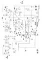
- a first embodiment of a closed loop ACT stage-based RF power amplifier linearization mechanism of the present inventionis diagrammatically illustrated as comprising an input terminal 10 to which an RF input signal RF IN (such as a multicarrier RF signal pictorially represented by a carrier frequency pair 12 ) is applied.
- the RF input terminal 10is coupled through a preamplifier 13 to a directional coupler (CPLR 1 ) 14 installed in a main signal flow path (designated by arrow MP) of a first, main RF amplifier 20 .
- CPLR 1directional coupler
- the main signal flow path MPcontains a first vector modulator 16 cascaded with a buffer amplifier 19 feeding the main RF amplifier 20 .
- the vector modulator unit 16may be implemented as a variable gain (attenuator) stage 17 series coupled with a variable phase shifting stage 18 .
- the variable gain stage 17 and phase shifting stage 18are controlled by control signals supplied over a control link 15 from a first carrier power control mechanism 116 executed within a digital signal processor (DSP) 100 .
- DSPdigital signal processor
- this first carrier power control mechanism 116monitors the output of a power detector 37 , which is coupled to a directional coupler 35 in the output path of a (pilot tone and distortion signal extracting) carrier cancellation (Wilkinson) combiner 30 of a carrier cancellation loop (loop 1 ).
- the carrier power control mechanism 116executes a standard error minimization (e.g., power or least mean squared minimization), and adjusts the vector modulator 16 input to the RF amplifier 20 , so that its contribution at the first input 31 of the carrier cancellation combiner 30 is the same amplitude and opposite phase as that of the RF carrier at the second input of the combiner 30 .
- the directional coupler 22 in the input path MP to main RF power amplifier 20is coupled to one output of a (Wilkinson) splitter 23 , which is coupled to receive a first, relatively low level, out-of-band pilot tone generated by a pilot tone generator 24 .
- This low level pilot toneis injected into the signal transport paths of each of the RF power amplifier 20 and a matched companion RF power amplifier 80 , and is used to track and cancel intermodulation distortion products produced by each amplifier.
- the vector modulator 25is used to adjust the amplitude and phase of pilot energy incident upon the RF power amplifier 80 , so that when vector modulator 50 is adjusted for optimum distortion cancellation at an output 93 of an output combiner 90 , the pilot energy is simultaneously nulled at output 93 as well.
- each amplifier outputwill contain a pilot tone component in addition to the desired RF signal and undesired IMDs. Since neither IMDs nor the pilot tone are part of the desired modulated carrier signal being amplified, they constitute unwanted distortion.
- the use of the pilot tone as a ‘pseudo noise’ signalallows the pilot to be treated as representative of whatever noise or distortion is produced by the amplifier pair. Therefore, by minimizing the contribution of the pilot tone to the composite output signal produced by the amplifier pair, IMDs are also minimized.
- the distortion minimization scheme of the inventioncontrols vector modulators for signal paths feeding the matched amplifier 80 by a pair of control loops, one monitoring pilot energy at the output of the composite ACT amplifier, and the other acting to equalize the desired carrier power at the outputs of the RF power amplifiers 20 and 80 , so that the two injected pilot tones (and therefore any intermodulation distortion products) cancel, while the desired RF carrier components constructively sum in the composite output of RF amplifiers 20 / 80 .
- a second output of splitter 23is applied to an amplitude/phase adjustor 25 , which sets the amplitude of the pilot tone and adjusts its phase, for application via a directional coupler 65 to the input signal path to RF amplifier 80 .
- the amplitude adjustmentis set such that the pilot signal produced at the output of amplifier 80 and applied to an input 92 of an output combiner 90 , shown configured as a four port combiner hybrid, will have exactly the same amplitude as the pilot signal produced at the output of amplifier 20 and applied to input 91 of output combiner 90 .
- the combiner's output port 93is monitored via a directional coupler 95 feeding an input port 103 of a pilot tone receiver, which is coupled to an energy minimization mechanism 110 in the DSP 100 .
- the pilot energy minimization mechanismcontrols the vector modulator 50 , so as to minimize (drive to zero) any pilot tone energy at the output combiner's output port 93 .
- a portion of the amplified output signal from the main path RF power amplifier 20is extracted via a further directional coupler 26 and coupled through an (output-scaling) attenuator pad 28 to input port 31 of the carrier cancellation combiner 30 .
- the second input port 32 of combiner 30is coupled to a first output 42 of a (Wilkinson) splitter 40 .
- Wilkinson splitter 40has its input 41 coupled through a delay line 34 in a signal flow path from directional coupler 14 . The delay imparted by the delay line 34 corresponds to the delay in the main signal path MP through the power amplifier 20 , thereby providing time alignment between the signals applied to carrier cancellation combiner 30 .
- the carrier components at inputs 31 and 32 of the carrier cancellation combiner 30are adjusted by the vector modulator to be of equal carrier amplitude and anti-phase, so that carrier cancellation occurs at output 33 .
- the carrier cancellation combiner 30provides an output (absent carrier energy) representative of an estimate of the residual distortion produced by the main power amplifier 20 (which includes the ‘pseudo distortion’ pilot tone produced by the pilot tone generator 24 and injected by directional coupler 22 .
- Carrier cancellation combiner 30has its output 33 coupled through a directional coupler 35 to the vector modulator 50 installed in a distortion energy transport path feeding a first input 61 of a distortion and carrier energy combiner 60 .
- the output of the directional coupler 35is detected by power detector 37 and represents the residual carrier energy left over after carrier cancellation in combiner 30 .
- the carrier power control mechanism 116minimizes detected carrier energy, by adjusting the vector modulator 16 input to the RF amplifier 20 , so that its contribution at the first input 31 of the carrier cancellation combiner 30 is the same as that of the RF carrier at the second input of the combiner 30 . This leaves only the pilot tone injected at the input of RF amplifier 20 and amplifier distortion energy at the carrier cancellation combiner output 33 .
- Wilkinson splitter 40has a second output 43 coupled to a variable gain stage 71 and variable phase shifter 73 of a vector modulator 70 installed in an input path to a second input 62 of the pilot/distortion and carrier energy combiner 60 .
- Vector modulator 70is operative to control the RF carrier energy therethrough so as to ensure that the RF carrier energy output from amplifier 80 is the same as that delivered by RF amplifier 20 .
- the residual power at port 94 of output combiner 90is monitored by power detector 97 which is coupled to input port 102 of DSP 100 .
- the output of power detector 97is applied to a second carrier power minimization-based control mechanism 117 within the DSP 100 .
- This second carrier power control mechanismcontrols the vector modulator 70 , so as to minimize (drive to zero) any carrier leakage energy at the output combiner's terminated port 94 , and thereby maximizing the carrier power delivered at port 93 of the output combiner 90 .
- the output 63 of the distortion and carrier energy combiner 60is coupled through a buffer amplifier 64 and antiphase pilot tone-injecting directional coupler 65 to RF amplifier 80 .
- the input to the RF amplifier 80includes three components.
- a firstis RF carrier energy extracted from the RF input 10 via splitter 40 and adjusted by the vector modulator 70 to match the RF carrier energy applied to the companion RF amplifier 20 .
- a secondcontains two distortion energy components—antiphase pilot tone and IMDs—which, when amplified by the RF amplifier 80 , will exactly oppositely match the pilot and IMD components produced at the output of RF amplifier 20 .
- the output combiner 90 of the multi vector modulator controlling, closed loop architecture of FIG. 2produces a summation of the signals applied to its inputs 91 and 92 , so that what is produced at output port 93 is a composite RF signal, in which the desired amplified RF carrier signals outputs produced by the two RF amplifiers 20 and 80 sum or constructively combine, and unwanted distortion products (including the injected pilot tones) destructively combine, or cancel.
- FIG. 3diagrammatically illustrates a second embodiment of the invention, having feed forward loops shown in broken lines 300 , that are ‘wrapped around’ the closed loop ACT-based RF power amplifier linearization architecture of FIG. 2, described above, and shown in broken lines as ACT RF amplifier linearization stage 200 .
- the addition of the feed forward loops 300enables the integrated amplifier architecture (containing the RF amplifier linearization stage 200 and the feed forward loops 300 ) to deliver extremely high linearity, including the ability to routinely achieve carrier-to distortion ratios as high as 85 dB. Efficiency is significantly better than that which is typically seen in competitive dual loop feed forward power amplifiers.
- the ‘wrapped around’ feed forward loops 300 of the embodiment of FIG. 3include a buffer amplifier 313 and a further directional coupler 314 coupled between the RF input terminal 10 and the main signal flow path of the ACT RF amplifier linearization stage 200 .
- a first main path through the directional coupler 314is coupled to a vector modulator 316 , having a processor-controlled variable gain (attenuator) stage 317 and a processor-controlled variable phase shifting stage 318 cascaded with variable gain stage 317 .
- the output port 93 of the output combiner 90 of the amplifier linearization stage 200is coupled through a circulator 302 to a directional coupler 328 , used to extract a portion of the amplified output signal from the output combiner's output port 93 .
- This extracted output signalis coupled through an (output-scaling) attenuator pad 329 to a first input 331 of a carrier cancellation (Wilkinson) combiner 330 within a further carrier cancellation loop (loop 3 ).
- a second input 332 of the carrier cancellation combiner 330is coupled to a first delay line 336 installed in a second signal flow path from the directional coupler 314 .
- the delay imparted by the delay line 336corresponds to the delay in the signal path through the amplifier stage 200 , and serves to time-align the two signals applied to the carrier cancellation combiner 330 .
- the carrier cancellation combiner 330provides a ‘further refined’ estimate of the residual distortion produced by the ACT RF amplifier linearization stage 200 .
- Carrier rejection within the feed forward stage 300is optimized by carrier power minimization mechanism 136 within DSP 100 , which is coupled via a DSP input port 104 to a power detector 337 , coupled to a directional coupler 338 at the output of the carrier cancellation combiner 330 .
- the carrier power minimization mechanism 136executes a detected power minimization algorithm, and outputs signals for controlling the attenuator 317 and the phase shifter 318 of the vector modulator 316 in the RF input path of the amplifier stage 200 , so as to set the input RF carrier energy at a value that will cause the RF carrier power in the composite output signal at combiner output port 93 , when scaled by attenuator 329 , to cancel the RF input energy applied to the second input 332 of carrier cancellation combiner 330 .
- the distortion energy-representative output 333 of carrier cancellation combiner 330is coupled to a vector modulator 346 of a feed-forward distortion cancellation loop (loop 4 ).
- vector modulator 346contains a processor-controlled variable gain stage 347 cascaded with a processor-controlled variable phase shifting stage 348 .
- the output of the vector modulator 346is coupled through a buffer amplifier 351 and a directional coupler 353 to a feed-forward error amplifier 360 of loop 4 .
- the feed-forward error amplifier 360amplifies the gain and phased adjusted residual power amplifier distortion derived from the carrier cancellation combiner 330 of loop 3 and injects the error signal to the amplifier's output signal path via directional coupler 371 .
- the directional coupler 666 at the output of the composite ACT/Feedforward amplifiercouples a portion of the distortion signal to an input port 105 of a further pilot tone receiver 667 , which drives a further pilot energy minimization mechanism 668 within DSP 100 .
- This auxiliary pilot tone minimization mechanism 668adjusts the parameters of the vector modulator 346 based upon detected pilot tone distortion energy, to produce auxiliary distortion signal products that are equal in amplitude and opposite in phase from the original amplifier distortion of ACT main RF amplifier stage 200 . These distortion products provide further cancellation of any remaining distortion generated by the main RF amplifier stage 200 when the feed forward error path is reinjected into the output of the output combiner 90 at directional coupler 371 .
- Directional coupler 371is installed between a delay line 373 in the output path of the output combiner 90 and the output directional coupler 95 . Similar to the use of delay line 336 , the delay imparted by the delay line 373 equals the signal propagation delay through in error amplifier path and serves to ensure there is adequate phase matching at the feed forward directional coupler 371 over the operating frequency range.
- the output of directional coupler 371corresponds to a recombination of the amplified feed-forward signal anti-phase with a delayed version of the output signal from the main path amplifier stage 200 , and achieves very high distortion suppression so that the linearity of the amplifier is significantly enhanced.
- Directional coupler 353samples distortion and residual pilot energy due to imperfect adjustment of the ACT amplifier stage 200 . Pilot energy at the output of direction coupler 353 is sensed by pilot receiver 114 and used to control ACT vector modulator 50 via a power minimization loop 110 to minimize distortion at the output of the ACT amplifier stage 200 .
- the output direction coupler 95samples desired carrier, pilot and distortion energy at the output of the ACT power amplifier.
- the directional coupler 353samples the same energy, with the carrier power substantially eliminated by the carrier cancellation process of loop 3 of the feedforward process.
- the pilot signal to carrier ratio at the coupled port of directional coupler 353is enhanced over that of the coupled port of the directional coupler 95 of the embodiment of FIG. 2 .
- pilot energy at the coupled port of directional coupler 353is used to control the ACT vector modulator 50 via the pilot receiver 114 and energy minimization mechanism 110 .
- the power minimization and performance monitor controllers and associated pilot generator and pilot receiver circuits of the ACT RF amplifier linearization stage 200maintain distortion cancellation in the pre-distortion loop, while the feed forward loop of the feed-forward stage 300 results in a simplification in circuit implementation that reduces amplifier size, complexity and cost.
- the potential amplifier output signal and distortion energy inequality problem of an open loop ACT-based RF power amplifier linearization architectureis substantially minimized, by injecting a pilot tone as a ‘pseudo distortion’ signal and using a set of power minimization loops that are closed around the RF amplifier pair.
- the power minimizing control loopscontrol a set of vector modulators such that both the injected pilot tone and intermodulation distortion products are canceled, while RF carrier components constructively sum in the composite output of the amplifiers.
- Both signal summation adjustment and distortion cancellation adjustmentmay be independently maintained to provide more than 20 dB of distortion reduction over a wide range of supply voltage, temperature and different input signal characteristics.
- the amplitude of the distortion productsmay be decreased by up to another 35 dB.
- the addition of the feed-forward looppermits an overall signal-to-distortion ratio as high as 85 dBc to be achieved. Because the closed loop ACT pre-distortion architecture is more efficient than a equivalent single loop feed forward power amplifier, the overall system is several percent more efficient than a dual loop feed forward design with similar performance.
Landscapes
- Physics & Mathematics (AREA)
- Nonlinear Science (AREA)
- Engineering & Computer Science (AREA)
- Power Engineering (AREA)
- Amplifiers (AREA)
Abstract
Description
Claims (20)
Priority Applications (4)
| Application Number | Priority Date | Filing Date | Title |
|---|---|---|---|
| US10/034,016US6452446B1 (en) | 2000-12-29 | 2001-12-20 | Closed loop active cancellation technique (ACT)-based RF power amplifier linearization architecture |
| DE60137643TDE60137643D1 (en) | 2000-12-29 | 2001-12-21 | LINEARIZATION ARCHITECTURE FOR A HF POWER AMPLIFIER BASED ON CLOSED LOOP ACTIVE CLEARING TECHNOLOGY (ACT) |
| EP01991348AEP1346472B1 (en) | 2000-12-29 | 2001-12-21 | Closed loop active cancellation technique (act)-based rf power amplifier linearization architecture |
| PCT/US2001/049237WO2002054590A1 (en) | 2000-12-29 | 2001-12-21 | Closed loop active cancellation technique (act)-based rf power amplifier linearization architecture |
Applications Claiming Priority (2)
| Application Number | Priority Date | Filing Date | Title |
|---|---|---|---|
| US25901200P | 2000-12-29 | 2000-12-29 | |
| US10/034,016US6452446B1 (en) | 2000-12-29 | 2001-12-20 | Closed loop active cancellation technique (ACT)-based RF power amplifier linearization architecture |
Publications (2)
| Publication Number | Publication Date |
|---|---|
| US20020084845A1 US20020084845A1 (en) | 2002-07-04 |
| US6452446B1true US6452446B1 (en) | 2002-09-17 |
Family
ID=26710445
Family Applications (1)
| Application Number | Title | Priority Date | Filing Date |
|---|---|---|---|
| US10/034,016Expired - LifetimeUS6452446B1 (en) | 2000-12-29 | 2001-12-20 | Closed loop active cancellation technique (ACT)-based RF power amplifier linearization architecture |
Country Status (4)
| Country | Link |
|---|---|
| US (1) | US6452446B1 (en) |
| EP (1) | EP1346472B1 (en) |
| DE (1) | DE60137643D1 (en) |
| WO (1) | WO2002054590A1 (en) |
Cited By (31)
| Publication number | Priority date | Publication date | Assignee | Title |
|---|---|---|---|---|
| US20040021517A1 (en)* | 2002-08-05 | 2004-02-05 | Spectrian Corporation | Power minimization, correlation-based closed loop for controlling predistorter and vector modulator feeding RF power amplifier |
| US20040119535A1 (en)* | 2002-12-18 | 2004-06-24 | Hunton Matthew J. | Feed forward amplifier system using penalties and floors for optimal control |
| US20040152433A1 (en)* | 2003-01-23 | 2004-08-05 | Braithwaite Richard Neil | Feed forward amplifier system employing self-generating alignment lists and adaptive controller |
| US20040204100A1 (en)* | 2003-04-10 | 2004-10-14 | Braithwaite Richard Neil | Multi-transmitter communication system employing anti-phase pilot signals |
| US20040235437A1 (en)* | 2003-03-12 | 2004-11-25 | Gels Robert G. | Closed loop power control of non-constant envelope waveforms using sample/hold |
| US20040251961A1 (en)* | 2003-05-07 | 2004-12-16 | Braithwaite Richard Neil | Feed forward amplifier employing positive feedback pilot generation |
| US20060033607A1 (en)* | 2004-04-30 | 2006-02-16 | The Board Of Trustees Of The Leland Stanford Junior University | System and method for sensitivity optimization of RF receiver using adaptive nulling |
| US7002407B2 (en) | 2002-12-18 | 2006-02-21 | Powerwave Technologies, Inc. | Delay mismatched feed forward amplifier system using penalties and floors for control |
| US7184723B2 (en) | 2004-10-22 | 2007-02-27 | Parkervision, Inc. | Systems and methods for vector power amplification |
| US20070222513A1 (en)* | 2006-03-09 | 2007-09-27 | Kossor Michael G | Apparatus and method for processing of amplifier linearization signals |
| US7355470B2 (en) | 2006-04-24 | 2008-04-08 | Parkervision, Inc. | Systems and methods of RF power transmission, modulation, and amplification, including embodiments for amplifier class transitioning |
| US7620129B2 (en) | 2007-01-16 | 2009-11-17 | Parkervision, Inc. | RF power transmission, modulation, and amplification, including embodiments for generating vector modulation control signals |
| US20100033246A1 (en)* | 2008-08-11 | 2010-02-11 | Qualcomm Incorporated | Adaptive digital predistortion of complex modulated waveform using peak and rms voltage feedback from the output of a power amplifier |
| US20100237942A1 (en)* | 2009-03-19 | 2010-09-23 | Qualcomm Incorporated | Common-gate common-source amplifier |
| US7885682B2 (en) | 2006-04-24 | 2011-02-08 | Parkervision, Inc. | Systems and methods of RF power transmission, modulation, and amplification, including architectural embodiments of same |
| US7911272B2 (en) | 2007-06-19 | 2011-03-22 | Parkervision, Inc. | Systems and methods of RF power transmission, modulation, and amplification, including blended control embodiments |
| US8013675B2 (en) | 2007-06-19 | 2011-09-06 | Parkervision, Inc. | Combiner-less multiple input single output (MISO) amplification with blended control |
| US8031804B2 (en) | 2006-04-24 | 2011-10-04 | Parkervision, Inc. | Systems and methods of RF tower transmission, modulation, and amplification, including embodiments for compensating for waveform distortion |
| US20120001686A1 (en)* | 2010-06-30 | 2012-01-05 | Icom Incorporated | High frequency circuit |
| US20120154033A1 (en)* | 2010-12-17 | 2012-06-21 | Fujitsu Limited | Amplifying apparatus and distortion compensation method |
| US8315336B2 (en) | 2007-05-18 | 2012-11-20 | Parkervision, Inc. | Systems and methods of RF power transmission, modulation, and amplification, including a switching stage embodiment |
| US8334722B2 (en) | 2007-06-28 | 2012-12-18 | Parkervision, Inc. | Systems and methods of RF power transmission, modulation and amplification |
| US8755454B2 (en) | 2011-06-02 | 2014-06-17 | Parkervision, Inc. | Antenna control |
| US9106316B2 (en) | 2005-10-24 | 2015-08-11 | Parkervision, Inc. | Systems and methods of RF power transmission, modulation, and amplification |
| US9214968B2 (en) | 2013-07-24 | 2015-12-15 | Nokia Technologies Oy | Apparatus and methods for providing a power amplifier with interference cancellation |
| US9479214B2 (en) | 2013-11-25 | 2016-10-25 | Raytheon Company | Wideband active radio frequency interference cancellation system |
| US9553712B2 (en) | 2013-11-25 | 2017-01-24 | Raytheon Company | Feed-forward canceller |
| US9608677B2 (en) | 2005-10-24 | 2017-03-28 | Parker Vision, Inc | Systems and methods of RF power transmission, modulation, and amplification |
| US9837966B1 (en)* | 2016-08-26 | 2017-12-05 | Nxp Usa, Inc. | Series-type Doherty amplifier |
| US10278131B2 (en) | 2013-09-17 | 2019-04-30 | Parkervision, Inc. | Method, apparatus and system for rendering an information bearing function of time |
| WO2022229682A1 (en)* | 2021-04-30 | 2022-11-03 | Telefonaktiebolaget Lm Ericsson (Publ) | Magnitude and phase adjustment method for high output power rf power amplifier combining |
Families Citing this family (12)
| Publication number | Priority date | Publication date | Assignee | Title |
|---|---|---|---|---|
| US7064608B2 (en) | 2002-11-26 | 2006-06-20 | Scriptl, Llc | Feed-forward-back suppressed noise circuits |
| GB2396497B (en)* | 2002-12-20 | 2005-08-03 | Motorola Inc | Wireless communication unit and transmitter circuit therefor |
| JP3910167B2 (en)* | 2003-09-25 | 2007-04-25 | 松下電器産業株式会社 | Amplifier circuit |
| EP2145386B1 (en)* | 2007-05-04 | 2013-11-20 | Astrium Limited | Multiport amplifiers in communications satellites |
| CN101393959B (en)* | 2008-11-07 | 2012-04-11 | 中国科学院上海硅酸盐研究所 | Cage type compound |
| US8626090B2 (en) | 2010-03-23 | 2014-01-07 | Telefonaktiebolaget Lm Ericsson (Publ) | Circuit and method for interference reduction |
| US8514007B1 (en) | 2012-01-27 | 2013-08-20 | Freescale Semiconductor, Inc. | Adjustable power splitter and corresponding methods and apparatus |
| US10018707B2 (en)* | 2014-05-02 | 2018-07-10 | The United States Of America As Represented By The Secretary Of The Army | Automated cancellation of harmonics using feed forward filter reflection for radar transmitter linearization |
| US9774299B2 (en)* | 2014-09-29 | 2017-09-26 | Nxp Usa, Inc. | Modifiable signal adjustment devices for power amplifiers and corresponding methods and apparatus |
| WO2016187300A1 (en)* | 2015-05-18 | 2016-11-24 | William Marsh Rice University | Electron paramagnetic resonance (epr) systems with active cancellation |
| CN107947755B (en)* | 2016-10-11 | 2021-06-29 | 康普技术有限责任公司 | energy absorption circuit |
| CN106603094B (en)* | 2016-11-22 | 2019-11-08 | Tcl移动通信科技(宁波)有限公司 | A kind of method and circuit of radio-frequency transmissions |
Citations (5)
| Publication number | Priority date | Publication date | Assignee | Title |
|---|---|---|---|---|
| US5386198A (en)* | 1993-01-28 | 1995-01-31 | Telefonaktiebolaget L M Ericsson | Linear amplifier control |
| US6066984A (en)* | 1998-03-16 | 2000-05-23 | Hitachi Denshi Kabushiki Kaisha | Amplifier and amplifying method for amplifying a plurality of signals having different bands simultaneously |
| US6104241A (en) | 1998-11-18 | 2000-08-15 | Spectrian | High efficiency feed-forward RF power amplifier with predistoration enchancement |
| US6111462A (en) | 1998-11-18 | 2000-08-29 | Mucenieks; Lance T. | RF power amplifier linearization using parallel RF power amplifiers having intermod-complementing predistortion paths |
| US6208207B1 (en)* | 1999-05-05 | 2001-03-27 | Simon Fraser University | Adaptive linearizer for RF power amplifiers |
Family Cites Families (1)
| Publication number | Priority date | Publication date | Assignee | Title |
|---|---|---|---|---|
| US5621354A (en)* | 1995-10-17 | 1997-04-15 | Motorola, Inc. | Apparatus and method for performing error corrected amplification in a radio frequency system |
- 2001
- 2001-12-20USUS10/034,016patent/US6452446B1/ennot_activeExpired - Lifetime
- 2001-12-21DEDE60137643Tpatent/DE60137643D1/ennot_activeExpired - Fee Related
- 2001-12-21WOPCT/US2001/049237patent/WO2002054590A1/ennot_activeApplication Discontinuation
- 2001-12-21EPEP01991348Apatent/EP1346472B1/ennot_activeExpired - Lifetime
Patent Citations (5)
| Publication number | Priority date | Publication date | Assignee | Title |
|---|---|---|---|---|
| US5386198A (en)* | 1993-01-28 | 1995-01-31 | Telefonaktiebolaget L M Ericsson | Linear amplifier control |
| US6066984A (en)* | 1998-03-16 | 2000-05-23 | Hitachi Denshi Kabushiki Kaisha | Amplifier and amplifying method for amplifying a plurality of signals having different bands simultaneously |
| US6104241A (en) | 1998-11-18 | 2000-08-15 | Spectrian | High efficiency feed-forward RF power amplifier with predistoration enchancement |
| US6111462A (en) | 1998-11-18 | 2000-08-29 | Mucenieks; Lance T. | RF power amplifier linearization using parallel RF power amplifiers having intermod-complementing predistortion paths |
| US6208207B1 (en)* | 1999-05-05 | 2001-03-27 | Simon Fraser University | Adaptive linearizer for RF power amplifiers |
Cited By (93)
| Publication number | Priority date | Publication date | Assignee | Title |
|---|---|---|---|---|
| US20040021517A1 (en)* | 2002-08-05 | 2004-02-05 | Spectrian Corporation | Power minimization, correlation-based closed loop for controlling predistorter and vector modulator feeding RF power amplifier |
| US20040119535A1 (en)* | 2002-12-18 | 2004-06-24 | Hunton Matthew J. | Feed forward amplifier system using penalties and floors for optimal control |
| WO2004062091A1 (en)* | 2002-12-18 | 2004-07-22 | Powerwave Technologies, Inc. | Feed forward amplifier system using penalties and floors for optimal control |
| US6998916B2 (en) | 2002-12-18 | 2006-02-14 | Powerwave Technologies, Inc. | Feed forward amplifier system using penalties and floors for optimal control |
| US7002407B2 (en) | 2002-12-18 | 2006-02-21 | Powerwave Technologies, Inc. | Delay mismatched feed forward amplifier system using penalties and floors for control |
| US20040152433A1 (en)* | 2003-01-23 | 2004-08-05 | Braithwaite Richard Neil | Feed forward amplifier system employing self-generating alignment lists and adaptive controller |
| US6985706B2 (en) | 2003-01-23 | 2006-01-10 | Powerwave Technologies, Inc. | Feed forward amplifier system employing self-generating alignment lists and adaptive controller |
| US20040235437A1 (en)* | 2003-03-12 | 2004-11-25 | Gels Robert G. | Closed loop power control of non-constant envelope waveforms using sample/hold |
| US7353006B2 (en)* | 2003-03-12 | 2008-04-01 | Analog Devices, Inc. | Closed loop power control of non-constant envelope waveforms using sample/hold |
| US7110739B2 (en) | 2003-04-10 | 2006-09-19 | Powerwave Technologies, Inc. | Multi-transmitter communication system employing anti-phase pilot signals |
| US20040204100A1 (en)* | 2003-04-10 | 2004-10-14 | Braithwaite Richard Neil | Multi-transmitter communication system employing anti-phase pilot signals |
| US20040251961A1 (en)* | 2003-05-07 | 2004-12-16 | Braithwaite Richard Neil | Feed forward amplifier employing positive feedback pilot generation |
| US7123086B2 (en) | 2003-05-07 | 2006-10-17 | Powerwave Technologies, Inc. | Feed forward amplifier employing positive feedback pilot generation |
| US20060033607A1 (en)* | 2004-04-30 | 2006-02-16 | The Board Of Trustees Of The Leland Stanford Junior University | System and method for sensitivity optimization of RF receiver using adaptive nulling |
| US7369811B2 (en)* | 2004-04-30 | 2008-05-06 | Wj Communications, Inc. | System and method for sensitivity optimization of RF receiver using adaptive nulling |
| US7647030B2 (en) | 2004-10-22 | 2010-01-12 | Parkervision, Inc. | Multiple input single output (MISO) amplifier with circuit branch output tracking |
| US9197163B2 (en) | 2004-10-22 | 2015-11-24 | Parkvision, Inc. | Systems, and methods of RF power transmission, modulation, and amplification, including embodiments for output stage protection |
| US9768733B2 (en) | 2004-10-22 | 2017-09-19 | Parker Vision, Inc. | Multiple input single output device with vector signal and bias signal inputs |
| US8280321B2 (en) | 2004-10-22 | 2012-10-02 | Parkervision, Inc. | Systems and methods of RF power transmission, modulation, and amplification, including Cartesian-Polar-Cartesian-Polar (CPCP) embodiments |
| US8233858B2 (en) | 2004-10-22 | 2012-07-31 | Parkervision, Inc. | RF power transmission, modulation, and amplification embodiments, including control circuitry for controlling power amplifier output stages |
| US8406711B2 (en) | 2004-10-22 | 2013-03-26 | Parkervision, Inc. | Systems and methods of RF power transmission, modulation, and amplification, including a Cartesian-Polar-Cartesian-Polar (CPCP) embodiment |
| US7421036B2 (en) | 2004-10-22 | 2008-09-02 | Parkervision, Inc. | Systems and methods of RF power transmission, modulation, and amplification, including transfer function embodiments |
| US8428527B2 (en) | 2004-10-22 | 2013-04-23 | Parkervision, Inc. | RF power transmission, modulation, and amplification, including direct cartesian 2-branch embodiments |
| US7466760B2 (en) | 2004-10-22 | 2008-12-16 | Parkervision, Inc. | Systems and methods of RF power transmission, modulation, and amplification, including transfer function embodiments |
| US7526261B2 (en) | 2004-10-22 | 2009-04-28 | Parkervision, Inc. | RF power transmission, modulation, and amplification, including cartesian 4-branch embodiments |
| US7327803B2 (en) | 2004-10-22 | 2008-02-05 | Parkervision, Inc. | Systems and methods for vector power amplification |
| US7639072B2 (en) | 2004-10-22 | 2009-12-29 | Parkervision, Inc. | Controlling a power amplifier to transition among amplifier operational classes according to at least an output signal waveform trajectory |
| US8351870B2 (en) | 2004-10-22 | 2013-01-08 | Parkervision, Inc. | Systems and methods of RF power transmission, modulation, and amplification, including cartesian 4-branch embodiments |
| US9197164B2 (en) | 2004-10-22 | 2015-11-24 | Parkervision, Inc. | RF power transmission, modulation, and amplification, including direct cartesian 2-branch embodiments |
| US7672650B2 (en) | 2004-10-22 | 2010-03-02 | Parkervision, Inc. | Systems and methods of RF power transmission, modulation, and amplification, including multiple input single output (MISO) amplifier embodiments comprising harmonic control circuitry |
| US8577313B2 (en) | 2004-10-22 | 2013-11-05 | Parkervision, Inc. | Systems and methods of RF power transmission, modulation, and amplification, including output stage protection circuitry |
| US9166528B2 (en) | 2004-10-22 | 2015-10-20 | Parkervision, Inc. | RF power transmission, modulation, and amplification embodiments |
| US7835709B2 (en) | 2004-10-22 | 2010-11-16 | Parkervision, Inc. | RF power transmission, modulation, and amplification using multiple input single output (MISO) amplifiers to process phase angle and magnitude information |
| US7844235B2 (en) | 2004-10-22 | 2010-11-30 | Parkervision, Inc. | RF power transmission, modulation, and amplification, including harmonic control embodiments |
| US8433264B2 (en) | 2004-10-22 | 2013-04-30 | Parkervision, Inc. | Multiple input single output (MISO) amplifier having multiple transistors whose output voltages substantially equal the amplifier output voltage |
| US9143088B2 (en) | 2004-10-22 | 2015-09-22 | Parkervision, Inc. | Control modules |
| US7184723B2 (en) | 2004-10-22 | 2007-02-27 | Parkervision, Inc. | Systems and methods for vector power amplification |
| US8447248B2 (en) | 2004-10-22 | 2013-05-21 | Parkervision, Inc. | RF power transmission, modulation, and amplification, including power control of multiple input single output (MISO) amplifiers |
| US7932776B2 (en) | 2004-10-22 | 2011-04-26 | Parkervision, Inc. | RF power transmission, modulation, and amplification embodiments |
| US8913974B2 (en) | 2004-10-22 | 2014-12-16 | Parkervision, Inc. | RF power transmission, modulation, and amplification, including direct cartesian 2-branch embodiments |
| US7945224B2 (en) | 2004-10-22 | 2011-05-17 | Parkervision, Inc. | Systems and methods of RF power transmission, modulation, and amplification, including waveform distortion compensation embodiments |
| US8781418B2 (en) | 2004-10-22 | 2014-07-15 | Parkervision, Inc. | Power amplification based on phase angle controlled reference signal and amplitude control signal |
| US8639196B2 (en) | 2004-10-22 | 2014-01-28 | Parkervision, Inc. | Control modules |
| US8626093B2 (en) | 2004-10-22 | 2014-01-07 | Parkervision, Inc. | RF power transmission, modulation, and amplification embodiments |
| US9419692B2 (en) | 2005-10-24 | 2016-08-16 | Parkervision, Inc. | Antenna control |
| US9094085B2 (en) | 2005-10-24 | 2015-07-28 | Parkervision, Inc. | Control of MISO node |
| US9106316B2 (en) | 2005-10-24 | 2015-08-11 | Parkervision, Inc. | Systems and methods of RF power transmission, modulation, and amplification |
| US9608677B2 (en) | 2005-10-24 | 2017-03-28 | Parker Vision, Inc | Systems and methods of RF power transmission, modulation, and amplification |
| US9614484B2 (en) | 2005-10-24 | 2017-04-04 | Parkervision, Inc. | Systems and methods of RF power transmission, modulation, and amplification, including control functions to transition an output of a MISO device |
| US9705540B2 (en) | 2005-10-24 | 2017-07-11 | Parker Vision, Inc. | Control of MISO node |
| US7856105B2 (en) | 2006-03-09 | 2010-12-21 | Andrew Llc | Apparatus and method for processing of amplifier linearization signals |
| US20070222513A1 (en)* | 2006-03-09 | 2007-09-27 | Kossor Michael G | Apparatus and method for processing of amplifier linearization signals |
| US8050353B2 (en) | 2006-04-24 | 2011-11-01 | Parkervision, Inc. | Systems and methods of RF power transmission, modulation, and amplification, including embodiments for compensating for waveform distortion |
| US7949365B2 (en) | 2006-04-24 | 2011-05-24 | Parkervision, Inc. | Systems and methods of RF power transmission, modulation, and amplification, including architectural embodiments of same |
| US7355470B2 (en) | 2006-04-24 | 2008-04-08 | Parkervision, Inc. | Systems and methods of RF power transmission, modulation, and amplification, including embodiments for amplifier class transitioning |
| US7378902B2 (en) | 2006-04-24 | 2008-05-27 | Parkervision, Inc | Systems and methods of RF power transmission, modulation, and amplification, including embodiments for gain and phase control |
| US7414469B2 (en) | 2006-04-24 | 2008-08-19 | Parkervision, Inc. | Systems and methods of RF power transmission, modulation, and amplification, including embodiments for amplifier class transitioning |
| US7423477B2 (en) | 2006-04-24 | 2008-09-09 | Parkervision, Inc. | Systems and methods of RF power transmission, modulation, and amplification, including embodiments for amplifier class transitioning |
| US7750733B2 (en) | 2006-04-24 | 2010-07-06 | Parkervision, Inc. | Systems and methods of RF power transmission, modulation, and amplification, including embodiments for extending RF transmission bandwidth |
| US7885682B2 (en) | 2006-04-24 | 2011-02-08 | Parkervision, Inc. | Systems and methods of RF power transmission, modulation, and amplification, including architectural embodiments of same |
| US8059749B2 (en) | 2006-04-24 | 2011-11-15 | Parkervision, Inc. | Systems and methods of RF power transmission, modulation, and amplification, including embodiments for compensating for waveform distortion |
| US8036306B2 (en) | 2006-04-24 | 2011-10-11 | Parkervision, Inc. | Systems and methods of RF power transmission, modulation and amplification, including embodiments for compensating for waveform distortion |
| US9106500B2 (en) | 2006-04-24 | 2015-08-11 | Parkervision, Inc. | Systems and methods of RF power transmission, modulation, and amplification, including embodiments for error correction |
| US7929989B2 (en) | 2006-04-24 | 2011-04-19 | Parkervision, Inc. | Systems and methods of RF power transmission, modulation, and amplification, including architectural embodiments of same |
| US7937106B2 (en) | 2006-04-24 | 2011-05-03 | ParkerVision, Inc, | Systems and methods of RF power transmission, modulation, and amplification, including architectural embodiments of same |
| US8031804B2 (en) | 2006-04-24 | 2011-10-04 | Parkervision, Inc. | Systems and methods of RF tower transmission, modulation, and amplification, including embodiments for compensating for waveform distortion |
| US8026764B2 (en) | 2006-04-24 | 2011-09-27 | Parkervision, Inc. | Generation and amplification of substantially constant envelope signals, including switching an output among a plurality of nodes |
| US8913691B2 (en) | 2006-08-24 | 2014-12-16 | Parkervision, Inc. | Controlling output power of multiple-input single-output (MISO) device |
| US7620129B2 (en) | 2007-01-16 | 2009-11-17 | Parkervision, Inc. | RF power transmission, modulation, and amplification, including embodiments for generating vector modulation control signals |
| US8548093B2 (en) | 2007-05-18 | 2013-10-01 | Parkervision, Inc. | Power amplification based on frequency control signal |
| US8315336B2 (en) | 2007-05-18 | 2012-11-20 | Parkervision, Inc. | Systems and methods of RF power transmission, modulation, and amplification, including a switching stage embodiment |
| US8410849B2 (en) | 2007-06-19 | 2013-04-02 | Parkervision, Inc. | Systems and methods of RF power transmission, modulation, and amplification, including blended control embodiments |
| US8766717B2 (en) | 2007-06-19 | 2014-07-01 | Parkervision, Inc. | Systems and methods of RF power transmission, modulation, and amplification, including varying weights of control signals |
| US8013675B2 (en) | 2007-06-19 | 2011-09-06 | Parkervision, Inc. | Combiner-less multiple input single output (MISO) amplification with blended control |
| US8502600B2 (en) | 2007-06-19 | 2013-08-06 | Parkervision, Inc. | Combiner-less multiple input single output (MISO) amplification with blended control |
| US8461924B2 (en) | 2007-06-19 | 2013-06-11 | Parkervision, Inc. | Systems and methods of RF power transmission, modulation, and amplification, including embodiments for controlling a transimpedance node |
| US7911272B2 (en) | 2007-06-19 | 2011-03-22 | Parkervision, Inc. | Systems and methods of RF power transmission, modulation, and amplification, including blended control embodiments |
| US8334722B2 (en) | 2007-06-28 | 2012-12-18 | Parkervision, Inc. | Systems and methods of RF power transmission, modulation and amplification |
| US8884694B2 (en) | 2007-06-28 | 2014-11-11 | Parkervision, Inc. | Systems and methods of RF power transmission, modulation, and amplification |
| US20100033246A1 (en)* | 2008-08-11 | 2010-02-11 | Qualcomm Incorporated | Adaptive digital predistortion of complex modulated waveform using peak and rms voltage feedback from the output of a power amplifier |
| US8384476B2 (en)* | 2008-08-11 | 2013-02-26 | Qualcomm, Incorporated | Adaptive digital predistortion of complex modulated waveform using peak and RMS voltage feedback from the output of a power amplifier |
| US20100237942A1 (en)* | 2009-03-19 | 2010-09-23 | Qualcomm Incorporated | Common-gate common-source amplifier |
| US8295796B2 (en)* | 2010-06-30 | 2012-10-23 | Icom Incorporated | High frequency circuit |
| US20120001686A1 (en)* | 2010-06-30 | 2012-01-05 | Icom Incorporated | High frequency circuit |
| US20120154033A1 (en)* | 2010-12-17 | 2012-06-21 | Fujitsu Limited | Amplifying apparatus and distortion compensation method |
| US8686791B2 (en)* | 2010-12-17 | 2014-04-01 | Fujitsu Limited | Amplifying apparatus and distortion compensation method |
| US8755454B2 (en) | 2011-06-02 | 2014-06-17 | Parkervision, Inc. | Antenna control |
| US9214968B2 (en) | 2013-07-24 | 2015-12-15 | Nokia Technologies Oy | Apparatus and methods for providing a power amplifier with interference cancellation |
| US10278131B2 (en) | 2013-09-17 | 2019-04-30 | Parkervision, Inc. | Method, apparatus and system for rendering an information bearing function of time |
| US9553712B2 (en) | 2013-11-25 | 2017-01-24 | Raytheon Company | Feed-forward canceller |
| US9479214B2 (en) | 2013-11-25 | 2016-10-25 | Raytheon Company | Wideband active radio frequency interference cancellation system |
| US9837966B1 (en)* | 2016-08-26 | 2017-12-05 | Nxp Usa, Inc. | Series-type Doherty amplifier |
| WO2022229682A1 (en)* | 2021-04-30 | 2022-11-03 | Telefonaktiebolaget Lm Ericsson (Publ) | Magnitude and phase adjustment method for high output power rf power amplifier combining |
Also Published As
| Publication number | Publication date |
|---|---|
| EP1346472A4 (en) | 2004-05-12 |
| EP1346472B1 (en) | 2009-02-11 |
| DE60137643D1 (en) | 2009-03-26 |
| WO2002054590A1 (en) | 2002-07-11 |
| EP1346472A1 (en) | 2003-09-24 |
| US20020084845A1 (en) | 2002-07-04 |
Similar Documents
| Publication | Publication Date | Title |
|---|---|---|
| US6452446B1 (en) | Closed loop active cancellation technique (ACT)-based RF power amplifier linearization architecture | |
| EP1293039B1 (en) | High linearity multicarrier rf amplifier | |
| US6104241A (en) | High efficiency feed-forward RF power amplifier with predistoration enchancement | |
| US6111462A (en) | RF power amplifier linearization using parallel RF power amplifiers having intermod-complementing predistortion paths | |
| JP3342018B2 (en) | RF amplifier having adaptive predistortion circuit | |
| KR100345620B1 (en) | Error extraction using autocalibrating rf correlator | |
| US20040021517A1 (en) | Power minimization, correlation-based closed loop for controlling predistorter and vector modulator feeding RF power amplifier | |
| US8064851B2 (en) | RF transmitter with bias-signal-induced distortion compensation and method therefor | |
| EP1042864B1 (en) | Method and apparatus for wideband predistortion linearization | |
| EP1158661B1 (en) | Feed-forward amplifier | |
| US6275106B1 (en) | Spectral distortion monitor for controlling pre-distortion and feed-forward linearization of rf power amplifier | |
| WO1998004034A9 (en) | Rf amplifier having adaptative predistortion circuit | |
| US5977826A (en) | Cascaded error correction in a feed forward amplifier | |
| US7301397B2 (en) | Enhanced efficiency feed forward power amplifier with delay mismatched error cancellation loop | |
| EP1066680B1 (en) | Predistorter | |
| US6400223B1 (en) | Double carrier cancellation in wide band multi-carrier feed forward linearized power amplifier | |
| KR100309720B1 (en) | Feed-forward linear power amplifier with amplifier for compensating delay | |
| WO2004040751A1 (en) | Amplifier assembly |
Legal Events
| Date | Code | Title | Description |
|---|---|---|---|
| AS | Assignment | Owner name:SPECTRIAN CORPORATION, CALIFORNIA Free format text:ASSIGNMENT OF ASSIGNORS INTEREST;ASSIGNORS:EISENBERG, JOHN;AVIS, STEVE;REEL/FRAME:012439/0991 Effective date:20011218 | |
| STCF | Information on status: patent grant | Free format text:PATENTED CASE | |
| AS | Assignment | Owner name:REMEC, INC., CALIFORNIA Free format text:ASSIGNMENT OF ASSIGNORS INTEREST;ASSIGNOR:SPECTRIAN CORPORATION;REEL/FRAME:013949/0866 Effective date:20030324 | |
| AS | Assignment | Owner name:GSLE SUBCO L.L.C., NORTH CAROLINA Free format text:MERGER;ASSIGNOR:SPX DEVELOPMENT CORPORATION;REEL/FRAME:016182/0067 Effective date:20041231 | |
| FPAY | Fee payment | Year of fee payment:4 | |
| AS | Assignment | Owner name:POWERWAVE TECHNOLOGIES, INC., CALIFORNIA Free format text:ASSIGNMENT OF ASSIGNORS INTEREST;ASSIGNOR:REMEC, INC.;REEL/FRAME:017823/0684 Effective date:20051004 | |
| FEPP | Fee payment procedure | Free format text:PAYOR NUMBER ASSIGNED (ORIGINAL EVENT CODE: ASPN); ENTITY STATUS OF PATENT OWNER: LARGE ENTITY | |
| AS | Assignment | Owner name:WELLS FARGO FOOTHILL, LLC, AS AGENT, CALIFORNIA Free format text:PATENT SECURITY AGREEMENT;ASSIGNOR:POWERWAVE TECHNOLOGIES, INC.;REEL/FRAME:022507/0027 Effective date:20090403 Owner name:WELLS FARGO FOOTHILL, LLC, AS AGENT,CALIFORNIA Free format text:PATENT SECURITY AGREEMENT;ASSIGNOR:POWERWAVE TECHNOLOGIES, INC.;REEL/FRAME:022507/0027 Effective date:20090403 | |
| FPAY | Fee payment | Year of fee payment:8 | |
| AS | Assignment | Owner name:POWERWAVE TECHNOLOGIES, INC., CALIFORNIA Free format text:RELEASE BY SECURED PARTY;ASSIGNOR:WELLS FARGO CAPITAL FINANCE, LLC, FKA WELLS FARGO FOOTHILL, LLC;REEL/FRAME:028819/0014 Effective date:20120820 | |
| AS | Assignment | Owner name:P-WAVE HOLDINGS, LLC, CALIFORNIA Free format text:SECURITY AGREEMENT;ASSIGNOR:POWERWAVE TECHNOLOGIES, INC.;REEL/FRAME:028939/0381 Effective date:20120911 | |
| AS | Assignment | Owner name:P-WAVE HOLDINGS, LLC, CALIFORNIA Free format text:ASSIGNMENT OF ASSIGNORS INTEREST;ASSIGNOR:POWERWAVE TECHNOLOGIES, INC.;REEL/FRAME:031718/0801 Effective date:20130522 | |
| AS | Assignment | Owner name:POWERWAVE TECHNOLOGIES S.A.R.L., LUXEMBOURG Free format text:ASSIGNMENT OF ASSIGNORS INTEREST;ASSIGNOR:P-WAVE HOLDINGS, LLC;REEL/FRAME:032364/0916 Effective date:20140220 | |
| REMI | Maintenance fee reminder mailed | ||
| FPAY | Fee payment | Year of fee payment:12 | |
| SULP | Surcharge for late payment | Year of fee payment:11 | |
| AS | Assignment | Owner name:INTEL CORPORATION, CALIFORNIA Free format text:ASSIGNMENT OF ASSIGNORS INTEREST;ASSIGNOR:POWERWAVE TECHNOLOGIES S.A.R.L.;REEL/FRAME:034216/0001 Effective date:20140827 | |
| FEPP | Fee payment procedure | Free format text:PAYOR NUMBER ASSIGNED (ORIGINAL EVENT CODE: ASPN); ENTITY STATUS OF PATENT OWNER: LARGE ENTITY Free format text:PAYER NUMBER DE-ASSIGNED (ORIGINAL EVENT CODE: RMPN); ENTITY STATUS OF PATENT OWNER: LARGE ENTITY |