US6452260B1 - Electrical interface to integrated circuit device having high density I/O count - Google Patents
Electrical interface to integrated circuit device having high density I/O countDownload PDFInfo
- Publication number
- US6452260B1 US6452260B1US09/500,118US50011800AUS6452260B1US 6452260 B1US6452260 B1US 6452260B1US 50011800 AUS50011800 AUS 50011800AUS 6452260 B1US6452260 B1US 6452260B1
- Authority
- US
- United States
- Prior art keywords
- integrated circuit
- substantially planar
- planar substrate
- edge
- electrical
- Prior art date
- Legal status (The legal status is an assumption and is not a legal conclusion. Google has not performed a legal analysis and makes no representation as to the accuracy of the status listed.)
- Expired - Lifetime
Links
Images


Classifications
- H—ELECTRICITY
- H01—ELECTRIC ELEMENTS
- H01L—SEMICONDUCTOR DEVICES NOT COVERED BY CLASS H10
- H01L25/00—Assemblies consisting of a plurality of semiconductor or other solid state devices
- H01L25/50—Multistep manufacturing processes of assemblies consisting of devices, the devices being individual devices of subclass H10D or integrated devices of class H10
- H—ELECTRICITY
- H01—ELECTRIC ELEMENTS
- H01L—SEMICONDUCTOR DEVICES NOT COVERED BY CLASS H10
- H01L25/00—Assemblies consisting of a plurality of semiconductor or other solid state devices
- H01L25/03—Assemblies consisting of a plurality of semiconductor or other solid state devices all the devices being of a type provided for in a single subclass of subclasses H10B, H10D, H10F, H10H, H10K or H10N, e.g. assemblies of rectifier diodes
- H01L25/04—Assemblies consisting of a plurality of semiconductor or other solid state devices all the devices being of a type provided for in a single subclass of subclasses H10B, H10D, H10F, H10H, H10K or H10N, e.g. assemblies of rectifier diodes the devices not having separate containers
- H01L25/065—Assemblies consisting of a plurality of semiconductor or other solid state devices all the devices being of a type provided for in a single subclass of subclasses H10B, H10D, H10F, H10H, H10K or H10N, e.g. assemblies of rectifier diodes the devices not having separate containers the devices being of a type provided for in group H10D89/00
- H01L25/0657—Stacked arrangements of devices
- H—ELECTRICITY
- H01—ELECTRIC ELEMENTS
- H01L—SEMICONDUCTOR DEVICES NOT COVERED BY CLASS H10
- H01L2224/00—Indexing scheme for arrangements for connecting or disconnecting semiconductor or solid-state bodies and methods related thereto as covered by H01L24/00
- H01L2224/01—Means for bonding being attached to, or being formed on, the surface to be connected, e.g. chip-to-package, die-attach, "first-level" interconnects; Manufacturing methods related thereto
- H01L2224/10—Bump connectors; Manufacturing methods related thereto
- H01L2224/15—Structure, shape, material or disposition of the bump connectors after the connecting process
- H01L2224/16—Structure, shape, material or disposition of the bump connectors after the connecting process of an individual bump connector
- H—ELECTRICITY
- H01—ELECTRIC ELEMENTS
- H01L—SEMICONDUCTOR DEVICES NOT COVERED BY CLASS H10
- H01L2225/00—Details relating to assemblies covered by the group H01L25/00 but not provided for in its subgroups
- H01L2225/03—All the devices being of a type provided for in the same main group of the same subclass of class H10, e.g. assemblies of rectifier diodes
- H01L2225/04—All the devices being of a type provided for in the same main group of the same subclass of class H10, e.g. assemblies of rectifier diodes the devices not having separate containers
- H01L2225/065—All the devices being of a type provided for in the same main group of the same subclass of class H10
- H01L2225/06503—Stacked arrangements of devices
- H01L2225/06513—Bump or bump-like direct electrical connections between devices, e.g. flip-chip connection, solder bumps
- H—ELECTRICITY
- H01—ELECTRIC ELEMENTS
- H01L—SEMICONDUCTOR DEVICES NOT COVERED BY CLASS H10
- H01L2225/00—Details relating to assemblies covered by the group H01L25/00 but not provided for in its subgroups
- H01L2225/03—All the devices being of a type provided for in the same main group of the same subclass of class H10, e.g. assemblies of rectifier diodes
- H01L2225/04—All the devices being of a type provided for in the same main group of the same subclass of class H10, e.g. assemblies of rectifier diodes the devices not having separate containers
- H01L2225/065—All the devices being of a type provided for in the same main group of the same subclass of class H10
- H01L2225/06503—Stacked arrangements of devices
- H01L2225/06517—Bump or bump-like direct electrical connections from device to substrate
- H—ELECTRICITY
- H01—ELECTRIC ELEMENTS
- H01L—SEMICONDUCTOR DEVICES NOT COVERED BY CLASS H10
- H01L2225/00—Details relating to assemblies covered by the group H01L25/00 but not provided for in its subgroups
- H01L2225/03—All the devices being of a type provided for in the same main group of the same subclass of class H10, e.g. assemblies of rectifier diodes
- H01L2225/04—All the devices being of a type provided for in the same main group of the same subclass of class H10, e.g. assemblies of rectifier diodes the devices not having separate containers
- H01L2225/065—All the devices being of a type provided for in the same main group of the same subclass of class H10
- H01L2225/06503—Stacked arrangements of devices
- H01L2225/06555—Geometry of the stack, e.g. form of the devices, geometry to facilitate stacking
- H—ELECTRICITY
- H01—ELECTRIC ELEMENTS
- H01L—SEMICONDUCTOR DEVICES NOT COVERED BY CLASS H10
- H01L2225/00—Details relating to assemblies covered by the group H01L25/00 but not provided for in its subgroups
- H01L2225/03—All the devices being of a type provided for in the same main group of the same subclass of class H10, e.g. assemblies of rectifier diodes
- H01L2225/04—All the devices being of a type provided for in the same main group of the same subclass of class H10, e.g. assemblies of rectifier diodes the devices not having separate containers
- H01L2225/065—All the devices being of a type provided for in the same main group of the same subclass of class H10
- H01L2225/06503—Stacked arrangements of devices
- H01L2225/06575—Auxiliary carrier between devices, the carrier having no electrical connection structure
- H—ELECTRICITY
- H01—ELECTRIC ELEMENTS
- H01L—SEMICONDUCTOR DEVICES NOT COVERED BY CLASS H10
- H01L2225/00—Details relating to assemblies covered by the group H01L25/00 but not provided for in its subgroups
- H01L2225/03—All the devices being of a type provided for in the same main group of the same subclass of class H10, e.g. assemblies of rectifier diodes
- H01L2225/04—All the devices being of a type provided for in the same main group of the same subclass of class H10, e.g. assemblies of rectifier diodes the devices not having separate containers
- H01L2225/065—All the devices being of a type provided for in the same main group of the same subclass of class H10
- H01L2225/06503—Stacked arrangements of devices
- H01L2225/06579—TAB carriers; beam leads
- H—ELECTRICITY
- H01—ELECTRIC ELEMENTS
- H01L—SEMICONDUCTOR DEVICES NOT COVERED BY CLASS H10
- H01L2225/00—Details relating to assemblies covered by the group H01L25/00 but not provided for in its subgroups
- H01L2225/03—All the devices being of a type provided for in the same main group of the same subclass of class H10, e.g. assemblies of rectifier diodes
- H01L2225/04—All the devices being of a type provided for in the same main group of the same subclass of class H10, e.g. assemblies of rectifier diodes the devices not having separate containers
- H01L2225/065—All the devices being of a type provided for in the same main group of the same subclass of class H10
- H01L2225/06503—Stacked arrangements of devices
- H01L2225/06593—Mounting aids permanently on device; arrangements for alignment
- H—ELECTRICITY
- H01—ELECTRIC ELEMENTS
- H01L—SEMICONDUCTOR DEVICES NOT COVERED BY CLASS H10
- H01L2924/00—Indexing scheme for arrangements or methods for connecting or disconnecting semiconductor or solid-state bodies as covered by H01L24/00
- H01L2924/30—Technical effects
- H01L2924/301—Electrical effects
- H01L2924/3011—Impedance
Definitions
- This inventionrelates to the field of forming electrical connections to integrated circuit devices. More particularly, this invention relates to forming an extremely large number of electrical connections to an integrated circuit using an inverted interface integrated circuit.
- an integrated circuit dieis configured to have relatively large exposed metal areas, known as bonding pads, through which this electrical interface can be conducted. Often these metal areas are formed of aluminum or an aluminum alloy, which can for example 5 mils, square.
- wire bondingis conventionally called wire bonding.
- the completed dieis mounted to a lead frame which is integral to the package, such as a dual-in-line package (DIP), pin grid array package (PGA), or other packages equally well known.
- the packageincludes individual pins or other electrical contact devices that are configured for ready coupling to an external circuit or circuit board through soldering, socketing or other well known means. Electrical contact is made between the bonding pads and the lead frame by attaching a thin wire between these contacts.
- the wireis attached to the bonding pads and the lead frame by heating or ultrasonically welding the wire to the pads.
- the bonding wireintroduces impedance into the path of an electric signal due to its thinness and length.
- the bonding wireacts as an inductor. This impedance operates to add noise to the signal, thereby decreasing the overall operating efficiency of a system including bonding wires. Further, because of the physical requirements of the wire and the potential for undesired contact between adjacent wires, the spacing requirements are restrictive.
- the bonding padsare positioned near the edges of the die to allow a shortest path for the bonding wire.
- the bonding wirecan also act as an antenna.
- a substratesuch as a printed circuit board includes electrically conductive lands that are formed into a mirror image of the bonding pads on an integrated circuit.
- the bonding padsare treated with a layer of solder.
- the integrated circuit and the substrateare mounted in a face-to-face relation to one another and the solder is melted with heat to join the bonding pads and to the corresponding land.
- the bonding pads and the landsnecessarily provide electrical contact from the integrated circuit to the substrate.
- electrical interconnection between two integrated circuits on a printed circuit board, each die using flip chip bondingrequires signal traces along the substrate. These traces, such as on a printed circuit board, introduce impedance into the path of the electric signals and operate to slow the transmission of the signals, thereby decreasing the overall operating efficiency of such a system.
- the upper integrated circuitmust be manufactured using complex processing techniques that form electrically conductive vias through the body of that integrated circuit. Such techniques are complex and thus expensive to perform. Electrical connection to this assembly is made to the back of the upper integrated circuit using for example conventional wire bonding techniques.
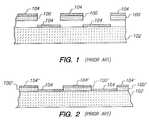
- a diffraction gratingis formed of a multiple mirrored-ribbon structure such as shown in FIG. 1.
- a pattern of a plurality of deformable ribbon structures 100are formed in a spaced relationship over a substrate 102 .
- Both the ribbons and the substrate between the ribbonsare coated with a light reflective material 104 such as an aluminum film.
- the height difference that is designed between the surface of the reflective material 104 on the ribbons 100 and those on the substrate 102is ⁇ /2 when the ribbons are in a relaxed, up state.
- the reflected light from the surface of the ribbons 100will be in phase with the reflected light from the substrate 102 . This is because the light which strikes the substrate travels ⁇ /2 further than the light striking the ribbons and then returns ⁇ /2, for a total of one complete wavelength ⁇ .
- the structureappears as a flat mirror when a beam of light having a wavelength of ⁇ impinges thereon.
- the ribbons 100can be made to bend toward and contact the substrate 102 as shown in FIG. 2 .
- the thickness of the ribbonsis designed to be ⁇ /4. If light at a wavelength ⁇ impinges on this structure perpendicularly to the surface of the substrate 102 , the reflected light from the surface of the ribbons 100 will be completely out of phase with the reflected light from the substrate 102 . This will cause interference between the light from the ribbons and light from the substrate and thus, the structure will diffract the light. Because of the diffraction, the reflected light will come from the surface of the structure at an angle ⁇ from perpendicular.
- FIG. 1can be used to represent a single pixel of a display.
- a typical displaycan contain 1024 ⁇ 1280 pixels arranged in an array of rows and columns.
- a semiconductor device using pixels such as shown in FIG. 1 and having 1024 ⁇ 1280 pixelscan have an array that is approximately 1 inch by 1.3 in extent.
- Such a devicewill likely require at least 2310 I/O structures (1024+1280+6).
- the additional 6 I/O pinsare for specialized biasing.
- the surface area necessary for making connection to such a devicecan exceed the active display area by several times.
- the cost to manufacture the deviceis primarily born by the active display area, such an expense of surface, area is excessive and undesirable. To solve this problem, it is undesirable to manufacture driver structures on the same semiconductor substrate as the active display area. This is due to two primary reasons. First, the cost to manufacture the devices in the active display area is greater than to manufacture electronic circuit components for making drivers using conventional well known techniques. Second, the processing steps are not the same to manufacture the active display area as for electronic circuit components. Thus, a processing specification for such a device would be extremely complex. This would tend to further reduce the yield of such a structure and thereby further increase the cost. For these reasons, it is preferred that the drive electronics be placed in a separate integrated circuit.
- Interconnections to such a devicecould not require the electrically conductive vias nor the bridging technique taught by Rostoker. Further, such an interconnecting structure could not function using a stacked arrangement because light would not be able to impinge onto the surface of the active display area.
- a method of and an apparatus for electrically interconnecting two integrated circuits devicesincludes mounting the two devices face to face.
- a first deviceis mounted for example to a substrate or lead frame.
- the first deviceincludes a plurality of electrical/physical mounting structures preferably positioned along one edge.
- the mounting structuresprovide both electrical interconnection and physical mounting.
- a second deviceincludes a corresponding plurality of mounting structures configured as a mirror image of the mounting structures on the first device.
- the mounting structures on the second deviceare also positioned along one of its edges so that once the mounting structures are brought together in a face to face relationship, the second device cantilevers off the edge of the first device. Under certain circumstances, a dummy block can be mounted to the substrate adjacent to the first device to act as a strut or support for the second device.
- an epoxy potting compoundcan be used to provide structural support.
- the mounting structurescan be positioned sufficiently close to one another that surface area consumed for I/O is minimized.
- Another set of electrical interconnect structurescan be formed on the surface of the second device on the edge opposite the mounting structures. Electrical connection can be formed to these electrical interconnect structures using conventional techniques such as tape automated bonding (TAB) or flex connections.
- TABtape automated bonding
- FIG. 1shows a pixel structure from a prior art semiconductor micromachine display device.
- FIG. 2shows the structure of FIG. 1 under a biased condition.
- FIG. 3shows an exploded partial perspective view of the preferred embodiment of the present invention.
- FIG. 4shows a side view of a first embodiment of the present invention.
- FIG. 5shows a side view of a second embodiment of the present invention.
- FIG. 6shows a side view of a third embodiment of the present invention.
- FIG. 3shows an exploded partial perspective view of the preferred embodiment of the present invention.
- a first semiconductor device 300is substantially planar and includes a primary face 302 and a secondary face 304 .
- An integrated circuit device(not shown) is formed in the primary face 302 of the first semiconductor device 300 .
- the integrated circuit formed on the first semiconductor device 300can be of any type of circuit but is preferably of a semiconductor micromachine display device. However, it will be apparent to one of ordinary skill in the art that the first integrated circuit device 300 could be another conventional circuit such as a microprocessor, controller, PAL, PLA, dynamic or non-volatile memory and the like.
- the first semiconductor device 300is mounted by its secondary surface 304 to a substrate 306 as shown by the dash-dot-dash line.
- the substratecan be of any convenient form such as a printed circuit board, a ceramic or an IC package.
- a plurality of electrical/physical mounting structures 308are formed near one edge on the primary surface 302 of the semiconductor device 300 .
- the mounting structures 308are preferably formed of a metal using conventional semiconductor processing techniques.
- the mounting structures 308are electrically coupled to the integrated circuit (not shown) using conductive traces (either metallic or doped semiconductor).
- the mounting structures 308can be conveniently formed of aluminum or an aluminum alloy. Other metals can also be used.
- a second semiconductor device 310is substantially planar and includes a primary face 312 and a secondary face 314 .
- An integrated circuit device(not shown) is formed in the primary face 312 of the second semiconductor device 310 .
- the integrated circuit formed on the second semiconductor device 310can be of any type of circuit but is preferably of a driver circuit for a semiconductor micromachine display device.
- the second integrated circuit device 310could be another conventional circuit such as a microprocessor, controller, PAL, PLA, dynamic or non-volatile memory and the like.
- the primary surface 312 of the second semiconductor device 310is mounted to the primary surface 302 of the first semiconductor device 300 as shown by the dash-dot-dash line. As can be readily seen the second semiconductor device 310 cantilevers off the edge of the first semiconductor device 300 in an overhanging manner. This limits the amount of the primary surface 302 of the first semiconductor device 300 that is consumed with forming electrical connections to the integrated circuit on the semiconductor device 300 . Because of the techniques described herein, the size of the mounting structures 308 can be as small as 50 microns on a side. The spacing between adjacent mounting structures 308 can be limited to 50 microns.
- a plurality of electrical/physical mounting structures 318are formed near one edge on the primary surface 312 of the semiconductor device 310 .
- the mounting structures 318 and portions of the second semiconductor device 310 along with their respective lead linesare shown as ghost lines to indicate that those structures are hidden from view.
- the mounting structures 318are preferably formed of a metal using conventional semiconductor processing techniques.
- the mounting structures 318are electrically coupled to the integrated circuit (not shown) using conductive traces (either metallic or doped semiconductor).
- the mounting structures 318can be conveniently formed of gold or a solderable alloy. Other metals can also be used.
- the mounting structures 318 formed in the second semiconductor device 310are configured in a mirror image to the mounting structures 308 that are formed on the first semiconductor device 300 . In this way, when the first semiconductor device 300 and the semiconductor device 310 are brought together in a face to face relation, the mounting structures 308 and 318 will join together electrically and physically.
- FIG. 4shows a side view of the structure of FIG. 3 .
- the same reference numeralswill be used to identify identical structures to avoid obscuring the invention in extraneous detail.
- FIG. 4also shows an electrical interconnection made from other systems to the second semiconductor device 310 .
- a second plurality of mounting structures 320are formed on the primary surface 312 of the second semiconductor device 310 .
- the mounting structuresare located on an edge opposite those of the mounting structures 318 .
- the size and spacing of the second plurality of mounting structures 320need not be identical to that for the mounting structures 318 .
- a flexible tape connector 322includes a corresponding set of mounting structures 324 that are configured as a mirror image to those of the mounting structures 320 .
- the flexible tape connector 322is coupled to the second semiconductor device 310 in the conventional manner.
- the first and the second semiconductor devices 300 and 310are formed using semiconductor processing steps known and described in detail elsewhere.
- Either the mounting structures 308 or the mounting structures 318 or bothinclude a mounting substance such as solder.
- the first semiconductor device 300is mounted to the substrate 306 .
- a flexible tape connector 322is mounted to the second semiconductor device 310 .
- the second semiconductor device 310 with the flexible tape connector 322are brought to the first semiconductor device 300 .
- the mounting substanceis melted with heat or ultrasonically to join the mounting structures 308 and 318 electrically and physically.
- a support structure 330is used as shown in FIG. 5 .
- the support structure 330is mounted adjacent the edge of the first semiconductor device 300 to which the second semiconductor device 310 is mounted.
- the support structure 330can be formed of a dummy block of semiconductor material or can be formed of a defective/non-functioning device such as the first semiconductor device 300 . It is desirable that the height of the support structure 330 approximate that of the first semiconductor device 300 .
- An adhesive material 332is placed on an upper surface of the support structure 330 to hold the second semiconductor device 310 in place.
- the adhesive 332is formed of a compressible material so that it will conform to an ideal height for supporting the second semiconductor device 310 .
- a potting compound 340can be used as shown in FIG. 6 .
- an epoxy potting compoundis used.
- the support structure 330 shown in FIG. 5can be replaced with the potting compound 340 .
- the potting compound 340is mounted adjacent the edge of the first semiconductor device 300 to which the second semiconductor device 310 is mounted.
- the electrical interconnection 322is coupled to the second semiconductor device 310 before the potting compound is applied.
- the potting compound 340can be limited to the region under the second semiconductor device 310 , can extend up and over the second semiconductor device 310 as shown at reference numeral 340 ′ or in between. Because the preferred embodiment of the present invention is intended for applications wherein the first semiconductor device 300 is configured to reflect light, it is important in such applications that the potting compound 340 and/or 340 ′ not cover the first semiconductor device 300 .
Landscapes
- Engineering & Computer Science (AREA)
- Microelectronics & Electronic Packaging (AREA)
- Power Engineering (AREA)
- Physics & Mathematics (AREA)
- Condensed Matter Physics & Semiconductors (AREA)
- General Physics & Mathematics (AREA)
- Computer Hardware Design (AREA)
- Manufacturing & Machinery (AREA)
- Wire Bonding (AREA)
- Micromachines (AREA)
- Diffracting Gratings Or Hologram Optical Elements (AREA)
- Combinations Of Printed Boards (AREA)
Abstract
Description
This application is a divisional of U.S. patent application Ser. No. 08/920,122, filed on Sep. 2, 1997, now U.S. Pat. No. 6,096,576 the contents of which are hereby incorporated by reference.
This invention relates to the field of forming electrical connections to integrated circuit devices. More particularly, this invention relates to forming an extremely large number of electrical connections to an integrated circuit using an inverted interface integrated circuit.
As important as manufacturing an integrated circuit is the ability to apply electronic signals to and receive electronic signals from the integrated circuit. Ordinarily, an integrated circuit die is configured to have relatively large exposed metal areas, known as bonding pads, through which this electrical interface can be conducted. Often these metal areas are formed of aluminum or an aluminum alloy, which can for example 5 mils, square.
Several well known techniques are commercially used to realize such electrical interface. One such well known technique is conventionally called wire bonding. The completed die is mounted to a lead frame which is integral to the package, such as a dual-in-line package (DIP), pin grid array package (PGA), or other packages equally well known. The package includes individual pins or other electrical contact devices that are configured for ready coupling to an external circuit or circuit board through soldering, socketing or other well known means. Electrical contact is made between the bonding pads and the lead frame by attaching a thin wire between these contacts. The wire is attached to the bonding pads and the lead frame by heating or ultrasonically welding the wire to the pads. Unfortunately, the bonding wire introduces impedance into the path of an electric signal due to its thinness and length. The bonding wire acts as an inductor. This impedance operates to add noise to the signal, thereby decreasing the overall operating efficiency of a system including bonding wires. Further, because of the physical requirements of the wire and the potential for undesired contact between adjacent wires, the spacing requirements are restrictive. The bonding pads are positioned near the edges of the die to allow a shortest path for the bonding wire. The bonding wire can also act as an antenna.
Another well known technique is commonly known as flip chip bonding. According to flip chip bonding, a substrate such as a printed circuit board includes electrically conductive lands that are formed into a mirror image of the bonding pads on an integrated circuit. Generally, the bonding pads are treated with a layer of solder. The integrated circuit and the substrate are mounted in a face-to-face relation to one another and the solder is melted with heat to join the bonding pads and to the corresponding land. In this way, the bonding pads and the lands necessarily provide electrical contact from the integrated circuit to the substrate. Unfortunately, electrical interconnection between two integrated circuits on a printed circuit board, each die using flip chip bonding, requires signal traces along the substrate. These traces, such as on a printed circuit board, introduce impedance into the path of the electric signals and operate to slow the transmission of the signals, thereby decreasing the overall operating efficiency of such a system.
Others have proposed chip to chip bonding techniques. For example, U.S. Pat. No. 5,399,898 to Rostoker discloses a multi-chip semiconductor arrangement using flip chip dies. Rostoker teaches arrangements using double sided flip chips which have raised bumps on both sides and single sided flip chips which have raised bumps on one side. The double sided flip chips are mounted on the substrate and the single sided flip chips bridge the gap between the double sided flip chips with minimal overlap. The Rostoker invention suffers from the several difficulties in implementation. For example, an upper integrated circuit must be mounted as a bridge between two integrated circuit dice. This requires such an assembly to consume considerable surface area on a substrate such as a printed circuit board, or requires an atypically large integrated circuit package to contain such an assembly. In addition, the upper integrated circuit must be manufactured using complex processing techniques that form electrically conductive vias through the body of that integrated circuit. Such techniques are complex and thus expensive to perform. Electrical connection to this assembly is made to the back of the upper integrated circuit using for example conventional wire bonding techniques.
Still others have proposed techniques for reducing the volume and thus surface area consumed by multiple integrated circuit devices. One such technique is taught in U.S. Pat. No. 5,491,612 to Nicewarner, Jr. This technique is not concerned with the number of interconnections between integrated circuits but rather the volume of space consumed by plural integrated circuits. Nicewarner teaches a three dimensional modular assembly of integrated circuits. The chips are mounted back to back and are mounted on both sides of the primary substrate and between each of the two secondary substrates and the primary substrate. Because of the design, the array of chips between the primary substrate and the first secondary substrate must mirror the array of chips between the primary substrate and the second secondary substrate.
Yet others have proposed stacking integrated circuits one on top of another. Such techniques include forming interconnections along the sides of the stack. Heat dissipation from an integrated circuit within the stack can become a problem.
An emerging technology surrounds semiconductor micromachines that are used for forming displays. A device that can be used for such a display is disclosed in U.S. Pat. No. 5,311,360 which is incorporated in its entirety herein by reference.
According to the teachings of the '360 patent, a diffraction grating is formed of a multiple mirrored-ribbon structure such as shown in FIG. 1. A pattern of a plurality ofdeformable ribbon structures 100 are formed in a spaced relationship over asubstrate 102. Both the ribbons and the substrate between the ribbons are coated with a lightreflective material 104 such as an aluminum film. The height difference that is designed between the surface of thereflective material 104 on theribbons 100 and those on thesubstrate 102 is λ/2 when the ribbons are in a relaxed, up state. If light at a wavelength λ impinges on this structure perpendicularly to the surface of thesubstrate 102, the reflected light from the surface of theribbons 100 will be in phase with the reflected light from thesubstrate 102. This is because the light which strikes the substrate travels λ/2 further than the light striking the ribbons and then returns λ/2, for a total of one complete wavelength λ. Thus, the structure appears as a flat mirror when a beam of light having a wavelength of λ impinges thereon.
By applying appropriate voltages to theribbons 100 and thesubstrate 102, theribbons 100 can be made to bend toward and contact thesubstrate 102 as shown in FIG.2. The thickness of the ribbons is designed to be λ/4. If light at a wavelength λ impinges on this structure perpendicularly to the surface of thesubstrate 102, the reflected light from the surface of theribbons 100 will be completely out of phase with the reflected light from thesubstrate 102. This will cause interference between the light from the ribbons and light from the substrate and thus, the structure will diffract the light. Because of the diffraction, the reflected light will come from the surface of the structure at an angle Θ from perpendicular.
It will become apparent to one of ordinary skill in the art after studying the teachings of the '360 patent that the structure shown in FIG. 1 can be used to represent a single pixel of a display. A typical display can contain 1024×1280 pixels arranged in an array of rows and columns. A semiconductor device using pixels such as shown in FIG.1 and having 1024×1280 pixels can have an array that is approximately 1 inch by 1.3 in extent. Such a device will likely require at least 2310 I/O structures (1024+1280+6). The additional 6 I/O pins are for specialized biasing. Using conventional wire bonding bond pad structures, the surface area necessary for making connection to such a device can exceed the active display area by several times. Because the cost to manufacture the device is primarily born by the active display area, such an expense of surface, area is excessive and undesirable. To solve this problem, it is undesirable to manufacture driver structures on the same semiconductor substrate as the active display area. This is due to two primary reasons. First, the cost to manufacture the devices in the active display area is greater than to manufacture electronic circuit components for making drivers using conventional well known techniques. Second, the processing steps are not the same to manufacture the active display area as for electronic circuit components. Thus, a processing specification for such a device would be extremely complex. This would tend to further reduce the yield of such a structure and thereby further increase the cost. For these reasons, it is preferred that the drive electronics be placed in a separate integrated circuit.
Interconnections to such a device could not require the electrically conductive vias nor the bridging technique taught by Rostoker. Further, such an interconnecting structure could not function using a stacked arrangement because light would not be able to impinge onto the surface of the active display area.
What is needed is a method of and apparatus for providing electrical interconnections directly from one integrated circuit to another.
What is also needed is a method of and an apparatus for providing electrical interconnections to an integrated circuit with extremely high I/O requirements.
What is further needed is a method of and an apparatus for providing electrical interconnections to an integrated circuit without obscuring the surface of the integrated circuit.
A method of and an apparatus for electrically interconnecting two integrated circuits devices includes mounting the two devices face to face. A first device is mounted for example to a substrate or lead frame. The first device includes a plurality of electrical/physical mounting structures preferably positioned along one edge. The mounting structures provide both electrical interconnection and physical mounting. A second device includes a corresponding plurality of mounting structures configured as a mirror image of the mounting structures on the first device. The mounting structures on the second device are also positioned along one of its edges so that once the mounting structures are brought together in a face to face relationship, the second device cantilevers off the edge of the first device. Under certain circumstances, a dummy block can be mounted to the substrate adjacent to the first device to act as a strut or support for the second device. Under certain other circumstances, an epoxy potting compound can be used to provide structural support. The mounting structures can be positioned sufficiently close to one another that surface area consumed for I/O is minimized. Another set of electrical interconnect structures can be formed on the surface of the second device on the edge opposite the mounting structures. Electrical connection can be formed to these electrical interconnect structures using conventional techniques such as tape automated bonding (TAB) or flex connections.
FIG. 1 shows a pixel structure from a prior art semiconductor micromachine display device.
FIG. 2 shows the structure of FIG. 1 under a biased condition.
FIG. 3 shows an exploded partial perspective view of the preferred embodiment of the present invention.
FIG. 4 shows a side view of a first embodiment of the present invention.
FIG. 5 shows a side view of a second embodiment of the present invention.
FIG. 6 shows a side view of a third embodiment of the present invention.
FIG. 3 shows an exploded partial perspective view of the preferred embodiment of the present invention. Afirst semiconductor device 300 is substantially planar and includes aprimary face 302 and asecondary face 304. An integrated circuit device (not shown) is formed in theprimary face 302 of thefirst semiconductor device 300. The integrated circuit formed on thefirst semiconductor device 300 can be of any type of circuit but is preferably of a semiconductor micromachine display device. However, it will be apparent to one of ordinary skill in the art that the firstintegrated circuit device 300 could be another conventional circuit such as a microprocessor, controller, PAL, PLA, dynamic or non-volatile memory and the like.
Thefirst semiconductor device 300 is mounted by itssecondary surface 304 to asubstrate 306 as shown by the dash-dot-dash line. The substrate can be of any convenient form such as a printed circuit board, a ceramic or an IC package. A plurality of electrical/physical mountingstructures 308 are formed near one edge on theprimary surface 302 of thesemiconductor device 300. The mountingstructures 308 are preferably formed of a metal using conventional semiconductor processing techniques. The mountingstructures 308 are electrically coupled to the integrated circuit (not shown) using conductive traces (either metallic or doped semiconductor). The mountingstructures 308 can be conveniently formed of aluminum or an aluminum alloy. Other metals can also be used.
Asecond semiconductor device 310 is substantially planar and includes aprimary face 312 and asecondary face 314. An integrated circuit device (not shown) is formed in theprimary face 312 of thesecond semiconductor device 310. The integrated circuit formed on thesecond semiconductor device 310 can be of any type of circuit but is preferably of a driver circuit for a semiconductor micromachine display device. However, it will be apparent to one of ordinary skill in the art that the secondintegrated circuit device 310 could be another conventional circuit such as a microprocessor, controller, PAL, PLA, dynamic or non-volatile memory and the like.
Theprimary surface 312 of thesecond semiconductor device 310 is mounted to theprimary surface 302 of thefirst semiconductor device 300 as shown by the dash-dot-dash line. As can be readily seen thesecond semiconductor device 310 cantilevers off the edge of thefirst semiconductor device 300 in an overhanging manner. This limits the amount of theprimary surface 302 of thefirst semiconductor device 300 that is consumed with forming electrical connections to the integrated circuit on thesemiconductor device 300. Because of the techniques described herein, the size of the mountingstructures 308 can be as small as 50 microns on a side. The spacing between adjacent mountingstructures 308 can be limited to 50 microns.
A plurality of electrical/physical mountingstructures 318 are formed near one edge on theprimary surface 312 of thesemiconductor device 310. The mountingstructures 318 and portions of thesecond semiconductor device 310 along with their respective lead lines are shown as ghost lines to indicate that those structures are hidden from view. The mountingstructures 318 are preferably formed of a metal using conventional semiconductor processing techniques. The mountingstructures 318 are electrically coupled to the integrated circuit (not shown) using conductive traces (either metallic or doped semiconductor). The mountingstructures 318 can be conveniently formed of gold or a solderable alloy. Other metals can also be used.
The mountingstructures 318 formed in thesecond semiconductor device 310 are configured in a mirror image to the mountingstructures 308 that are formed on thefirst semiconductor device 300. In this way, when thefirst semiconductor device 300 and thesemiconductor device 310 are brought together in a face to face relation, the mountingstructures
FIG. 4 shows a side view of the structure of FIG.3. Where appropriate, the same reference numerals will be used to identify identical structures to avoid obscuring the invention in extraneous detail. Note that a large portion of thefirst semiconductor device 300 is exposed. This is particularly ideal for the preferred embodiment of the present invention where the integrated circuit is a semiconductor micromachine display device. Under such circumstances, it is essential that the integrated circuit be exposed to receive and reflect or diffract light.
In addition to the structural elements discussed above relative to FIG. 3, FIG. 4 also shows an electrical interconnection made from other systems to thesecond semiconductor device 310. A second plurality of mountingstructures 320 are formed on theprimary surface 312 of thesecond semiconductor device 310. Preferably, the mounting structures are located on an edge opposite those of the mountingstructures 318. As shown, the size and spacing of the second plurality of mountingstructures 320 need not be identical to that for the mountingstructures 318. Aflexible tape connector 322 includes a corresponding set of mountingstructures 324 that are configured as a mirror image to those of the mountingstructures 320. Theflexible tape connector 322 is coupled to thesecond semiconductor device 310 in the conventional manner.
The process for forming the structure of FIGS. 3 and 4 follows. Separately, the first and thesecond semiconductor devices structures 308 or the mountingstructures 318 or both include a mounting substance such as solder. Once completed, thefirst semiconductor device 300 is mounted to thesubstrate 306. Separately, aflexible tape connector 322 is mounted to thesecond semiconductor device 310. Once these two subassemblies are formed, thesecond semiconductor device 310 with theflexible tape connector 322 are brought to thefirst semiconductor device 300. The mounting substance is melted with heat or ultrasonically to join the mountingstructures
Under certain circumstances, it may be determined that the strength of the joined mountingstructures second semiconductor device 310 in place without failing. Under those circumstances asupport structure 330 is used as shown in FIG.5. Thesupport structure 330 is mounted adjacent the edge of thefirst semiconductor device 300 to which thesecond semiconductor device 310 is mounted. Thesupport structure 330 can be formed of a dummy block of semiconductor material or can be formed of a defective/non-functioning device such as thefirst semiconductor device 300. It is desirable that the height of thesupport structure 330 approximate that of thefirst semiconductor device 300. Anadhesive material 332 is placed on an upper surface of thesupport structure 330 to hold thesecond semiconductor device 310 in place. Preferably, the adhesive332 is formed of a compressible material so that it will conform to an ideal height for supporting thesecond semiconductor device 310.
As an alternative to the structure shown in FIG. 5, where it is determined that the strength of the joined mountingstructures second semiconductor device 310 in place without failing, apotting compound 340 can be used as shown in FIG.6. Preferably, an epoxy potting compound is used. Under those circumstances, thesupport structure 330 shown in FIG. 5 can be replaced with thepotting compound 340. Like thesupport structure 330, thepotting compound 340 is mounted adjacent the edge of thefirst semiconductor device 300 to which thesecond semiconductor device 310 is mounted. Preferably, theelectrical interconnection 322 is coupled to thesecond semiconductor device 310 before the potting compound is applied. Thepotting compound 340 can be limited to the region under thesecond semiconductor device 310, can extend up and over thesecond semiconductor device 310 as shown atreference numeral 340′ or in between. Because the preferred embodiment of the present invention is intended for applications wherein thefirst semiconductor device 300 is configured to reflect light, it is important in such applications that thepotting compound 340 and/or340′ not cover thefirst semiconductor device 300.
The present invention has been described in terms of specific embodiments incorporating details to facilitate the understanding of the principles of construction and operation of the invention. Such reference herein to specific embodiments and details thereof is not intended to limit the scope of the claims appended hereto. It will be apparent to those skilled in the art that modifications may be made in the embodiments chosen for illustration without departing from the spirit and scope of the invention.
Specifically, it will be apparent to one of ordinary skill in the art that the device of the present invention could be implemented in several different ways and the apparatus disclosed above is only illustrative of the preferred embodiment of the invention and is in no way a limitation. For example, it would be within the scope of the invention to vary the materials and structures of the various components disclosed herein.
Claims (12)
1. An electrical system comprising:
a. a first substantially planar substrate having a first primary surface, having a first integrated circuit formed in the first primary surface, and having a secondary surface opposite to the first primary surface, wherein a first plurality of integrated circuit electrical contacts are positioned along a first edge of the first primary surface;
b. a second substantially planar substrate having a second primary surface, and having a second integrated circuit formed in the second primary surface, the second primary surface having a third edge opposite a second edge, wherein a second plurality of integrated circuit electrical contacts are positioned along the second edge of the second primary surface; and
c. an electrical interface for electrically coupling the first plurality of integrated circuit electrical contacts in a face to face relationship with the second plurality of integrated circuit electrical contacts such that the first substantially planar substrate overlaps the second substantially planar substrate only in a region of the first and second integrated circuit electrical contacts but is not substantially overlapping otherwise such that the third edge is substantially unsupported wherein the second substantially planar substrate cantilevers off the edge of the first substantially planar substrate.
2. The electrical system according toclaim 1 wherein the first integrated circuit comprises a multiple mirrored-ribbon structure and wherein the second integrated circuit comprises a driver circuit for coupling to and controlling the first integrated circuit.
3. The electrical system according toclaim 1 further comprising a third substantially planar substrate wherein the first secondary surface is mounted to the third substantially planar substrate.
4. The electrical system according toclaim 1 further comprising a third plurality of integrated circuit electrical contacts positioned along the third edge for coupling to a flexible tape structure.
5. The electrical system according toclaim 1 wherein each of the first and second pluralities of integrated circuit electrical contacts are positioned sufficiently close to one another that a minimum surface area is consumed for input/output circuitry.
6. The electrical system according toclaim 1 further comprising a non-electrical support structure coupled to and mounted underneath the second substantially planar substrate to hold the second substantially planar substrate in place.
7. A cantilevered flip-chip assembly for exposing a multiple mirrored ribbon structure formed on a surface of a semiconductor substrate and for coupling the multiple mirrored ribbon structure to a driver circuit, wherein the multiple mirrored-ribbon structure is controlled by the deliver circuit, the cantilevered flip-chip assembly comprising:
a. a first substantially planar substrate having a first surface on which first circuit elements including the multiple mirrored-ribbon structure are formed, wherein a first plurality of integrated circuit electrical contacts are positioned along a first edge of the first primary surface and coupled to the first circuit elements; and
b. a second substantially planar substrate having a second surface on which second circuit elements including the driver circuit are formed, the second primary surface having a third edge opposite a second edge, wherein a second plurality of integrated circuit electrical contacts are positioned along the second edge of the second primary surface for coupling to the first plurality of integrated circuit electrical contacts in a face to face relationship such that the second substantially planar substrate partially overlaps the first substantially planar substrate in a region of the first and second plurality of integrated circuit electrical contacts.
8. The cantilevered flip-chip assembly according toclaim 7 further comprising a third plurality of integrated circuit electrical contacts positioned along the third edge of the second substantially planar substrate for coupling to a flexible tape structure and for making external connections to other integrated circuits.
9. The cantilevered flip-chip assembly according toclaim 7 further comprising a non-electrical support structure coupled to and mounted underneath the second substantially planar substrate for holding the second substantially planar substrate in place.
10. The cantilevered flip-chip assembly according toclaim 9 wherein the non-electrical support structure is formed of a block of semiconductor material.
11. The cantilevered flip-chip assembly according toclaim 10 wherein the non-electrical support structure is formed of a potting compound.
12. The cantilevered flip-chip assembly according toclaim 11 wherein the potting compound is an epoxy potting compound.
Priority Applications (1)
| Application Number | Priority Date | Filing Date | Title |
|---|---|---|---|
| US09/500,118US6452260B1 (en) | 1997-09-02 | 2000-02-08 | Electrical interface to integrated circuit device having high density I/O count |
Applications Claiming Priority (2)
| Application Number | Priority Date | Filing Date | Title |
|---|---|---|---|
| US08/920,122US6096576A (en) | 1997-09-02 | 1997-09-02 | Method of producing an electrical interface to an integrated circuit device having high density I/O count |
| US09/500,118US6452260B1 (en) | 1997-09-02 | 2000-02-08 | Electrical interface to integrated circuit device having high density I/O count |
Related Parent Applications (1)
| Application Number | Title | Priority Date | Filing Date |
|---|---|---|---|
| US08/920,122DivisionUS6096576A (en) | 1997-09-02 | 1997-09-02 | Method of producing an electrical interface to an integrated circuit device having high density I/O count |
Publications (1)
| Publication Number | Publication Date |
|---|---|
| US6452260B1true US6452260B1 (en) | 2002-09-17 |
Family
ID=25443205
Family Applications (2)
| Application Number | Title | Priority Date | Filing Date |
|---|---|---|---|
| US08/920,122Expired - LifetimeUS6096576A (en) | 1997-09-02 | 1997-09-02 | Method of producing an electrical interface to an integrated circuit device having high density I/O count |
| US09/500,118Expired - LifetimeUS6452260B1 (en) | 1997-09-02 | 2000-02-08 | Electrical interface to integrated circuit device having high density I/O count |
Family Applications Before (1)
| Application Number | Title | Priority Date | Filing Date |
|---|---|---|---|
| US08/920,122Expired - LifetimeUS6096576A (en) | 1997-09-02 | 1997-09-02 | Method of producing an electrical interface to an integrated circuit device having high density I/O count |
Country Status (8)
| Country | Link |
|---|---|
| US (2) | US6096576A (en) |
| EP (1) | EP1021834A1 (en) |
| JP (1) | JP2001515276A (en) |
| KR (1) | KR20010023575A (en) |
| CN (1) | CN1278365A (en) |
| AU (1) | AU7987998A (en) |
| NO (1) | NO20001038L (en) |
| WO (1) | WO1999012208A1 (en) |
Cited By (41)
| Publication number | Priority date | Publication date | Assignee | Title |
|---|---|---|---|---|
| US20040026771A1 (en)* | 2001-09-10 | 2004-02-12 | Layman Paul Arthur | High-density inter-die interconnect structure |
| US6707591B2 (en) | 2001-04-10 | 2004-03-16 | Silicon Light Machines | Angled illumination for a single order light modulator based projection system |
| US6712480B1 (en) | 2002-09-27 | 2004-03-30 | Silicon Light Machines | Controlled curvature of stressed micro-structures |
| US6714337B1 (en) | 2002-06-28 | 2004-03-30 | Silicon Light Machines | Method and device for modulating a light beam and having an improved gamma response |
| US6728023B1 (en) | 2002-05-28 | 2004-04-27 | Silicon Light Machines | Optical device arrays with optimized image resolution |
| US6747781B2 (en) | 2001-06-25 | 2004-06-08 | Silicon Light Machines, Inc. | Method, apparatus, and diffuser for reducing laser speckle |
| US6764875B2 (en) | 1998-07-29 | 2004-07-20 | Silicon Light Machines | Method of and apparatus for sealing an hermetic lid to a semiconductor die |
| US6767751B2 (en) | 2002-05-28 | 2004-07-27 | Silicon Light Machines, Inc. | Integrated driver process flow |
| US6782205B2 (en) | 2001-06-25 | 2004-08-24 | Silicon Light Machines | Method and apparatus for dynamic equalization in wavelength division multiplexing |
| US6800238B1 (en) | 2002-01-15 | 2004-10-05 | Silicon Light Machines, Inc. | Method for domain patterning in low coercive field ferroelectrics |
| US6801354B1 (en) | 2002-08-20 | 2004-10-05 | Silicon Light Machines, Inc. | 2-D diffraction grating for substantially eliminating polarization dependent losses |
| US6806997B1 (en) | 2003-02-28 | 2004-10-19 | Silicon Light Machines, Inc. | Patterned diffractive light modulator ribbon for PDL reduction |
| US6813059B2 (en) | 2002-06-28 | 2004-11-02 | Silicon Light Machines, Inc. | Reduced formation of asperities in contact micro-structures |
| US6822797B1 (en) | 2002-05-31 | 2004-11-23 | Silicon Light Machines, Inc. | Light modulator structure for producing high-contrast operation using zero-order light |
| US6829077B1 (en) | 2003-02-28 | 2004-12-07 | Silicon Light Machines, Inc. | Diffractive light modulator with dynamically rotatable diffraction plane |
| US6829092B2 (en) | 2001-08-15 | 2004-12-07 | Silicon Light Machines, Inc. | Blazed grating light valve |
| US6829258B1 (en) | 2002-06-26 | 2004-12-07 | Silicon Light Machines, Inc. | Rapidly tunable external cavity laser |
| US6865346B1 (en) | 2001-06-05 | 2005-03-08 | Silicon Light Machines Corporation | Fiber optic transceiver |
| US6872984B1 (en) | 1998-07-29 | 2005-03-29 | Silicon Light Machines Corporation | Method of sealing a hermetic lid to a semiconductor die at an angle |
| US6908201B2 (en) | 2002-06-28 | 2005-06-21 | Silicon Light Machines Corporation | Micro-support structures |
| US6922273B1 (en) | 2003-02-28 | 2005-07-26 | Silicon Light Machines Corporation | PDL mitigation structure for diffractive MEMS and gratings |
| US6922272B1 (en) | 2003-02-14 | 2005-07-26 | Silicon Light Machines Corporation | Method and apparatus for leveling thermal stress variations in multi-layer MEMS devices |
| US6928207B1 (en) | 2002-12-12 | 2005-08-09 | Silicon Light Machines Corporation | Apparatus for selectively blocking WDM channels |
| US6927891B1 (en) | 2002-12-23 | 2005-08-09 | Silicon Light Machines Corporation | Tilt-able grating plane for improved crosstalk in 1×N blaze switches |
| US6934070B1 (en) | 2002-12-18 | 2005-08-23 | Silicon Light Machines Corporation | Chirped optical MEM device |
| US6947613B1 (en) | 2003-02-11 | 2005-09-20 | Silicon Light Machines Corporation | Wavelength selective switch and equalizer |
| US6956995B1 (en) | 2001-11-09 | 2005-10-18 | Silicon Light Machines Corporation | Optical communication arrangement |
| US6956878B1 (en) | 2000-02-07 | 2005-10-18 | Silicon Light Machines Corporation | Method and apparatus for reducing laser speckle using polarization averaging |
| US6987600B1 (en) | 2002-12-17 | 2006-01-17 | Silicon Light Machines Corporation | Arbitrary phase profile for better equalization in dynamic gain equalizer |
| US6991953B1 (en) | 2001-09-13 | 2006-01-31 | Silicon Light Machines Corporation | Microelectronic mechanical system and methods |
| US7027202B1 (en) | 2003-02-28 | 2006-04-11 | Silicon Light Machines Corp | Silicon substrate as a light modulator sacrificial layer |
| US7042611B1 (en) | 2003-03-03 | 2006-05-09 | Silicon Light Machines Corporation | Pre-deflected bias ribbons |
| US7054515B1 (en) | 2002-05-30 | 2006-05-30 | Silicon Light Machines Corporation | Diffractive light modulator-based dynamic equalizer with integrated spectral monitor |
| US7057819B1 (en) | 2002-12-17 | 2006-06-06 | Silicon Light Machines Corporation | High contrast tilting ribbon blazed grating |
| US7057795B2 (en) | 2002-08-20 | 2006-06-06 | Silicon Light Machines Corporation | Micro-structures with individually addressable ribbon pairs |
| US7068372B1 (en) | 2003-01-28 | 2006-06-27 | Silicon Light Machines Corporation | MEMS interferometer-based reconfigurable optical add-and-drop multiplexor |
| US7102240B2 (en) | 2004-06-11 | 2006-09-05 | Samsung Electro-Mechanics Co., Ltd. | Embedded integrated circuit packaging structure |
| US7177081B2 (en) | 2001-03-08 | 2007-02-13 | Silicon Light Machines Corporation | High contrast grating light valve type device |
| US7286764B1 (en) | 2003-02-03 | 2007-10-23 | Silicon Light Machines Corporation | Reconfigurable modulator-based optical add-and-drop multiplexer |
| US7391973B1 (en) | 2003-02-28 | 2008-06-24 | Silicon Light Machines Corporation | Two-stage gain equalizer |
| US8674494B2 (en) | 2011-08-31 | 2014-03-18 | Samsung Electronics Co., Ltd. | Semiconductor package having supporting plate and method of forming the same |
Families Citing this family (12)
| Publication number | Priority date | Publication date | Assignee | Title |
|---|---|---|---|---|
| US6096576A (en)* | 1997-09-02 | 2000-08-01 | Silicon Light Machines | Method of producing an electrical interface to an integrated circuit device having high density I/O count |
| JP3565319B2 (en)* | 1999-04-14 | 2004-09-15 | シャープ株式会社 | Semiconductor device and manufacturing method thereof |
| US6570250B1 (en)* | 2000-02-24 | 2003-05-27 | Honeywell International Inc. | Power conditioning substrate stiffener |
| US6785001B2 (en) | 2001-08-21 | 2004-08-31 | Silicon Light Machines, Inc. | Method and apparatus for measuring wavelength jitter of light signal |
| US6839479B2 (en) | 2002-05-29 | 2005-01-04 | Silicon Light Machines Corporation | Optical switch |
| JP3819851B2 (en)* | 2003-01-29 | 2006-09-13 | 松下電器産業株式会社 | Semiconductor device and manufacturing method thereof |
| US7046420B1 (en) | 2003-02-28 | 2006-05-16 | Silicon Light Machines Corporation | MEM micro-structures and methods of making the same |
| US7163155B2 (en)* | 2003-11-05 | 2007-01-16 | Interdigital Technology Corporation | ASIC-embedded switchable antenna arrays |
| JP4580730B2 (en)* | 2003-11-28 | 2010-11-17 | ルネサスエレクトロニクス株式会社 | Offset junction type multi-chip semiconductor device |
| CN100416807C (en)* | 2004-10-20 | 2008-09-03 | 力晶半导体股份有限公司 | Semiconductor package structure and manufacturing method thereof |
| WO2014122882A1 (en) | 2013-02-05 | 2014-08-14 | パナソニック株式会社 | Semiconductor device |
| IT201700103511A1 (en) | 2017-09-15 | 2019-03-15 | St Microelectronics Srl | MICROELECTRONIC DEVICE EQUIPPED WITH PROTECTED CONNECTIONS AND RELATIVE PROCESS OF MANUFACTURE |
Citations (101)
| Publication number | Priority date | Publication date | Assignee | Title |
|---|---|---|---|---|
| US3256465A (en) | 1962-06-08 | 1966-06-14 | Signetics Corp | Semiconductor device assembly with true metallurgical bonds |
| US3388301A (en) | 1964-12-09 | 1968-06-11 | Signetics Corp | Multichip integrated circuit assembly with interconnection structure |
| US3657610A (en) | 1969-07-10 | 1972-04-18 | Nippon Electric Co | Self-sealing face-down bonded semiconductor device |
| US3811186A (en) | 1972-12-11 | 1974-05-21 | Ibm | Method of aligning and attaching circuit devices on a substrate |
| US3871014A (en) | 1969-08-14 | 1975-03-11 | Ibm | Flip chip module with non-uniform solder wettable areas on the substrate |
| US3942245A (en) | 1971-11-20 | 1976-03-09 | Ferranti Limited | Related to the manufacture of lead frames and the mounting of semiconductor devices thereon |
| US4012835A (en) | 1974-09-17 | 1977-03-22 | E. I. Du Pont De Nemours And Co. | Method of forming a dual in-line package |
| US4021766A (en) | 1975-07-28 | 1977-05-03 | Aine Harry E | Solid state pressure transducer of the leaf spring type and batch method of making same |
| US4034399A (en) | 1976-02-27 | 1977-07-05 | Rca Corporation | Interconnection means for an array of majority carrier microwave devices |
| JPS5339068A (en) | 1976-09-22 | 1978-04-10 | Hitachi Ltd | Semiconductor device |
| US4103273A (en) | 1973-04-26 | 1978-07-25 | Honeywell Inc. | Method for batch fabricating semiconductor devices |
| US4190855A (en) | 1976-08-11 | 1980-02-26 | Sharp Kabushiki Kaisha | Installation of a semiconductor chip on a glass substrate |
| JPS55111151A (en) | 1979-02-20 | 1980-08-27 | Nec Corp | Integrated circuit device |
| JPS5731166A (en) | 1980-07-31 | 1982-02-19 | Fujitsu Ltd | Semiconductor device |
| US4355463A (en) | 1980-03-24 | 1982-10-26 | National Semiconductor Corporation | Process for hermetically encapsulating semiconductor devices |
| JPS57210638A (en) | 1981-06-18 | 1982-12-24 | Mitsubishi Electric Corp | Hybrid integrated circuit |
| DE3233195A1 (en) | 1981-09-08 | 1983-03-17 | Mitsubishi Denki K.K., Tokyo | Semiconductor device |
| EP0089044A2 (en) | 1982-03-16 | 1983-09-21 | Nec Corporation | A semiconductor device having a container sealed with a solder of low melting point |
| GB2117564A (en) | 1982-03-26 | 1983-10-12 | Int Computers Ltd | Mounting one integrated circuit upon another |
| US4417386A (en) | 1980-01-17 | 1983-11-29 | Siemens Aktiengesellschaft | Method for mounting a semiconductor device in a housing |
| US4426768A (en) | 1981-12-28 | 1984-01-24 | United Technologies Corporation | Ultra-thin microelectronic pressure sensors |
| US4467342A (en) | 1982-07-15 | 1984-08-21 | Rca Corporation | Multi-chip imager |
| JPS6049638A (en) | 1983-08-26 | 1985-03-18 | Sharp Corp | Construction of electronic parts |
| JPS6094756A (en) | 1983-10-29 | 1985-05-27 | Toshiba Corp | semiconductor equipment |
| US4545610A (en) | 1983-11-25 | 1985-10-08 | International Business Machines Corporation | Method for forming elongated solder connections between a semiconductor device and a supporting substrate |
| JPS60250639A (en) | 1984-05-25 | 1985-12-11 | Nec Kansai Ltd | Hybrid ic |
| JPS61142750A (en) | 1985-11-22 | 1986-06-30 | Hitachi Ltd | insulation board |
| JPS61145838A (en) | 1984-12-20 | 1986-07-03 | Fujitsu Ltd | How to connect semiconductor elements |
| US4700276A (en) | 1986-01-03 | 1987-10-13 | Motorola Inc. | Ultra high density pad array chip carrier |
| US4717066A (en) | 1986-02-24 | 1988-01-05 | American Telephone And Telegraph Company, At&T Bell Laboratories | Method of bonding conductors to semiconductor devices |
| US4721629A (en) | 1983-06-21 | 1988-01-26 | Sanyo Electric Co., Ltd. | Method of manufacturing photovoltaic device |
| US4804641A (en) | 1985-09-30 | 1989-02-14 | Siemens Aktiengesellschaft | Method for limiting chippage when sawing a semiconductor wafer |
| US4807021A (en) | 1986-03-10 | 1989-02-21 | Kabushiki Kaisha Toshiba | Semiconductor device having stacking structure |
| EP0304263A2 (en) | 1987-08-17 | 1989-02-22 | Lsi Logic Corporation | Semiconductor chip assembly |
| US4811082A (en) | 1986-11-12 | 1989-03-07 | International Business Machines Corporation | High performance integrated circuit packaging structure |
| US4817850A (en) | 1988-03-28 | 1989-04-04 | Hughes Aircraft Company | Repairable flip-chip bumping |
| EP0314437A1 (en) | 1987-10-28 | 1989-05-03 | Laser Dynamics, Inc. | Semiconductor wafer array |
| US4897708A (en) | 1986-07-17 | 1990-01-30 | Laser Dynamics, Inc. | Semiconductor wafer array |
| US4926241A (en) | 1988-02-19 | 1990-05-15 | Microelectronics And Computer Technology Corporation | Flip substrate for chip mount |
| US4949148A (en) | 1989-01-11 | 1990-08-14 | Bartelink Dirk J | Self-aligning integrated circuit assembly |
| US4970575A (en) | 1985-01-07 | 1990-11-13 | Hitachi, Ltd. | Semiconductor device |
| US4982265A (en) | 1987-06-24 | 1991-01-01 | Hitachi, Ltd. | Semiconductor integrated circuit device and method of manufacturing the same |
| US4999308A (en) | 1987-11-09 | 1991-03-12 | Fuji Electric Co., Ltd. | Method of making thin film solar cell array |
| US5039628A (en) | 1988-02-19 | 1991-08-13 | Microelectronics & Computer Technology Corporation | Flip substrate for chip mount |
| US5040052A (en) | 1987-12-28 | 1991-08-13 | Texas Instruments Incorporated | Compact silicon module for high density integrated circuits |
| US5041395A (en) | 1989-04-07 | 1991-08-20 | Sgs-Thomson Microelectronics S.A. | Method of encapsulating an integrated circuit using a punched metal grid attached to a perforated dielectric strip |
| US5066614A (en) | 1988-11-21 | 1991-11-19 | Honeywell Inc. | Method of manufacturing a leadframe having conductive elements preformed with solder bumps |
| US5068205A (en) | 1989-05-26 | 1991-11-26 | General Signal Corporation | Header mounted chemically sensitive ISFET and method of manufacture |
| US5074947A (en) | 1989-12-18 | 1991-12-24 | Epoxy Technology, Inc. | Flip chip technology using electrically conductive polymers and dielectrics |
| US5075940A (en) | 1990-04-06 | 1991-12-31 | Rohm Co., Ltd. | Process for producing solid electrolytic capacitors |
| US5093281A (en) | 1988-07-13 | 1992-03-03 | Mitsubishi Denki Kabushiki Kaisha | method for manufacturing semiconductor devices |
| US5137836A (en) | 1991-05-23 | 1992-08-11 | Atmel Corporation | Method of manufacturing a repairable multi-chip module |
| US5147815A (en) | 1990-05-14 | 1992-09-15 | Motorola, Inc. | Method for fabricating a multichip semiconductor device having two interdigitated leadframes |
| US5149405A (en) | 1991-05-28 | 1992-09-22 | Lehr Precision Inc. | Four-axis ECM machine and method of operation |
| US5164019A (en) | 1991-07-31 | 1992-11-17 | Sunpower Corporation | Monolithic series-connected solar cells having improved cell isolation and method of making same |
| US5189505A (en) | 1989-11-08 | 1993-02-23 | Hewlett-Packard Company | Flexible attachment flip-chip assembly |
| US5191405A (en) | 1988-12-23 | 1993-03-02 | Matsushita Electric Industrial Co., Ltd. | Three-dimensional stacked lsi |
| US5212115A (en) | 1991-03-04 | 1993-05-18 | Motorola, Inc. | Method for microelectronic device packaging employing capacitively coupled connections |
| US5214308A (en) | 1990-01-23 | 1993-05-25 | Sumitomo Electric Industries, Ltd. | Substrate for packaging a semiconductor device |
| US5220200A (en) | 1990-12-10 | 1993-06-15 | Delco Electronics Corporation | Provision of substrate pillars to maintain chip standoff |
| US5219794A (en) | 1991-03-14 | 1993-06-15 | Hitachi, Ltd. | Semiconductor integrated circuit device and method of fabricating same |
| JPH05173160A (en) | 1991-12-24 | 1993-07-13 | Seiko Epson Corp | Liquid crystal display device and manufacturing method thereof |
| US5239448A (en) | 1991-10-28 | 1993-08-24 | International Business Machines Corporation | Formulation of multichip modules |
| US5249245A (en) | 1992-08-31 | 1993-09-28 | Motorola, Inc. | Optoelectroinc mount including flexible substrate and method for making same |
| US5258325A (en) | 1990-12-31 | 1993-11-02 | Kopin Corporation | Method for manufacturing a semiconductor device using a circuit transfer film |
| DE4323799A1 (en) | 1992-07-15 | 1994-01-20 | Toshiba Kawasaki Kk | Semiconductor module coupled to pcb by face-down technology - has contact bumps of solder for connecting chip electrodes to circuit board electrodes, with wall piece not in contact with bumps |
| US5285105A (en) | 1988-12-07 | 1994-02-08 | Tribotech | Semiconductor die packages having lead support frame |
| US5298460A (en) | 1990-01-23 | 1994-03-29 | Sumitomo Electric Industries, Ltd. | Substrate for packaging a semiconductor device |
| US5300813A (en) | 1992-02-26 | 1994-04-05 | International Business Machines Corporation | Refractory metal capped low resistivity metal conductor lines and vias |
| US5300815A (en) | 1992-07-17 | 1994-04-05 | Lsi Logic Corporation | Technique of increasing bond pad density on a semiconductor die |
| US5311360A (en) | 1992-04-28 | 1994-05-10 | The Board Of Trustees Of The Leland Stanford, Junior University | Method and apparatus for modulating a light beam |
| JPH06230405A (en) | 1993-02-04 | 1994-08-19 | Nec Corp | Liquid crystal display device |
| US5352926A (en) | 1993-01-04 | 1994-10-04 | Motorola, Inc. | Flip chip package and method of making |
| US5394303A (en) | 1992-09-11 | 1995-02-28 | Kabushiki Kaisha Toshiba | Semiconductor device |
| US5399303A (en) | 1992-08-24 | 1995-03-21 | Matsushita Electric Industrial Co., Ltd. | Method of controlling resin molding conditions |
| US5399898A (en) | 1992-07-17 | 1995-03-21 | Lsi Logic Corporation | Multi-chip semiconductor arrangements using flip chip dies |
| US5408123A (en) | 1993-02-19 | 1995-04-18 | Murai; Takashi | Functional chip to be used while stacked on another chip and stack structure formed by the same |
| US5426072A (en) | 1993-01-21 | 1995-06-20 | Hughes Aircraft Company | Process of manufacturing a three dimensional integrated circuit from stacked SOI wafers using a temporary silicon substrate |
| US5438477A (en) | 1993-08-12 | 1995-08-01 | Lsi Logic Corporation | Die-attach technique for flip-chip style mounting of semiconductor dies |
| US5455455A (en) | 1992-09-14 | 1995-10-03 | Badehi; Peirre | Methods for producing packaged integrated circuit devices and packaged integrated circuit devices produced thereby |
| US5454160A (en) | 1993-12-03 | 1995-10-03 | Ncr Corporation | Apparatus and method for stacking integrated circuit devices |
| US5455445A (en) | 1994-01-21 | 1995-10-03 | Kulite Semiconductor Products, Inc. | Multi-level semiconductor structures having environmentally isolated elements |
| US5461197A (en) | 1991-02-15 | 1995-10-24 | Kabushiki Kaisha Toshiba | Electronic device having a chip with an external bump terminal equal or smaller than a via hole on a board |
| US5473512A (en) | 1993-12-16 | 1995-12-05 | At&T Corp. | Electronic device package having electronic device boonded, at a localized region thereof, to circuit board |
| JPH07321152A (en) | 1994-03-29 | 1995-12-08 | Citizen Watch Co Ltd | Semiconductor device and manufacture thereof |
| US5475236A (en) | 1991-09-02 | 1995-12-12 | Fujitsu Limited | Semiconductor chip for mounting on a semiconductor package substrate by a flip-clip process |
| US5480839A (en) | 1993-01-15 | 1996-01-02 | Kabushiki Kaisha Toshiba | Semiconductor device manufacturing method |
| US5481133A (en) | 1994-03-21 | 1996-01-02 | United Microelectronics Corporation | Three-dimensional multichip package |
| US5491612A (en) | 1995-02-21 | 1996-02-13 | Fairchild Space And Defense Corporation | Three-dimensional modular assembly of integrated circuits |
| US5508565A (en) | 1992-12-18 | 1996-04-16 | Fujitsu Limited | Semiconductor device having a plurality of chips having identical circuit arrangement sealed in package |
| US5508561A (en) | 1993-11-15 | 1996-04-16 | Nec Corporation | Apparatus for forming a double-bump structure used for flip-chip mounting |
| US5508558A (en) | 1993-10-28 | 1996-04-16 | Digital Equipment Corporation | High density, high speed, semiconductor interconnect using-multilayer flexible substrate with unsupported central portion |
| US5510758A (en) | 1993-04-07 | 1996-04-23 | Matsushita Electric Industrial Co., Ltd. | Multilayer microstrip wiring board with a semiconductor device mounted thereon via bumps |
| US5519251A (en) | 1992-10-20 | 1996-05-21 | Fujitsu Limited | Semiconductor device and method of producing the same |
| US5523628A (en) | 1994-08-05 | 1996-06-04 | Hughes Aircraft Company | Apparatus and method for protecting metal bumped integrated circuit chips during processing and for providing mechanical support to interconnected chips |
| US5523920A (en) | 1994-01-03 | 1996-06-04 | Motorola, Inc. | Printed circuit board comprising elevated bond pads |
| US5523619A (en) | 1993-11-03 | 1996-06-04 | International Business Machines Corporation | High density memory structure |
| US5629566A (en) | 1994-08-15 | 1997-05-13 | Kabushiki Kaisha Toshiba | Flip-chip semiconductor devices having two encapsulants |
| US5744752A (en) | 1995-06-05 | 1998-04-28 | International Business Machines Corporation | Hermetic thin film metallized sealband for SCM and MCM-D modules |
| EP0851492A2 (en) | 1996-12-06 | 1998-07-01 | Texas Instruments Incorporated | Surface-mounted substrate structure and method |
| US6096576A (en)* | 1997-09-02 | 2000-08-01 | Silicon Light Machines | Method of producing an electrical interface to an integrated circuit device having high density I/O count |
Family Cites Families (6)
| Publication number | Priority date | Publication date | Assignee | Title |
|---|---|---|---|---|
| JPH01155637A (en)* | 1987-12-14 | 1989-06-19 | Hitachi Ltd | Multichip module |
| US4895291A (en)* | 1989-05-04 | 1990-01-23 | Eastman Kodak Company | Method of making a hermetic seal in a solid-state device |
| FR2693033B1 (en)* | 1992-06-30 | 1994-08-19 | Commissariat Energie Atomique | Large imaging device. |
| JPH06181286A (en)* | 1992-12-14 | 1994-06-28 | Toshiba Corp | Semiconductor device |
| WO1996002941A1 (en)* | 1994-07-19 | 1996-02-01 | Johnson Matthey Electronics, Inc. | Metal cover for ceramic package and method of making same |
| US6140144A (en)* | 1996-08-08 | 2000-10-31 | Integrated Sensing Systems, Inc. | Method for packaging microsensors |
- 1997
- 1997-09-02USUS08/920,122patent/US6096576A/ennot_activeExpired - Lifetime
- 1998
- 1998-06-23AUAU79879/98Apatent/AU7987998A/ennot_activeAbandoned
- 1998-06-23EPEP98930504Apatent/EP1021834A1/ennot_activeWithdrawn
- 1998-06-23CNCN98810695Apatent/CN1278365A/enactivePending
- 1998-06-23KRKR1020007002223Apatent/KR20010023575A/ennot_activeWithdrawn
- 1998-06-23WOPCT/US1998/013220patent/WO1999012208A1/ennot_activeApplication Discontinuation
- 1998-06-23JPJP2000509117Apatent/JP2001515276A/enactivePending
- 2000
- 2000-02-08USUS09/500,118patent/US6452260B1/ennot_activeExpired - Lifetime
- 2000-03-01NONO20001038Apatent/NO20001038L/ennot_activeApplication Discontinuation
Patent Citations (103)
| Publication number | Priority date | Publication date | Assignee | Title |
|---|---|---|---|---|
| US3256465A (en) | 1962-06-08 | 1966-06-14 | Signetics Corp | Semiconductor device assembly with true metallurgical bonds |
| US3388301A (en) | 1964-12-09 | 1968-06-11 | Signetics Corp | Multichip integrated circuit assembly with interconnection structure |
| US3657610A (en) | 1969-07-10 | 1972-04-18 | Nippon Electric Co | Self-sealing face-down bonded semiconductor device |
| US3871014A (en) | 1969-08-14 | 1975-03-11 | Ibm | Flip chip module with non-uniform solder wettable areas on the substrate |
| US3942245A (en) | 1971-11-20 | 1976-03-09 | Ferranti Limited | Related to the manufacture of lead frames and the mounting of semiconductor devices thereon |
| US3811186A (en) | 1972-12-11 | 1974-05-21 | Ibm | Method of aligning and attaching circuit devices on a substrate |
| US4103273A (en) | 1973-04-26 | 1978-07-25 | Honeywell Inc. | Method for batch fabricating semiconductor devices |
| US4012835A (en) | 1974-09-17 | 1977-03-22 | E. I. Du Pont De Nemours And Co. | Method of forming a dual in-line package |
| US4021766A (en) | 1975-07-28 | 1977-05-03 | Aine Harry E | Solid state pressure transducer of the leaf spring type and batch method of making same |
| US4034399A (en) | 1976-02-27 | 1977-07-05 | Rca Corporation | Interconnection means for an array of majority carrier microwave devices |
| US4190855A (en) | 1976-08-11 | 1980-02-26 | Sharp Kabushiki Kaisha | Installation of a semiconductor chip on a glass substrate |
| JPS5339068A (en) | 1976-09-22 | 1978-04-10 | Hitachi Ltd | Semiconductor device |
| JPS55111151A (en) | 1979-02-20 | 1980-08-27 | Nec Corp | Integrated circuit device |
| US4417386A (en) | 1980-01-17 | 1983-11-29 | Siemens Aktiengesellschaft | Method for mounting a semiconductor device in a housing |
| US4355463A (en) | 1980-03-24 | 1982-10-26 | National Semiconductor Corporation | Process for hermetically encapsulating semiconductor devices |
| JPS5731166A (en) | 1980-07-31 | 1982-02-19 | Fujitsu Ltd | Semiconductor device |
| JPS57210638A (en) | 1981-06-18 | 1982-12-24 | Mitsubishi Electric Corp | Hybrid integrated circuit |
| DE3233195A1 (en) | 1981-09-08 | 1983-03-17 | Mitsubishi Denki K.K., Tokyo | Semiconductor device |
| US4426768A (en) | 1981-12-28 | 1984-01-24 | United Technologies Corporation | Ultra-thin microelectronic pressure sensors |
| EP0089044A2 (en) | 1982-03-16 | 1983-09-21 | Nec Corporation | A semiconductor device having a container sealed with a solder of low melting point |
| GB2117564A (en) | 1982-03-26 | 1983-10-12 | Int Computers Ltd | Mounting one integrated circuit upon another |
| US4467342A (en) | 1982-07-15 | 1984-08-21 | Rca Corporation | Multi-chip imager |
| US4721629A (en) | 1983-06-21 | 1988-01-26 | Sanyo Electric Co., Ltd. | Method of manufacturing photovoltaic device |
| JPS6049638A (en) | 1983-08-26 | 1985-03-18 | Sharp Corp | Construction of electronic parts |
| JPS6094756A (en) | 1983-10-29 | 1985-05-27 | Toshiba Corp | semiconductor equipment |
| US4545610A (en) | 1983-11-25 | 1985-10-08 | International Business Machines Corporation | Method for forming elongated solder connections between a semiconductor device and a supporting substrate |
| JPS60250639A (en) | 1984-05-25 | 1985-12-11 | Nec Kansai Ltd | Hybrid ic |
| JPS61145838A (en) | 1984-12-20 | 1986-07-03 | Fujitsu Ltd | How to connect semiconductor elements |
| US4970575A (en) | 1985-01-07 | 1990-11-13 | Hitachi, Ltd. | Semiconductor device |
| US4804641A (en) | 1985-09-30 | 1989-02-14 | Siemens Aktiengesellschaft | Method for limiting chippage when sawing a semiconductor wafer |
| JPS61142750A (en) | 1985-11-22 | 1986-06-30 | Hitachi Ltd | insulation board |
| US4700276A (en) | 1986-01-03 | 1987-10-13 | Motorola Inc. | Ultra high density pad array chip carrier |
| US4717066A (en) | 1986-02-24 | 1988-01-05 | American Telephone And Telegraph Company, At&T Bell Laboratories | Method of bonding conductors to semiconductor devices |
| US4807021A (en) | 1986-03-10 | 1989-02-21 | Kabushiki Kaisha Toshiba | Semiconductor device having stacking structure |
| US4897708A (en) | 1986-07-17 | 1990-01-30 | Laser Dynamics, Inc. | Semiconductor wafer array |
| US4811082A (en) | 1986-11-12 | 1989-03-07 | International Business Machines Corporation | High performance integrated circuit packaging structure |
| US4982265A (en) | 1987-06-24 | 1991-01-01 | Hitachi, Ltd. | Semiconductor integrated circuit device and method of manufacturing the same |
| EP0304263A3 (en) | 1987-08-17 | 1990-09-12 | Lsi Logic Corporation | Semiconductor chip assembly |
| EP0304263A2 (en) | 1987-08-17 | 1989-02-22 | Lsi Logic Corporation | Semiconductor chip assembly |
| EP0314437A1 (en) | 1987-10-28 | 1989-05-03 | Laser Dynamics, Inc. | Semiconductor wafer array |
| US4999308A (en) | 1987-11-09 | 1991-03-12 | Fuji Electric Co., Ltd. | Method of making thin film solar cell array |
| US5040052A (en) | 1987-12-28 | 1991-08-13 | Texas Instruments Incorporated | Compact silicon module for high density integrated circuits |
| US5039628A (en) | 1988-02-19 | 1991-08-13 | Microelectronics & Computer Technology Corporation | Flip substrate for chip mount |
| US4926241A (en) | 1988-02-19 | 1990-05-15 | Microelectronics And Computer Technology Corporation | Flip substrate for chip mount |
| US4817850A (en) | 1988-03-28 | 1989-04-04 | Hughes Aircraft Company | Repairable flip-chip bumping |
| US5093281A (en) | 1988-07-13 | 1992-03-03 | Mitsubishi Denki Kabushiki Kaisha | method for manufacturing semiconductor devices |
| US5066614A (en) | 1988-11-21 | 1991-11-19 | Honeywell Inc. | Method of manufacturing a leadframe having conductive elements preformed with solder bumps |
| US5285105A (en) | 1988-12-07 | 1994-02-08 | Tribotech | Semiconductor die packages having lead support frame |
| US5191405A (en) | 1988-12-23 | 1993-03-02 | Matsushita Electric Industrial Co., Ltd. | Three-dimensional stacked lsi |
| US4949148A (en) | 1989-01-11 | 1990-08-14 | Bartelink Dirk J | Self-aligning integrated circuit assembly |
| US5041395A (en) | 1989-04-07 | 1991-08-20 | Sgs-Thomson Microelectronics S.A. | Method of encapsulating an integrated circuit using a punched metal grid attached to a perforated dielectric strip |
| US5068205A (en) | 1989-05-26 | 1991-11-26 | General Signal Corporation | Header mounted chemically sensitive ISFET and method of manufacture |
| US5189505A (en) | 1989-11-08 | 1993-02-23 | Hewlett-Packard Company | Flexible attachment flip-chip assembly |
| US5074947A (en) | 1989-12-18 | 1991-12-24 | Epoxy Technology, Inc. | Flip chip technology using electrically conductive polymers and dielectrics |
| US5298460A (en) | 1990-01-23 | 1994-03-29 | Sumitomo Electric Industries, Ltd. | Substrate for packaging a semiconductor device |
| US5214308A (en) | 1990-01-23 | 1993-05-25 | Sumitomo Electric Industries, Ltd. | Substrate for packaging a semiconductor device |
| US5075940A (en) | 1990-04-06 | 1991-12-31 | Rohm Co., Ltd. | Process for producing solid electrolytic capacitors |
| US5147815A (en) | 1990-05-14 | 1992-09-15 | Motorola, Inc. | Method for fabricating a multichip semiconductor device having two interdigitated leadframes |
| US5220200A (en) | 1990-12-10 | 1993-06-15 | Delco Electronics Corporation | Provision of substrate pillars to maintain chip standoff |
| US5258325A (en) | 1990-12-31 | 1993-11-02 | Kopin Corporation | Method for manufacturing a semiconductor device using a circuit transfer film |
| US5461197A (en) | 1991-02-15 | 1995-10-24 | Kabushiki Kaisha Toshiba | Electronic device having a chip with an external bump terminal equal or smaller than a via hole on a board |
| US5212115A (en) | 1991-03-04 | 1993-05-18 | Motorola, Inc. | Method for microelectronic device packaging employing capacitively coupled connections |
| US5219794A (en) | 1991-03-14 | 1993-06-15 | Hitachi, Ltd. | Semiconductor integrated circuit device and method of fabricating same |
| US5137836A (en) | 1991-05-23 | 1992-08-11 | Atmel Corporation | Method of manufacturing a repairable multi-chip module |
| US5149405A (en) | 1991-05-28 | 1992-09-22 | Lehr Precision Inc. | Four-axis ECM machine and method of operation |
| US5164019A (en) | 1991-07-31 | 1992-11-17 | Sunpower Corporation | Monolithic series-connected solar cells having improved cell isolation and method of making same |
| US5475236A (en) | 1991-09-02 | 1995-12-12 | Fujitsu Limited | Semiconductor chip for mounting on a semiconductor package substrate by a flip-clip process |
| US5239448A (en) | 1991-10-28 | 1993-08-24 | International Business Machines Corporation | Formulation of multichip modules |
| JPH05173160A (en) | 1991-12-24 | 1993-07-13 | Seiko Epson Corp | Liquid crystal display device and manufacturing method thereof |
| US5300813A (en) | 1992-02-26 | 1994-04-05 | International Business Machines Corporation | Refractory metal capped low resistivity metal conductor lines and vias |
| US5311360A (en) | 1992-04-28 | 1994-05-10 | The Board Of Trustees Of The Leland Stanford, Junior University | Method and apparatus for modulating a light beam |
| DE4323799A1 (en) | 1992-07-15 | 1994-01-20 | Toshiba Kawasaki Kk | Semiconductor module coupled to pcb by face-down technology - has contact bumps of solder for connecting chip electrodes to circuit board electrodes, with wall piece not in contact with bumps |
| US5399898A (en) | 1992-07-17 | 1995-03-21 | Lsi Logic Corporation | Multi-chip semiconductor arrangements using flip chip dies |
| US5300815A (en) | 1992-07-17 | 1994-04-05 | Lsi Logic Corporation | Technique of increasing bond pad density on a semiconductor die |
| US5340772A (en) | 1992-07-17 | 1994-08-23 | Lsi Logic Corporation | Method of increasing the layout efficiency of dies on a wafer and increasing the ratio of I/O area to active area per die |
| US5399303A (en) | 1992-08-24 | 1995-03-21 | Matsushita Electric Industrial Co., Ltd. | Method of controlling resin molding conditions |
| US5249245A (en) | 1992-08-31 | 1993-09-28 | Motorola, Inc. | Optoelectroinc mount including flexible substrate and method for making same |
| US5394303A (en) | 1992-09-11 | 1995-02-28 | Kabushiki Kaisha Toshiba | Semiconductor device |
| US5455455A (en) | 1992-09-14 | 1995-10-03 | Badehi; Peirre | Methods for producing packaged integrated circuit devices and packaged integrated circuit devices produced thereby |
| US5519251A (en) | 1992-10-20 | 1996-05-21 | Fujitsu Limited | Semiconductor device and method of producing the same |
| US5508565A (en) | 1992-12-18 | 1996-04-16 | Fujitsu Limited | Semiconductor device having a plurality of chips having identical circuit arrangement sealed in package |
| US5352926A (en) | 1993-01-04 | 1994-10-04 | Motorola, Inc. | Flip chip package and method of making |
| US5480839A (en) | 1993-01-15 | 1996-01-02 | Kabushiki Kaisha Toshiba | Semiconductor device manufacturing method |
| US5426072A (en) | 1993-01-21 | 1995-06-20 | Hughes Aircraft Company | Process of manufacturing a three dimensional integrated circuit from stacked SOI wafers using a temporary silicon substrate |
| JPH06230405A (en) | 1993-02-04 | 1994-08-19 | Nec Corp | Liquid crystal display device |
| US5408123A (en) | 1993-02-19 | 1995-04-18 | Murai; Takashi | Functional chip to be used while stacked on another chip and stack structure formed by the same |
| US5510758A (en) | 1993-04-07 | 1996-04-23 | Matsushita Electric Industrial Co., Ltd. | Multilayer microstrip wiring board with a semiconductor device mounted thereon via bumps |
| US5438477A (en) | 1993-08-12 | 1995-08-01 | Lsi Logic Corporation | Die-attach technique for flip-chip style mounting of semiconductor dies |
| US5508558A (en) | 1993-10-28 | 1996-04-16 | Digital Equipment Corporation | High density, high speed, semiconductor interconnect using-multilayer flexible substrate with unsupported central portion |
| US5523619A (en) | 1993-11-03 | 1996-06-04 | International Business Machines Corporation | High density memory structure |
| US5508561A (en) | 1993-11-15 | 1996-04-16 | Nec Corporation | Apparatus for forming a double-bump structure used for flip-chip mounting |
| US5454160A (en) | 1993-12-03 | 1995-10-03 | Ncr Corporation | Apparatus and method for stacking integrated circuit devices |
| US5473512A (en) | 1993-12-16 | 1995-12-05 | At&T Corp. | Electronic device package having electronic device boonded, at a localized region thereof, to circuit board |
| US5523920A (en) | 1994-01-03 | 1996-06-04 | Motorola, Inc. | Printed circuit board comprising elevated bond pads |
| US5455445A (en) | 1994-01-21 | 1995-10-03 | Kulite Semiconductor Products, Inc. | Multi-level semiconductor structures having environmentally isolated elements |
| US5481133A (en) | 1994-03-21 | 1996-01-02 | United Microelectronics Corporation | Three-dimensional multichip package |
| JPH07321152A (en) | 1994-03-29 | 1995-12-08 | Citizen Watch Co Ltd | Semiconductor device and manufacture thereof |
| US5523628A (en) | 1994-08-05 | 1996-06-04 | Hughes Aircraft Company | Apparatus and method for protecting metal bumped integrated circuit chips during processing and for providing mechanical support to interconnected chips |
| US5629566A (en) | 1994-08-15 | 1997-05-13 | Kabushiki Kaisha Toshiba | Flip-chip semiconductor devices having two encapsulants |
| US5491612A (en) | 1995-02-21 | 1996-02-13 | Fairchild Space And Defense Corporation | Three-dimensional modular assembly of integrated circuits |
| US5744752A (en) | 1995-06-05 | 1998-04-28 | International Business Machines Corporation | Hermetic thin film metallized sealband for SCM and MCM-D modules |
| EP0851492A2 (en) | 1996-12-06 | 1998-07-01 | Texas Instruments Incorporated | Surface-mounted substrate structure and method |
| US6096576A (en)* | 1997-09-02 | 2000-08-01 | Silicon Light Machines | Method of producing an electrical interface to an integrated circuit device having high density I/O count |
Non-Patent Citations (5)
| Title |
|---|
| "DTO Offers Low Cost Display Driver Packaging," Diamond Tech One, Inc. |
| "Integrated Circuit Chip Package," C.N. Liu et al., IBMTDB, vol. 17, No. 7, Dec. 1974; p. 2018, Doc. #XP002076742. |
| Patent Abstracts of Japan, vol. 017, No. 586, (P-1633), Oct. 1993, & JP 05 173160 A (Seiko Epson Corp.), Jul. 1993. |
| Patent Abstracts of Japan, vol. 018, No. 612 (P-1829), Nov. 1994, & JP 06 230405 A (Nec Corp.), Aug. 1994. |
| Patent Abstracts of Japan, vol. 096, No. 004, Apr. 1996, & JP 07 321152 A (Citizen Watch Co. LTD.), Dec. 1995. |
Cited By (45)
| Publication number | Priority date | Publication date | Assignee | Title |
|---|---|---|---|---|
| US6872984B1 (en) | 1998-07-29 | 2005-03-29 | Silicon Light Machines Corporation | Method of sealing a hermetic lid to a semiconductor die at an angle |
| US6764875B2 (en) | 1998-07-29 | 2004-07-20 | Silicon Light Machines | Method of and apparatus for sealing an hermetic lid to a semiconductor die |
| US6956878B1 (en) | 2000-02-07 | 2005-10-18 | Silicon Light Machines Corporation | Method and apparatus for reducing laser speckle using polarization averaging |
| US7177081B2 (en) | 2001-03-08 | 2007-02-13 | Silicon Light Machines Corporation | High contrast grating light valve type device |
| US6707591B2 (en) | 2001-04-10 | 2004-03-16 | Silicon Light Machines | Angled illumination for a single order light modulator based projection system |
| US6865346B1 (en) | 2001-06-05 | 2005-03-08 | Silicon Light Machines Corporation | Fiber optic transceiver |
| US6747781B2 (en) | 2001-06-25 | 2004-06-08 | Silicon Light Machines, Inc. | Method, apparatus, and diffuser for reducing laser speckle |
| US6782205B2 (en) | 2001-06-25 | 2004-08-24 | Silicon Light Machines | Method and apparatus for dynamic equalization in wavelength division multiplexing |
| US6829092B2 (en) | 2001-08-15 | 2004-12-07 | Silicon Light Machines, Inc. | Blazed grating light valve |
| US20040026771A1 (en)* | 2001-09-10 | 2004-02-12 | Layman Paul Arthur | High-density inter-die interconnect structure |
| US20060166395A1 (en)* | 2001-09-10 | 2006-07-27 | Layman Paul A | High-density inter-die interconnect structure |
| US7045835B2 (en) | 2001-09-10 | 2006-05-16 | Agere Systems Inc. | High-density inter-die interconnect structure |
| US7049164B2 (en) | 2001-09-13 | 2006-05-23 | Silicon Light Machines Corporation | Microelectronic mechanical system and methods |
| US6991953B1 (en) | 2001-09-13 | 2006-01-31 | Silicon Light Machines Corporation | Microelectronic mechanical system and methods |
| US6956995B1 (en) | 2001-11-09 | 2005-10-18 | Silicon Light Machines Corporation | Optical communication arrangement |
| US6800238B1 (en) | 2002-01-15 | 2004-10-05 | Silicon Light Machines, Inc. | Method for domain patterning in low coercive field ferroelectrics |
| US6767751B2 (en) | 2002-05-28 | 2004-07-27 | Silicon Light Machines, Inc. | Integrated driver process flow |
| US6728023B1 (en) | 2002-05-28 | 2004-04-27 | Silicon Light Machines | Optical device arrays with optimized image resolution |
| US7054515B1 (en) | 2002-05-30 | 2006-05-30 | Silicon Light Machines Corporation | Diffractive light modulator-based dynamic equalizer with integrated spectral monitor |
| US6822797B1 (en) | 2002-05-31 | 2004-11-23 | Silicon Light Machines, Inc. | Light modulator structure for producing high-contrast operation using zero-order light |
| US6829258B1 (en) | 2002-06-26 | 2004-12-07 | Silicon Light Machines, Inc. | Rapidly tunable external cavity laser |
| US6908201B2 (en) | 2002-06-28 | 2005-06-21 | Silicon Light Machines Corporation | Micro-support structures |
| US6813059B2 (en) | 2002-06-28 | 2004-11-02 | Silicon Light Machines, Inc. | Reduced formation of asperities in contact micro-structures |
| US6714337B1 (en) | 2002-06-28 | 2004-03-30 | Silicon Light Machines | Method and device for modulating a light beam and having an improved gamma response |
| US6801354B1 (en) | 2002-08-20 | 2004-10-05 | Silicon Light Machines, Inc. | 2-D diffraction grating for substantially eliminating polarization dependent losses |
| US7057795B2 (en) | 2002-08-20 | 2006-06-06 | Silicon Light Machines Corporation | Micro-structures with individually addressable ribbon pairs |
| US6712480B1 (en) | 2002-09-27 | 2004-03-30 | Silicon Light Machines | Controlled curvature of stressed micro-structures |
| US6928207B1 (en) | 2002-12-12 | 2005-08-09 | Silicon Light Machines Corporation | Apparatus for selectively blocking WDM channels |
| US6987600B1 (en) | 2002-12-17 | 2006-01-17 | Silicon Light Machines Corporation | Arbitrary phase profile for better equalization in dynamic gain equalizer |
| US7057819B1 (en) | 2002-12-17 | 2006-06-06 | Silicon Light Machines Corporation | High contrast tilting ribbon blazed grating |
| US6934070B1 (en) | 2002-12-18 | 2005-08-23 | Silicon Light Machines Corporation | Chirped optical MEM device |
| US6927891B1 (en) | 2002-12-23 | 2005-08-09 | Silicon Light Machines Corporation | Tilt-able grating plane for improved crosstalk in 1×N blaze switches |
| US7068372B1 (en) | 2003-01-28 | 2006-06-27 | Silicon Light Machines Corporation | MEMS interferometer-based reconfigurable optical add-and-drop multiplexor |
| US7286764B1 (en) | 2003-02-03 | 2007-10-23 | Silicon Light Machines Corporation | Reconfigurable modulator-based optical add-and-drop multiplexer |
| US6947613B1 (en) | 2003-02-11 | 2005-09-20 | Silicon Light Machines Corporation | Wavelength selective switch and equalizer |
| US6922272B1 (en) | 2003-02-14 | 2005-07-26 | Silicon Light Machines Corporation | Method and apparatus for leveling thermal stress variations in multi-layer MEMS devices |
| US6922273B1 (en) | 2003-02-28 | 2005-07-26 | Silicon Light Machines Corporation | PDL mitigation structure for diffractive MEMS and gratings |
| US6829077B1 (en) | 2003-02-28 | 2004-12-07 | Silicon Light Machines, Inc. | Diffractive light modulator with dynamically rotatable diffraction plane |
| US6806997B1 (en) | 2003-02-28 | 2004-10-19 | Silicon Light Machines, Inc. | Patterned diffractive light modulator ribbon for PDL reduction |
| US7027202B1 (en) | 2003-02-28 | 2006-04-11 | Silicon Light Machines Corp | Silicon substrate as a light modulator sacrificial layer |
| US7391973B1 (en) | 2003-02-28 | 2008-06-24 | Silicon Light Machines Corporation | Two-stage gain equalizer |
| US7042611B1 (en) | 2003-03-03 | 2006-05-09 | Silicon Light Machines Corporation | Pre-deflected bias ribbons |
| US7102240B2 (en) | 2004-06-11 | 2006-09-05 | Samsung Electro-Mechanics Co., Ltd. | Embedded integrated circuit packaging structure |
| US8674494B2 (en) | 2011-08-31 | 2014-03-18 | Samsung Electronics Co., Ltd. | Semiconductor package having supporting plate and method of forming the same |
| US9412720B2 (en) | 2011-08-31 | 2016-08-09 | Samsung Electronics Co., Ltd. | Semiconductor package having supporting plate and method of forming the same |
Also Published As
| Publication number | Publication date |
|---|---|
| WO1999012208A1 (en) | 1999-03-11 |
| KR20010023575A (en) | 2001-03-26 |
| AU7987998A (en) | 1999-03-22 |
| JP2001515276A (en) | 2001-09-18 |
| EP1021834A1 (en) | 2000-07-26 |
| US6096576A (en) | 2000-08-01 |
| NO20001038D0 (en) | 2000-03-01 |
| NO20001038L (en) | 2000-03-01 |
| CN1278365A (en) | 2000-12-27 |
Similar Documents
| Publication | Publication Date | Title |
|---|---|---|
| US6452260B1 (en) | Electrical interface to integrated circuit device having high density I/O count | |
| US6300997B1 (en) | Liquid crystal display device having an IC chip mounted on a narrow film wiring board | |
| US4949224A (en) | Structure for mounting a semiconductor device | |
| US5608262A (en) | Packaging multi-chip modules without wire-bond interconnection | |
| US5367435A (en) | Electronic package structure and method of making same | |
| US5245215A (en) | Multichip packaged semiconductor device and method for manufacturing the same | |
| CN100536119C (en) | Semiconductor device and method for manufacturing the same | |
| KR100321883B1 (en) | Structure and method of mounting semiconductor device and liquid crystal display device | |
| US6080931A (en) | Semiconductor package | |
| US6344688B1 (en) | Very thin multi-chip package and method of mass producing the same | |
| KR100508682B1 (en) | Stack chip package of heat emission type using dummy wire | |
| KR20020019410A (en) | Semiconductor device and method of manufacture thereof, circuit board, and electronic instrument | |
| KR100278479B1 (en) | X-ray detector and manufacturing method thereof | |
| US5559305A (en) | Semiconductor package having adjacently arranged semiconductor chips | |
| JP3404446B2 (en) | Tape carrier package and liquid crystal display device provided with the tape carrier package | |
| EP0616367A1 (en) | Lead structure and lead connecting method for semiconductor device | |
| JP2803699B2 (en) | IC chip mounting structure | |
| JP3063713B2 (en) | Semiconductor device | |
| JP3230384B2 (en) | Semiconductor device | |
| JPH04139737A (en) | Method for mounting semiconductor chip | |
| HK1033997A (en) | Electrical interface to integrated device having high density i/o count | |
| JP2862081B2 (en) | IC chip mounting structure | |
| JPH05326814A (en) | Lead frame for mounting electronic circuit device | |
| JP3194300B2 (en) | Semiconductor device | |
| JPH0982752A (en) | Semiconductor device |
Legal Events
| Date | Code | Title | Description |
|---|---|---|---|
| STCF | Information on status: patent grant | Free format text:PATENTED CASE | |
| FEPP | Fee payment procedure | Free format text:PAT HOLDER NO LONGER CLAIMS SMALL ENTITY STATUS, ENTITY STATUS SET TO UNDISCOUNTED (ORIGINAL EVENT CODE: STOL); ENTITY STATUS OF PATENT OWNER: LARGE ENTITY | |
| REFU | Refund | Free format text:REFUND - SURCHARGE, PETITION TO ACCEPT PYMT AFTER EXP, UNINTENTIONAL (ORIGINAL EVENT CODE: R2551); ENTITY STATUS OF PATENT OWNER: LARGE ENTITY | |
| FPAY | Fee payment | Year of fee payment:4 | |
| AS | Assignment | Owner name:SILICON LIGHT MACHINES CORPORATION, CALIFORNIA Free format text:ASSIGNMENT OF ASSIGNORS INTEREST;ASSIGNOR:SILICON LIGHT MACHINES;REEL/FRAME:021127/0940 Effective date:20080623 | |
| FPAY | Fee payment | Year of fee payment:8 | |
| FPAY | Fee payment | Year of fee payment:12 |