US6451693B1 - Double silicide formation in polysicon gate without silicide in source/drain extensions - Google Patents
Double silicide formation in polysicon gate without silicide in source/drain extensionsDownload PDFInfo
- Publication number
- US6451693B1 US6451693B1US09/679,370US67937000AUS6451693B1US 6451693 B1US6451693 B1US 6451693B1US 67937000 AUS67937000 AUS 67937000AUS 6451693 B1US6451693 B1US 6451693B1
- Authority
- US
- United States
- Prior art keywords
- silicide
- source
- drain regions
- polysilicon gate
- gate
- Prior art date
- Legal status (The legal status is an assumption and is not a legal conclusion. Google has not performed a legal analysis and makes no representation as to the accuracy of the status listed.)
- Expired - Lifetime
Links
- FVBUAEGBCNSCDD-UHFFFAOYSA-Nsilicide(4-)Chemical compound[Si-4]FVBUAEGBCNSCDD-UHFFFAOYSA-N0.000titleclaimsabstractdescription99
- 229910021332silicideInorganic materials0.000titleclaimsabstractdescription97
- 230000015572biosynthetic processEffects0.000titledescription18
- 229910052751metalInorganic materials0.000claimsabstractdescription39
- 239000002184metalSubstances0.000claimsabstractdescription39
- 229910021420polycrystalline siliconInorganic materials0.000claimsabstractdescription38
- 229920005591polysiliconPolymers0.000claimsabstractdescription38
- 238000000034methodMethods0.000claimsdescription41
- 239000004065semiconductorSubstances0.000claimsdescription30
- 238000000137annealingMethods0.000claimsdescription22
- 239000000758substrateSubstances0.000claimsdescription22
- 229910052759nickelInorganic materials0.000claimsdescription12
- 238000005530etchingMethods0.000claimsdescription7
- 239000012535impuritySubstances0.000claimsdescription6
- 238000004519manufacturing processMethods0.000claimsdescription6
- 238000000151depositionMethods0.000claimsdescription5
- 229910052719titaniumInorganic materials0.000claimsdescription3
- 239000003870refractory metalSubstances0.000claims7
- 150000002500ionsChemical class0.000claims1
- 238000001465metallisationMethods0.000abstractdescription4
- 229910005883NiSiInorganic materials0.000description28
- PXHVJJICTQNCMI-UHFFFAOYSA-NNickelChemical compound[Ni]PXHVJJICTQNCMI-UHFFFAOYSA-N0.000description27
- 125000006850spacer groupChemical group0.000description23
- 239000002019doping agentSubstances0.000description12
- 229910052710siliconInorganic materials0.000description9
- XUIMIQQOPSSXEZ-UHFFFAOYSA-NSiliconChemical compound[Si]XUIMIQQOPSSXEZ-UHFFFAOYSA-N0.000description7
- 239000010703siliconSubstances0.000description7
- 230000000694effectsEffects0.000description6
- 238000005516engineering processMethods0.000description6
- 238000005468ion implantationMethods0.000description6
- 239000000463materialSubstances0.000description6
- 229910018999CoSi2Inorganic materials0.000description5
- 238000009792diffusion processMethods0.000description5
- 229910021334nickel silicideInorganic materials0.000description5
- RUFLMLWJRZAWLJ-UHFFFAOYSA-Nnickel silicideChemical compound[Ni]=[Si]=[Ni]RUFLMLWJRZAWLJ-UHFFFAOYSA-N0.000description5
- 229910008479TiSi2Inorganic materials0.000description4
- 230000008901benefitEffects0.000description4
- DFJQEGUNXWZVAH-UHFFFAOYSA-Nbis($l^{2}-silanylidene)titaniumChemical compound[Si]=[Ti]=[Si]DFJQEGUNXWZVAH-UHFFFAOYSA-N0.000description4
- 238000005229chemical vapour depositionMethods0.000description4
- 238000013461designMethods0.000description3
- 230000003071parasitic effectEffects0.000description3
- 229920002120photoresistant polymerPolymers0.000description3
- 239000010936titaniumSubstances0.000description3
- NBIIXXVUZAFLBC-UHFFFAOYSA-NPhosphoric acidChemical compoundOP(O)(O)=ONBIIXXVUZAFLBC-UHFFFAOYSA-N0.000description2
- VYPSYNLAJGMNEJ-UHFFFAOYSA-NSilicium dioxideChemical compoundO=[Si]=OVYPSYNLAJGMNEJ-UHFFFAOYSA-N0.000description2
- 230000002411adverseEffects0.000description2
- 239000010941cobaltSubstances0.000description2
- 229910017052cobaltInorganic materials0.000description2
- GUTLYIVDDKVIGB-UHFFFAOYSA-Ncobalt atomChemical compound[Co]GUTLYIVDDKVIGB-UHFFFAOYSA-N0.000description2
- 238000011161developmentMethods0.000description2
- 238000010438heat treatmentMethods0.000description2
- 150000002739metalsChemical class0.000description2
- -1phosphorous ionsChemical class0.000description2
- 238000012545processingMethods0.000description2
- QGZKDVFQNNGYKY-UHFFFAOYSA-OAmmoniumChemical compound[NH4+]QGZKDVFQNNGYKY-UHFFFAOYSA-O0.000description1
- ZOXJGFHDIHLPTG-UHFFFAOYSA-NBoronChemical compound[B]ZOXJGFHDIHLPTG-UHFFFAOYSA-N0.000description1
- 208000022010Lhermitte-Duclos diseaseDiseases0.000description1
- 229910052581Si3N4Inorganic materials0.000description1
- RTAQQCXQSZGOHL-UHFFFAOYSA-NTitaniumChemical compound[Ti]RTAQQCXQSZGOHL-UHFFFAOYSA-N0.000description1
- 229910000147aluminium phosphateInorganic materials0.000description1
- 229910052785arsenicInorganic materials0.000description1
- RQNWIZPPADIBDY-UHFFFAOYSA-Narsenic atomChemical compound[As]RQNWIZPPADIBDY-UHFFFAOYSA-N0.000description1
- 230000002238attenuated effectEffects0.000description1
- 229910052796boronInorganic materials0.000description1
- 239000003990capacitorSubstances0.000description1
- 239000004020conductorSubstances0.000description1
- 238000007796conventional methodMethods0.000description1
- 230000003247decreasing effectEffects0.000description1
- 230000008021depositionEffects0.000description1
- 230000001627detrimental effectEffects0.000description1
- 238000010586diagramMethods0.000description1
- 239000003989dielectric materialSubstances0.000description1
- 238000001312dry etchingMethods0.000description1
- 230000008020evaporationEffects0.000description1
- 238000001704evaporationMethods0.000description1
- 230000005669field effectEffects0.000description1
- 238000002513implantationMethods0.000description1
- 238000002347injectionMethods0.000description1
- 239000007924injectionSubstances0.000description1
- 230000002045lasting effectEffects0.000description1
- 230000015654memoryEffects0.000description1
- 229910044991metal oxideInorganic materials0.000description1
- 150000004706metal oxidesChemical class0.000description1
- 239000000203mixtureSubstances0.000description1
- 238000012986modificationMethods0.000description1
- 230000004048modificationEffects0.000description1
- 238000000059patterningMethods0.000description1
- 238000000206photolithographyMethods0.000description1
- 238000005240physical vapour depositionMethods0.000description1
- 238000005389semiconductor device fabricationMethods0.000description1
- 235000012239silicon dioxideNutrition0.000description1
- 239000000377silicon dioxideSubstances0.000description1
- HQVNEWCFYHHQES-UHFFFAOYSA-Nsilicon nitrideChemical compoundN12[Si]34N5[Si]62N3[Si]51N64HQVNEWCFYHHQES-UHFFFAOYSA-N0.000description1
- 238000004544sputter depositionMethods0.000description1
- 239000000126substanceSubstances0.000description1
- 230000001629suppressionEffects0.000description1
- XLYOFNOQVPJJNP-UHFFFAOYSA-NwaterSubstancesOXLYOFNOQVPJJNP-UHFFFAOYSA-N0.000description1
Images


Classifications
- H—ELECTRICITY
- H10—SEMICONDUCTOR DEVICES; ELECTRIC SOLID-STATE DEVICES NOT OTHERWISE PROVIDED FOR
- H10D—INORGANIC ELECTRIC SEMICONDUCTOR DEVICES
- H10D64/00—Electrodes of devices having potential barriers
- H10D64/01—Manufacture or treatment
- H10D64/025—Manufacture or treatment forming recessed gates, e.g. by using local oxidation
- H—ELECTRICITY
- H01—ELECTRIC ELEMENTS
- H01L—SEMICONDUCTOR DEVICES NOT COVERED BY CLASS H10
- H01L21/00—Processes or apparatus adapted for the manufacture or treatment of semiconductor or solid state devices or of parts thereof
- H01L21/02—Manufacture or treatment of semiconductor devices or of parts thereof
- H01L21/04—Manufacture or treatment of semiconductor devices or of parts thereof the devices having potential barriers, e.g. a PN junction, depletion layer or carrier concentration layer
- H01L21/18—Manufacture or treatment of semiconductor devices or of parts thereof the devices having potential barriers, e.g. a PN junction, depletion layer or carrier concentration layer the devices having semiconductor bodies comprising elements of Group IV of the Periodic Table or AIIIBV compounds with or without impurities, e.g. doping materials
- H01L21/28—Manufacture of electrodes on semiconductor bodies using processes or apparatus not provided for in groups H01L21/20 - H01L21/268
- H01L21/283—Deposition of conductive or insulating materials for electrodes conducting electric current
- H01L21/285—Deposition of conductive or insulating materials for electrodes conducting electric current from a gas or vapour, e.g. condensation
- H01L21/28506—Deposition of conductive or insulating materials for electrodes conducting electric current from a gas or vapour, e.g. condensation of conductive layers
- H01L21/28512—Deposition of conductive or insulating materials for electrodes conducting electric current from a gas or vapour, e.g. condensation of conductive layers on semiconductor bodies comprising elements of Group IV of the Periodic Table
- H01L21/28518—Deposition of conductive or insulating materials for electrodes conducting electric current from a gas or vapour, e.g. condensation of conductive layers on semiconductor bodies comprising elements of Group IV of the Periodic Table the conductive layers comprising silicides
- H—ELECTRICITY
- H10—SEMICONDUCTOR DEVICES; ELECTRIC SOLID-STATE DEVICES NOT OTHERWISE PROVIDED FOR
- H10D—INORGANIC ELECTRIC SEMICONDUCTOR DEVICES
- H10D30/00—Field-effect transistors [FET]
- H10D30/01—Manufacture or treatment
- H10D30/021—Manufacture or treatment of FETs having insulated gates [IGFET]
- H10D30/0212—Manufacture or treatment of FETs having insulated gates [IGFET] using self-aligned silicidation
- H10D30/0213—Manufacture or treatment of FETs having insulated gates [IGFET] using self-aligned silicidation providing different silicide thicknesses on gate electrodes and on source regions or drain regions
Definitions
- the present inventionrelates to semiconductor fabrication, and in particular to forming silicide contacts on a semiconductor device.
- MOSmetal-oxide-semiconductor
- the ability to create devices with sub-micron featureshas allowed significant performance increases, due to a resulting decrease in the resistances and parasitic capacitances that adversely affect performance.
- the attainment of sub-micron featureshas been accomplished via advances in several semiconductor fabrication disciplines. For example, the development of more sophisticated exposure cameras in photolithography, as well as the use of more sensitive photoresist materials, have allowed sub-micron features, in photoresist layers, to be routinely achieved. Additionally, the development of more advanced dry etching tools and processes have allowed the sub-micron images in photoresist layers to be successfully transferred to underlying materials used in MOS structures.
- Salicide technologycomprises forming silicide layers on the source/drain regions and/or on the gate electrode in a self-aligned manner.
- Salicide technologyis improving the performance characteristics of semiconductor devices, and is becoming an essential component of semiconductor device fabrication.
- scaling down the source/drain junctions and polycrystalline line widthincreases parasitic resistance in the source/drain diffusion layers and gate electrode diffusion layer, and also increases the sheet and contact resistance of the gate electrode and source/drain regions.
- Salicide technologyreduces parasitic, sheet, and contact resistance in the source/drain diffusion layers and the gate electrode diffusion layer that results from this scaling down of the source/drain junctions and polycrystalline line width.
- Silicidesare typically formed by reacting a metal with crystallized silicon (Si) within a specified temperature range for a specific period of time. Silicide layers may be self-aligned by different techniques. For example, selectively depositing the metal on the top of the gate electrode and on the source/drain regions of a semiconductor device prior to an annealing process causes only the Si of the source/drain regions and the top of the gate electrode to form silicide upon annealing. Alternatively, sidewall spacers, on the sides of the gate electrode, constructed of a material that does not react with the metal layer, allow a blanket layer of metal to be deposited over a semiconductor device while restricting silicide formation to the exposed source/drain regions and the top of the gate electrode during an annealing process.
- the semiconductor deviceis heated to a reaction temperature, and held at the reaction temperature for a period of time, causing the metal layer to react with the crystallized Si that the metal contacts, thus forming a silicide layer interfacing with the remaining crystallized Si substrate of the source/drain regions and/or the gate electrode.
- Multiple annealing stepsmay be employed.
- Various metals react with Si to form a silicidehowever, titaniumn (Ti) and cobalt (Co) are currently the most common metals used to create silicides when manufacturing semiconductor devices utilizing salicide technology. Recently, attention has turned towards using nickel to form NiSi utilizing salicide technology.
- NiSiis advantageous over using TiSi 2 and CoSi 2 because many limitations associated with TiSi 2 and CoSi 2 are avoided.
- NiSinickel
- Ninickel
- Diffusion of Ni, and Co, through the film into Siprevents bridging between the silicide layer on the gate electrode and the silicide layer over the source/drain regions.
- the reaction that forms NiSirequires less Si than when TiSi 2 and CoSi 2 are formed. Nickel silicide exhibits almost no linewidth dependence of sheet resistance.
- Nickel silicideis normally annealed in a one step process, versus a process requiring an anneal, an etch, and a second anneal, as is normal for TiSi 2 and CoSi 2 .
- Nickel silicidealso exhibits low film stress, i.e., causes less wafer distortion.
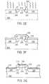
- a typical semiconductor devicea metal oxide semiconductor field effect transistor (MOSFET), includes a polysilicon gate 100 and an insulating gate oxide layer 110 formed over silicon substrate 120 .
- Deep source/drain regions 140(sometimes referred to as heavily doped source and drain regions) and source/drain extension regions 150 (sometimes referred to as lightly doped source and drain regions or LDDs) are formed in substrate 120 , such as by ion implantation.
- oxide spacersare formed abutting the gate 100 to protect the source/drain extension regions from further doping while additional ion implantation is performed to form the deep source/drain regions 140 .
- the source/drain extension 150 and deep source/drain 140are annealed (heated) following ion implantation to obtain the desired material characteristics and to activate the dopants.
- doped regionsare regions containing a higher concentration of p-type or n-type dopants than the substrate.
- silicide regions 170 and 160are typically formed on, over, or within the polysilicon gate 100 and the source/drain regions 140 , respectively.
- Source/drain extension regions 150generally have a lower concentration of dopants compared to deep source/drain regions 140 , although extension regions 150 are increasingly being endowed with dopant concentrations approaching that of the deep source/drain regions 140 .
- Source/drain extension regions 150possess a thickness T 1 smaller than a corresponding thickness T 2 of deep source/drain regions 140 .
- the shallow source/drain extension regions 150are important, for example, in reducing hot carrier injection (HCI) which often occurs in scaled down (e.g., sub-micron) devices and in reducing short channel effects.
- HCIhot carrier injection
- the depth of the source drain extension regionsshould be less than about 700 ⁇ and preferably less than about 500 ⁇ and still more preferably less than 300 ⁇ .
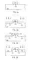
- FIGS. 2A-2GA conventional process for forming the MOSFET shown in FIG. 1 is illustrated in FIGS. 2A-2G. Such a process begins with a substrate 200 upon which is deposited or grown an oxide or other insulating layer. A polysilicon layer or layer of other conducting material is formed over the oxide layer followed by patterning and etching to form gate oxide 205 and polysilicon gate 210 , as shown in FIG. 2 A. Source/drain extension regions 220 are then formed as shown in FIG. 2B, generally by ion implantation with boron, arsenic, or phosphorous ions at energy levels in the range of 1-100 keV. Some processes perform an anneal step following this step to activate doped extension regions 220 .
- spacers 230are formed abutting the gate 210 to protect the underlying source/drain extension regions from subsequent implantation used to form the deep source/drain regions 240 .
- the spacersare typically formed by depositing an oxide layer over the entire wafer, including the substrate and gate, by chemical vapor deposition (CVD) or other well-known method followed by anisotropic etching of the oxide to form the spacers 230 , as shown in FIG. 2 C.
- FIG. 2Eshows an anneal (heating) step, wherein the curved lines represent heating of the structure. Annealing reforms the substrate lattice structure and electrically activates the doped regions 220 and 240 . Annealing typically is done at temperatures above 900° C. and is often performed at temperatures above 1000° C. This annealing is rapidly performed, typically lasting for only about 1-60 seconds depending on the particular temperatures used and objects to be achieved, as known to those skilled in the art.
- a metal layer 250is deposited over the source/drain regions 240 , the gate structure 210 , and sidewall spacers 230 .
- the metal layer 250can be deposited by a PVD method such as sputtering or evaporation, or a CVD method; and is deposited to a thickness of about 100 ⁇ to about 500 ⁇ .
- the deposited metal layer 250is subsequently annealed in a rapid thermal anneal step to form metal silicide contacts 260 and 270 , as shown in FIG. 2 G.
- Nickel silicidefor example, is formed by annealing for about 15 to 120 seconds at between 350° C. to 700° C.
- the thickness of the silicide 260 on the polysilicon gate 210affects the gate's resistance and, therefore, the device's speed. Typically, device performance improves as the gate silicide 260 is made thicker. However, accompanying a thicker gate silicide layer 260 is thicker silicide formation on the source/drain regions 240 , which can lead to detrimental effects on a device's performance. In addition to the silicide layer 270 that forms on the source/drain regions 240 , some silicide forms within the source/drain regions 240 and in the source/drain extensions 220 . The presence of silicide in the source/drain regions 240 and the extension regions 220 can contribute to unwanted short channel effects, such as junction leakage.
- More silicideis likely to be formed in the source/drain regions 240 and the extension regions 220 as the thickness of the desirable silicide layer 270 is increased.
- the device's performanceis also affected by the thickness of the source/drain regions 240 and extension regions 220 .
- the thicknesses of these regions 220 and 240are reduced to improve a device's performance, the amount of excess silicide formation in these regions 220 needed to adversely affect the device (by creating junction leakage) is also reduced.
- embodiments of the present inventionprovide a method for forming silicide contacts with two separate metal deposition steps and accompanying silicide formation steps. According to this method, a metal silicide layer is formed over particular regions of a substrate and then selectively removed from some of those regions. A second metal silicide layer is subsequently formed over the particular regions of the substrate and used as metal silicide contacts for the device.
- One aspect of the present inventionrelates to a semiconductor device that includes a substrate with a polysilicon gate and source/drain regions formed on top.
- a silicide contactis included on the polysilicon gate that is about 5 to 8 times thicker than the silicide contacts on the source/drain regions.
- Another aspect of the present inventionrelates to a method of manufacturing silicide contacts on a semiconductor device that includes forming a gate on a semiconductor substrate, forming at least one source/drain extension region on the substrate, annealing a first deposited metal layer to form metal silicide, removing the metal silicide over the source/drain extension regions while removing only a portion of the silicide over the polysilicon gate, and annealing a second deposited metal layer to form silicide contacts on both the polysilicon gate and the source/drain extension regions.
- One further aspect of the present inventionrelates to a method for forming silicide contacts on a polysilicon gate and source/drain regions that includes the steps of forming silicide on the gate and source/drain regions by annealing a first metal layer, removing a portion of the silicide on the gate and removing substantially all the silicide on the source/drain regions, and then forming the silicide contacts on the gate and source/drain regions by annealing a second metal layer.
- semiconductor devicesas used herein, are not limited to the specifically disclosed embodiments.
- Semiconductor devicesinclude a wide variety of electronic devices including transistors, capacitors, microprocessors, random access memories, etc. In general, semiconductor devices refer to any electrical device comprising semiconductors.
- FIG. 1shows a conventional MOSFET semiconductor device.
- FIGS. 2A-2Gare cross sectional views showing various stages in the formation of the semiconductor device depicted in FIG. 1 .
- FIGS. 3A-3Mare cross-sectional views showing various stages in the formation of the semiconductor device in accord with a first aspect of the invention.
- FIG. 4is a block diagram of a method in accord with the first aspect of the invention.
- the present inventionaddresses and solves problems encountered by conventional methods of forming metal silicide contacts in polysilicon gates, in source/drain regions and in shallow source/drain extension regions.
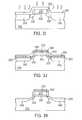
- Substrate 300in FIG. 3A, is doped with an impurity (eg., an n-type impurity), a gate oxide 305 and polysilicon gate 310 are formed, and, as shown in FIG. 3B, source/drain extension regions 320 are formed using the gate 310 as a mask by implanting another type of impurity (e.g., p-type impurity) at an energy level between about 1-10 keV with a dose between about 1 ⁇ 10 14 to 2 ⁇ 10 15 cm ⁇ 2 , such as by ion implantation.
- an impuritye.g., an n-type impurity
- a gate oxide 305 and polysilicon gate 310are formed, and, as shown in FIG. 3B, source/drain extension regions 320 are formed using the gate 310 as a mask by implanting another type of impurity (e.g., p-type impurity) at an energy level between about 1-10 keV with a dose between about 1 ⁇ 10 14 to
- Spacers 330are formed abutting the gate 310 , as illustrated in FIG. 3 C.
- the spacers 330are comprised of any suitable dielectric material such as silicon dioxide, silicon nitride, or silicon oxynitride.
- the sidewall spacers 330are removed from the structure, as shown in FIG. 3F, typically by etching.
- the spacers 330are etched-off by a wet clean method with the wet etch chemistry varying based on the material of the spacers 330 .
- phosphoric acidis typically used and for oxide spacers, HF diluted with water is conventionally used.
- the etched-off sidewall spacers 330are replaced with thinner sidewall spacers 345 , as illustrated in FIG. 3G, that range in thickness freon about 10 ⁇ to about 200 ⁇ .
- the spacers 345can be formed in the conventional manner, described earlier, by performing CVD of an oxide, or other dielectric, layer followed by an anisotropic etching step.
- a layer of metal 350which is preferably Ni, is deposited over the surface of the substrate 300 , gate 310 , spacers 345 and source/drain regions 320 and 340 . While other metal layers such as titanium and cobalt can also be used, the following description assumes the use of a nickel layer 350 .
- the nickel layer 350 depositioncan be effected in any conventional manner.
- the structureis then annealed, in FIG. 3I, at a temperature between a range of 280° C.-700° C., wherein the lower limit is the temperature at which Ni begins to react with silicon. More preferably, annealing is conducted at a temperature between about 400° C.-600° C. The anneal duration varies in accord with the anneal temperature, among other factors, and lasts for about 5-30 seconds, although a range of 1-60 seconds is acceptable.
- the annealing processforms NiSi 360 over source/drain regions 320 and 340 to a depth between about 200-400 ⁇ , forcing the dopant into the source/drain regions 320 and 340 and causing a dopant pile up 325 (i.e., increased dopant concentration) at the NiSi/Si interface region, as shown in FIG. 3 J.
- NiSiis formed on the gate 310 at the same rate as in the active regions 320 and 340 .
- the rate of NiSi formation on the gate 310is increased due to nickel reacting with both the side surfaces and the top surface of the gate 310 .
- tie NiSi layer 365has a thickness of between about 600 ⁇ and about 1200 ⁇ .
- any unreacted nickel 350 and the NiSi 360 over the source/drain regions 320 and 340is removed, as shown in FIG. 3 K.
- the NiSi 360may be advantageously removed, for example, by etching using an appropriate etchant, such as APM (ammonium hydroxide-peroxide mix), leaving behind a thinner portion of the source/drain extension region comprising Si with the dopant pile up 325 at the NiSi/Si interface region.
- APMammonium hydroxide-peroxide mix
- a second metal layer 380preferably comprising nickel, is deposited over the regions of the device.
- This second metal layer 380can be deposited using similar methods as earlier but is deposited with a thickness of between approximately 20 ⁇ and approximately 100 ⁇ .
- an annealingis performed to form silicide layers 385 and 390 , as shown in FIG. 3 M.
- the NiSi layer 385 aver the gate 310forms to a thickness of between about 150 ⁇ and about 600 ⁇ and the NiSi layers 390 over the source/drain regions 320 and 340 form to a thickness of between about 50 ⁇ and about 206 ⁇ .
- any unreacted metal from layer 380is etched away, in a conventional manner that is selective to the unreacted nickel relative to the nickel silicide, to form the device depicted in FIG. 3 M.
- the relatively thick silicide gate contact 385is formed by the combination of the two metal deposition steps and accompanying silicidation steps.
- the relatively thin silicide source/drain contactsare formed only by the latter metal deposition and silicidation steps.
- the silicide gate contact 385has a thickness that is about 5 to 8 times the thickness of the silicide source/drain contacts.
- a semiconductor devicehas been shown, according to the present inventive methodology, that has a gate silicide contact of sufficient thickness to provide desired performance benefits but with thinner source/drain silicide contacts that do not contribute to the formation of undesirable silicide in the source/drain regions and source/drain extension regions that can increase the likelihood of junction leakage and short channel effects.
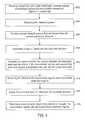
- step 402impurity regions, the polysilicon gate and the sidewall spacers are formed on a substrate.
- step 404the sidewall spacers are removed.
- a second pair of thinner sidewall spacersare then formed, in step 406 , on the remaining structure.
- step 408a metal layer is deposited and is then annealed in step 410 at a temperature sufficient to effect a silicidation reaction between the deposited metal and the silicon in the source/drain regions and the source/drain extension regions of the silicon substrate to form a dopant pile up at the silicide/Si substrate interface.
- the deposited metalalso reacts with the silicon in the polysilicon gate.
- the silicideis etched away in step 412 , leaving behind a portion of the source/drain extension region comprising Si with the dopant pile up, thereby forming a shallow junction. Also left behind is a layer of silicide formed on the polysilicon gate.
- a second layer of metalis deposited over the structure and annealed, in step 416 , to form silicide contacts; the silicide contacts over the source drain regions being thinner than the silicide contact over the polysilicon gate.
- the present inventionachieves the technological advantage of enabling both the formation of reliable gate silicide contacts and the formation of silicide contacts within ultra-shallow source/drain junctions to meet the increasing demands for high density and miniaturization.
- the present inventionis applicable to the manufacture of various types of semiconductor devices, particularly semiconductor devices having a design rule of less than about 0.18 microns.
Landscapes
- Engineering & Computer Science (AREA)
- Physics & Mathematics (AREA)
- Condensed Matter Physics & Semiconductors (AREA)
- General Physics & Mathematics (AREA)
- Manufacturing & Machinery (AREA)
- Computer Hardware Design (AREA)
- Microelectronics & Electronic Packaging (AREA)
- Power Engineering (AREA)
- Electrodes Of Semiconductors (AREA)
- Insulated Gate Type Field-Effect Transistor (AREA)
Abstract
Description
Claims (18)
Priority Applications (1)
| Application Number | Priority Date | Filing Date | Title |
|---|---|---|---|
| US09/679,370US6451693B1 (en) | 2000-10-05 | 2000-10-05 | Double silicide formation in polysicon gate without silicide in source/drain extensions |
Applications Claiming Priority (1)
| Application Number | Priority Date | Filing Date | Title |
|---|---|---|---|
| US09/679,370US6451693B1 (en) | 2000-10-05 | 2000-10-05 | Double silicide formation in polysicon gate without silicide in source/drain extensions |
Publications (1)
| Publication Number | Publication Date |
|---|---|
| US6451693B1true US6451693B1 (en) | 2002-09-17 |
Family
ID=24726643
Family Applications (1)
| Application Number | Title | Priority Date | Filing Date |
|---|---|---|---|
| US09/679,370Expired - LifetimeUS6451693B1 (en) | 2000-10-05 | 2000-10-05 | Double silicide formation in polysicon gate without silicide in source/drain extensions |
Country Status (1)
| Country | Link |
|---|---|
| US (1) | US6451693B1 (en) |
Cited By (28)
| Publication number | Priority date | Publication date | Assignee | Title |
|---|---|---|---|---|
| US20030183881A1 (en)* | 2002-03-28 | 2003-10-02 | Lee Young-Ki | Methods of forming silicide layers on source/drain regions of MOS transistors and MOS transistors so formed |
| US20040077158A1 (en)* | 2002-10-17 | 2004-04-22 | Hyeon-Ill Um | Method of manufacturing semiconductor device through salicide process |
| US6855989B1 (en) | 2003-10-01 | 2005-02-15 | Advanced Micro Devices, Inc. | Damascene finfet gate with selective metal interdiffusion |
| US20050067745A1 (en)* | 2003-09-30 | 2005-03-31 | Giewont Kenneth John | Method and apparatus for deposition & formation of metal silicides |
| WO2005062387A1 (en)* | 2003-12-03 | 2005-07-07 | Advanced Micro Devices, Inc. | Formation of abrupt junctions in devices by using silicide growth dopant snowplow effect |
| US6936528B2 (en) | 2002-10-17 | 2005-08-30 | Samsung Electronics Co., Ltd. | Method of forming cobalt silicide film and method of manufacturing semiconductor device having cobalt silicide film |
| US6936882B1 (en)* | 2003-07-08 | 2005-08-30 | Advanced Micro Devices, Inc. | Selective silicidation of gates in semiconductor devices to achieve multiple threshold voltages |
| US20060040438A1 (en)* | 2004-08-17 | 2006-02-23 | Jiong-Ping Lu | Method for improving the thermal stability of silicide |
| US20060211213A1 (en)* | 2005-03-15 | 2006-09-21 | Kim Tae K | Method of manufacturing semiconductor device having step gate |
| US20060252191A1 (en)* | 2005-05-03 | 2006-11-09 | Advanced Micro Devices, Inc. | Methodology for deposition of doped SEG for raised source/drain regions |
| US20060281271A1 (en)* | 2005-06-13 | 2006-12-14 | Advanced Micro Devices, Inc. | Method of forming a semiconductor device having an epitaxial layer and device thereof |
| US20070059912A1 (en)* | 2005-09-15 | 2007-03-15 | Jong-Ho Yun | Method of forming metal silicide layer and related method of fabricating semiconductor devices |
| US20070117376A1 (en)* | 2005-11-24 | 2007-05-24 | Dongbuanam Semiconductor Inc. | Method for fabricating a semiconductor device |
| US7241700B1 (en)* | 2004-10-20 | 2007-07-10 | Advanced Micro Devices, Inc. | Methods for post offset spacer clean for improved selective epitaxy silicon growth |
| US20070178683A1 (en)* | 2006-02-02 | 2007-08-02 | Texas Instruments, Incorporated | Semiconductive device fabricated using a two step approach to silicide a gate and source/drains |
| US7262104B1 (en) | 2004-06-02 | 2007-08-28 | Advanced Micro Devices, Inc. | Selective channel implantation for forming semiconductor devices with different threshold voltages |
| US20070278583A1 (en)* | 2006-06-01 | 2007-12-06 | International Business Machines Corporation | Gate stress engineering for mosfet |
| US20080044991A1 (en)* | 2006-08-21 | 2008-02-21 | Kabushiki Kaisha Toshiba | Semiconductor device and method of fabricating the same |
| US20080156265A1 (en)* | 2005-10-03 | 2008-07-03 | International Business Machines Corporation | Method and apparatus for forming nickel silicide with low defect density in fet devices |
| US7402485B1 (en) | 2004-10-20 | 2008-07-22 | Advanced Micro Devices, Inc. | Method of forming a semiconductor device |
| US7402207B1 (en) | 2004-05-05 | 2008-07-22 | Advanced Micro Devices, Inc. | Method and apparatus for controlling the thickness of a selective epitaxial growth layer |
| US20080242094A1 (en)* | 2007-03-30 | 2008-10-02 | Trivedi Vishal P | Method of making a semiconductor structure utilizing spacer removal and semiconductor structure |
| US7456062B1 (en) | 2004-10-20 | 2008-11-25 | Advanced Micro Devices, Inc. | Method of forming a semiconductor device |
| US20090004851A1 (en)* | 2007-06-29 | 2009-01-01 | Taiwan Semiconductor Manufacturing Co., Ltd. | Salicidation process using electroless plating to deposit metal and introduce dopant impurities |
| US20090057776A1 (en)* | 2007-04-27 | 2009-03-05 | Texas Instruments Incorporated | Method of forming fully silicided nmos and pmos semiconductor devices having independent polysilicon gate thicknesses, and related device |
| US7553732B1 (en) | 2005-06-13 | 2009-06-30 | Advanced Micro Devices, Inc. | Integration scheme for constrained SEG growth on poly during raised S/D processing |
| US7572705B1 (en) | 2005-09-21 | 2009-08-11 | Advanced Micro Devices, Inc. | Semiconductor device and method of manufacturing a semiconductor device |
| CN102832126A (en)* | 2011-06-13 | 2012-12-19 | 中国科学院微电子研究所 | Semiconductor structure and manufacturing method thereof |
Citations (13)
| Publication number | Priority date | Publication date | Assignee | Title |
|---|---|---|---|---|
| US4877755A (en)* | 1988-05-31 | 1989-10-31 | Texas Instruments Incorporated | Method of forming silicides having different thicknesses |
| US5322809A (en)* | 1993-05-11 | 1994-06-21 | Texas Instruments Incorporated | Self-aligned silicide process |
| US5723377A (en)* | 1995-06-13 | 1998-03-03 | Nec Corporation | Process for manufacturing a semiconductor device including a silicidation step |
| US5814537A (en)* | 1996-12-18 | 1998-09-29 | Sharp Microelectronics Technology,Inc. | Method of forming transistor electrodes from directionally deposited silicide |
| US5904533A (en)* | 1997-02-04 | 1999-05-18 | Winbond Electronics Corp. | Metal salicide-CMP-metal salicide semiconductor process |
| US5970380A (en)* | 1997-05-20 | 1999-10-19 | Samsung Electronics Co., Ltd. | Methods of forming semiconductor switching devices having silicide regions therein |
| US5972785A (en)* | 1996-10-21 | 1999-10-26 | Nec Corporation | Method for manufacturing a semiconductor device having a refractory metal silicide layer |
| US6060387A (en)* | 1995-11-20 | 2000-05-09 | Compaq Computer Corporation | Transistor fabrication process in which a contact metallization is formed with different silicide thickness over gate interconnect material and transistor source/drain regions |
| US6063681A (en)* | 1998-01-13 | 2000-05-16 | Lg Semicon Co., Ltd. | Silicide formation using two metalizations |
| US6110811A (en)* | 1998-06-11 | 2000-08-29 | Chartered Semiconductor Manufacturing Ltd. | Selective CVD TiSi2 deposition with TiSi2 liner |
| US6140232A (en)* | 1999-08-31 | 2000-10-31 | United Microelectronics Corp. | Method for reducing silicide resistance |
| US6156649A (en)* | 1998-04-14 | 2000-12-05 | Advanced Micro Devices, Inc. | Method of forming uniform sheet resistivity salicide |
| US6211016B1 (en)* | 1998-03-23 | 2001-04-03 | Texas Instruments-Acer Incorporated | Method for forming high density nonvolatile memories with high capacitive-coupling ratio |
- 2000
- 2000-10-05USUS09/679,370patent/US6451693B1/ennot_activeExpired - Lifetime
Patent Citations (13)
| Publication number | Priority date | Publication date | Assignee | Title |
|---|---|---|---|---|
| US4877755A (en)* | 1988-05-31 | 1989-10-31 | Texas Instruments Incorporated | Method of forming silicides having different thicknesses |
| US5322809A (en)* | 1993-05-11 | 1994-06-21 | Texas Instruments Incorporated | Self-aligned silicide process |
| US5723377A (en)* | 1995-06-13 | 1998-03-03 | Nec Corporation | Process for manufacturing a semiconductor device including a silicidation step |
| US6060387A (en)* | 1995-11-20 | 2000-05-09 | Compaq Computer Corporation | Transistor fabrication process in which a contact metallization is formed with different silicide thickness over gate interconnect material and transistor source/drain regions |
| US5972785A (en)* | 1996-10-21 | 1999-10-26 | Nec Corporation | Method for manufacturing a semiconductor device having a refractory metal silicide layer |
| US5814537A (en)* | 1996-12-18 | 1998-09-29 | Sharp Microelectronics Technology,Inc. | Method of forming transistor electrodes from directionally deposited silicide |
| US5904533A (en)* | 1997-02-04 | 1999-05-18 | Winbond Electronics Corp. | Metal salicide-CMP-metal salicide semiconductor process |
| US5970380A (en)* | 1997-05-20 | 1999-10-19 | Samsung Electronics Co., Ltd. | Methods of forming semiconductor switching devices having silicide regions therein |
| US6063681A (en)* | 1998-01-13 | 2000-05-16 | Lg Semicon Co., Ltd. | Silicide formation using two metalizations |
| US6211016B1 (en)* | 1998-03-23 | 2001-04-03 | Texas Instruments-Acer Incorporated | Method for forming high density nonvolatile memories with high capacitive-coupling ratio |
| US6156649A (en)* | 1998-04-14 | 2000-12-05 | Advanced Micro Devices, Inc. | Method of forming uniform sheet resistivity salicide |
| US6110811A (en)* | 1998-06-11 | 2000-08-29 | Chartered Semiconductor Manufacturing Ltd. | Selective CVD TiSi2 deposition with TiSi2 liner |
| US6140232A (en)* | 1999-08-31 | 2000-10-31 | United Microelectronics Corp. | Method for reducing silicide resistance |
Cited By (48)
| Publication number | Priority date | Publication date | Assignee | Title |
|---|---|---|---|---|
| US7211515B2 (en)* | 2002-03-28 | 2007-05-01 | Samsung Electronics Co., Ltd. | Methods of forming silicide layers on source/drain regions of MOS transistors |
| US20030183881A1 (en)* | 2002-03-28 | 2003-10-02 | Lee Young-Ki | Methods of forming silicide layers on source/drain regions of MOS transistors and MOS transistors so formed |
| US20070170501A1 (en)* | 2002-03-28 | 2007-07-26 | Lee Young-Ki | MOS Transistors Including Silicide Layers on Source/Drain Regions |
| US20050196960A1 (en)* | 2002-10-17 | 2005-09-08 | Kyeong-Mo Koo | Method of forming metal silicide film and method of manufacturing semiconductor device having metal silicide film |
| US20040077158A1 (en)* | 2002-10-17 | 2004-04-22 | Hyeon-Ill Um | Method of manufacturing semiconductor device through salicide process |
| US6936528B2 (en) | 2002-10-17 | 2005-08-30 | Samsung Electronics Co., Ltd. | Method of forming cobalt silicide film and method of manufacturing semiconductor device having cobalt silicide film |
| US6936882B1 (en)* | 2003-07-08 | 2005-08-30 | Advanced Micro Devices, Inc. | Selective silicidation of gates in semiconductor devices to achieve multiple threshold voltages |
| US20050067745A1 (en)* | 2003-09-30 | 2005-03-31 | Giewont Kenneth John | Method and apparatus for deposition & formation of metal silicides |
| US20070087541A1 (en)* | 2003-09-30 | 2007-04-19 | Giewont Kenneth J | Method and apparatus for deposition & formation of metal silicides |
| US6855989B1 (en) | 2003-10-01 | 2005-02-15 | Advanced Micro Devices, Inc. | Damascene finfet gate with selective metal interdiffusion |
| GB2425404B (en)* | 2003-12-03 | 2007-05-16 | Advanced Micro Devices Inc | Formation of abrupt junctions in devices by using silicide growth dopant snowplow effect |
| US20060211245A1 (en)* | 2003-12-03 | 2006-09-21 | Advanced Micro Devices, Inc. | Formation of abrupt junctions in devices by using silicide growth dopant snowplow effect |
| WO2005062387A1 (en)* | 2003-12-03 | 2005-07-07 | Advanced Micro Devices, Inc. | Formation of abrupt junctions in devices by using silicide growth dopant snowplow effect |
| GB2425404A (en)* | 2003-12-03 | 2006-10-25 | Advanced Micro Devices Inc | Formation of abrupt junctions in devices by using silicide growth dopant snowplow effect |
| US7306998B2 (en) | 2003-12-03 | 2007-12-11 | Advanced Micro Devices, Inc. | Formation of abrupt junctions in devices by using silicide growth dopant snowplow effect |
| US7402207B1 (en) | 2004-05-05 | 2008-07-22 | Advanced Micro Devices, Inc. | Method and apparatus for controlling the thickness of a selective epitaxial growth layer |
| US7262104B1 (en) | 2004-06-02 | 2007-08-28 | Advanced Micro Devices, Inc. | Selective channel implantation for forming semiconductor devices with different threshold voltages |
| US20060040438A1 (en)* | 2004-08-17 | 2006-02-23 | Jiong-Ping Lu | Method for improving the thermal stability of silicide |
| US20110151637A1 (en)* | 2004-08-17 | 2011-06-23 | Texas Instruments Incorporated | Method for Improving the Thermal Stability of Silicide |
| US7456062B1 (en) | 2004-10-20 | 2008-11-25 | Advanced Micro Devices, Inc. | Method of forming a semiconductor device |
| US7241700B1 (en)* | 2004-10-20 | 2007-07-10 | Advanced Micro Devices, Inc. | Methods for post offset spacer clean for improved selective epitaxy silicon growth |
| US7402485B1 (en) | 2004-10-20 | 2008-07-22 | Advanced Micro Devices, Inc. | Method of forming a semiconductor device |
| US20060211213A1 (en)* | 2005-03-15 | 2006-09-21 | Kim Tae K | Method of manufacturing semiconductor device having step gate |
| US7148108B2 (en)* | 2005-03-15 | 2006-12-12 | Hynix Semiconductor Inc. | Method of manufacturing semiconductor device having step gate |
| US20060252191A1 (en)* | 2005-05-03 | 2006-11-09 | Advanced Micro Devices, Inc. | Methodology for deposition of doped SEG for raised source/drain regions |
| US20090236664A1 (en)* | 2005-06-13 | 2009-09-24 | Advanced Micro Devices, Inc. | Integration scheme for constrained seg growth on poly during raised s/d processing |
| US20060281271A1 (en)* | 2005-06-13 | 2006-12-14 | Advanced Micro Devices, Inc. | Method of forming a semiconductor device having an epitaxial layer and device thereof |
| US7553732B1 (en) | 2005-06-13 | 2009-06-30 | Advanced Micro Devices, Inc. | Integration scheme for constrained SEG growth on poly during raised S/D processing |
| US20070059912A1 (en)* | 2005-09-15 | 2007-03-15 | Jong-Ho Yun | Method of forming metal silicide layer and related method of fabricating semiconductor devices |
| US7572705B1 (en) | 2005-09-21 | 2009-08-11 | Advanced Micro Devices, Inc. | Semiconductor device and method of manufacturing a semiconductor device |
| US7910996B2 (en) | 2005-09-21 | 2011-03-22 | Globalfoundries Inc. | Semiconductor device and method of manufacturing a semiconductor device |
| US8298385B2 (en) | 2005-10-03 | 2012-10-30 | International Business Machines Corporation | Method and apparatus for forming nickel silicide with low defect density in FET devices |
| US20080156265A1 (en)* | 2005-10-03 | 2008-07-03 | International Business Machines Corporation | Method and apparatus for forming nickel silicide with low defect density in fet devices |
| US7759741B2 (en)* | 2005-10-03 | 2010-07-20 | International Business Machines Corporation | Method and apparatus for forming nickel silicide with low defect density in FET devices |
| US20080164540A1 (en)* | 2005-10-03 | 2008-07-10 | International Business Machines Corporation | Method and apparatus for forming nickel silicide with low defect density in fet devices |
| US20070117376A1 (en)* | 2005-11-24 | 2007-05-24 | Dongbuanam Semiconductor Inc. | Method for fabricating a semiconductor device |
| US20070178683A1 (en)* | 2006-02-02 | 2007-08-02 | Texas Instruments, Incorporated | Semiconductive device fabricated using a two step approach to silicide a gate and source/drains |
| US7595233B2 (en) | 2006-06-01 | 2009-09-29 | International Business Machines Corporation | Gate stress engineering for MOSFET |
| US20070278583A1 (en)* | 2006-06-01 | 2007-12-06 | International Business Machines Corporation | Gate stress engineering for mosfet |
| US7723231B2 (en)* | 2006-08-21 | 2010-05-25 | Kabushiki Kaisha Toshiba | Semiconductor device and method of fabricating the same |
| US20080044991A1 (en)* | 2006-08-21 | 2008-02-21 | Kabushiki Kaisha Toshiba | Semiconductor device and method of fabricating the same |
| US7713801B2 (en)* | 2007-03-30 | 2010-05-11 | Trivedi Vishal P | Method of making a semiconductor structure utilizing spacer removal and semiconductor structure |
| US20080242094A1 (en)* | 2007-03-30 | 2008-10-02 | Trivedi Vishal P | Method of making a semiconductor structure utilizing spacer removal and semiconductor structure |
| US20090057776A1 (en)* | 2007-04-27 | 2009-03-05 | Texas Instruments Incorporated | Method of forming fully silicided nmos and pmos semiconductor devices having independent polysilicon gate thicknesses, and related device |
| US8574980B2 (en)* | 2007-04-27 | 2013-11-05 | Texas Instruments Incorporated | Method of forming fully silicided NMOS and PMOS semiconductor devices having independent polysilicon gate thicknesses, and related device |
| US20090004851A1 (en)* | 2007-06-29 | 2009-01-01 | Taiwan Semiconductor Manufacturing Co., Ltd. | Salicidation process using electroless plating to deposit metal and introduce dopant impurities |
| CN102832126A (en)* | 2011-06-13 | 2012-12-19 | 中国科学院微电子研究所 | Semiconductor structure and manufacturing method thereof |
| US8809134B2 (en)* | 2011-06-13 | 2014-08-19 | The Institute of Microelectronics Chinese Academy of Science | Semiconductor structure and method for manufacturing the same |
Similar Documents
| Publication | Publication Date | Title |
|---|---|---|
| US6451693B1 (en) | Double silicide formation in polysicon gate without silicide in source/drain extensions | |
| US6562718B1 (en) | Process for forming fully silicided gates | |
| KR0135163B1 (en) | Manufacturing method of mos transistor with shallow | |
| KR100271948B1 (en) | Method for forming self-align silicide in semiconductor device | |
| US7396767B2 (en) | Semiconductor structure including silicide regions and method of making same | |
| US6255703B1 (en) | Device with lower LDD resistance | |
| US6630721B1 (en) | Polysilicon sidewall with silicide formation to produce high performance MOSFETS | |
| US6015752A (en) | Elevated salicide technology | |
| US20020137297A1 (en) | Method of manufacturing semiconductor device | |
| US6242776B1 (en) | Device improvement by lowering LDD resistance with new silicide process | |
| US6534402B1 (en) | Method of fabricating self-aligned silicide | |
| US6784506B2 (en) | Silicide process using high K-dielectrics | |
| US6271133B1 (en) | Optimized Co/Ti-salicide scheme for shallow junction deep sub-micron device fabrication | |
| US6277721B1 (en) | Salicide formation process | |
| US6767831B1 (en) | Method for forming cobalt salicides | |
| US6156615A (en) | Method for decreasing the contact resistance of silicide contacts by retrograde implantation of source/drain regions | |
| US7189644B2 (en) | CMOS device integration for low external resistance | |
| US7320938B2 (en) | Method for reducing dendrite formation in nickel silicon salicide processes | |
| US6740570B2 (en) | Method for forming a self-aligned silicide of a metal oxide semiconductor | |
| US20010011756A1 (en) | Method for forming shallow source/drain extension for mos transistor | |
| US20060003534A1 (en) | Salicide process using bi-metal layer and method of fabricating semiconductor device using the same | |
| US6376343B1 (en) | Reduction of metal silicide/silicon interface roughness by dopant implantation processing | |
| US6727558B1 (en) | Channel isolation using dielectric isolation structures | |
| US6586331B2 (en) | Low sheet resistance of titanium salicide process | |
| US6777300B2 (en) | Method to improve silicide formation on polysilicon |
Legal Events
| Date | Code | Title | Description |
|---|---|---|---|
| AS | Assignment | Owner name:ADVANCED MICRO DEVICES, INC., CALIFORNIA Free format text:ASSIGNMENT OF ASSIGNORS INTEREST;ASSIGNORS:WOO, CHRISTY MEI-CHU;KLUTH, GEORGE JONATHAN;ZIANG, QI;REEL/FRAME:011198/0636 Effective date:20000929 | |
| STCF | Information on status: patent grant | Free format text:PATENTED CASE | |
| CC | Certificate of correction | ||
| FPAY | Fee payment | Year of fee payment:4 | |
| AS | Assignment | Owner name:GLOBALFOUNDRIES INC., CAYMAN ISLANDS Free format text:AFFIRMATION OF PATENT ASSIGNMENT;ASSIGNOR:ADVANCED MICRO DEVICES, INC.;REEL/FRAME:023119/0083 Effective date:20090630 | |
| FPAY | Fee payment | Year of fee payment:8 | |
| FPAY | Fee payment | Year of fee payment:12 | |
| AS | Assignment | Owner name:WILMINGTON TRUST, NATIONAL ASSOCIATION, DELAWARE Free format text:SECURITY AGREEMENT;ASSIGNOR:GLOBALFOUNDRIES INC.;REEL/FRAME:049490/0001 Effective date:20181127 | |
| AS | Assignment | Owner name:GLOBALFOUNDRIES U.S. INC., CALIFORNIA Free format text:ASSIGNMENT OF ASSIGNORS INTEREST;ASSIGNOR:GLOBALFOUNDRIES INC.;REEL/FRAME:054633/0001 Effective date:20201022 | |
| AS | Assignment | Owner name:GLOBALFOUNDRIES INC., CAYMAN ISLANDS Free format text:RELEASE BY SECURED PARTY;ASSIGNOR:WILMINGTON TRUST, NATIONAL ASSOCIATION;REEL/FRAME:054636/0001 Effective date:20201117 | |
| AS | Assignment | Owner name:GLOBALFOUNDRIES U.S. INC., NEW YORK Free format text:RELEASE BY SECURED PARTY;ASSIGNOR:WILMINGTON TRUST, NATIONAL ASSOCIATION;REEL/FRAME:056987/0001 Effective date:20201117 |