US6451685B1 - Method for multilevel copper interconnects for ultra large scale integration - Google Patents
Method for multilevel copper interconnects for ultra large scale integrationDownload PDFInfo
- Publication number
- US6451685B1 US6451685B1US09/777,816US77781601AUS6451685B1US 6451685 B1US6451685 B1US 6451685B1US 77781601 AUS77781601 AUS 77781601AUS 6451685 B1US6451685 B1US 6451685B1
- Authority
- US
- United States
- Prior art keywords
- metal
- metal oxide
- layer
- copper
- portions
- Prior art date
- Legal status (The legal status is an assumption and is not a legal conclusion. Google has not performed a legal analysis and makes no representation as to the accuracy of the status listed.)
- Expired - Lifetime
Links
Images


Classifications
- H—ELECTRICITY
- H01—ELECTRIC ELEMENTS
- H01L—SEMICONDUCTOR DEVICES NOT COVERED BY CLASS H10
- H01L21/00—Processes or apparatus adapted for the manufacture or treatment of semiconductor or solid state devices or of parts thereof
- H01L21/02—Manufacture or treatment of semiconductor devices or of parts thereof
- H01L21/04—Manufacture or treatment of semiconductor devices or of parts thereof the devices having potential barriers, e.g. a PN junction, depletion layer or carrier concentration layer
- H01L21/18—Manufacture or treatment of semiconductor devices or of parts thereof the devices having potential barriers, e.g. a PN junction, depletion layer or carrier concentration layer the devices having semiconductor bodies comprising elements of Group IV of the Periodic Table or AIIIBV compounds with or without impurities, e.g. doping materials
- H01L21/30—Treatment of semiconductor bodies using processes or apparatus not provided for in groups H01L21/20 - H01L21/26
- H01L21/31—Treatment of semiconductor bodies using processes or apparatus not provided for in groups H01L21/20 - H01L21/26 to form insulating layers thereon, e.g. for masking or by using photolithographic techniques; After treatment of these layers; Selection of materials for these layers
- H01L21/3205—Deposition of non-insulating-, e.g. conductive- or resistive-, layers on insulating layers; After-treatment of these layers
- H—ELECTRICITY
- H01—ELECTRIC ELEMENTS
- H01L—SEMICONDUCTOR DEVICES NOT COVERED BY CLASS H10
- H01L21/00—Processes or apparatus adapted for the manufacture or treatment of semiconductor or solid state devices or of parts thereof
- H01L21/70—Manufacture or treatment of devices consisting of a plurality of solid state components formed in or on a common substrate or of parts thereof; Manufacture of integrated circuit devices or of parts thereof
- H01L21/71—Manufacture of specific parts of devices defined in group H01L21/70
- H01L21/768—Applying interconnections to be used for carrying current between separate components within a device comprising conductors and dielectrics
- H01L21/76801—Applying interconnections to be used for carrying current between separate components within a device comprising conductors and dielectrics characterised by the formation and the after-treatment of the dielectrics, e.g. smoothing
- H01L21/76822—Modification of the material of dielectric layers, e.g. grading, after-treatment to improve the stability of the layers, to increase their density etc.
- H01L21/76823—Modification of the material of dielectric layers, e.g. grading, after-treatment to improve the stability of the layers, to increase their density etc. transforming an insulating layer into a conductive layer
- H—ELECTRICITY
- H01—ELECTRIC ELEMENTS
- H01L—SEMICONDUCTOR DEVICES NOT COVERED BY CLASS H10
- H01L21/00—Processes or apparatus adapted for the manufacture or treatment of semiconductor or solid state devices or of parts thereof
- H01L21/70—Manufacture or treatment of devices consisting of a plurality of solid state components formed in or on a common substrate or of parts thereof; Manufacture of integrated circuit devices or of parts thereof
- H01L21/71—Manufacture of specific parts of devices defined in group H01L21/70
- H01L21/768—Applying interconnections to be used for carrying current between separate components within a device comprising conductors and dielectrics
- H01L21/76801—Applying interconnections to be used for carrying current between separate components within a device comprising conductors and dielectrics characterised by the formation and the after-treatment of the dielectrics, e.g. smoothing
- H01L21/76829—Applying interconnections to be used for carrying current between separate components within a device comprising conductors and dielectrics characterised by the formation and the after-treatment of the dielectrics, e.g. smoothing characterised by the formation of thin functional dielectric layers, e.g. dielectric etch-stop, barrier, capping or liner layers
- H—ELECTRICITY
- H01—ELECTRIC ELEMENTS
- H01L—SEMICONDUCTOR DEVICES NOT COVERED BY CLASS H10
- H01L21/00—Processes or apparatus adapted for the manufacture or treatment of semiconductor or solid state devices or of parts thereof
- H01L21/70—Manufacture or treatment of devices consisting of a plurality of solid state components formed in or on a common substrate or of parts thereof; Manufacture of integrated circuit devices or of parts thereof
- H01L21/71—Manufacture of specific parts of devices defined in group H01L21/70
- H01L21/768—Applying interconnections to be used for carrying current between separate components within a device comprising conductors and dielectrics
- H01L21/76838—Applying interconnections to be used for carrying current between separate components within a device comprising conductors and dielectrics characterised by the formation and the after-treatment of the conductors
- H01L21/76877—Filling of holes, grooves or trenches, e.g. vias, with conductive material
- H01L21/76879—Filling of holes, grooves or trenches, e.g. vias, with conductive material by selective deposition of conductive material in the vias, e.g. selective C.V.D. on semiconductor material, plating
Definitions
- the present inventionis related to U.S. patent appication Ser. No. 09/679,159, entitled “Telescope for a Free-Space Wireless Optical Communication System,” U.S. patent application Ser. No. 09/680,165, entitled “Method and Apparatus for Controlling Received Power Levels Within a Free-Space Optical Communication System,” U.S. patent application Ser. No. 09/680,336, entitled “Method and Apparatus for Aligning Telescopes Within a Free-Space Optical Communication System” and U.S. patent application Ser. No. 09/680,812, entitled “Method and Apparatus for Communication Signal Autotracking Within a Free-Space Optical Communication System,” each filed contemporaneously herewith, assigned to the assignee of the present invention and incorporated by reference herein.
- the present inventionrelates to the manufacturing of integrated circuits.
- this inventionrelates to using a thin copper oxide film as a seed layer for building multilevel interconnects structures in integrated circuits.
- interconnect systemsare gradually migrating away from aluminum thin films to copper thin films.
- copperhas more advantages, which are critical for improving integrated circuit performance.
- copperhas a much lower sheet resistivity than aluminum.
- a copper linecan be made narrower and thinner than an aluminum one. Therefore, using a copper line allows for higher integration density.
- narrower and thinner conductive linesdecrease both inter-level and inter-line capacitance, which leads to higher speed and less bleed over for the circuit.
- copperhas a better electromigration resistance than aluminum. Accordingly, as metal lines are made thinner and circuitry becomes more densely packed, copper provides higher reliability when used in ICs.
- the most promising methodappears to be the Damascene process.
- the trenches and viasare formed in blanket dielectrics, and then a metal is deposited into the trenches and holes in one step, which is then followed by chemical mechanical planarization (CMP) to remove the unwanted surface metal.
- CMPchemical mechanical planarization
- a selective copper deposition by electroless plating or chemical vaporization deposition (CVD)offers a “CMP-less” metallization technology.
- multilevel copper interconnectsincluding metal lines and via holes, are fabricated on a wafer.
- a thin seed layer of copper oxideis deposited over the wafer.
- the exposed copper oxideis converted to copper using an ultra-violet photo reduction method.
- a copper filmis deposited using electroless plating or chemical vaporization deposition (CVD) and a planar surface is thereby provided.
- via holesare fabricated using conventional methods such as via hole lithography, and a second layer of copper oxide is deposited in a manner similar to the first. As with the first copper layer, a planar surface is provided for subsequent layers.
- multilevel interconnect structures with as many metal layers as desiredcan be manufactured by repeating the process, and without the need for CMP.
- One key advantage of using copper oxide in lieu of copper as the seed layeris the potentially high manufacturing yield in ICs. If a pure copper seed layer is used, a native copper oxide may form on the surface of the wafer depending upon how long the wafer is exposed to the air. This makes reproducibility an issue unless an additional step of removing the copper oxide is performed.
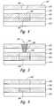
- FIGS. 1-5are cross-sectional views illustrating the exemplary method for manufacturing multilevel metal interconnects for ultra large-scale integration.
- FIG. 6is a cross-sectional view of an alternate embodiment of the invention.
- FIGS. 1-5show a number of cross-sectional views, which taken collectively and sequentially, illustrate an exemplary method of making multilevel interconnects for ULSI.
- the methodbegins with a semiconductor wafer 210 .
- the semiconductor wafer 210may be at any stage of fabrication.
- a thin layer of a copper oxide 220is deposited on the surface of the semiconductor wafer 210 . While copper and copper oxide are disclosed herein to fabricate multilevel interconnects, it can be appreciated that other metals and their oxides, such as platinum and palladium, for example, are also well suited for use in the disclosed method.
- various techniquescan be used for depositing the copper oxide layer 220 , including, but not limited to, CVD, ionized-magnetron sputtering technique, DC magnetron self-sputtering technique, plasma evaporation, plasma-enhance CVD, metalorganic microwave plasma CVD, CVD from copper dipivaloymethanate, and pulsed laser deposition.
- a metal line pattern 215is defined by standard optical lithography using a first photoresist layer 230 .
- the thickness of the photoresist layer 230is carefully chosen to match that of the metal line 215 .
- the exposed copper oxide 220is then converted to a copper layer 240 in-situ by UV photo-reduction according to conventional or hereinafter developed processes, including, for example, the method described in co-pending and co-assigned patent application entitled “CONDUCTIVE MATERIAL PATTERNING METHODS,” Micron Docket No. 99-0671, which is incorporated herein by reference.
- a copper film 250is deposited selectively to a desired thickness by either selective CVD or electroless plating. After these steps, a planar surface 255 is provided for subsequent steps without CMP.
- a via hole 280may also be fabricated.
- a second seed layer of copper oxide 260is deposited over the first photoresist layer 230 and the copper layer 250 in a manner similar to depositing the first layer of copper oxide 220 , as discussed above.
- via hole lithographyis performed using a photo resist layer 270 having a thickness corresponding to the length of a via 280 .
- the exposed copper oxide 290is converted to copper in-situ by UV photo-reduction, as described above.
- a copper film 295is selectively deposited to a desired thickness by either selective CVD or electroless plating. Again, the thickness of the second photoresist layer 270 is carefully chosen to match that of the via 280 .
- a planar surface 297is provided for the subsequent steps without CMP.
- the foregoing processcan be combined with an insulation layer 300 between the copper oxide layer 220 and the first photoresist layer 230 .
- the insulation layer 300could be comprised of SiO 2 or an equivalent material that does not transmit UV light during the first photo reduction step outlined above.
- the used layers of the photoresist, 230 and 270may be left and used as a low-dielectric constant insulation layer.
- the seed layers of copper oxide, 220 and 260having high-resistivity and are therefore in themselves almost insulating, may be left in place since the current leakage between lines, assuming a line spacing of greater than 10 microns, will be significantly lower than the signals.
- the used photoresist layersare removed by oxygen plasma ashing, and the used copper oxide seed layers, 220 and 250 , are removed by etching as described in Wisiniewsky et al above.
- Employing this methodleaves a finished air-bridge structure which can then be passivated with materials and methods described in a co-pending and co-assigned patent application entitled “METHODS AND APPARATUS FOR MAKING A COPPER WIRING IN INTEGRATED CIRCUITS,” U.S. patent application No. 09/484,303, which is incorporated herein by reference.
- the air spacecan be filled in one operation with a suitable dielectric layer.
Landscapes
- Engineering & Computer Science (AREA)
- Physics & Mathematics (AREA)
- Condensed Matter Physics & Semiconductors (AREA)
- General Physics & Mathematics (AREA)
- Manufacturing & Machinery (AREA)
- Computer Hardware Design (AREA)
- Microelectronics & Electronic Packaging (AREA)
- Power Engineering (AREA)
- Internal Circuitry In Semiconductor Integrated Circuit Devices (AREA)
- Chemically Coating (AREA)
Abstract
Description
Claims (15)
Priority Applications (7)
| Application Number | Priority Date | Filing Date | Title |
|---|---|---|---|
| US09/777,816US6451685B1 (en) | 2001-02-05 | 2001-02-05 | Method for multilevel copper interconnects for ultra large scale integration |
| US10/044,097US6593656B2 (en) | 2001-02-05 | 2002-01-11 | Multilevel copper interconnects for ultra large scale integration |
| JP2002563518AJP2004524684A (en) | 2001-02-05 | 2002-02-04 | Method for interconnecting multi-layer copper to very large scale integrated circuits |
| EP02714825AEP1366513A4 (en) | 2001-02-05 | 2002-02-04 | Method for multilevel copper interconnects for ultra large scale integration |
| PCT/US2002/003250WO2002063672A1 (en) | 2001-02-05 | 2002-02-04 | Method for multilevel copper interconnects for ultra large scale integration |
| CNB028045556ACN1280882C (en) | 2001-02-05 | 2002-02-04 | Method for multilevel copper interconnects for ultra large scale integration |
| KR1020037010332AKR100754757B1 (en) | 2001-02-05 | 2002-02-04 | Multilayer Copper Interconnect Method for Very Large Scale Integrated Circuits |
Applications Claiming Priority (1)
| Application Number | Priority Date | Filing Date | Title |
|---|---|---|---|
| US09/777,816US6451685B1 (en) | 2001-02-05 | 2001-02-05 | Method for multilevel copper interconnects for ultra large scale integration |
Related Child Applications (1)
| Application Number | Title | Priority Date | Filing Date |
|---|---|---|---|
| US10/044,097DivisionUS6593656B2 (en) | 2001-02-05 | 2002-01-11 | Multilevel copper interconnects for ultra large scale integration |
Publications (2)
| Publication Number | Publication Date |
|---|---|
| US20020106884A1 US20020106884A1 (en) | 2002-08-08 |
| US6451685B1true US6451685B1 (en) | 2002-09-17 |
Family
ID=25111370
Family Applications (2)
| Application Number | Title | Priority Date | Filing Date |
|---|---|---|---|
| US09/777,816Expired - LifetimeUS6451685B1 (en) | 2001-02-05 | 2001-02-05 | Method for multilevel copper interconnects for ultra large scale integration |
| US10/044,097Expired - LifetimeUS6593656B2 (en) | 2001-02-05 | 2002-01-11 | Multilevel copper interconnects for ultra large scale integration |
Family Applications After (1)
| Application Number | Title | Priority Date | Filing Date |
|---|---|---|---|
| US10/044,097Expired - LifetimeUS6593656B2 (en) | 2001-02-05 | 2002-01-11 | Multilevel copper interconnects for ultra large scale integration |
Country Status (6)
| Country | Link |
|---|---|
| US (2) | US6451685B1 (en) |
| EP (1) | EP1366513A4 (en) |
| JP (1) | JP2004524684A (en) |
| KR (1) | KR100754757B1 (en) |
| CN (1) | CN1280882C (en) |
| WO (1) | WO2002063672A1 (en) |
Cited By (2)
| Publication number | Priority date | Publication date | Assignee | Title |
|---|---|---|---|---|
| US20090212432A1 (en)* | 2006-02-28 | 2009-08-27 | Advanced Interconnect Materials, Llc | Semiconductor device, its manufacturing method, and sputtering target material for use in the method |
| US8558240B2 (en) | 2010-08-18 | 2013-10-15 | Samsung Display Co., Ltd. | Thin film transistor display panel having a gate wire with different thicknesses and manufacturing method thereof |
Families Citing this family (68)
| Publication number | Priority date | Publication date | Assignee | Title |
|---|---|---|---|---|
| US6936531B2 (en)* | 1998-12-21 | 2005-08-30 | Megic Corporation | Process of fabricating a chip structure |
| US7035880B1 (en) | 1999-07-14 | 2006-04-25 | Commvault Systems, Inc. | Modular backup and retrieval system used in conjunction with a storage area network |
| US7395282B1 (en) | 1999-07-15 | 2008-07-01 | Commvault Systems, Inc. | Hierarchical backup and retrieval system |
| US7389311B1 (en) | 1999-07-15 | 2008-06-17 | Commvault Systems, Inc. | Modular backup and retrieval system |
| US7434219B2 (en) | 2000-01-31 | 2008-10-07 | Commvault Systems, Inc. | Storage of application specific profiles correlating to document versions |
| US7155481B2 (en) | 2000-01-31 | 2006-12-26 | Commvault Systems, Inc. | Email attachment management in a computer system |
| US6658436B2 (en) | 2000-01-31 | 2003-12-02 | Commvault Systems, Inc. | Logical view and access to data managed by a modular data and storage management system |
| US7003641B2 (en) | 2000-01-31 | 2006-02-21 | Commvault Systems, Inc. | Logical view with granular access to exchange data managed by a modular data and storage management system |
| US7494927B2 (en) | 2000-05-15 | 2009-02-24 | Asm International N.V. | Method of growing electrical conductors |
| US6602653B1 (en)* | 2000-08-25 | 2003-08-05 | Micron Technology, Inc. | Conductive material patterning methods |
| KR100390918B1 (en)* | 2001-08-30 | 2003-07-12 | 주식회사 하이닉스반도체 | a method for manufacturing of semiconductor memory device |
| US7107298B2 (en) | 2001-09-28 | 2006-09-12 | Commvault Systems, Inc. | System and method for archiving objects in an information store |
| US7932603B2 (en)* | 2001-12-13 | 2011-04-26 | Megica Corporation | Chip structure and process for forming the same |
| US6905979B2 (en)* | 2002-12-23 | 2005-06-14 | Intel Corporation | Apparatus and method for improving AC coupling on circuit boards |
| US7454569B2 (en) | 2003-06-25 | 2008-11-18 | Commvault Systems, Inc. | Hierarchical system and method for performing storage operations in a computer network |
| US7546324B2 (en) | 2003-11-13 | 2009-06-09 | Commvault Systems, Inc. | Systems and methods for performing storage operations using network attached storage |
| US7253125B1 (en) | 2004-04-16 | 2007-08-07 | Novellus Systems, Inc. | Method to improve mechanical strength of low-k dielectric film using modulated UV exposure |
| US20060009038A1 (en)* | 2004-07-12 | 2006-01-12 | International Business Machines Corporation | Processing for overcoming extreme topography |
| US9659769B1 (en) | 2004-10-22 | 2017-05-23 | Novellus Systems, Inc. | Tensile dielectric films using UV curing |
| JP2008522423A (en)* | 2004-12-01 | 2008-06-26 | エヌエックスピー ビー ヴィ | Method for forming an interconnect structure on an integrated circuit die |
| US8025922B2 (en) | 2005-03-15 | 2011-09-27 | Asm International N.V. | Enhanced deposition of noble metals |
| US7666773B2 (en) | 2005-03-15 | 2010-02-23 | Asm International N.V. | Selective deposition of noble metal thin films |
| US8980769B1 (en) | 2005-04-26 | 2015-03-17 | Novellus Systems, Inc. | Multi-station sequential curing of dielectric films |
| US8889233B1 (en) | 2005-04-26 | 2014-11-18 | Novellus Systems, Inc. | Method for reducing stress in porous dielectric films |
| US8454750B1 (en) | 2005-04-26 | 2013-06-04 | Novellus Systems, Inc. | Multi-station sequential curing of dielectric films |
| KR101379015B1 (en) | 2006-02-15 | 2014-03-28 | 한국에이에스엠지니텍 주식회사 | METHOD OF DEPOSITING Ru FILM USING PEALD AND DENSE Ru FILM |
| US8952612B1 (en) | 2006-09-15 | 2015-02-10 | Imaging Systems Technology, Inc. | Microdischarge display with fluorescent conversion material |
| US10037905B2 (en) | 2009-11-12 | 2018-07-31 | Novellus Systems, Inc. | UV and reducing treatment for K recovery and surface clean in semiconductor processing |
| US8719809B2 (en) | 2006-12-22 | 2014-05-06 | Commvault Systems, Inc. | Point in time rollback and un-installation of software |
| US7734669B2 (en) | 2006-12-22 | 2010-06-08 | Commvault Systems, Inc. | Managing copies of data |
| US20090056994A1 (en)* | 2007-08-31 | 2009-03-05 | Kuhr Werner G | Methods of Treating a Surface to Promote Metal Plating and Devices Formed |
| US20090056991A1 (en)* | 2007-08-31 | 2009-03-05 | Kuhr Werner G | Methods of Treating a Surface to Promote Binding of Molecule(s) of Interest, Coatings and Devices Formed Therefrom |
| US8396838B2 (en) | 2007-10-17 | 2013-03-12 | Commvault Systems, Inc. | Legal compliance, electronic discovery and electronic document handling of online and offline copies of data |
| KR101544198B1 (en) | 2007-10-17 | 2015-08-12 | 한국에이에스엠지니텍 주식회사 | Ruthenium film formation method |
| US7655564B2 (en)* | 2007-12-12 | 2010-02-02 | Asm Japan, K.K. | Method for forming Ta-Ru liner layer for Cu wiring |
| US7799674B2 (en) | 2008-02-19 | 2010-09-21 | Asm Japan K.K. | Ruthenium alloy film for copper interconnects |
| US8769048B2 (en) | 2008-06-18 | 2014-07-01 | Commvault Systems, Inc. | Data protection scheduling, such as providing a flexible backup window in a data protection system |
| US8352954B2 (en) | 2008-06-19 | 2013-01-08 | Commvault Systems, Inc. | Data storage resource allocation by employing dynamic methods and blacklisting resource request pools |
| US9128883B2 (en) | 2008-06-19 | 2015-09-08 | Commvault Systems, Inc | Data storage resource allocation by performing abbreviated resource checks based on relative chances of failure of the data storage resources to determine whether data storage requests would fail |
| US8084104B2 (en) | 2008-08-29 | 2011-12-27 | Asm Japan K.K. | Atomic composition controlled ruthenium alloy film formed by plasma-enhanced atomic layer deposition |
| US8725688B2 (en) | 2008-09-05 | 2014-05-13 | Commvault Systems, Inc. | Image level copy or restore, such as image level restore without knowledge of data object metadata |
| US20100070474A1 (en) | 2008-09-12 | 2010-03-18 | Lad Kamleshkumar K | Transferring or migrating portions of data objects, such as block-level data migration or chunk-based data migration |
| US9050623B1 (en) | 2008-09-12 | 2015-06-09 | Novellus Systems, Inc. | Progressive UV cure |
| US8133555B2 (en) | 2008-10-14 | 2012-03-13 | Asm Japan K.K. | Method for forming metal film by ALD using beta-diketone metal complex |
| US9379011B2 (en) | 2008-12-19 | 2016-06-28 | Asm International N.V. | Methods for depositing nickel films and for making nickel silicide and nickel germanide |
| US8329569B2 (en) | 2009-07-31 | 2012-12-11 | Asm America, Inc. | Deposition of ruthenium or ruthenium dioxide |
| US8609526B2 (en)* | 2009-10-20 | 2013-12-17 | Taiwan Semiconductor Manufacturing Company, Ltd. | Preventing UBM oxidation in bump formation processes |
| CN107072072B (en) | 2010-07-06 | 2019-10-25 | 纳美仕有限公司 | Copper surface is handled to enhance the method for the adhesion strength to RF magnetron sputtering used in printed circuit board |
| US9021198B1 (en) | 2011-01-20 | 2015-04-28 | Commvault Systems, Inc. | System and method for sharing SAN storage |
| US8849762B2 (en) | 2011-03-31 | 2014-09-30 | Commvault Systems, Inc. | Restoring computing environments, such as autorecovery of file systems at certain points in time |
| US8871617B2 (en) | 2011-04-22 | 2014-10-28 | Asm Ip Holding B.V. | Deposition and reduction of mixed metal oxide thin films |
| US10157184B2 (en) | 2012-03-30 | 2018-12-18 | Commvault Systems, Inc. | Data previewing before recalling large data files |
| US9633216B2 (en) | 2012-12-27 | 2017-04-25 | Commvault Systems, Inc. | Application of information management policies based on operation with a geographic entity |
| US9459968B2 (en) | 2013-03-11 | 2016-10-04 | Commvault Systems, Inc. | Single index to query multiple backup formats |
| US9798596B2 (en) | 2014-02-27 | 2017-10-24 | Commvault Systems, Inc. | Automatic alert escalation for an information management system |
| US9648100B2 (en) | 2014-03-05 | 2017-05-09 | Commvault Systems, Inc. | Cross-system storage management for transferring data across autonomous information management systems |
| CN106164332B (en) | 2014-03-27 | 2019-03-19 | 英特尔公司 | Precursor and technological design for light assistant metal atomic layer deposition (ALD) and chemical vapor deposition (CVD) |
| US9823978B2 (en) | 2014-04-16 | 2017-11-21 | Commvault Systems, Inc. | User-level quota management of data objects stored in information management systems |
| US9740574B2 (en) | 2014-05-09 | 2017-08-22 | Commvault Systems, Inc. | Load balancing across multiple data paths |
| CN105304157B (en)* | 2014-06-25 | 2017-06-23 | 上海量子绘景电子股份有限公司 | transparent conductive film with conductive copper network and preparation method thereof |
| US9502255B2 (en) | 2014-10-17 | 2016-11-22 | Lam Research Corporation | Low-k damage repair and pore sealing agents with photosensitive end groups |
| US9444811B2 (en) | 2014-10-21 | 2016-09-13 | Commvault Systems, Inc. | Using an enhanced data agent to restore backed up data across autonomous storage management systems |
| CN105702630B (en)* | 2014-11-26 | 2020-07-10 | 中芯国际集成电路制造(上海)有限公司 | Semiconductor structure and forming method thereof |
| US9607842B1 (en) | 2015-10-02 | 2017-03-28 | Asm Ip Holding B.V. | Methods of forming metal silicides |
| US9847221B1 (en) | 2016-09-29 | 2017-12-19 | Lam Research Corporation | Low temperature formation of high quality silicon oxide films in semiconductor device manufacturing |
| US10754729B2 (en) | 2018-03-12 | 2020-08-25 | Commvault Systems, Inc. | Recovery point objective (RPO) driven backup scheduling in a data storage management system |
| US10860443B2 (en) | 2018-12-10 | 2020-12-08 | Commvault Systems, Inc. | Evaluation and reporting of recovery readiness in a data storage management system |
| TW202200828A (en) | 2020-06-24 | 2022-01-01 | 荷蘭商Asm Ip私人控股有限公司 | Vapor deposition of films comprising molybdenum |
Citations (2)
| Publication number | Priority date | Publication date | Assignee | Title |
|---|---|---|---|---|
| US6333248B1 (en)* | 1999-11-11 | 2001-12-25 | Nec Corporation | Method of fabricating a semiconductor device |
| US6348125B1 (en)* | 2000-01-17 | 2002-02-19 | Micron Technology, Inc. | Removal of copper oxides from integrated interconnects |
Family Cites Families (17)
| Publication number | Priority date | Publication date | Assignee | Title |
|---|---|---|---|---|
| US3634203A (en)* | 1969-07-22 | 1972-01-11 | Texas Instruments Inc | Thin film metallization processes for microcircuits |
| US4352716A (en) | 1980-12-24 | 1982-10-05 | International Business Machines Corporation | Dry etching of copper patterns |
| DE3840199C2 (en) | 1988-11-29 | 1994-12-01 | Heraeus Noblelight Gmbh | Process for structuring metal layers that are catalytically active in electroless metallization by means of UV radiation |
| IL98660A (en) | 1991-06-28 | 1996-10-16 | Orbotech Ltd | Method of printing an image on a substrate particularly useful for producing printed circuit boards |
| JP2885616B2 (en) | 1992-07-31 | 1999-04-26 | 株式会社東芝 | Semiconductor device and manufacturing method thereof |
| JP2814445B2 (en) | 1992-09-16 | 1998-10-22 | インターナショナル・ビジネス・マシーンズ・コーポレイション | Selective low-temperature chemical vapor deposition of gold. |
| US5459098A (en) | 1992-10-19 | 1995-10-17 | Marietta Energy Systems, Inc. | Maskless laser writing of microscopic metallic interconnects |
| US5736002A (en) | 1994-08-22 | 1998-04-07 | Sharp Microelectronics Technology, Inc. | Methods and equipment for anisotropic, patterned conversion of copper into selectively removable compounds and for removal of same |
| US5686789A (en) | 1995-03-14 | 1997-11-11 | Osram Sylvania Inc. | Discharge device having cathode with micro hollow array |
| US5744376A (en)* | 1996-04-08 | 1998-04-28 | Chartered Semiconductor Manufacturing Pte, Ltd | Method of manufacturing copper interconnect with top barrier layer |
| EP0843597A4 (en) | 1996-06-05 | 1999-02-24 | Univ Toledo | Electroless plating of a metal layer on an activated substrate |
| US5695810A (en) | 1996-11-20 | 1997-12-09 | Cornell Research Foundation, Inc. | Use of cobalt tungsten phosphide as a barrier material for copper metallization |
| US6016027A (en) | 1997-05-19 | 2000-01-18 | The Board Of Trustees Of The University Of Illinois | Microdischarge lamp |
| US5993679A (en) | 1997-11-06 | 1999-11-30 | Anelva Corporation | Method of cleaning metallic films built up within thin film deposition apparatus |
| US6249055B1 (en) | 1998-02-03 | 2001-06-19 | Advanced Micro Devices, Inc. | Self-encapsulated copper metallization |
| US6100190A (en)* | 1998-02-19 | 2000-08-08 | Rohm Co., Ltd. | Method of fabricating semiconductor device, and semiconductor device |
| JP2000216160A (en) | 1999-01-27 | 2000-08-04 | Hitachi Ltd | Semiconductor manufacturing method and semiconductor manufacturing apparatus |
- 2001
- 2001-02-05USUS09/777,816patent/US6451685B1/ennot_activeExpired - Lifetime
- 2002
- 2002-01-11USUS10/044,097patent/US6593656B2/ennot_activeExpired - Lifetime
- 2002-02-04CNCNB028045556Apatent/CN1280882C/ennot_activeExpired - Fee Related
- 2002-02-04KRKR1020037010332Apatent/KR100754757B1/ennot_activeExpired - Fee Related
- 2002-02-04EPEP02714825Apatent/EP1366513A4/ennot_activeWithdrawn
- 2002-02-04WOPCT/US2002/003250patent/WO2002063672A1/enactiveApplication Filing
- 2002-02-04JPJP2002563518Apatent/JP2004524684A/enactivePending
Patent Citations (2)
| Publication number | Priority date | Publication date | Assignee | Title |
|---|---|---|---|---|
| US6333248B1 (en)* | 1999-11-11 | 2001-12-25 | Nec Corporation | Method of fabricating a semiconductor device |
| US6348125B1 (en)* | 2000-01-17 | 2002-02-19 | Micron Technology, Inc. | Removal of copper oxides from integrated interconnects |
Cited By (4)
| Publication number | Priority date | Publication date | Assignee | Title |
|---|---|---|---|---|
| US20090212432A1 (en)* | 2006-02-28 | 2009-08-27 | Advanced Interconnect Materials, Llc | Semiconductor device, its manufacturing method, and sputtering target material for use in the method |
| US8188599B2 (en)* | 2006-02-28 | 2012-05-29 | Advanced Interconnect Materials, Llc | Semiconductor device, its manufacturing method, and sputtering target material for use in the method |
| US8558240B2 (en) | 2010-08-18 | 2013-10-15 | Samsung Display Co., Ltd. | Thin film transistor display panel having a gate wire with different thicknesses and manufacturing method thereof |
| US8822279B2 (en) | 2010-08-18 | 2014-09-02 | Samsung Display Co., Ltd. | Thin film transistor display panel and manufacturing method thereof |
Also Published As
| Publication number | Publication date |
|---|---|
| EP1366513A1 (en) | 2003-12-03 |
| KR20030086994A (en) | 2003-11-12 |
| WO2002063672A1 (en) | 2002-08-15 |
| EP1366513A4 (en) | 2008-04-23 |
| US6593656B2 (en) | 2003-07-15 |
| JP2004524684A (en) | 2004-08-12 |
| US20020106884A1 (en) | 2002-08-08 |
| US20020106890A1 (en) | 2002-08-08 |
| KR100754757B1 (en) | 2007-09-04 |
| CN1531749A (en) | 2004-09-22 |
| CN1280882C (en) | 2006-10-18 |
Similar Documents
| Publication | Publication Date | Title |
|---|---|---|
| US6451685B1 (en) | Method for multilevel copper interconnects for ultra large scale integration | |
| US6057226A (en) | Air gap based low dielectric constant interconnect structure and method of making same | |
| CN100479146C (en) | Interconnection structure and forming method thereof | |
| US20060006538A1 (en) | Extreme low-K interconnect structure and method | |
| US20070085213A1 (en) | Selective electroless-plated copper metallization | |
| US6469609B2 (en) | Method of fabricating silver inductor | |
| US20040201108A1 (en) | Semiconductor device and method for manufacturing the same | |
| US6277765B1 (en) | Low-K Dielectric layer and method of making same | |
| US20020137323A1 (en) | Metal ion diffusion barrier layers | |
| JP2002231723A (en) | Barrier layers for copper cladding in integrated circuit manufacturing. | |
| US3856648A (en) | Method of forming contact and interconnect geometries for semiconductor devices and integrated circuits | |
| US6423637B2 (en) | Method of manufacturing copper wiring in a semiconductor device | |
| US5750439A (en) | Method of making aluminum alloy wiring with less silicon nodule | |
| US5888898A (en) | HSQ baking for reduced dielectric constant | |
| KR100463178B1 (en) | Formation method of stacking structure of metal line in semiconductor device | |
| KR100428623B1 (en) | Method for manufacturing semiconductor devices | |
| US6955997B1 (en) | Laser thermal annealing method for forming semiconductor low-k dielectric layer | |
| KR100645930B1 (en) | Copper wiring formation method of semiconductor device | |
| US20040155348A1 (en) | Barrier structure for copper metallization and method for the manufacture thereof | |
| KR20040009789A (en) | Semiconductor device and fabrication method thereof | |
| KR100440467B1 (en) | Formation method of stacking structure of metal line in semiconductor device | |
| KR100440475B1 (en) | Method for fabricating semiconductor device | |
| KR20050009932A (en) | Method of forming copper wiring in semiconductor device | |
| Cooksey et al. | Fabrication and characterization of vias for contacting YBa2Cu3O7− x multilayers | |
| KR19990074592A (en) | Selective metal thin film deposition method using nitrogen plasma and multi-layer metal interconnection wiring method using the same |
Legal Events
| Date | Code | Title | Description |
|---|---|---|---|
| AS | Assignment | Owner name:MICRON TECHNOLOGY, INC., IDAHO Free format text:ASSIGNMENT OF ASSIGNORS INTEREST;ASSIGNORS:AHN, KIE Y.;GEUSIC, JOSEPH E.;REEL/FRAME:011513/0882;SIGNING DATES FROM 20001212 TO 20001226 | |
| FEPP | Fee payment procedure | Free format text:PAYOR NUMBER ASSIGNED (ORIGINAL EVENT CODE: ASPN); ENTITY STATUS OF PATENT OWNER: LARGE ENTITY | |
| STCF | Information on status: patent grant | Free format text:PATENTED CASE | |
| FPAY | Fee payment | Year of fee payment:4 | |
| FPAY | Fee payment | Year of fee payment:8 | |
| FPAY | Fee payment | Year of fee payment:12 | |
| AS | Assignment | Owner name:U.S. BANK NATIONAL ASSOCIATION, AS COLLATERAL AGENT, CALIFORNIA Free format text:SECURITY INTEREST;ASSIGNOR:MICRON TECHNOLOGY, INC.;REEL/FRAME:038669/0001 Effective date:20160426 Owner name:U.S. BANK NATIONAL ASSOCIATION, AS COLLATERAL AGEN Free format text:SECURITY INTEREST;ASSIGNOR:MICRON TECHNOLOGY, INC.;REEL/FRAME:038669/0001 Effective date:20160426 | |
| AS | Assignment | Owner name:MORGAN STANLEY SENIOR FUNDING, INC., AS COLLATERAL AGENT, MARYLAND Free format text:PATENT SECURITY AGREEMENT;ASSIGNOR:MICRON TECHNOLOGY, INC.;REEL/FRAME:038954/0001 Effective date:20160426 Owner name:MORGAN STANLEY SENIOR FUNDING, INC., AS COLLATERAL Free format text:PATENT SECURITY AGREEMENT;ASSIGNOR:MICRON TECHNOLOGY, INC.;REEL/FRAME:038954/0001 Effective date:20160426 | |
| AS | Assignment | Owner name:U.S. BANK NATIONAL ASSOCIATION, AS COLLATERAL AGENT, CALIFORNIA Free format text:CORRECTIVE ASSIGNMENT TO CORRECT THE REPLACE ERRONEOUSLY FILED PATENT #7358718 WITH THE CORRECT PATENT #7358178 PREVIOUSLY RECORDED ON REEL 038669 FRAME 0001. ASSIGNOR(S) HEREBY CONFIRMS THE SECURITY INTEREST;ASSIGNOR:MICRON TECHNOLOGY, INC.;REEL/FRAME:043079/0001 Effective date:20160426 Owner name:U.S. BANK NATIONAL ASSOCIATION, AS COLLATERAL AGEN Free format text:CORRECTIVE ASSIGNMENT TO CORRECT THE REPLACE ERRONEOUSLY FILED PATENT #7358718 WITH THE CORRECT PATENT #7358178 PREVIOUSLY RECORDED ON REEL 038669 FRAME 0001. ASSIGNOR(S) HEREBY CONFIRMS THE SECURITY INTEREST;ASSIGNOR:MICRON TECHNOLOGY, INC.;REEL/FRAME:043079/0001 Effective date:20160426 | |
| AS | Assignment | Owner name:JPMORGAN CHASE BANK, N.A., AS COLLATERAL AGENT, ILLINOIS Free format text:SECURITY INTEREST;ASSIGNORS:MICRON TECHNOLOGY, INC.;MICRON SEMICONDUCTOR PRODUCTS, INC.;REEL/FRAME:047540/0001 Effective date:20180703 Owner name:JPMORGAN CHASE BANK, N.A., AS COLLATERAL AGENT, IL Free format text:SECURITY INTEREST;ASSIGNORS:MICRON TECHNOLOGY, INC.;MICRON SEMICONDUCTOR PRODUCTS, INC.;REEL/FRAME:047540/0001 Effective date:20180703 | |
| AS | Assignment | Owner name:MICRON TECHNOLOGY, INC., IDAHO Free format text:RELEASE BY SECURED PARTY;ASSIGNOR:U.S. BANK NATIONAL ASSOCIATION, AS COLLATERAL AGENT;REEL/FRAME:047243/0001 Effective date:20180629 | |
| AS | Assignment | Owner name:MICRON TECHNOLOGY, INC., IDAHO Free format text:RELEASE BY SECURED PARTY;ASSIGNOR:MORGAN STANLEY SENIOR FUNDING, INC., AS COLLATERAL AGENT;REEL/FRAME:050937/0001 Effective date:20190731 | |
| AS | Assignment | Owner name:MICRON SEMICONDUCTOR PRODUCTS, INC., IDAHO Free format text:RELEASE BY SECURED PARTY;ASSIGNOR:JPMORGAN CHASE BANK, N.A., AS COLLATERAL AGENT;REEL/FRAME:051028/0001 Effective date:20190731 Owner name:MICRON TECHNOLOGY, INC., IDAHO Free format text:RELEASE BY SECURED PARTY;ASSIGNOR:JPMORGAN CHASE BANK, N.A., AS COLLATERAL AGENT;REEL/FRAME:051028/0001 Effective date:20190731 |