US6450757B1 - Conveyor system - Google Patents
Conveyor systemDownload PDFInfo
- Publication number
- US6450757B1 US6450757B1US09/856,097US85609701AUS6450757B1US 6450757 B1US6450757 B1US 6450757B1US 85609701 AUS85609701 AUS 85609701AUS 6450757 B1US6450757 B1US 6450757B1
- Authority
- US
- United States
- Prior art keywords
- arm
- end part
- link
- linkage
- joint
- Prior art date
- Legal status (The legal status is an assumption and is not a legal conclusion. Google has not performed a legal analysis and makes no representation as to the accuracy of the status listed.)
- Expired - Fee Related
Links
Images


Classifications
- H—ELECTRICITY
- H01—ELECTRIC ELEMENTS
- H01L—SEMICONDUCTOR DEVICES NOT COVERED BY CLASS H10
- H01L21/00—Processes or apparatus adapted for the manufacture or treatment of semiconductor or solid state devices or of parts thereof
- H01L21/67—Apparatus specially adapted for handling semiconductor or electric solid state devices during manufacture or treatment thereof; Apparatus specially adapted for handling wafers during manufacture or treatment of semiconductor or electric solid state devices or components ; Apparatus not specifically provided for elsewhere
- H01L21/68—Apparatus specially adapted for handling semiconductor or electric solid state devices during manufacture or treatment thereof; Apparatus specially adapted for handling wafers during manufacture or treatment of semiconductor or electric solid state devices or components ; Apparatus not specifically provided for elsewhere for positioning, orientation or alignment
- H—ELECTRICITY
- H01—ELECTRIC ELEMENTS
- H01L—SEMICONDUCTOR DEVICES NOT COVERED BY CLASS H10
- H01L21/00—Processes or apparatus adapted for the manufacture or treatment of semiconductor or solid state devices or of parts thereof
- H01L21/67—Apparatus specially adapted for handling semiconductor or electric solid state devices during manufacture or treatment thereof; Apparatus specially adapted for handling wafers during manufacture or treatment of semiconductor or electric solid state devices or components ; Apparatus not specifically provided for elsewhere
- H01L21/683—Apparatus specially adapted for handling semiconductor or electric solid state devices during manufacture or treatment thereof; Apparatus specially adapted for handling wafers during manufacture or treatment of semiconductor or electric solid state devices or components ; Apparatus not specifically provided for elsewhere for supporting or gripping
- H01L21/687—Apparatus specially adapted for handling semiconductor or electric solid state devices during manufacture or treatment thereof; Apparatus specially adapted for handling wafers during manufacture or treatment of semiconductor or electric solid state devices or components ; Apparatus not specifically provided for elsewhere for supporting or gripping using mechanical means, e.g. chucks, clamps or pinches
- B—PERFORMING OPERATIONS; TRANSPORTING
- B25—HAND TOOLS; PORTABLE POWER-DRIVEN TOOLS; MANIPULATORS
- B25J—MANIPULATORS; CHAMBERS PROVIDED WITH MANIPULATION DEVICES
- B25J9/00—Programme-controlled manipulators
- B25J9/10—Programme-controlled manipulators characterised by positioning means for manipulator elements
- B25J9/106—Programme-controlled manipulators characterised by positioning means for manipulator elements with articulated links
- B25J9/1065—Programme-controlled manipulators characterised by positioning means for manipulator elements with articulated links with parallelograms
- B25J9/107—Programme-controlled manipulators characterised by positioning means for manipulator elements with articulated links with parallelograms of the froglegs type
- H—ELECTRICITY
- H01—ELECTRIC ELEMENTS
- H01L—SEMICONDUCTOR DEVICES NOT COVERED BY CLASS H10
- H01L21/00—Processes or apparatus adapted for the manufacture or treatment of semiconductor or solid state devices or of parts thereof
- H01L21/67—Apparatus specially adapted for handling semiconductor or electric solid state devices during manufacture or treatment thereof; Apparatus specially adapted for handling wafers during manufacture or treatment of semiconductor or electric solid state devices or components ; Apparatus not specifically provided for elsewhere
- H01L21/677—Apparatus specially adapted for handling semiconductor or electric solid state devices during manufacture or treatment thereof; Apparatus specially adapted for handling wafers during manufacture or treatment of semiconductor or electric solid state devices or components ; Apparatus not specifically provided for elsewhere for conveying, e.g. between different workstations
- H01L21/67739—Apparatus specially adapted for handling semiconductor or electric solid state devices during manufacture or treatment thereof; Apparatus specially adapted for handling wafers during manufacture or treatment of semiconductor or electric solid state devices or components ; Apparatus not specifically provided for elsewhere for conveying, e.g. between different workstations into and out of processing chamber
- H01L21/67742—Mechanical parts of transfer devices
- Y—GENERAL TAGGING OF NEW TECHNOLOGICAL DEVELOPMENTS; GENERAL TAGGING OF CROSS-SECTIONAL TECHNOLOGIES SPANNING OVER SEVERAL SECTIONS OF THE IPC; TECHNICAL SUBJECTS COVERED BY FORMER USPC CROSS-REFERENCE ART COLLECTIONS [XRACs] AND DIGESTS
- Y10—TECHNICAL SUBJECTS COVERED BY FORMER USPC
- Y10S—TECHNICAL SUBJECTS COVERED BY FORMER USPC CROSS-REFERENCE ART COLLECTIONS [XRACs] AND DIGESTS
- Y10S414/00—Material or article handling
- Y10S414/13—Handlers utilizing parallel links
- Y—GENERAL TAGGING OF NEW TECHNOLOGICAL DEVELOPMENTS; GENERAL TAGGING OF CROSS-SECTIONAL TECHNOLOGIES SPANNING OVER SEVERAL SECTIONS OF THE IPC; TECHNICAL SUBJECTS COVERED BY FORMER USPC CROSS-REFERENCE ART COLLECTIONS [XRACs] AND DIGESTS
- Y10—TECHNICAL SUBJECTS COVERED BY FORMER USPC
- Y10T—TECHNICAL SUBJECTS COVERED BY FORMER US CLASSIFICATION
- Y10T74/00—Machine element or mechanism
- Y10T74/20—Control lever and linkage systems
- Y10T74/20207—Multiple controlling elements for single controlled element
- Y10T74/20305—Robotic arm
- Y10T74/20329—Joint between elements
Definitions
- the present inventionrelates to a carrying device employed in, for example, a semiconductor device fabricating system to carry semiconductor wafers, i.e., workpieces.
- a conventional carrying device of this kindis used, for example, for carrying semiconductor wafers between a wafer storage chamber and a wafer processing chamber.
- Known carrying devices of this kindinclude those provided with a frog leg type arm and those provided with a parallel link type.
- a carrying device provided with a frog leg type armhas, for example, a pair of drive arms having base end parts connected to a drive shaft, a pair of front arms connected to front end parts of the drive arms by joints, respectively, and a wafer holder connected to front end parts of the front arms.
- the front end parts of the pair of front armsare connected to the wafer holder by two rotating drums, i.e., upper and lower rotating drums.
- Two steel beltsi.e., upper and lower steel belts, are crossed around the upper and the lower drum, respectively, to turn the pair of front arms exactly synchronously through the same angle in the opposite directions, respectively.
- a gear mechanismis used instead of a position maintaining mechanism including rotating drums and steel belts. This position maintaining mechanism maintains the frog leg type arm in a symmetrical shape while the frog leg type arm is bent and stretched.
- the position maintaining mechanismis used as a power transmitting mechanism for the joint of a parallel link type arm.
- a hot, corrosive atmosphereis created in, for example, a semiconductor wafer processing chamber.
- the arm including belts, such as steel beltsis moved into such a semiconductor wafer processing chamber, the belts are exposed to the hot, corrosive atmosphere.
- Belts, such as steel beltshave limited heat resistance and corrosion resistance and the hot, corrosive atmosphere in the processing chamber shortens the life of the belts.
- a carrying device employing gearsis not subject to such problems that may be encountered by steel belts. However, gears are apt to produce dust and particles, and backlash between the mating gears causes problem in carrying accuracy.
- the present inventionhas been made to solve the foregoing problems and it is therefore an object of the present invention to provide a carrying device not employing any transmission mechanism including belts and gears, excellent in heat resistance and corrosion resistance, and capable of accurately and surely carrying a workpiece, such as a semiconductor wafer, always in a stable position.
- a carrying devicecomprises a support member; first and second shafts supported on the support member; a frog leg type arm having a base end part connected to the first and the second shaft; and a holding member for holding a workpiece, connected to a front end part of the frog leg type arm;
- the frog leg type armcomprises: a rotatable first drive arm having a base end part mounted on the first shaft, a rotatable second drive arm having a base end part mounted on the second shaft, a first front arm having a base end part pivotally connected to a front end part of the first drive arm by a first joint and a second front arm having a base end part pivotally connected to a front end part of the second drive arm by a second joint;
- the holding memberis connected by third and fourth joints to front end parts of the first and the second front arm;
- the holding memberis linked to the first and the second front arm by a posture maintaining linkage having two similar antiparallel linkages, and the posture maintaining
- the first and the second shaftare coaxial
- the third and the fourth jointare coaxial
- the first and the second drive arm and the first and the second front armhave the same length
- a parallel linkageis formed by connecting opposite end parts of a links disposed opposite to the first drive arms to the first front arm and the second drive arm
- the parallel linkagehas an uncontrollable and unstable point at a position other than a position where the coaxial third and fourth joints overlap the coaxial first and the second shaft.
- a carrying devicecomprises: a support member; first and second shafts coaxially supported on the support member; a frog leg type arm having a base end part connected to the first and the second shaft; and a holding member for holding a workpiece, connected to a front end part of the frog leg type arm; wherein the frog leg type arm comprises: a rotatable first drive arm having a base end part mounted on the first shaft, a rotatable second drive arm having a base end part mounted on the second shaft, a front arm having a base end part pivotally connected by a first joint to a front end part of the first drive arm and two links extended in parallel to the first drive arm and having opposite end parts connected to the front arm and the second drive arm; the first and the second drive arm, the front arm and the two links have the same length, and the first and the second drive arm, the front arm and the two links form two parallel linkages; the two parallel linkages have different uncontrollable and unstable points, respectively,
- the holding memberin the carrying device in the second or the third invention, is provided with workpiece holding parts at its opposite ends, and a joint is disposed at a middle point between the holding parts.
- a carrying devicecomprises: a support member; a parallel linkage type arm having a base end part supported on the support member; and a holding member for holding a workpiece, connected to a front end part of the parallel linkage type arm;
- the parallel linkage type armcomprises: a first link fixed to the support member, a rotatable drive arm having a base end part mounted on a drive shaft penetrating an end part of the first link, a driven arm having a base end part pivotally connected to the other end of the first link by a first joint, a second link pivotally connected to front end parts of the drive arm and the driven arm by second and third joints, respectively, and first and second front arms having base end parts pivotally connected to the second link;
- the holding memberis connected pivotally to front end parts of the first and the second front arm by fourth and fifth joints; and the drive arm or the driven arm, the second link, and the first or the second front arm are linked by a posture maintaining linkage having two similar antiparallel link
- the carrying deviceis provided with a frog leg type arm or a parallel linkage type arm not having a transmission mechanism including belts or gears, excellent in heat resistance and corrosion resistance, and capable of accurately and surely carrying a workpiece, such as a semiconductor wafer, always in a stable position.
- the carrying deviceis provided with a frog leg type arm capable of carrying a workpiece optionally forward or backward relative to the support member in the first invention.
- the carrying device according to the third inventionis provided with the frog leg type arm capable of exercising the same functions and the same effect as those of the first invention and of carrying a workpiece through a narrow opening.
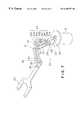
- FIG. 1is a perspective view of a carrying device provided with a frog leg type arm in a first embodiment according to the present invention
- FIG. 2is a diagrammatic view of assistance in explaining a linkage included in the carrying device shown in FIG. 1;
- FIG. 3is a perspective view of a carrying device provided with a frog leg type arm in a second embodiment according to the present invention
- FIG. 4is a diagrammatic view of assistance in explaining the operation of the carrying device shown in FIG. 3;
- FIG. 5is a perspective view of a carrying device provided with a frog leg type arm in a third embodiment according to the present invention.
- FIG. 6is a diagrammatic view of assistance in explaining the operation of the carrying device shown in FIG. 5;
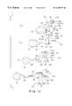
- FIG. 7is a perspective view of a carrying device provided with a parallel linkage type arm in a fourth embodiment according to the present invention.
- FIGS. 8 ( a ) and 8 ( b )are a plan view and a side elevation of the carrying device shown in FIG. 7;
- FIG. 9is a plan view of the carrying device shown in FIG. 7 in a contracted state
- FIG. 10is a diagrammatic view of assistance in explaining a linkage included in the carrying device shown in FIG. 9;
- FIG. 11is a diagrammatic view of assistance in explaining the operation of the carrying device shown in FIG. 9;
- FIG. 12is a diagrammatic view, similar to FIG. 2, of a carrying device provided with a frog leg type arm in a fifth embodiment according to the present invention.
- FIG. 13is a diagrammatic view, similar to FIG. 2, of a carrying device provided with a frog leg type arm in a sixth embodiment according to the present invention.
- FIG. 14is a diagrammatic view, similar to FIG. 2, of a carrying device provided with a frog leg type arm in a seventh embodiment according to the present invention.
- FIG. 15is a diagrammatic view, similar to FIG. 2, of a carrying device provided with a frog leg type arm in an eighth embodiment according to the present invention.
- FIG. 16is a diagrammatic view, similar to FIG. 2, of a carrying device provided with a parallel linkage type arm in a ninth embodiment according to the present invention.
- FIG. 17is a diagrammatic view, similar to FIG. 2, of a carrying device provided with a parallel linkage type arm in a tenth embodiment according to the present invention.
- FIGS. 1 to 17Preferred embodiments of the present invention will be described with reference to FIGS. 1 to 17 .
- a carrying device in a first embodimentincludes a drive shaft 1 formed by coaxially combining first and second drive shafts, not shown, a support member 2 supporting the drive shaft 1 in its central part and housing a driving device for driving the drive shaft 1 , a frog leg type arm 3 having a base end part connected to the drive shaft 1 supported on the support member 2 , a wafer holder 4 connected to a front end part of the frog leg type arm 3 , and a posture maintaining linkage 5 for restricting the turning of the wafer holder 4 to maintain the wafer holder 4 always in a fixed posture.
- the first drive shaft of the drive shaft 1is a hollow shaft and the second drive shaft is extended through the first drive shaft.
- the first and the second drive shaftare connected with a driving device and are driven for turning in the normal direction and the reverse direction (in the opposite directions), respectively.
- the frog leg type arm 3is extended and contracted by turning the first and the second drive shaft through the same angle in the opposite directions, respectively. Turning of the first and the second drive shaft to a same direction by a same amount can change the carrying direction of the frog leg type arm 3 .
- the frog leg type arm 3has a first drive arm 6 A having a base end part connected to the first drive shaft and capable of being turned in opposite directions, a second drive arm 6 B having a base end part connected to the second drive shaft and capable of being turned in opposite directions, a first front arm 8 A having a base end part pivotally connected to a front end part of the first drive arm 6 A by a first joint 7 so as to be able to turn in opposite directions, and a second front arm 8 B having a base end part pivotally connected to a front end part of the second drive arm 6 B by a second joint 9 so as to be able to turn in opposite directions.
- the first front arm 8 A and the second front arm 8 Bhave front end parts pivotally connected to a middle part of a base end part of the wafer holder 4 by third and fourth joints 10 (hereinafter referred to simply as “joints 10 ”).
- the first front arm 8 A and the second front arm 8 Bare able to turn relative to the base end part of the wafer holder 4 in opposite directions.
- the first front arm 8 A and the second front arm 8 Bare slightly longer than the first drive arm 6 A and the second drive arm 6 B.
- the wafer holder 4is interlocked with the pair of the first front arm 8 A and the second front arm 8 B by the posture maintaining linkage 5 .
- the posture maintaining linkage 5includes a first link 5 B having one end pivotally connected to a middle part of the first front arm 8 A by a pivot 5 A, a second link 5 E having one end part pivotally connected to the other end of the first link 5 B by a pivot 5 C and the other end pivotally connected to the base end part of the wafer holder 4 by a pivot 5 D disposed at a position on the front side of the joints 10 in the base end part of the wafer holder 4 , and a third link 5 H having one end pivotally connected to a part of the second link 5 E near the pivot 5 D by a pivot 5 F and the other end pivotally connected to a part of the second front arm 8 B near the front end of the same by a pivot 5 G.
- a part of the wafer holder 4 between the joint 10 and the pivot 5 Dserves as a fourth link 5 I of the posture maintaining linkage 5 .
- FIG. 2is a diagrammatic view of assistance in explaining the frog leg type arm 3 and the posture maintaining linkage 5 shown FIG. 1 .
- the posture maintaining linkage 5will be described with reference to FIG. 2 .
- the first link 5 B and the fourth link 5 Ihave the same length and the length of the second link 5 E is equal to the distance between the joint 10 and the pivot 5 A.
- the pivots 5 A, 5 C and 5 D and the joint 10comprises a first antiparallel linkage.
- the third link 5 H and the fourth link 5 Ihave the same length, the length of a part of the second link 5 E between the pivots 5 D and 5 F is equal to that of a part of the second front arm 8 B between the pivot 5 G and the joint 10 .
- the pivots 5 D, 5 F and 5 G and the joint 10comprises a second antiparallel linkage.
- the ratio of the length of the second link 5 E to that of the first link 5 Bis equal to the ratio of the length of the third link 5 H to that of the part between the pivots 5 D and 5 F. Folding up a parallel linkage along a diagonal forms an antiparallel linkage.
- the angle between the links extending from the pivot 5 Ais equal to that between the links extending from the pivot 5 D
- the angle between the links extending from the pivot 5 Cis equal to that between the links extending from the joint 10
- the angle between the links extending from the pivot 5 Dis equal to that between the links extending from the pivot 5 G
- the angle between the links extending from the pivot 5 Fis equal to that between the links extending from the joint 10 .
- the first and the second antiparallel linkageare similar in shape and the corresponding angles between the corresponding link are always the same regardless of the position of the frog leg type arm 3 .
- the angle between the links extending from the joint 10 of the first antiparallel linkageis always equal to that between the links joined on the joint 10 of the second antiparallel linkage.
- an extension of the fourth link 5 Ii.e., a part of the wafer holder 4 , always bisects the angle between the first front arm 8 A and the second front arm 8 B regardless of the position of the frog leg type arm 3 .
- the posture maintaining linkage 5maintains the wafer holder 4 always in a symmetrical position on the front end part of the frog leg type arm 3 , the wafer holder 4 can be moved straight as the frog leg type arm 3 is extended or contracted without deviation to carry a wafer accurately to a desired position.
- FIG. 3shows a carrying device in a second embodiment according to the present invention.
- a frog leg type arm 3includes a first drive arm 6 A, a second drive arm 6 B, a first front arm 8 A and a second front arm 8 B, which are formed in the same length to give the frog leg type arm 3 a long stroke.
- the frog leg type arm 3 of the carrying device in the first embodimentis at the uncontrollable and unstable point when the frog leg type arm 3 is contracted such that the first drive arm 6 A and the second drive arm 6 B are in the same straight line on the support member 2 and the joint 10 joining the first front arm 8 A and the second front arm 8 B overlies the drive shaft 1 .
- the joint 10 overlying the drive shaft 1is able to move either forward or backward and is unrestrained. Consequently, the frog leg type arm 3 is unable to function.
- the frog leg type arm 3 of the second embodimentis provided with an uncontrollable and unstable point avoidance linkage 11 to avoid the uncontrollable and unstable point.
- FIG. 3parts of the second embodiment like or corresponding to those of the first embodiment are denoted by the same reference characters.
- the carrying device in the second embodimentis the same as that in the first embodiment, except that the first drive arm 6 A, the second drive arm 6 B, the first front arm 8 A and the second front arm 8 B of the frog leg type arm 3 of the second embodiment have the same length and the frog leg type arm 3 of the second embodiment is provided with the uncontrollable and unstable point avoidance linkage 11 .
- the first drive arm 6 A, the second drive arm 6 B, the first front arm 8 A and the second front arm 8 B of the frog leg type arm 3 of the second embodimenthave the same length and the frog leg type arm 3 of the second embodiment is provided with the uncontrollable and unstable point avoidance linkage 11 .
- the uncontrollable and unstable point avoidance linkage 11 of this embodimentis a parallel linkage including, for example, the first drive arm 6 A, a link 11 A extended in parallel to the first drive arm 6 A, a projecting link 11 C pivotally connected to one end part of the link 11 A by a pivot 11 B, laterally projecting from the first front arm 8 A and interconnecting the pivot 11 B and a first joint 7 , and a projecting link 11 E pivotally connected to the other end part of the link 11 A by a pivot 11 D, laterally projecting from the second drive arm 6 B and connecting a drive shaft 1 and the pivot 11 D.
- the length of the link 11 Ais equal to that of the first drive arm 6 A, and the length of the projecting link 11 C (the distance between the first joint 7 and the pivot 11 B) is equal to that of the projecting link 11 E (the distance between the drive shaft 1 and the pivot 11 D).
- first front arm 8 A and the second front arm 8 Bdo not become unrestrained even if a joint 10 joining the first front arm 8 A and the second front arm 8 B overlies the drive shaft 1 , the first drive arm 6 A and the second drive arm 6 B are in the same straight line and the first front arm 8 A and the second front arm 8 B are superposed on the first drive arm 6 A and the second drive arm 6 B because the frog leg type arm 3 is provided with the uncontrollable and unstable point avoidance linkage 11 .
- the frog leg type arm 3can be smoothly extended either forward or backward according to the turning directions of the first drive arm 6 A and the second drive arm 6 B, so that a wafer holder 4 can be surely moved either forward or backward and the frog leg type arm 3 has a long stroke.
- the wafer holder 4 indicated by continuous lines in FIG. 3carries a single wafer.
- the wafer holder 4is able to move in opposite directions with respect to a support member 2 . Therefore, the carrying device in this embodiment may be provided with a wafer holder 4 ′ having a shape formed by extending a wafer holder of the same shape as the wafer holder 4 from the base end of the wafer holder 4 as indicated by broken lines and capable of holding two wafers.
- FIG. 4The operation of a carrying device capable of carrying two wafers at a time will be described with reference to FIG. 4 .
- One of the holding parts of the wafer holder 4 ′receives a semiconductor wafer W with the frog leg type arm 3 extended straight as shown in FIG. 4 ( a ) by the agency of the posture maintaining linkage 5 .
- the first and the second drive shaft of the drive shaft 1operates to contract the frog leg type arm 3 as shown in FIG. 4 ( b ) and the wafer holder 4 ′ moves straight backward from a position where the same has received the wafer W by the agency of the posture maintaining linkage 5 .
- the first and the second drive arm of the frog leg type arm 3extend perpendicularly to the wafer holder 4 ′ over the support member 2 as shown in FIG. 4 ( c ), and the first and the second front arm are superposed on the first and the second drive arm. Since the uncontrollable and unstable point avoidance linkage 11 avoids an uncontrollable and unstable point, the frog leg type arm 3 extends in the opposite direction as shown in FIG. 4 ( d ) by the agency of the uncontrollable and unstable point avoidance linkage 11 when the first drive arm 6 A and the second drive arm 6 B are driven, even if the first and the second front arms are superposed on the first and the second drive arm.
- the wafer holder 4 ′moves straight in a direction opposite to the direction shown in FIG. 4 ( a ) by the agency of the posture maintaining linkage 5 as shown in FIG. 4 ( d ).
- the frog leg type arm 3extends to a predetermined position to transfer the semiconductor wafer w as shown in FIG. 4 ( e ).
- FIG. 5A carrying device in a third embodiment according to the present invention is shown in FIG. 5, in which parts like or corresponding to those of the carrying device in the second embodiment are denoted by the same reference characters.
- the carrying device in the third embodimentis provided with an link 8 C instead of the second front arm.
- the link 8 Chas one end pivotally connected to a middle part of a first front arm (hereinafter referred to as “front arm”) 8 A and the other end pivotally connected to a middle part of a second drive arm 6 B. Since the third embodiment is not provided with any member corresponding to the second front arm, a pivot 5 A included in a posture maintaining linkage 5 is connected to a front end part 6 C of a second drive arm 6 B instead of to the second arm.
- a frog leg type arm 3 employed in the third embodimentis a first parallel linkage including a first drive arm 6 A, a second drive arm 6 B, the front arm 8 A and the link 8 C. Since the first drive arm 6 A, the second drive arm 8 B and the front arm 8 A are the three sides of a rhombus, the distance between the front end part 6 C of the second drive arm 6 B and a joint 10 is invariable and the frog leg type arm 3 can be extended and contracted by driving the first drive arm 6 A and the second drive arm 6 B.
- an uncontrollable and unstable point avoidance linkage 11operates so that the front arm 8 A may not become unrestrained, the frog leg type arm 3 is able to be extended smoothly according to the turning directions of the first drive arm 6 A and the second drive arm 6 B, a wafer holder 4 ′ can be surely moved either forward or backward and the frog leg type arm 3 has a long stroke. Since a pivot 5 A included in a posture maintaining linkage 5 is connected to the front end part 6 C of the second drive arm 6 B, the pivot 5 A, pivots 5 C and 5 D and a joint 10 comprises a first antiparallel linkage.
- the posture maintaining linkage 5maintains the wafer holder 4 ′ always in a fixed posture so that the wafer holder 4 ′ may move along a straight line without laterally swinging as the frog leg type arm 3 is extended and contracted.
- the wafer holder 4 ′can be surely moved either forward or backward as shown in FIGS. 6 ( a ) to 6 ( e ), so that a wafer can be accurately carried to a desired position.
- the frog leg type arm 3is not provided with any member corresponding to the second front arm, a joint 10 attached to the wafer holder 4 ′ may be thin, so that the wafer holder 4 ′ can be passed through a narrower opening to carry a wafer.
- the first embodimentdoes not employ any steel belts and gears and is provided with the posture maintaining linkage 5 . Therefore, the frog leg type arm 3 operates stably even in a hot, corrosive environment and is capable of accurately and surely carrying a semiconductor wafer W in a fixed posture to a desired position.
- All the first drive arm 6 A, the second drive arm 6 B, the first front arm 8 A and the second front arm 8 B of the second embodiment shown in FIG. 3have the same length and the uncontrollable and unstable point of the frog leg type arm 3 is avoided by the uncontrollable and unstable point avoidance linkage 11 . Therefore the frog leg type arm 3 is able to extend and contract continuously forward and backward with respect to the support member 2 . Therefore, the carrying device can be provided with the wafer holder 4 ′ capable of holding two semiconductor wafers W as shown in FIG. 3 and is able to carry semiconductor wafers W efficiently.
- the second embodimentis capable of exercising the same functions and effects as those that can be exercised by the first embodiment.
- the frog leg type arm 3 of the third embodiment shown in FIG. 5is not provided with any member corresponding to the second front arm, and the joint 10 connected to the wafer holder 4 ′ is thin. Therefore the frog leg type arm 3 of the third embodiment is able to carry wafers through a narrower opening.
- the third embodimentis capable of exercising the same functions and effects as those that can be exercised by the second embodiment.
- a carrying device in a fourth embodiment according to the present inventionincludes a drive shaft 26 formed by coaxially combining first and second drive shafts, not shown, (hereinafter referred to simply as “drive shaft”), a support member 21 supporting the drive shaft 26 in its central part and housing a driving device for driving the drive shaft 26 , a parallel linkage type arm 22 having a base end part connected to the drive shaft 26 supported on the support member 21 , a wafer holder 23 connected to a front end part of the parallel linkage type arm 22 , and a posture maintaining linkage 24 for controlling the posture of the parallel linkage type arm 22 to maintain the wafer holder 23 always in a fixed posture.
- drive shaftformed by coaxially combining first and second drive shafts, not shown, (hereinafter referred to simply as “drive shaft”)
- a support member 21supporting the drive shaft 26 in its central part and housing a driving device for driving the drive shaft 26
- a parallel linkage type arm 22having a base end part connected to the drive shaft 26 supported on the support
- the first drive shaft of the drive shaft 26is a hollow shaft and the second drive shaft is extended through the first drive shaft.
- the first and the second drive shaftare interlocked with a driving device and are driven for turning in the normal and the reverse direction.
- the parallel linkage type arm 22is extended and contracted by turning the second drive shaft in the normal and the reverse direction. Turning the first and the second drive shaft in the same direction through the same angle can change the carrying direction of the parallel linkage type arm 22 .
- the parallel linkage type arm 22includes a shoulder link 25 having a base end part connected to the first drive shaft, a drive arm 27 having a base end part connected to the second drive shaft and capable of being turned in opposite directions, a driven arm 29 having a base end part joined to the other end of the shoulder link 25 by a joint 28 and capable of turning in opposite directions, an elbow link 32 having opposite end parts joined to the front end parts of the drive arm 27 and the driven arm 29 by a second joint 30 and a third joint 31 , respectively, and capable of turning in opposite directions, a first front arm 33 having a base end part joined to the elbow link 32 by the second joint 30 and capable of turning in opposite directions, and a second front arm 34 having a base end part joined to the elbow link 32 by the third joint 31 and capable of turning in the opposite directions.
- the wafer holder 23is joined to the front end parts of the first front arm 33 and the second front arm 34 by a fourth joint 35 and a fifth joint 36 so as to be held in a horizontal position on a front end part of the parallel linkage type arm 22 .
- the drive arm 27 , the driven arm 29 , the first front arm 33 and the second front arm 34have the same length.
- the elbow link 32 , the drive arm 27 and the first front arm 33are interlocked by a posture maintaining linkage 24 .
- the posture maintaining linkage 24includes a first link 24 B having one end pivotally connected to a substantially middle part of the drive arm 27 by a pivot 24 A, a second link 24 E having one end pivotally connected to the other end of the first link 24 B by a pivot 24 C and the other end pivotally connected to a part of the elbow link 32 extending beyond the pivot 30 by a pivot 24 D, and a third link 24 H having one end pivotally connected to a part of the first front arm 33 extending beyond the second joint 30 by a pivot 24 F and the other end pivotally connected to a part of the second link 24 E by a pivot 24 G.
- the posture maintaining linkage 24will be described with reference to FIG. 10 showing the parallel linkage type arm 22 and the posture maintaining linkage 24 shown in FIG. 9 .
- the parallel linkage type arm 22has a first parallel linkage including the fixed shoulder link 25 , the drive arm 27 , the driven arm 29 and the elbow link 32 , and a second parallel linkage including the elbow link 32 , the first front arm 33 , the second front arm 34 and a part of the wafer holder 23 between the joints 35 and 36 .
- the length of the first link 24 Bis equal to the distance between the second joint 30 and the pivot 24 D
- the length of the second link 24 Eis equal to the length of a part of the drive arm 27 between the second joint 30 and the pivot 24 A
- the pivots 24 A, 24 C and 24 D and the joint 30comprises a first antiparallel linkage.
- the length of a part of the drive arm 27 between the second joint 30 and the pivot 24 Fis equal to that of a part of the second link 24 E between the pivots 24 D and 24 G.
- the length of the third link 24 His equal to a part of the elbow link 32 between the second joint 30 and the pivot 24 D.
- the pivots 24 D, 24 G and 24 F and the joint 30comprises a second antiparallel linkage.
- the ratio of the distance between the pivot 24 A and the second joint 30 to the length of the first link 24 Bis equal to the ratio of the length of the third link 24 H to the distance between the second joint 30 and the pivot 24 F.
- the angle between the links extending from the pivot 24 Ais equal to that between the links extending from the pivot 24 D
- an angle between the links extending from the pivot 24 Cis equal to that between the links extending from the joint 30
- the angle between the links extending from the pivot 24 Dis equal to that between the links extending from the pivot 24 F
- the angle between the links extending from the pivot 24 Gis equal to that between the links extending from the joint 30 .
- the first and the second antiparallel linkageare similar in shape and the corresponding angles between the corresponding link are always the same regardless of the position of the parallel linkage type arm 22 .
- the angle between the links extending from the joint 30 of the first antiparallel linkageis always equal to that between the links extending from the joint 30 of the second antiparallel linkage. Therefore the elbow link 32 always bisects an angle between the drive arm 27 and the first front arm 33 regardless of the position of the parallel linkage type arm 22 .
- the first front arm 33turns clockwise through the same angle based on the action of the posture maintaining linkage 24 because the elbow link 32 is restrained from turning by the first parallel linkage. Consequently, the wafer holder 23 moves along a straight line over the shoulder link 25 to carry a semiconductor wafer W accurately to a desired position on an extension of the shoulder link 25 .
- the drive arm 27 and the driven arm 29turn counterclockwise, the first front arm 33 and the second front arm 34 are turned clockwise by the action of the posture maintaining linkage, the wafer holder 23 is moved along a straight line past the shoulder link 25 as shown in FIG. 11 ( c ) to a wafer transfer position shown in FIG. 11 ( d ) to transfer a semiconductor wafer W to a wafer receiving member.
- the wafer holder 23is able to operate stably in a hot, corrosive environment, moves always along the straight line extending over the shoulder link 25 always in a fixed posture and is able to carry the semiconductor wafer W accurately to a desired position.
- the present inventionmay be embodied by frog leg type carrying devices shown in FIGS. 12 to 15 .
- the frog leg type carrying devices shown in FIGS. 12 to 15are capable of exercising the same functions and effects as those exercised by the carrying devices in the first and the second embodiment.
- the carrying device shown in FIG. 12includes a frog leg type arm 32 , a wafer holder 33 , and a posture maintaining linkage 34 interconnecting the wafer holder 33 and the frog leg type arm 32 .
- the frog leg type arm 32includes a first drive arm 32 A, a second drive arm 32 B, a first front arm 32 C and a second front arm 32 D.
- the frog leg type arm 32is connected to the wafer holder 33 by a joint 35 .
- the posture maintaining linkage 34includes a first link 34 B having one end part pivotally connected to the first front arm 32 C by a pivot 34 A, a second link 34 E having one end part pivotally connected to the other end part of the first link 34 B by a pivot 34 C and the other end part pivotally connected to a part of the wafer holder 33 on an extended line of a joint 35 on the wafer holder 33 by a pivot 34 D, a third link 34 G having one end part pivotally connected to a middle part of the second link 34 E by a pivot 34 F, a fourth link 34 I having one end part pivotally connected to the other end part of the third link 34 G by a pivot 34 H and extending in parallel to the second link 34 E, and a fifth link 34 K having one end part pivotally connected to the other end part of the fourth link 34 I by a pivot 34 J and the other end part pivotally connected to the wafer holder 33 by a pivot 34 D and extending in parallel to the third link 34 G.
- the fourth link 34 Iis
- the length of the first link 34 Bis equal to the distance between the pivot 34 D and the joint 35
- the length of the second link 34 Eis equal to the distance between the pivot 34 A and the joint 35
- the pivots 34 A, 34 C and 34 D and the joint 35comprises a first antiparallel linkage.
- the distance between the pivot 34 D and the joint 35is equal to the distance between the pivot 34 L and a point 36 on the second link 34 E where a line (chain line) extending from the pivot 34 L in parallel to the fifth link 34 K intersects the second link 34 E, the distance between the pivot 34 D and the point 36 is equal to the distance between the pivot 34 L and the joint 35 , and the pivot 34 D, the point 36 , the pivot 34 L and the joint 35 comprises a second antiparallel linkage.
- the ratio of the length of the second link 34 E to that of the first link 34 Bis equal to the ratio of the distance between the pivot 34 D and the joint 35 to the distance between the pivot 34 D and the point 36 .
- the angle between the second link 34 E and a line segment between the pivot 34 D and the joint 35is common to the first and the second antiparallel linkage.
- the first and the second antiparallel linkageare always similar in shape and the angle between the links extending from the joint 35 of the first antiparallel linkage is equal to that between the links extending from the joint 35 of the second antiparallel linkage regardless of the condition of the frog leg type arm 32 .
- a line connecting the pivot 34 D of the wafer holder 33 and the joint 35always bisects the angle between the first front arm 32 C and the second front arm 32 D, and the wafer holder 33 is maintained always in a fixed posture without being turned laterally.
- the carrying device shown in FIG. 13includes a frog leg type arm 42 , a wafer holder 43 , and a posture maintaining linkage 44 interconnecting the wafer holder 43 and the frog leg type arm 42 .
- the frog leg type arm 42includes a first drive arm 42 A, a second drive arm 42 B, a first front arm 42 C and a second front arm 42 D.
- the frog leg type arm 42is connected to the wafer holder 43 by a joint 45 .
- the posture maintaining linkage 44includes a first link 44 B having one end part pivotally connected to the first front arm 42 C by a pivot 44 A, a second link 44 D having one end part pivotally connected to the other end part of the first link 44 B by a pivot 44 C, a third link 44 F, which is a part of a base part of the wafer holder 43 extending on a center axis on the side of the back end of the wafer holder 43 with respect to the joint 45 or an extension of the wafer holder 43 , having one end part pivotally connected to the other end part of the second link 44 D by a pivot 44 E and the other end part connected to the joint 45 , a fourth link 44 G having one end part pivotally connected to the other end part of the first link 44 B by a pivot 44 C, a fifth link 44 J having one end part pivotally connected to the other end part of the fourth link 44 G by a pivot 44 H and the other end connected to a pivot 44 I on the second front arm 42 D, and a
- the length of the first link 44 Bis equal to that of the third link 44 F
- the length of the second link 44 Dis equal to the distance between the pivot 44 A of the first front arm 42 C and the joint 45
- the pivots 44 A, 44 C and 44 E and the joint 45comprises a first antiparallel linkage.
- the length of the second link 44 Dis equal to that of the fifth link 44 L
- the length of the fourth link 44 Gis equal to the distance between the pivot 44 E in the base end part of the wafer holder 43 and the pivot 44 K
- the pivots 44 C, 44 E, 44 K and 44 Hcomprises a second antiparallel linkage.
- the ratio of the length of the second link 44 D to that of the first link 44 Bis equal to the ratio of the length of the fourth link 44 G to that of the second link 44 D.
- the angle between the second link 44 D and a line segment between the pivot 44 E and the joint 45is common to the first and the second antiparallel linkage.
- the first and the second antiparallel linkageare always similar in shape regardless of the condition of the frog leg type arm 42 .
- Lines connecting the pivots 44 I, 44 H and 44 K and the joint 45form a parallelogram.
- the angle between the links extending from the joint 35 of the first antiparallel linkageis always equal to the angle between the links extending from the pivot 44 K of the second antiparallel linkage
- the angle between the links extending from the pivot 44 K and that between the second front arm 42 D and a line segment between the pivot 44 E and the joint 45is equal to that between the links extending from the joint 45 of the first antiparallel linkage. Therefore a line connecting the pivots 44 E and 44 K always bisects the angle between the first front arm 42 C and the second front arm 42 D, and the wafer holder 43 is maintained always in a fixed posture without being turned laterally.
- the carrying device shown in FIG. 14includes a frog leg type arm 52 , a wafer holder 53 , and a posture maintaining linkage 54 interconnecting the wafer holder 53 and the frog leg type arm 52 .
- the frog leg type arm 52includes a first drive arm 52 A, a second drive arm 52 B, a first front arm 52 C and a second front arm 52 D.
- the frog leg type arm 52is connected to the wafer holder 53 by joints 55 and 56 disposed on a line perpendicular to the length of the base end part of the wafer holder 53 .
- the posture maintaining linkage 54includes a first fixed link 54 B having one end part connected to the first front arm 52 C by a fixed shaft 54 A, a first link 54 D having one end part pivotally connected to the other end part of the first fixed link 54 B by a pivot 54 C, a second link 54 G having one end part pivotally connected to the other end part of the first link 54 D by a pivot 54 E and the other end connected to a pivot 54 F disposed on a base end part of the wafer holder 53 at one of the vertices including joints 55 and 56 of an isosceles triangle, a second fixed link 54 I connected to a fixed shaft 54 H disposed on the second link 54 G, a third link 54 K having one end part pivotally connected to the other end of the second fixed link 54 I by a pivot 54 J, and a third fixed link 54 N having one end part pivotally connected to the other end of the third link 54 K by a pivot 54 L and the other end part connected to a fixed shaft 54 M on the second front arm 52
- the length of the first link 54 Dis equal to the distance between the pivot 54 F and the joint 55 of the wafer holder
- the length of the second link 54 Gis equal to the distance of a line segment between the pivot 54 C and the joint 55 indicated by a broken line
- the pivots 54 C, 54 E and 54 F and the joint 55comprises a first antiparallel linkage.
- the length of the third link 54 Kis equal to the length of a line segment between the pivot 54 F and the joint 56 indicated by a broken line
- the length of a line segment between the pivots 54 F and 54 J indicated by a broken lineis equal to that of a line segment between the pivot 54 L and the joint 56 indicated by a broken line
- the pivots 54 F, 54 J and 54 L and the joint 56comprises a second antiparallel linkage.
- the ratio of the length of the second link 54 G to that of the first link 54 Dis equal to the ratio of the length of the third link 54 K to the distance between the pivots 54 F and 54 J.
- first and the second antiparallel linkagedo not have any angle in common, the first and the second antiparallel linkage are always similar in shape regardless of the condition of the frog leg type arm 52 because the length of the second fixed link 54 I and the distance between the joints 55 and 56 are determined such that the angle between the links extending from the pivot 54 of the first antiparallel linkage is equal to that between the links extending from the pivot 54 F of the second antiparallel linkage.
- the angle between the links extending from the joint 55 of the first antiparallel linkageis always equal to the angle between the links extending from the joint 56 of the second antiparallel linkage and the wafer holder 53 is maintained always in a fixed posture without being turned laterally.
- the carrying device shown in FIG. 15includes a drive shaft 61 of coaxial construction, a frog leg type arm 62 , a wafer holder 63 and a posture maintaining linkage interconnecting the wafer holder 63 and the frog leg type arm 62 .
- the frog leg type arm 62includes a first drive arm 62 A, a second drive arm 62 B, a first front arm 62 C and a second front arm 62 D.
- the frog leg type arm 62is connected to the wafer holder 63 by joints 65 and 66 disposed side by side on a line perpendicular to the length of a base end part of the wafer holder 63 .
- the posture maintaining linkage 64includes a first link 64 A (an extension of the first front arm 62 C) having one end part connected to the joint 65 , a second link 64 C having one end part pivotally connected to the other end part of the first link 64 A by a pivot 64 B, a third link 64 F having a part pivotally connected to the other end part of the second link 64 C by a pivot 64 D and having one end part connected to a pivot 64 E on the wafer holder 63 , and a fourth link 64 I having one end part pivotally connected to the other end part of the third link 64 F by a pivot 64 G and the other end part pivotally connected to the second front arm 62 D by a pivot 64 H.
- the pivot 64 Eis disposed on an extension of a line segment between the joints 65 and 66 . All the links are capable of turning on the pivots.
- the length of the first link 64 Ais equal to the distance between the pivots 64 D and 64 E on the third link 64 F
- the length of the second link 64 Cis equal to the distance between the joint 65 and the pivot 64 E
- the joint 65 and the pivots 64 B, 64 D and 64 Ecomprises a first antiparallel linkage
- the length of the fourth link 64 Iis equal to the distance between the joint 66 and the pivot 64 E
- the length of the third link 64 Fis equal to the distance between the joint 66 and the pivot 64 H on the second front arm 62 D
- the joint 66 and the pivots 64 E, 64 G and 64 Hcomprises a second antiparallel linkage.
- the ratio of the length of the second link 64 C to that of the first link 64 Ais equal to the ratio of the length of the third link 64 F to that of the fourth link 64 I.
- the angle between a line segment between the joint 66 and the pivot 64 E, and the third link 64 Fis common to the first and the second antiparallel linkage. Therefore the first and the second antiparallel linkage are always similar in shape regardless of the condition of the frog leg type arm 62 .
- the angle between the links extending from the joint 65 of the first antiparallel linkageis always equal to that between the links extending from the joint 66 of the second antiparallel linkage and the wafer holder 63 is maintained always in a fixed posture without being turned laterally.
- the present inventionmay be embodied by a parallel linkage type carrying devices shown in FIGS. 16 and 17.
- the same functions and effects as those may be exercised by the fourth embodimentcan be expected of the carrying devices shown in FIGS. 16 and 17.
- the carrying device shown in FIG. 16includes a parallel linkage type arm 73 having a base end part mounted on a drive shaft 71 supported on a support member, not shown, a wafer holder 74 for holding a semiconductor wafer W, connected to a front end part of the parallel linkage type arm 73 , and a posture maintaining linkage 75 for controlling the posture of the parallel linkage type arm 73 to maintain the wafer holder 74 always in a fixed posture.
- the carrying device shown in FIG. 16is the same in construction as the carrying device shown in FIG. 5, except that the former differs from the latter only in the positional relation between the wafer holder 74 and the posture maintaining linkage 75 .
- the wafer holder 74is capable of holding two semiconductor wafers, and the parallel linkage type arm 73 supports the wafer holder 74 in the same manner as that shown in FIG. 5 .
- the parallel linkage type arm 73includes a shoulder link 76 , a drive arm 77 , a driven arm 78 , an elbow link 79 , a first front arm 80 and a second front arm 81 , which are connected by joints 82 to 85 as shown in FIG. 16 .
- the posture maintaining linkage 75 shown in FIG. 16includes a first link 75 B having one end part pivotally connected to an extension of a drive arm 77 by a pivot 75 A, a second link 75 D having a part pivotally connected to the other end part of the first link 75 B by a pivot 75 C, and a third link 75 G having one end part pivotally connected to one end part of the second link 75 D by a pivot 75 E and the other end part pivotally connected to a first front arm 80 by a pivot 75 F.
- the other end of the second link 75 Dis connected to an extension of an elbow link 79 by a pivot 75 H.
- the length of the first link 75 Bis equal to the distance between the joint 83 and the pivot 75 H on the elbow link 79
- the distance between the joint 83 and the pivot 75 A on the drive arm 77is equal to that between the pivots 75 C and 75 H on the second link 75 D
- the pivots 75 A, 75 C and 75 H and the joint 83comprises a first antiparallel linkage.
- the length of the third link 75 Gis equal to the distance between the joint 83 and the pivot 75 H on the elbow link 79
- the length of the second link 75 Dis equal to the distance between the joint 83 and the pivot 75 F on the first front arm 80
- the pivots 75 H, 75 E and 75 F and the joint 83comprises a second antiparallel linkage.
- the ratio of the distance between the joint 83 and the pivot 75 A on the drive arm 77 to the length of the first link 75 Bis equal to the ratio of the length of the third link 75 G to that of the second link 75 D.
- the angle between the links extending from the pivot 75 His common to the first and the second antiparallel linkage.
- Parts of the carrying device shown in FIG. 17 like or corresponding to those of the carrying device shown in FIG. 16are denoted by reference numerals greater by twenty than reference numerals denoting the corresponding parts shown in FIG. 16 and the description thereof will be omitted. Only a posture maintaining linkage 95 included in the carrying device shown in FIG. 17 will be described.
- a parallel linkage type arm 93 shown in FIG. 17a first front arm 100 and a second front arm 101 are not linked directly to a drive arm 97 and a driven arm 98 , and are linked to right-hand parts of an elbow link 99 by joints 106 and 107 .
- the posture maintaining linkage 95includes a first link 95 B having one end part connected to an extension of the drive arm 97 by a pivot 95 A, a second link 95 D having one end part connected to the other end part of the first link 95 B by a pivot 95 C, and a third link 95 E having one end part connected to the other end part of the first link 95 B by the pivot 95 C.
- the other end part of the second link 95 Dis connected to the front arm 101 by a pivot 95 F
- the other end part of the third link 95 Eis connected to the elbow link 99 by a joint 102 .
- the length of the first link 95 Bis equal to the distance between the joint 102 and a joint 103 on the elbow link 99
- the length of the third link 95 Eis equal to the distance between the joint 103 and the pivot 95 A on the drive arm 97
- the pivots 95 A and 95 C and the joints 102 and 103comprises a first antiparallel linkage
- the length of the second link 95 Dis equal to the distance between the joint 102 and a joint 106 on the elbow link 99
- the length of the third link 95 Eis equal to the distance between the joint 106 and the pivot 95 F on the second front arm 101
- the pivots 95 C and 95 F and the joints 102 and 106comprises a second antiparallel linkage.
- the ratio of the length of the third link 95 E to that of the first link 95 Bis equal to the ratio of the length of the second link 95 D to that of the third link 95 E.
- the angle between the links extending from the joint 102is common to the first and the second antiparallel linkage. Therefore all the corresponding angles of the first and the second antiparallel linkage are equal to each other and the first and the second antiparallel linkage are always similar in shape.
- a wafer holder 94When the drive arm 97 is turned counterclockwise by the second drive shaft of a drive shaft 91 , a wafer holder 94 is moved along a straight line over a shoulder link 96 by the agency of the posture maintaining linkage 95 and a wafer holder 94 is able to carry a semiconductor wafer W accurately to a desired position.
- the present inventionis not limited in its practical application to the carrying devices provided with the frog leg type arm or the parallel linkage type arm in the preferred embodiments specifically described herein.
- the present inventionincludes all the carrying devices provided with two antiparallel linkages as a posture maintaining linkage and those provided with a posture maintaining linkage not provided with two practical antiparallel linkages, but provided with two virtual antiparallel linkages formed by fixing the distance between two points to form a virtual link by another parallel linkage or a curved fixed link employed in the carrying devices shown in FIGS. 12 and 14.
Landscapes
- Engineering & Computer Science (AREA)
- Robotics (AREA)
- Physics & Mathematics (AREA)
- Condensed Matter Physics & Semiconductors (AREA)
- General Physics & Mathematics (AREA)
- Manufacturing & Machinery (AREA)
- Computer Hardware Design (AREA)
- Microelectronics & Electronic Packaging (AREA)
- Power Engineering (AREA)
- Mechanical Engineering (AREA)
- Manipulator (AREA)
- Container, Conveyance, Adherence, Positioning, Of Wafer (AREA)
Abstract
Description
The present invention relates to a carrying device employed in, for example, a semiconductor device fabricating system to carry semiconductor wafers, i.e., workpieces.
A conventional carrying device of this kind is used, for example, for carrying semiconductor wafers between a wafer storage chamber and a wafer processing chamber. Known carrying devices of this kind include those provided with a frog leg type arm and those provided with a parallel link type. A carrying device provided with a frog leg type arm has, for example, a pair of drive arms having base end parts connected to a drive shaft, a pair of front arms connected to front end parts of the drive arms by joints, respectively, and a wafer holder connected to front end parts of the front arms. For example, the front end parts of the pair of front arms are connected to the wafer holder by two rotating drums, i.e., upper and lower rotating drums. Two steel belts, i.e., upper and lower steel belts, are crossed around the upper and the lower drum, respectively, to turn the pair of front arms exactly synchronously through the same angle in the opposite directions, respectively. A gear mechanism is used instead of a position maintaining mechanism including rotating drums and steel belts. This position maintaining mechanism maintains the frog leg type arm in a symmetrical shape while the frog leg type arm is bent and stretched. The position maintaining mechanism is used as a power transmitting mechanism for the joint of a parallel link type arm.
In most cases, a hot, corrosive atmosphere is created in, for example, a semiconductor wafer processing chamber. When the arm including belts, such as steel belts, is moved into such a semiconductor wafer processing chamber, the belts are exposed to the hot, corrosive atmosphere. Belts, such as steel belts, have limited heat resistance and corrosion resistance and the hot, corrosive atmosphere in the processing chamber shortens the life of the belts. A carrying device employing gears is not subject to such problems that may be encountered by steel belts. However, gears are apt to produce dust and particles, and backlash between the mating gears causes problem in carrying accuracy.
The present invention has been made to solve the foregoing problems and it is therefore an object of the present invention to provide a carrying device not employing any transmission mechanism including belts and gears, excellent in heat resistance and corrosion resistance, and capable of accurately and surely carrying a workpiece, such as a semiconductor wafer, always in a stable position.
According to a first invention of the present application, a carrying device comprises a support member; first and second shafts supported on the support member; a frog leg type arm having a base end part connected to the first and the second shaft; and a holding member for holding a workpiece, connected to a front end part of the frog leg type arm; wherein the frog leg type arm comprises: a rotatable first drive arm having a base end part mounted on the first shaft, a rotatable second drive arm having a base end part mounted on the second shaft, a first front arm having a base end part pivotally connected to a front end part of the first drive arm by a first joint and a second front arm having a base end part pivotally connected to a front end part of the second drive arm by a second joint; the holding member is connected by third and fourth joints to front end parts of the first and the second front arm; the holding member is linked to the first and the second front arm by a posture maintaining linkage having two similar antiparallel linkages, and the posture maintaining linkage controls turning of the holding member relative to the first and the second front arm.
According to a second invention, in the carrying device according to the first invention, the first and the second shaft are coaxial, the third and the fourth joint are coaxial, the first and the second drive arm and the first and the second front arm have the same length, a parallel linkage is formed by connecting opposite end parts of a links disposed opposite to the first drive arms to the first front arm and the second drive arm, and the parallel linkage has an uncontrollable and unstable point at a position other than a position where the coaxial third and fourth joints overlap the coaxial first and the second shaft.
According to a third invention of the present application, a carrying device comprises: a support member; first and second shafts coaxially supported on the support member; a frog leg type arm having a base end part connected to the first and the second shaft; and a holding member for holding a workpiece, connected to a front end part of the frog leg type arm; wherein the frog leg type arm comprises: a rotatable first drive arm having a base end part mounted on the first shaft, a rotatable second drive arm having a base end part mounted on the second shaft, a front arm having a base end part pivotally connected by a first joint to a front end part of the first drive arm and two links extended in parallel to the first drive arm and having opposite end parts connected to the front arm and the second drive arm; the first and the second drive arm, the front arm and the two links have the same length, and the first and the second drive arm, the front arm and the two links form two parallel linkages; the two parallel linkages have different uncontrollable and unstable points, respectively, and the first and the second drive arm and the front arm form three sides of a rhombus; the holding member is pivotally connected to a front end part of the front arm by a second joint; and the front arm, a front end part of the second drive arm and the holding member are linked by a posture maintaining linkage having two similar antiparallel linkages, and the posture maintaining linkage controls the turning of the holding member relative to the front arm.
According to a fourth invention, in the carrying device in the second or the third invention, the holding member is provided with workpiece holding parts at its opposite ends, and a joint is disposed at a middle point between the holding parts.
According to a fifth invention of the present application, a carrying device comprises: a support member; a parallel linkage type arm having a base end part supported on the support member; and a holding member for holding a workpiece, connected to a front end part of the parallel linkage type arm; wherein the parallel linkage type arm comprises: a first link fixed to the support member, a rotatable drive arm having a base end part mounted on a drive shaft penetrating an end part of the first link, a driven arm having a base end part pivotally connected to the other end of the first link by a first joint, a second link pivotally connected to front end parts of the drive arm and the driven arm by second and third joints, respectively, and first and second front arms having base end parts pivotally connected to the second link; the holding member is connected pivotally to front end parts of the first and the second front arm by fourth and fifth joints; and the drive arm or the driven arm, the second link, and the first or the second front arm are linked by a posture maintaining linkage having two similar antiparallel linkages, and the posture maintaining linkage makes the holding member move along a straight line.
The carrying device according to the first or the fifth invention is provided with a frog leg type arm or a parallel linkage type arm not having a transmission mechanism including belts or gears, excellent in heat resistance and corrosion resistance, and capable of accurately and surely carrying a workpiece, such as a semiconductor wafer, always in a stable position.
According to the second or the fourth invention, the carrying device is provided with a frog leg type arm capable of carrying a workpiece optionally forward or backward relative to the support member in the first invention.
The carrying device according to the third invention is provided with the frog leg type arm capable of exercising the same functions and the same effect as those of the first invention and of carrying a workpiece through a narrow opening.
FIG. 1 is a perspective view of a carrying device provided with a frog leg type arm in a first embodiment according to the present invention;
FIG. 2 is a diagrammatic view of assistance in explaining a linkage included in the carrying device shown in FIG. 1;
FIG. 3 is a perspective view of a carrying device provided with a frog leg type arm in a second embodiment according to the present invention;
FIG. 4 is a diagrammatic view of assistance in explaining the operation of the carrying device shown in FIG. 3;
FIG. 5 is a perspective view of a carrying device provided with a frog leg type arm in a third embodiment according to the present invention;
FIG. 6 is a diagrammatic view of assistance in explaining the operation of the carrying device shown in FIG. 5;
FIG. 7 is a perspective view of a carrying device provided with a parallel linkage type arm in a fourth embodiment according to the present invention;
FIGS.8(a) and8(b) are a plan view and a side elevation of the carrying device shown in FIG. 7;
FIG. 9 is a plan view of the carrying device shown in FIG. 7 in a contracted state;
FIG. 10 is a diagrammatic view of assistance in explaining a linkage included in the carrying device shown in FIG. 9;
FIG. 11 is a diagrammatic view of assistance in explaining the operation of the carrying device shown in FIG. 9;
FIG. 12 is a diagrammatic view, similar to FIG. 2, of a carrying device provided with a frog leg type arm in a fifth embodiment according to the present invention;
FIG. 13 is a diagrammatic view, similar to FIG. 2, of a carrying device provided with a frog leg type arm in a sixth embodiment according to the present invention;
FIG. 14 is a diagrammatic view, similar to FIG. 2, of a carrying device provided with a frog leg type arm in a seventh embodiment according to the present invention;
FIG. 15 is a diagrammatic view, similar to FIG. 2, of a carrying device provided with a frog leg type arm in an eighth embodiment according to the present invention;
FIG. 16 is a diagrammatic view, similar to FIG. 2, of a carrying device provided with a parallel linkage type arm in a ninth embodiment according to the present invention; and
FIG. 17 is a diagrammatic view, similar to FIG. 2, of a carrying device provided with a parallel linkage type arm in a tenth embodiment according to the present invention.
Preferred embodiments of the present invention will be described with reference to FIGS. 1 to17.
Referring to FIGS. 1 and 2, a carrying device in a first embodiment according to the present invention includes adrive shaft 1 formed by coaxially combining first and second drive shafts, not shown, asupport member 2 supporting thedrive shaft 1 in its central part and housing a driving device for driving thedrive shaft 1, a frogleg type arm 3 having a base end part connected to thedrive shaft 1 supported on thesupport member 2, awafer holder 4 connected to a front end part of the frogleg type arm 3, and aposture maintaining linkage 5 for restricting the turning of thewafer holder 4 to maintain thewafer holder 4 always in a fixed posture. The first drive shaft of thedrive shaft 1 is a hollow shaft and the second drive shaft is extended through the first drive shaft. The first and the second drive shaft are connected with a driving device and are driven for turning in the normal direction and the reverse direction (in the opposite directions), respectively. The frogleg type arm 3 is extended and contracted by turning the first and the second drive shaft through the same angle in the opposite directions, respectively. Turning of the first and the second drive shaft to a same direction by a same amount can change the carrying direction of the frogleg type arm 3. When the carrying device in this embodiment is applied to a multichamber processing system, wafers can be carried into and carried out of a plurality of processing chambers.
The frogleg type arm 3 has afirst drive arm 6A having a base end part connected to the first drive shaft and capable of being turned in opposite directions, asecond drive arm 6B having a base end part connected to the second drive shaft and capable of being turned in opposite directions, a firstfront arm 8A having a base end part pivotally connected to a front end part of thefirst drive arm 6A by afirst joint 7 so as to be able to turn in opposite directions, and asecond front arm 8B having a base end part pivotally connected to a front end part of thesecond drive arm 6B by asecond joint 9 so as to be able to turn in opposite directions. The firstfront arm 8A and the secondfront arm 8B have front end parts pivotally connected to a middle part of a base end part of thewafer holder 4 by third and fourth joints10 (hereinafter referred to simply as “joints 10”). Thus the firstfront arm 8A and the secondfront arm 8B are able to turn relative to the base end part of thewafer holder 4 in opposite directions. The firstfront arm 8A and the secondfront arm 8B are slightly longer than thefirst drive arm 6A and thesecond drive arm 6B. Thewafer holder 4 is interlocked with the pair of the firstfront arm 8A and the secondfront arm 8B by theposture maintaining linkage 5.
Referring to FIG. 1, theposture maintaining linkage 5 includes afirst link 5B having one end pivotally connected to a middle part of the firstfront arm 8A by apivot 5A, asecond link 5E having one end part pivotally connected to the other end of thefirst link 5B by apivot 5C and the other end pivotally connected to the base end part of thewafer holder 4 by apivot 5D disposed at a position on the front side of thejoints 10 in the base end part of thewafer holder 4, and athird link 5H having one end pivotally connected to a part of thesecond link 5E near thepivot 5D by apivot 5F and the other end pivotally connected to a part of the secondfront arm 8B near the front end of the same by apivot 5G. As indicated by a broken line in FIG. 2, a part of thewafer holder 4 between thejoint 10 and thepivot 5D serves as a fourth link5I of theposture maintaining linkage 5.
FIG. 2 is a diagrammatic view of assistance in explaining the frogleg type arm 3 and theposture maintaining linkage 5 shown FIG.1. Theposture maintaining linkage 5 will be described with reference to FIG.2. Thefirst link 5B and the fourth link5I have the same length and the length of thesecond link 5E is equal to the distance between thejoint 10 and thepivot 5A. Thepivots joint 10 comprises a first antiparallel linkage. Thethird link 5H and the fourth link5I have the same length, the length of a part of thesecond link 5E between thepivots front arm 8B between thepivot 5G and thejoint 10. Thepivots joint 10 comprises a second antiparallel linkage. The ratio of the length of thesecond link 5E to that of thefirst link 5B is equal to the ratio of the length of thethird link 5H to that of the part between thepivots
In the first antiparallel linkage, the angle between the links extending from thepivot 5A is equal to that between the links extending from thepivot 5D, and the angle between the links extending from thepivot 5C is equal to that between the links extending from the joint10. In the second antiparallel linkage, the angle between the links extending from thepivot 5D is equal to that between the links extending from thepivot 5G, and the angle between the links extending from thepivot 5F is equal to that between the links extending from the joint10. Since the angle between the links extending from thepivot 5D of the first antiparallel linkage is equal to the angle between the links extending from thepivot 5D of the second antiparallel linkage, the first and the second antiparallel linkage are similar in shape and the corresponding angles between the corresponding link are always the same regardless of the position of the frogleg type arm 3. Thus, the angle between the links extending from the joint10 of the first antiparallel linkage is always equal to that between the links joined on the joint10 of the second antiparallel linkage. Therefore an extension of the fourth link5I, i.e., a part of thewafer holder 4, always bisects the angle between the firstfront arm 8A and the secondfront arm 8B regardless of the position of the frogleg type arm 3. Thus theposture maintaining linkage 5 maintains thewafer holder 4 always in a symmetrical position on the front end part of the frogleg type arm 3, thewafer holder 4 can be moved straight as the frogleg type arm 3 is extended or contracted without deviation to carry a wafer accurately to a desired position.
FIG. 3 shows a carrying device in a second embodiment according to the present invention. In the second embodiment, a frogleg type arm 3 includes afirst drive arm 6A, asecond drive arm 6B, a firstfront arm 8A and a secondfront arm 8B, which are formed in the same length to give the frog leg type arm3 a long stroke. The frogleg type arm 3 of the carrying device in the first embodiment is at the uncontrollable and unstable point when the frogleg type arm 3 is contracted such that thefirst drive arm 6A and thesecond drive arm 6B are in the same straight line on thesupport member 2 and the joint10 joining the firstfront arm 8A and the secondfront arm 8B overlies thedrive shaft 1. The joint10 overlying thedrive shaft 1 is able to move either forward or backward and is unrestrained. Consequently, the frogleg type arm 3 is unable to function. The frogleg type arm 3 of the second embodiment is provided with an uncontrollable and unstable point avoidance linkage11 to avoid the uncontrollable and unstable point.
In FIG. 3 parts of the second embodiment like or corresponding to those of the first embodiment are denoted by the same reference characters. The carrying device in the second embodiment is the same as that in the first embodiment, except that thefirst drive arm 6A, thesecond drive arm 6B, the firstfront arm 8A and the secondfront arm 8B of the frogleg type arm 3 of the second embodiment have the same length and the frogleg type arm 3 of the second embodiment is provided with the uncontrollable and unstable point avoidance linkage11. As shown in FIG. 3, the uncontrollable and unstable point avoidance linkage11 of this embodiment is a parallel linkage including, for example, thefirst drive arm 6A, a link11A extended in parallel to thefirst drive arm 6A, a projecting link11C pivotally connected to one end part of the link11A by a pivot11B, laterally projecting from the firstfront arm 8A and interconnecting the pivot11B and a first joint7, and a projecting link11E pivotally connected to the other end part of the link11A by a pivot11D, laterally projecting from thesecond drive arm 6B and connecting adrive shaft 1 and the pivot11D. The length of the link11A is equal to that of thefirst drive arm 6A, and the length of the projecting link11C (the distance between the first joint7 and the pivot11B) is equal to that of the projecting link11E (the distance between thedrive shaft 1 and the pivot11D). Thus the firstfront arm 8A and the secondfront arm 8B do not become unrestrained even if a joint10 joining the firstfront arm 8A and the secondfront arm 8B overlies thedrive shaft 1, thefirst drive arm 6A and thesecond drive arm 6B are in the same straight line and the firstfront arm 8A and the secondfront arm 8B are superposed on thefirst drive arm 6A and thesecond drive arm 6B because the frogleg type arm 3 is provided with the uncontrollable and unstable point avoidance linkage11. Consequently, the frogleg type arm 3 can be smoothly extended either forward or backward according to the turning directions of thefirst drive arm 6A and thesecond drive arm 6B, so that awafer holder 4 can be surely moved either forward or backward and the frogleg type arm 3 has a long stroke.
Thewafer holder 4 indicated by continuous lines in FIG. 3 carries a single wafer. In the carrying device shown in FIG. 3 having the firstfront arm 8A and the secondfront arm 8B and not having any uncontrollable and unstable point, thewafer holder 4 is able to move in opposite directions with respect to asupport member 2. Therefore, the carrying device in this embodiment may be provided with awafer holder 4′ having a shape formed by extending a wafer holder of the same shape as thewafer holder 4 from the base end of thewafer holder 4 as indicated by broken lines and capable of holding two wafers.
The operation of a carrying device capable of carrying two wafers at a time will be described with reference to FIG.4. One of the holding parts of thewafer holder 4′ receives a semiconductor wafer W with the frogleg type arm 3 extended straight as shown in FIG.4(a) by the agency of theposture maintaining linkage 5. The first and the second drive shaft of thedrive shaft 1 operates to contract the frogleg type arm 3 as shown in FIG.4(b) and thewafer holder 4′ moves straight backward from a position where the same has received the wafer W by the agency of theposture maintaining linkage 5.
As thedrive shaft 1 operates further, the first and the second drive arm of the frogleg type arm 3 extend perpendicularly to thewafer holder 4′ over thesupport member 2 as shown in FIG.4(c), and the first and the second front arm are superposed on the first and the second drive arm. Since the uncontrollable and unstable point avoidance linkage11 avoids an uncontrollable and unstable point, the frogleg type arm 3 extends in the opposite direction as shown in FIG.4(d) by the agency of the uncontrollable and unstable point avoidance linkage11 when thefirst drive arm 6A and thesecond drive arm 6B are driven, even if the first and the second front arms are superposed on the first and the second drive arm. Consequently, thewafer holder 4′ moves straight in a direction opposite to the direction shown in FIG.4(a) by the agency of theposture maintaining linkage 5 as shown in FIG.4(d). Finally, the frogleg type arm 3 extends to a predetermined position to transfer the semiconductor wafer w as shown in FIG.4(e).
A carrying device in a third embodiment according to the present invention is shown in FIG. 5, in which parts like or corresponding to those of the carrying device in the second embodiment are denoted by the same reference characters. As shown in FIG. 5, the carrying device in the third embodiment is provided with anlink 8C instead of the second front arm. Thelink 8C has one end pivotally connected to a middle part of a first front arm (hereinafter referred to as “front arm”)8A and the other end pivotally connected to a middle part of asecond drive arm 6B. Since the third embodiment is not provided with any member corresponding to the second front arm, apivot 5A included in aposture maintaining linkage 5 is connected to afront end part 6C of asecond drive arm 6B instead of to the second arm. Thus a frogleg type arm 3 employed in the third embodiment is a first parallel linkage including afirst drive arm 6A, asecond drive arm 6B, thefront arm 8A and thelink 8C. Since thefirst drive arm 6A, thesecond drive arm 8B and thefront arm 8A are the three sides of a rhombus, the distance between thefront end part 6C of thesecond drive arm 6B and a joint10 is invariable and the frogleg type arm 3 can be extended and contracted by driving thefirst drive arm 6A and thesecond drive arm 6B.
Even if the parallel linkage including thelink 8C comes to an uncontrollable and unstable point, an uncontrollable and unstable point avoidance linkage11 operates so that thefront arm 8A may not become unrestrained, the frogleg type arm 3 is able to be extended smoothly according to the turning directions of thefirst drive arm 6A and thesecond drive arm 6B, awafer holder 4′ can be surely moved either forward or backward and the frogleg type arm 3 has a long stroke. Since apivot 5A included in aposture maintaining linkage 5 is connected to thefront end part 6C of thesecond drive arm 6B, thepivot 5A, pivots5C and5D and a joint10 comprises a first antiparallel linkage. Therefore theposture maintaining linkage 5 maintains thewafer holder 4′ always in a fixed posture so that thewafer holder 4′ may move along a straight line without laterally swinging as the frogleg type arm 3 is extended and contracted. Thus, thewafer holder 4′ can be surely moved either forward or backward as shown in FIGS.6(a) to6(e), so that a wafer can be accurately carried to a desired position. Since the frogleg type arm 3 is not provided with any member corresponding to the second front arm, a joint10 attached to thewafer holder 4′ may be thin, so that thewafer holder 4′ can be passed through a narrower opening to carry a wafer.
As mentioned above, the first embodiment does not employ any steel belts and gears and is provided with theposture maintaining linkage 5. Therefore, the frogleg type arm 3 operates stably even in a hot, corrosive environment and is capable of accurately and surely carrying a semiconductor wafer W in a fixed posture to a desired position.
All thefirst drive arm 6A, thesecond drive arm 6B, the firstfront arm 8A and the secondfront arm 8B of the second embodiment shown in FIG. 3 have the same length and the uncontrollable and unstable point of the frogleg type arm 3 is avoided by the uncontrollable and unstable point avoidance linkage11. Therefore the frogleg type arm 3 is able to extend and contract continuously forward and backward with respect to thesupport member 2. Therefore, the carrying device can be provided with thewafer holder 4′ capable of holding two semiconductor wafers W as shown in FIG.3 and is able to carry semiconductor wafers W efficiently. The second embodiment is capable of exercising the same functions and effects as those that can be exercised by the first embodiment.
The frogleg type arm 3 of the third embodiment shown in FIG. 5 is not provided with any member corresponding to the second front arm, and the joint10 connected to thewafer holder 4′ is thin. Therefore the frogleg type arm 3 of the third embodiment is able to carry wafers through a narrower opening. The third embodiment is capable of exercising the same functions and effects as those that can be exercised by the second embodiment.
Referring to FIGS. 7 to9, a carrying device in a fourth embodiment according to the present invention includes adrive shaft 26 formed by coaxially combining first and second drive shafts, not shown, (hereinafter referred to simply as “drive shaft”), asupport member 21 supporting thedrive shaft 26 in its central part and housing a driving device for driving thedrive shaft 26, a parallellinkage type arm 22 having a base end part connected to thedrive shaft 26 supported on thesupport member 21, awafer holder 23 connected to a front end part of the parallellinkage type arm 22, and aposture maintaining linkage 24 for controlling the posture of the parallellinkage type arm 22 to maintain thewafer holder 23 always in a fixed posture. The first drive shaft of thedrive shaft 26 is a hollow shaft and the second drive shaft is extended through the first drive shaft. The first and the second drive shaft are interlocked with a driving device and are driven for turning in the normal and the reverse direction. The parallellinkage type arm 22 is extended and contracted by turning the second drive shaft in the normal and the reverse direction. Turning the first and the second drive shaft in the same direction through the same angle can change the carrying direction of the parallellinkage type arm 22. When the carrying device in this embodiment is applied to a multichamber processing system, wafers can be carried into and carried out of a plurality of processing chambers.
Referring to FIGS. 7 to9, the parallellinkage type arm 22 includes ashoulder link 25 having a base end part connected to the first drive shaft, adrive arm 27 having a base end part connected to the second drive shaft and capable of being turned in opposite directions, a drivenarm 29 having a base end part joined to the other end of theshoulder link 25 by a joint28 and capable of turning in opposite directions, anelbow link 32 having opposite end parts joined to the front end parts of thedrive arm 27 and the drivenarm 29 by a second joint30 and a third joint31, respectively, and capable of turning in opposite directions, a firstfront arm 33 having a base end part joined to theelbow link 32 by the second joint30 and capable of turning in opposite directions, and a secondfront arm 34 having a base end part joined to theelbow link 32 by the third joint31 and capable of turning in the opposite directions.
Thewafer holder 23 is joined to the front end parts of the firstfront arm 33 and the secondfront arm 34 by a fourth joint35 and a fifth joint36 so as to be held in a horizontal position on a front end part of the parallellinkage type arm 22. In the fourth embodiment, thedrive arm 27, the drivenarm 29, the firstfront arm 33 and the secondfront arm 34 have the same length. Theelbow link 32, thedrive arm 27 and the firstfront arm 33 are interlocked by aposture maintaining linkage 24.
Referring to FIGS. 7 to9, theposture maintaining linkage 24 includes afirst link 24B having one end pivotally connected to a substantially middle part of thedrive arm 27 by apivot 24A, asecond link 24E having one end pivotally connected to the other end of thefirst link 24B by apivot 24C and the other end pivotally connected to a part of theelbow link 32 extending beyond thepivot 30 by apivot 24D, and athird link 24H having one end pivotally connected to a part of the firstfront arm 33 extending beyond the second joint30 by apivot 24F and the other end pivotally connected to a part of thesecond link 24E by apivot 24G.
Theposture maintaining linkage 24 will be described with reference to FIG. 10 showing the parallellinkage type arm 22 and theposture maintaining linkage 24 shown in FIG.9. The parallellinkage type arm 22 has a first parallel linkage including the fixedshoulder link 25, thedrive arm 27, the drivenarm 29 and theelbow link 32, and a second parallel linkage including theelbow link 32, the firstfront arm 33, the secondfront arm 34 and a part of thewafer holder 23 between thejoints
In theposture maintaining linkage 24, the length of thefirst link 24B is equal to the distance between the second joint30 and thepivot 24D, the length of thesecond link 24E is equal to the length of a part of thedrive arm 27 between the second joint30 and thepivot 24A, and thepivots drive arm 27 between the second joint30 and thepivot 24F is equal to that of a part of thesecond link 24E between thepivots third link 24H is equal to a part of theelbow link 32 between the second joint30 and thepivot 24D. Thepivots pivot 24A and the second joint30 to the length of thefirst link 24B is equal to the ratio of the length of thethird link 24H to the distance between the second joint30 and thepivot 24F.
In the first antiparallel linkage, the angle between the links extending from thepivot 24A is equal to that between the links extending from thepivot 24D, and an angle between the links extending from thepivot 24C is equal to that between the links extending from the joint30. In the second antiparallel linkage, the angle between the links extending from thepivot 24D is equal to that between the links extending from thepivot 24F and the angle between the links extending from thepivot 24G is equal to that between the links extending from the joint30. Since the angle between the links extending from thepivot 24D of the first antiparallel linkage is equal to that between the links extending from thepivot 24D of the second antiparallel linkage, the first and the second antiparallel linkage are similar in shape and the corresponding angles between the corresponding link are always the same regardless of the position of the parallellinkage type arm 22. Thus, the angle between the links extending from the joint30 of the first antiparallel linkage is always equal to that between the links extending from the joint30 of the second antiparallel linkage. Therefore theelbow link 32 always bisects an angle between thedrive arm 27 and the firstfront arm 33 regardless of the position of the parallellinkage type arm 22.
When thedrive arm 27 is turned counterclockwise through an angle by the second drive shaft of thedrive shaft 26, the firstfront arm 33 turns clockwise through the same angle based on the action of theposture maintaining linkage 24 because theelbow link 32 is restrained from turning by the first parallel linkage. Consequently, thewafer holder 23 moves along a straight line over theshoulder link 25 to carry a semiconductor wafer W accurately to a desired position on an extension of theshoulder link 25.
The operation will be described with reference to FIG.11. As shown in FIG.11(a), when thedrive arm 27 and the drivenarm 29 of the parallellinkage type arm 22 are turned counterclockwise by the second drive shaft of thedrive shaft 26 from a state where the parallellinkage type arm 22 is moved to the right end of the support member, not shown in FIG. 11, by the action of theposture maintaining linkage 24, the firstfront arm 33 and the secondfront arm 34 are turned clockwise relative to thesecond link 32 by the action of theposture maintaining linkage 24. Consequently, thewafer holder 23 is moved to the left along a straight line from a position shown in FIG.11(a), and the firstfront arm 33 and the secondfront arm 34 overlap thedrive arm 27 and the drivenarm 29, and thejoints wafer holder 23 overlie thedrive shaft 26 and the joint28 as shown in FIG.11(b).
As thedrive shaft 1 rotates further, thedrive arm 27 and the drivenarm 29 turn counterclockwise, the firstfront arm 33 and the secondfront arm 34 are turned clockwise by the action of the posture maintaining linkage, thewafer holder 23 is moved along a straight line past theshoulder link 25 as shown in FIG.11(c) to a wafer transfer position shown in FIG.11(d) to transfer a semiconductor wafer W to a wafer receiving member.
As apparent from the foregoing description, since thedrive arm 27 of the parallellinkage type arm 22, theelbow link 32 and the firstfront arm 33 are interlocked by theposture maintaining linkage 24 in the carrying device in the fourth embodiment, thewafer holder 23 is able to operate stably in a hot, corrosive environment, moves always along the straight line extending over theshoulder link 25 always in a fixed posture and is able to carry the semiconductor wafer W accurately to a desired position.
The present invention may be embodied by frog leg type carrying devices shown in FIGS. 12 to15. The frog leg type carrying devices shown in FIGS. 12 to15 are capable of exercising the same functions and effects as those exercised by the carrying devices in the first and the second embodiment.
The carrying device shown in FIG. 12 includes a frogleg type arm 32, awafer holder 33, and aposture maintaining linkage 34 interconnecting thewafer holder 33 and the frogleg type arm 32. The frogleg type arm 32 includes afirst drive arm 32A, asecond drive arm 32B, a firstfront arm 32C and a secondfront arm 32D. The frogleg type arm 32 is connected to thewafer holder 33 by a joint35.
As shown in FIG. 12, theposture maintaining linkage 34 includes afirst link 34B having one end part pivotally connected to the firstfront arm 32C by apivot 34A, asecond link 34E having one end part pivotally connected to the other end part of thefirst link 34B by apivot 34C and the other end part pivotally connected to a part of thewafer holder 33 on an extended line of a joint35 on thewafer holder 33 by apivot 34D, athird link 34G having one end part pivotally connected to a middle part of thesecond link 34E by apivot 34F, a fourth link34I having one end part pivotally connected to the other end part of thethird link 34G by apivot 34H and extending in parallel to thesecond link 34E, and afifth link 34K having one end part pivotally connected to the other end part of the fourth link34I by apivot 34J and the other end part pivotally connected to thewafer holder 33 by apivot 34D and extending in parallel to thethird link 34G. The fourth link34I is connected pivotally to the secondfront arm 32D by a pivot34L.
The length of thefirst link 34B is equal to the distance between thepivot 34D and the joint35, the length of thesecond link 34E is equal to the distance between thepivot 34A and the joint35, and thepivots pivot 34D and the joint35 is equal to the distance between the pivot34L and apoint 36 on thesecond link 34E where a line (chain line) extending from the pivot34L in parallel to thefifth link 34K intersects thesecond link 34E, the distance between thepivot 34D and thepoint 36 is equal to the distance between the pivot34L and the joint35, and thepivot 34D, thepoint 36, the pivot34L and the joint35 comprises a second antiparallel linkage. The ratio of the length of thesecond link 34E to that of thefirst link 34B is equal to the ratio of the distance between thepivot 34D and the joint35 to the distance between thepivot 34D and thepoint 36. The angle between thesecond link 34E and a line segment between thepivot 34D and the joint35 is common to the first and the second antiparallel linkage. Thus, the first and the second antiparallel linkage are always similar in shape and the angle between the links extending from the joint35 of the first antiparallel linkage is equal to that between the links extending from the joint35 of the second antiparallel linkage regardless of the condition of the frogleg type arm 32. Thus a line connecting thepivot 34D of thewafer holder 33 and the joint35 always bisects the angle between the firstfront arm 32C and the secondfront arm 32D, and thewafer holder 33 is maintained always in a fixed posture without being turned laterally.
The carrying device shown in FIG. 13 includes a frogleg type arm 42, a wafer holder43, and aposture maintaining linkage 44 interconnecting the wafer holder43 and the frogleg type arm 42. The frogleg type arm 42 includes afirst drive arm 42A, asecond drive arm 42B, a firstfront arm 42C and a second front arm42D. The frogleg type arm 42 is connected to the wafer holder43 by a joint45.
As shown in FIG. 13, the posture maintaining linkage44 includes a first link44B having one end part pivotally connected to the first front arm42C by a pivot44A, a second link44D having one end part pivotally connected to the other end part of the first link44B by a pivot44C, a third link44F, which is a part of a base part of the wafer holder43 extending on a center axis on the side of the back end of the wafer holder43 with respect to the joint45 or an extension of the wafer holder43, having one end part pivotally connected to the other end part of the second link44D by a pivot44E and the other end part connected to the joint45, a fourth link44G having one end part pivotally connected to the other end part of the first link44B by a pivot44C, a fifth link44J having one end part pivotally connected to the other end part of the fourth link44G by a pivot44H and the other end connected to a pivot44I on the second front arm42D, and a sixth link44L having one end part connected to the pivot44H pivotally connecting the fourth link44G and the fifth link44J and the other end part connected to a pivot44K disposed on a line passing the joint45 of the wafer holder43. The pivots support all the links pivotally.
The length of thefirst link 44B is equal to that of thethird link 44F, the length of thesecond link 44D is equal to the distance between thepivot 44A of the firstfront arm 42C and the joint45, and thepivots second link 44D is equal to that of thefifth link 44L, the length of thefourth link 44G is equal to the distance between thepivot 44E in the base end part of the wafer holder43 and thepivot 44K, and thepivots second link 44D to that of thefirst link 44B is equal to the ratio of the length of thefourth link 44G to that of thesecond link 44D. The angle between thesecond link 44D and a line segment between thepivot 44E and the joint45 is common to the first and the second antiparallel linkage. Thus, the first and the second antiparallel linkage are always similar in shape regardless of the condition of the frogleg type arm 42. Lines connecting thepivots pivot 44K of the second antiparallel linkage, the angle between the links extending from thepivot 44K and that between the second front arm42D and a line segment between thepivot 44E and the joint45, and the angle between the second front arm42D and a line segment between thepivot 44E and the joint45 is equal to that between the links extending from the joint45 of the first antiparallel linkage. Therefore a line connecting thepivots front arm 42C and the second front arm42D, and the wafer holder43 is maintained always in a fixed posture without being turned laterally.
The carrying device shown in FIG. 14 includes a frogleg type arm 52, awafer holder 53, and aposture maintaining linkage 54 interconnecting thewafer holder 53 and the frogleg type arm 52. The frogleg type arm 52 includes afirst drive arm 52A, asecond drive arm 52B, a firstfront arm 52C and a secondfront arm 52D. The frogleg type arm 52 is connected to thewafer holder 53 byjoints wafer holder 53.
As shown in FIG. 14, theposture maintaining linkage 54 includes a firstfixed link 54B having one end part connected to the firstfront arm 52C by a fixedshaft 54A, afirst link 54D having one end part pivotally connected to the other end part of the first fixedlink 54B by apivot 54C, asecond link 54G having one end part pivotally connected to the other end part of thefirst link 54D by apivot 54E and the other end connected to apivot 54F disposed on a base end part of thewafer holder 53 at one of thevertices including joints shaft 54H disposed on thesecond link 54G, a third link54K having one end part pivotally connected to the other end of the second fixed link54I by apivot 54J, and a thirdfixed link 54N having one end part pivotally connected to the other end of the third link54K by apivot 54L and the other end part connected to a fixedshaft 54M on the secondfront arm 52D.
The length of thefirst link 54D is equal to the distance between thepivot 54F and the joint55 of the wafer holder, the length of thesecond link 54G is equal to the distance of a line segment between thepivot 54C and the joint55 indicated by a broken line, and thepivots pivot 54F and the joint56 indicated by a broken line, the length of a line segment between thepivots pivot 54L and the joint56 indicated by a broken line, and thepivots second link 54G to that of thefirst link 54D is equal to the ratio of the length of the third link54K to the distance between thepivots leg type arm 52 because the length of the second fixed link54I and the distance between thejoints pivot 54 of the first antiparallel linkage is equal to that between the links extending from thepivot 54F of the second antiparallel linkage. Thus, the angle between the links extending from the joint55 of the first antiparallel linkage is always equal to the angle between the links extending from the joint56 of the second antiparallel linkage and thewafer holder 53 is maintained always in a fixed posture without being turned laterally.
The carrying device shown in FIG. 15 includes adrive shaft 61 of coaxial construction, a frogleg type arm 62, awafer holder 63 and a posture maintaining linkage interconnecting thewafer holder 63 and the frogleg type arm 62. The frogleg type arm 62 includes afirst drive arm 62A, asecond drive arm 62B, a firstfront arm 62C and a secondfront arm 62D. The frogleg type arm 62 is connected to thewafer holder 63 byjoints wafer holder 63.
As shown in FIG. 15, theposture maintaining linkage 64 includes afirst link 64A (an extension of the firstfront arm 62C) having one end part connected to the joint65, asecond link 64C having one end part pivotally connected to the other end part of thefirst link 64A by apivot 64B, athird link 64F having a part pivotally connected to the other end part of thesecond link 64C by apivot 64D and having one end part connected to apivot 64E on thewafer holder 63, and a fourth link64I having one end part pivotally connected to the other end part of thethird link 64F by apivot 64G and the other end part pivotally connected to the secondfront arm 62D by apivot 64H. Thepivot 64E is disposed on an extension of a line segment between thejoints
The length of thefirst link 64A is equal to the distance between thepivots third link 64F, the length of thesecond link 64C is equal to the distance between the joint65 and thepivot 64E, and the joint65 and thepivots pivot 64E, the length of thethird link 64F is equal to the distance between the joint66 and thepivot 64H on the secondfront arm 62D, and the joint66 and thepivots second link 64C to that of thefirst link 64A is equal to the ratio of the length of thethird link 64F to that of the fourth link64I. The angle between a line segment between the joint66 and thepivot 64E, and thethird link 64F is common to the first and the second antiparallel linkage. Therefore the first and the second antiparallel linkage are always similar in shape regardless of the condition of the frogleg type arm 62. Thus the angle between the links extending from the joint65 of the first antiparallel linkage is always equal to that between the links extending from the joint66 of the second antiparallel linkage and thewafer holder 63 is maintained always in a fixed posture without being turned laterally.
The present invention may be embodied by a parallel linkage type carrying devices shown in FIGS. 16 and 17. The same functions and effects as those may be exercised by the fourth embodiment can be expected of the carrying devices shown in FIGS. 16 and 17.
The carrying device shown in FIG. 16 includes a parallellinkage type arm 73 having a base end part mounted on adrive shaft 71 supported on a support member, not shown, awafer holder 74 for holding a semiconductor wafer W, connected to a front end part of the parallellinkage type arm 73, and aposture maintaining linkage 75 for controlling the posture of the parallellinkage type arm 73 to maintain thewafer holder 74 always in a fixed posture. The carrying device shown in FIG. 16 is the same in construction as the carrying device shown in FIG. 5, except that the former differs from the latter only in the positional relation between thewafer holder 74 and theposture maintaining linkage 75. Thewafer holder 74 is capable of holding two semiconductor wafers, and the parallellinkage type arm 73 supports thewafer holder 74 in the same manner as that shown in FIG.5.
As shown in FIG. 16, the parallellinkage type arm 73 includes ashoulder link 76, adrive arm 77, a drivenarm 78, anelbow link 79, a firstfront arm 80 and a secondfront arm 81, which are connected byjoints 82 to85 as shown in FIG.16.
Theposture maintaining linkage 75 shown in FIG. 16 includes afirst link 75B having one end part pivotally connected to an extension of adrive arm 77 by apivot 75A, asecond link 75D having a part pivotally connected to the other end part of thefirst link 75B by apivot 75C, and athird link 75G having one end part pivotally connected to one end part of thesecond link 75D by apivot 75E and the other end part pivotally connected to a firstfront arm 80 by apivot 75F. The other end of thesecond link 75D is connected to an extension of anelbow link 79 by apivot 75H.
In theposture maintaining linkage 75, the length of thefirst link 75B is equal to the distance between the joint83 and thepivot 75H on theelbow link 79, the distance between the joint83 and thepivot 75A on thedrive arm 77 is equal to that between thepivots second link 75D, and thepivots third link 75G is equal to the distance between the joint83 and thepivot 75H on theelbow link 79, the length of thesecond link 75D is equal to the distance between the joint83 and thepivot 75F on the firstfront arm 80, and thepivots pivot 75A on thedrive arm 77 to the length of thefirst link 75B is equal to the ratio of the length of thethird link 75G to that of thesecond link 75D. The angle between the links extending from thepivot 75H is common to the first and the second antiparallel linkage. Therefore all the corresponding angles of the first and the second antiparallel linkage are equal to each other and the first and the second antiparallel linkage are always similar in shape. When thedrive arm 77 is turned counterclockwise by the second drive shaft of thedrive shaft 71, thewafer holder 74 is moved along a straight line over theshoulder link 76 by the agency of theposture maintaining linkage 75 and thewafer holder 74 is able to carry a semiconductor wafer W accurately to a desired position.
Parts of the carrying device shown in FIG. 17 like or corresponding to those of the carrying device shown in FIG. 16 are denoted by reference numerals greater by twenty than reference numerals denoting the corresponding parts shown in FIG.16 and the description thereof will be omitted. Only aposture maintaining linkage 95 included in the carrying device shown in FIG. 17 will be described. In a parallellinkage type arm 93 shown in FIG. 17, a firstfront arm 100 and a secondfront arm 101 are not linked directly to adrive arm 97 and a drivenarm 98, and are linked to right-hand parts of anelbow link 99 byjoints
As shown in FIG. 17, theposture maintaining linkage 95 includes afirst link 95B having one end part connected to an extension of thedrive arm 97 by a pivot95A, asecond link 95D having one end part connected to the other end part of thefirst link 95B by apivot 95C, and athird link 95E having one end part connected to the other end part of thefirst link 95B by thepivot 95C. The other end part of thesecond link 95D is connected to thefront arm 101 by apivot 95F, and the other end part of thethird link 95E is connected to theelbow link 99 by a joint102.
The length of thefirst link 95B is equal to the distance between the joint102 and a joint103 on theelbow link 99, the length of thethird link 95E is equal to the distance between the joint103 and the pivot95A on thedrive arm 97, and thepivots 95A and95C and thejoints second link 95D is equal to the distance between the joint102 and a joint106 on theelbow link 99, the length of thethird link 95E is equal to the distance between the joint106 and thepivot 95F on the secondfront arm 101, and thepivots joints third link 95E to that of thefirst link 95B is equal to the ratio of the length of thesecond link 95D to that of thethird link 95E. The angle between the links extending from the joint102 is common to the first and the second antiparallel linkage. Therefore all the corresponding angles of the first and the second antiparallel linkage are equal to each other and the first and the second antiparallel linkage are always similar in shape. When thedrive arm 97 is turned counterclockwise by the second drive shaft of adrive shaft 91, awafer holder 94 is moved along a straight line over ashoulder link 96 by the agency of theposture maintaining linkage 95 and awafer holder 94 is able to carry a semiconductor wafer W accurately to a desired position.
The present invention is not limited in its practical application to the carrying devices provided with the frog leg type arm or the parallel linkage type arm in the preferred embodiments specifically described herein. The present invention includes all the carrying devices provided with two antiparallel linkages as a posture maintaining linkage and those provided with a posture maintaining linkage not provided with two practical antiparallel linkages, but provided with two virtual antiparallel linkages formed by fixing the distance between two points to form a virtual link by another parallel linkage or a curved fixed link employed in the carrying devices shown in FIGS. 12 and 14.
Claims (6)
1. A carrying device comprising:
a support member;
first and second shafts supported on the support member;
a frog leg type arm having a base end part connected to the first and the second shaft; and
a holding member for holding a workpiece, connected to a front end part of the frog leg type arm;
wherein the frog leg type arm comprises:
a rotatable first drive arm having a base end part mounted on the first shaft,
a rotatable second drive arm having a base end part mounted on the second shaft,
a first front arm having a base end part pivotally connected to a front end part of the first drive arm by a first joint and
a second front arm having a base end part pivotally connected to a front end part of the second drive arm by a second joint;
the holding member is connected by third and fourth joints to front end parts of the first and the second front arm;
the holding member is linked to the first and the second front arm by a posture maintaining linkage having two similar antiparallel linkages, and the posture maintaining linkage controls turning of the holding member relative to the first and the second front arm.
2. A carrying device according toclaim 1 , wherein the first and the second shaft are coaxial, the third and the fourth joint are coaxial,
the first and the second drive arm and the first and the second front arm have the same length,
a parallel linkage is formed by connecting opposite end parts of a links disposed opposite to the first drive arms to the first front arm and the second drive arm, and
the parallel linkage has an uncontrollable and unstable point at a position other than a position where the coaxial third and fourth joints overlap the coaxial first and the second shaft.
3. A carrying device according toclaim 2 , wherein the holding member is provided with workpiece holding parts at its opposite ends, and a joint is disposed at a middle point between the workpiece holding parts.
4. A carrying device comprising:
a support member;
first and second shafts coaxially supported on the support member;
a frog leg type arm having a base end part connected to the first and the second shaft; and
a holding member for holding a workpiece, connected to a front end part of the frog leg type arm;
wherein the frog leg type arm comprises:
a rotatable first drive arm having a base end part mounted on the first shaft,
a rotatable second drive arm having a base end part mounted on the second shaft,
a front arm having a base end part pivotally connected by a first joint to a front end part of the first drive arm and
two links extended in parallel to the first drive arm and having opposite end parts connected to the front arm and the second drive arm;
the first and the second drive arm, the front arm and the two links have the same length, and the first and the second drive arm, the front arm and the two links form two parallel linkages;
the two parallel linkages have different uncontrollable and unstable points, respectively, and the first and the second drive arm and the front arm form three sides of a rhombus;
the holding member is pivotally connected to a front end part of the front arm by a second joint; and
the front arm, a front end part of the second drive arm and the holding member are linked by a posture maintaining linkage having two similar antiparallel linkages, and the posture maintaining linkage controls the turning of the holding member relative to the front arm.
5. A carrying device according toclaim 4 , wherein the holding member is provided with workpiece holding parts at its opposite ends, and a joint is disposed at a middle point between the workpiece holding parts.
6. A carrying device comprising:
a support member;
a parallel linkage type arm having a base end part supported on the support member; and
a holding member for holding a workpiece, connected to a front end part of the parallel linkage type arm;
wherein the parallel linkage type arm comprises:
a first link fixed to the support member,
a rotatable drive arm having a base end part mounted on a drive shaft penetrating an end part of the first link,
a driven arm having a base end part pivotally connected to the other end of the first link by a first joint,
a second link pivotally connected to front end parts of the drive arm and the driven arm by second and third joints, respectively, and
first and second front arms having base end parts pivotally connected to the second link;
the holding member is connected pivotally to front end parts of the first and the second front arm by fourth and fifth joints; and
the drive arm or the driven arm, the second link, and the first or the second front arm are linked by a posture maintaining linkage having two similar antiparallel linkages, and the posture maintaining linkage makes the holding member move along a straight line.
Priority Applications (1)
| Application Number | Priority Date | Filing Date | Title |
|---|---|---|---|
| US10/218,997US6699003B2 (en) | 1998-11-17 | 2002-08-15 | Carrying device |
Applications Claiming Priority (3)
| Application Number | Priority Date | Filing Date | Title |
|---|---|---|---|
| JP10-343585 | 1998-11-17 | ||
| JP10343585AJP2000150617A (en) | 1998-11-17 | 1998-11-17 | Transporter |
| PCT/JP1999/006358WO2000029176A1 (en) | 1998-11-17 | 1999-11-15 | Conveyor system |
Related Parent Applications (1)
| Application Number | Title | Priority Date | Filing Date |
|---|---|---|---|
| PCT/JP1999/006358A-371-Of-InternationalWO2000029176A1 (en) | 1998-11-17 | 1999-11-15 | Conveyor system |
Related Child Applications (1)
| Application Number | Title | Priority Date | Filing Date |
|---|---|---|---|
| US10/218,997ContinuationUS6699003B2 (en) | 1998-11-17 | 2002-08-15 | Carrying device |
Publications (1)
| Publication Number | Publication Date |
|---|---|
| US6450757B1true US6450757B1 (en) | 2002-09-17 |
Family
ID=18362674
Family Applications (2)
| Application Number | Title | Priority Date | Filing Date |
|---|---|---|---|
| US09/856,097Expired - Fee RelatedUS6450757B1 (en) | 1998-11-17 | 1999-11-15 | Conveyor system |
| US10/218,997Expired - Fee RelatedUS6699003B2 (en) | 1998-11-17 | 2002-08-15 | Carrying device |
Family Applications After (1)
| Application Number | Title | Priority Date | Filing Date |
|---|---|---|---|
| US10/218,997Expired - Fee RelatedUS6699003B2 (en) | 1998-11-17 | 2002-08-15 | Carrying device |
Country Status (7)
| Country | Link |
|---|---|
| US (2) | US6450757B1 (en) |
| EP (1) | EP1207025B1 (en) |
| JP (1) | JP2000150617A (en) |
| KR (1) | KR100617504B1 (en) |
| DE (1) | DE69940220D1 (en) |
| TW (1) | TW444243B (en) |
| WO (1) | WO2000029176A1 (en) |
Cited By (402)
| Publication number | Priority date | Publication date | Assignee | Title |
|---|---|---|---|---|
| US20020150456A1 (en)* | 2001-04-16 | 2002-10-17 | Samsung Electronics Co., Ltd. | Method and apparatus for transferring a wafer |
| US6663333B2 (en)* | 2001-07-13 | 2003-12-16 | Axcelis Technologies, Inc. | Wafer transport apparatus |
| US6675069B2 (en)* | 2001-04-26 | 2004-01-06 | Daihen Corporation | Arm operation mechanism and industrial robot incorporating the same |
| US6840732B2 (en)* | 2000-10-24 | 2005-01-11 | Ulvac, Inc. | Transport apparatus and vacuum processing system using the same |
| US20050079043A1 (en)* | 2003-07-11 | 2005-04-14 | Daihen Corporation | Two-arm transfer robot |
| US7001139B2 (en) | 2001-12-03 | 2006-02-21 | Teijin Seiki Co., Ltd. | Robot arm mechanism |
| US20060214354A1 (en)* | 2003-05-20 | 2006-09-28 | Ishikawajima-Harima Heavy Industries Co., Ltd. | Panel transportation device |
| US20080149461A1 (en)* | 2004-05-10 | 2008-06-26 | Ishikawajima-Harima Heavy Industries Co., Ltd. | Panel Transportation Device |
| US20140321957A1 (en)* | 2011-12-15 | 2014-10-30 | Tazmo Co., Ltd. | Wafer transport robot |
| US8915693B2 (en) | 2010-06-10 | 2014-12-23 | Nabtesco Corporation | Robot arm having lower arm link separable into two parts |
| US20150217456A1 (en)* | 2014-02-04 | 2015-08-06 | Asm Ip Holding B.V. | Anti-slip end-effector for transporting workpiece |
| US20150360373A1 (en)* | 2014-06-11 | 2015-12-17 | Samsung Electronics Co., Ltd. | Link structure |
| US9287149B2 (en) | 2011-01-26 | 2016-03-15 | Nabtesco Corporation | Wafer Handling Robot |
| US9324811B2 (en) | 2012-09-26 | 2016-04-26 | Asm Ip Holding B.V. | Structures and devices including a tensile-stressed silicon arsenic layer and methods of forming same |
| US9384987B2 (en) | 2012-04-04 | 2016-07-05 | Asm Ip Holding B.V. | Metal oxide protective layer for a semiconductor device |
| US9394608B2 (en) | 2009-04-06 | 2016-07-19 | Asm America, Inc. | Semiconductor processing reactor and components thereof |
| US9404587B2 (en) | 2014-04-24 | 2016-08-02 | ASM IP Holding B.V | Lockout tagout for semiconductor vacuum valve |
| US9412564B2 (en) | 2013-07-22 | 2016-08-09 | Asm Ip Holding B.V. | Semiconductor reaction chamber with plasma capabilities |
| US9447498B2 (en) | 2014-03-18 | 2016-09-20 | Asm Ip Holding B.V. | Method for performing uniform processing in gas system-sharing multiple reaction chambers |
| US9455138B1 (en) | 2015-11-10 | 2016-09-27 | Asm Ip Holding B.V. | Method for forming dielectric film in trenches by PEALD using H-containing gas |
| US9478415B2 (en) | 2015-02-13 | 2016-10-25 | Asm Ip Holding B.V. | Method for forming film having low resistance and shallow junction depth |
| US9484191B2 (en) | 2013-03-08 | 2016-11-01 | Asm Ip Holding B.V. | Pulsed remote plasma method and system |
| US9543180B2 (en) | 2014-08-01 | 2017-01-10 | Asm Ip Holding B.V. | Apparatus and method for transporting wafers between wafer carrier and process tool under vacuum |
| US9558931B2 (en) | 2012-07-27 | 2017-01-31 | Asm Ip Holding B.V. | System and method for gas-phase sulfur passivation of a semiconductor surface |
| US9556516B2 (en) | 2013-10-09 | 2017-01-31 | ASM IP Holding B.V | Method for forming Ti-containing film by PEALD using TDMAT or TDEAT |
| US9589770B2 (en) | 2013-03-08 | 2017-03-07 | Asm Ip Holding B.V. | Method and systems for in-situ formation of intermediate reactive species |
| US9607837B1 (en) | 2015-12-21 | 2017-03-28 | Asm Ip Holding B.V. | Method for forming silicon oxide cap layer for solid state diffusion process |
| US9605342B2 (en) | 2012-09-12 | 2017-03-28 | Asm Ip Holding B.V. | Process gas management for an inductively-coupled plasma deposition reactor |
| US9627221B1 (en) | 2015-12-28 | 2017-04-18 | Asm Ip Holding B.V. | Continuous process incorporating atomic layer etching |
| US9640416B2 (en) | 2012-12-26 | 2017-05-02 | Asm Ip Holding B.V. | Single-and dual-chamber module-attachable wafer-handling chamber |
| US9647114B2 (en) | 2015-08-14 | 2017-05-09 | Asm Ip Holding B.V. | Methods of forming highly p-type doped germanium tin films and structures and devices including the films |
| US9659799B2 (en) | 2012-08-28 | 2017-05-23 | Asm Ip Holding B.V. | Systems and methods for dynamic semiconductor process scheduling |
| US9657845B2 (en) | 2014-10-07 | 2017-05-23 | Asm Ip Holding B.V. | Variable conductance gas distribution apparatus and method |
| US9711345B2 (en) | 2015-08-25 | 2017-07-18 | Asm Ip Holding B.V. | Method for forming aluminum nitride-based film by PEALD |
| US9735024B2 (en) | 2015-12-28 | 2017-08-15 | Asm Ip Holding B.V. | Method of atomic layer etching using functional group-containing fluorocarbon |
| US9754779B1 (en) | 2016-02-19 | 2017-09-05 | Asm Ip Holding B.V. | Method for forming silicon nitride film selectively on sidewalls or flat surfaces of trenches |
| US9793115B2 (en) | 2013-08-14 | 2017-10-17 | Asm Ip Holding B.V. | Structures and devices including germanium-tin films and methods of forming same |
| US9790595B2 (en) | 2013-07-12 | 2017-10-17 | Asm Ip Holding B.V. | Method and system to reduce outgassing in a reaction chamber |
| US9793135B1 (en) | 2016-07-14 | 2017-10-17 | ASM IP Holding B.V | Method of cyclic dry etching using etchant film |
| US9793148B2 (en) | 2011-06-22 | 2017-10-17 | Asm Japan K.K. | Method for positioning wafers in multiple wafer transport |
| US9812320B1 (en) | 2016-07-28 | 2017-11-07 | Asm Ip Holding B.V. | Method and apparatus for filling a gap |
| US9859151B1 (en) | 2016-07-08 | 2018-01-02 | Asm Ip Holding B.V. | Selective film deposition method to form air gaps |
| US9887082B1 (en) | 2016-07-28 | 2018-02-06 | Asm Ip Holding B.V. | Method and apparatus for filling a gap |
| US9891521B2 (en) | 2014-11-19 | 2018-02-13 | Asm Ip Holding B.V. | Method for depositing thin film |
| US9890456B2 (en) | 2014-08-21 | 2018-02-13 | Asm Ip Holding B.V. | Method and system for in situ formation of gas-phase compounds |
| US9892908B2 (en) | 2011-10-28 | 2018-02-13 | Asm America, Inc. | Process feed management for semiconductor substrate processing |
| US9899405B2 (en) | 2014-12-22 | 2018-02-20 | Asm Ip Holding B.V. | Semiconductor device and manufacturing method thereof |
| US9899291B2 (en) | 2015-07-13 | 2018-02-20 | Asm Ip Holding B.V. | Method for protecting layer by forming hydrocarbon-based extremely thin film |
| US9905420B2 (en) | 2015-12-01 | 2018-02-27 | Asm Ip Holding B.V. | Methods of forming silicon germanium tin films and structures and devices including the films |
| US9909214B2 (en) | 2015-10-15 | 2018-03-06 | Asm Ip Holding B.V. | Method for depositing dielectric film in trenches by PEALD |
| US9916980B1 (en) | 2016-12-15 | 2018-03-13 | Asm Ip Holding B.V. | Method of forming a structure on a substrate |
| US9960072B2 (en) | 2015-09-29 | 2018-05-01 | Asm Ip Holding B.V. | Variable adjustment for precise matching of multiple chamber cavity housings |
| US10032628B2 (en) | 2016-05-02 | 2018-07-24 | Asm Ip Holding B.V. | Source/drain performance through conformal solid state doping |
| US10043661B2 (en) | 2015-07-13 | 2018-08-07 | Asm Ip Holding B.V. | Method for protecting layer by forming hydrocarbon-based extremely thin film |
| US10083836B2 (en) | 2015-07-24 | 2018-09-25 | Asm Ip Holding B.V. | Formation of boron-doped titanium metal films with high work function |
| US10087525B2 (en) | 2015-08-04 | 2018-10-02 | Asm Ip Holding B.V. | Variable gap hard stop design |
| US10090316B2 (en) | 2016-09-01 | 2018-10-02 | Asm Ip Holding B.V. | 3D stacked multilayer semiconductor memory using doped select transistor channel |
| US10087522B2 (en) | 2016-04-21 | 2018-10-02 | Asm Ip Holding B.V. | Deposition of metal borides |
| US10103040B1 (en) | 2017-03-31 | 2018-10-16 | Asm Ip Holding B.V. | Apparatus and method for manufacturing a semiconductor device |
| USD830981S1 (en) | 2017-04-07 | 2018-10-16 | Asm Ip Holding B.V. | Susceptor for semiconductor substrate processing apparatus |
| US10134757B2 (en) | 2016-11-07 | 2018-11-20 | Asm Ip Holding B.V. | Method of processing a substrate and a device manufactured by using the method |
| US10167557B2 (en) | 2014-03-18 | 2019-01-01 | Asm Ip Holding B.V. | Gas distribution system, reactor including the system, and methods of using the same |
| US10177025B2 (en) | 2016-07-28 | 2019-01-08 | Asm Ip Holding B.V. | Method and apparatus for filling a gap |
| US10179947B2 (en) | 2013-11-26 | 2019-01-15 | Asm Ip Holding B.V. | Method for forming conformal nitrided, oxidized, or carbonized dielectric film by atomic layer deposition |
| US10190213B2 (en) | 2016-04-21 | 2019-01-29 | Asm Ip Holding B.V. | Deposition of metal borides |
| US10211308B2 (en) | 2015-10-21 | 2019-02-19 | Asm Ip Holding B.V. | NbMC layers |
| US10229833B2 (en) | 2016-11-01 | 2019-03-12 | Asm Ip Holding B.V. | Methods for forming a transition metal nitride film on a substrate by atomic layer deposition and related semiconductor device structures |
| US10236177B1 (en) | 2017-08-22 | 2019-03-19 | ASM IP Holding B.V.. | Methods for depositing a doped germanium tin semiconductor and related semiconductor device structures |
| US10249524B2 (en) | 2017-08-09 | 2019-04-02 | Asm Ip Holding B.V. | Cassette holder assembly for a substrate cassette and holding member for use in such assembly |
| US10249577B2 (en) | 2016-05-17 | 2019-04-02 | Asm Ip Holding B.V. | Method of forming metal interconnection and method of fabricating semiconductor apparatus using the method |
| US10262859B2 (en) | 2016-03-24 | 2019-04-16 | Asm Ip Holding B.V. | Process for forming a film on a substrate using multi-port injection assemblies |
| US10269558B2 (en) | 2016-12-22 | 2019-04-23 | Asm Ip Holding B.V. | Method of forming a structure on a substrate |
| US10276355B2 (en) | 2015-03-12 | 2019-04-30 | Asm Ip Holding B.V. | Multi-zone reactor, system including the reactor, and method of using the same |
| US10283353B2 (en) | 2017-03-29 | 2019-05-07 | Asm Ip Holding B.V. | Method of reforming insulating film deposited on substrate with recess pattern |
| US10290508B1 (en) | 2017-12-05 | 2019-05-14 | Asm Ip Holding B.V. | Method for forming vertical spacers for spacer-defined patterning |
| US10312055B2 (en) | 2017-07-26 | 2019-06-04 | Asm Ip Holding B.V. | Method of depositing film by PEALD using negative bias |
| US10319588B2 (en) | 2017-10-10 | 2019-06-11 | Asm Ip Holding B.V. | Method for depositing a metal chalcogenide on a substrate by cyclical deposition |
| US10322384B2 (en) | 2015-11-09 | 2019-06-18 | Asm Ip Holding B.V. | Counter flow mixer for process chamber |
| US10340135B2 (en) | 2016-11-28 | 2019-07-02 | Asm Ip Holding B.V. | Method of topologically restricted plasma-enhanced cyclic deposition of silicon or metal nitride |
| US10343920B2 (en) | 2016-03-18 | 2019-07-09 | Asm Ip Holding B.V. | Aligned carbon nanotubes |
| US10361201B2 (en) | 2013-09-27 | 2019-07-23 | Asm Ip Holding B.V. | Semiconductor structure and device formed using selective epitaxial process |
| US10364496B2 (en) | 2011-06-27 | 2019-07-30 | Asm Ip Holding B.V. | Dual section module having shared and unshared mass flow controllers |
| US10367080B2 (en) | 2016-05-02 | 2019-07-30 | Asm Ip Holding B.V. | Method of forming a germanium oxynitride film |
| US10381226B2 (en) | 2016-07-27 | 2019-08-13 | Asm Ip Holding B.V. | Method of processing substrate |
| US10381219B1 (en) | 2018-10-25 | 2019-08-13 | Asm Ip Holding B.V. | Methods for forming a silicon nitride film |
| US10378106B2 (en) | 2008-11-14 | 2019-08-13 | Asm Ip Holding B.V. | Method of forming insulation film by modified PEALD |
| US10388509B2 (en) | 2016-06-28 | 2019-08-20 | Asm Ip Holding B.V. | Formation of epitaxial layers via dislocation filtering |
| US10388513B1 (en) | 2018-07-03 | 2019-08-20 | Asm Ip Holding B.V. | Method for depositing silicon-free carbon-containing film as gap-fill layer by pulse plasma-assisted deposition |
| US10395919B2 (en) | 2016-07-28 | 2019-08-27 | Asm Ip Holding B.V. | Method and apparatus for filling a gap |
| US10403504B2 (en) | 2017-10-05 | 2019-09-03 | Asm Ip Holding B.V. | Method for selectively depositing a metallic film on a substrate |
| US10410943B2 (en) | 2016-10-13 | 2019-09-10 | Asm Ip Holding B.V. | Method for passivating a surface of a semiconductor and related systems |
| US10435790B2 (en) | 2016-11-01 | 2019-10-08 | Asm Ip Holding B.V. | Method of subatmospheric plasma-enhanced ALD using capacitively coupled electrodes with narrow gap |
| US10446393B2 (en) | 2017-05-08 | 2019-10-15 | Asm Ip Holding B.V. | Methods for forming silicon-containing epitaxial layers and related semiconductor device structures |
| US10458018B2 (en) | 2015-06-26 | 2019-10-29 | Asm Ip Holding B.V. | Structures including metal carbide material, devices including the structures, and methods of forming same |
| US10468261B2 (en) | 2017-02-15 | 2019-11-05 | Asm Ip Holding B.V. | Methods for forming a metallic film on a substrate by cyclical deposition and related semiconductor device structures |
| US10468251B2 (en) | 2016-02-19 | 2019-11-05 | Asm Ip Holding B.V. | Method for forming spacers using silicon nitride film for spacer-defined multiple patterning |
| US10483099B1 (en) | 2018-07-26 | 2019-11-19 | Asm Ip Holding B.V. | Method for forming thermally stable organosilicon polymer film |
| US10501866B2 (en) | 2016-03-09 | 2019-12-10 | Asm Ip Holding B.V. | Gas distribution apparatus for improved film uniformity in an epitaxial system |
| US10504742B2 (en) | 2017-05-31 | 2019-12-10 | Asm Ip Holding B.V. | Method of atomic layer etching using hydrogen plasma |
| US10510536B2 (en) | 2018-03-29 | 2019-12-17 | Asm Ip Holding B.V. | Method of depositing a co-doped polysilicon film on a surface of a substrate within a reaction chamber |
| US10529563B2 (en) | 2017-03-29 | 2020-01-07 | Asm Ip Holdings B.V. | Method for forming doped metal oxide films on a substrate by cyclical deposition and related semiconductor device structures |
| US10529554B2 (en) | 2016-02-19 | 2020-01-07 | Asm Ip Holding B.V. | Method for forming silicon nitride film selectively on sidewalls or flat surfaces of trenches |
| US10529542B2 (en) | 2015-03-11 | 2020-01-07 | Asm Ip Holdings B.V. | Cross-flow reactor and method |
| US10535516B2 (en) | 2018-02-01 | 2020-01-14 | Asm Ip Holdings B.V. | Method for depositing a semiconductor structure on a surface of a substrate and related semiconductor structures |
| US10541333B2 (en) | 2017-07-19 | 2020-01-21 | Asm Ip Holding B.V. | Method for depositing a group IV semiconductor and related semiconductor device structures |
| US10559458B1 (en) | 2018-11-26 | 2020-02-11 | Asm Ip Holding B.V. | Method of forming oxynitride film |
| US10590535B2 (en) | 2017-07-26 | 2020-03-17 | Asm Ip Holdings B.V. | Chemical treatment, deposition and/or infiltration apparatus and method for using the same |
| US10600673B2 (en) | 2015-07-07 | 2020-03-24 | Asm Ip Holding B.V. | Magnetic susceptor to baseplate seal |
| US10607895B2 (en) | 2017-09-18 | 2020-03-31 | Asm Ip Holdings B.V. | Method for forming a semiconductor device structure comprising a gate fill metal |
| US10605530B2 (en) | 2017-07-26 | 2020-03-31 | Asm Ip Holding B.V. | Assembly of a liner and a flange for a vertical furnace as well as the liner and the vertical furnace |
| USD880437S1 (en) | 2018-02-01 | 2020-04-07 | Asm Ip Holding B.V. | Gas supply plate for semiconductor manufacturing apparatus |
| US10612137B2 (en) | 2016-07-08 | 2020-04-07 | Asm Ip Holdings B.V. | Organic reactants for atomic layer deposition |
| US10612136B2 (en) | 2018-06-29 | 2020-04-07 | ASM IP Holding, B.V. | Temperature-controlled flange and reactor system including same |
| US10643826B2 (en) | 2016-10-26 | 2020-05-05 | Asm Ip Holdings B.V. | Methods for thermally calibrating reaction chambers |
| US10643904B2 (en) | 2016-11-01 | 2020-05-05 | Asm Ip Holdings B.V. | Methods for forming a semiconductor device and related semiconductor device structures |
| US10658181B2 (en) | 2018-02-20 | 2020-05-19 | Asm Ip Holding B.V. | Method of spacer-defined direct patterning in semiconductor fabrication |
| US10658205B2 (en) | 2017-09-28 | 2020-05-19 | Asm Ip Holdings B.V. | Chemical dispensing apparatus and methods for dispensing a chemical to a reaction chamber |
| US10655221B2 (en) | 2017-02-09 | 2020-05-19 | Asm Ip Holding B.V. | Method for depositing oxide film by thermal ALD and PEALD |
| US10685834B2 (en) | 2017-07-05 | 2020-06-16 | Asm Ip Holdings B.V. | Methods for forming a silicon germanium tin layer and related semiconductor device structures |
| US10683571B2 (en) | 2014-02-25 | 2020-06-16 | Asm Ip Holding B.V. | Gas supply manifold and method of supplying gases to chamber using same |
| US10692741B2 (en) | 2017-08-08 | 2020-06-23 | Asm Ip Holdings B.V. | Radiation shield |
| US10707106B2 (en) | 2011-06-06 | 2020-07-07 | Asm Ip Holding B.V. | High-throughput semiconductor-processing apparatus equipped with multiple dual-chamber modules |
| US10714335B2 (en) | 2017-04-25 | 2020-07-14 | Asm Ip Holding B.V. | Method of depositing thin film and method of manufacturing semiconductor device |
| US10714315B2 (en) | 2012-10-12 | 2020-07-14 | Asm Ip Holdings B.V. | Semiconductor reaction chamber showerhead |
| US10714350B2 (en) | 2016-11-01 | 2020-07-14 | ASM IP Holdings, B.V. | Methods for forming a transition metal niobium nitride film on a substrate by atomic layer deposition and related semiconductor device structures |
| US10714385B2 (en) | 2016-07-19 | 2020-07-14 | Asm Ip Holding B.V. | Selective deposition of tungsten |
| US10734244B2 (en) | 2017-11-16 | 2020-08-04 | Asm Ip Holding B.V. | Method of processing a substrate and a device manufactured by the same |
| US10734497B2 (en) | 2017-07-18 | 2020-08-04 | Asm Ip Holding B.V. | Methods for forming a semiconductor device structure and related semiconductor device structures |
| US10731249B2 (en) | 2018-02-15 | 2020-08-04 | Asm Ip Holding B.V. | Method of forming a transition metal containing film on a substrate by a cyclical deposition process, a method for supplying a transition metal halide compound to a reaction chamber, and related vapor deposition apparatus |
| US10755922B2 (en) | 2018-07-03 | 2020-08-25 | Asm Ip Holding B.V. | Method for depositing silicon-free carbon-containing film as gap-fill layer by pulse plasma-assisted deposition |
| US10770336B2 (en) | 2017-08-08 | 2020-09-08 | Asm Ip Holding B.V. | Substrate lift mechanism and reactor including same |
| US10770286B2 (en) | 2017-05-08 | 2020-09-08 | Asm Ip Holdings B.V. | Methods for selectively forming a silicon nitride film on a substrate and related semiconductor device structures |
| US10767789B2 (en) | 2018-07-16 | 2020-09-08 | Asm Ip Holding B.V. | Diaphragm valves, valve components, and methods for forming valve components |
| US10797133B2 (en) | 2018-06-21 | 2020-10-06 | Asm Ip Holding B.V. | Method for depositing a phosphorus doped silicon arsenide film and related semiconductor device structures |
| US10804098B2 (en) | 2009-08-14 | 2020-10-13 | Asm Ip Holding B.V. | Systems and methods for thin-film deposition of metal oxides using excited nitrogen-oxygen species |
| US10811256B2 (en) | 2018-10-16 | 2020-10-20 | Asm Ip Holding B.V. | Method for etching a carbon-containing feature |
| US10818758B2 (en) | 2018-11-16 | 2020-10-27 | Asm Ip Holding B.V. | Methods for forming a metal silicate film on a substrate in a reaction chamber and related semiconductor device structures |
| USD900036S1 (en) | 2017-08-24 | 2020-10-27 | Asm Ip Holding B.V. | Heater electrical connector and adapter |
| US10829852B2 (en) | 2018-08-16 | 2020-11-10 | Asm Ip Holding B.V. | Gas distribution device for a wafer processing apparatus |
| US10844484B2 (en) | 2017-09-22 | 2020-11-24 | Asm Ip Holding B.V. | Apparatus for dispensing a vapor phase reactant to a reaction chamber and related methods |
| US10847365B2 (en) | 2018-10-11 | 2020-11-24 | Asm Ip Holding B.V. | Method of forming conformal silicon carbide film by cyclic CVD |
| US10847366B2 (en) | 2018-11-16 | 2020-11-24 | Asm Ip Holding B.V. | Methods for depositing a transition metal chalcogenide film on a substrate by a cyclical deposition process |
| US10847371B2 (en) | 2018-03-27 | 2020-11-24 | Asm Ip Holding B.V. | Method of forming an electrode on a substrate and a semiconductor device structure including an electrode |
| USD903477S1 (en) | 2018-01-24 | 2020-12-01 | Asm Ip Holdings B.V. | Metal clamp |
| US10854498B2 (en) | 2011-07-15 | 2020-12-01 | Asm Ip Holding B.V. | Wafer-supporting device and method for producing same |
| US10858737B2 (en) | 2014-07-28 | 2020-12-08 | Asm Ip Holding B.V. | Showerhead assembly and components thereof |
| US10865475B2 (en) | 2016-04-21 | 2020-12-15 | Asm Ip Holding B.V. | Deposition of metal borides and silicides |
| US10867788B2 (en) | 2016-12-28 | 2020-12-15 | Asm Ip Holding B.V. | Method of forming a structure on a substrate |
| US10867786B2 (en) | 2018-03-30 | 2020-12-15 | Asm Ip Holding B.V. | Substrate processing method |
| US10872771B2 (en) | 2018-01-16 | 2020-12-22 | Asm Ip Holding B. V. | Method for depositing a material film on a substrate within a reaction chamber by a cyclical deposition process and related device structures |
| US10883175B2 (en) | 2018-08-09 | 2021-01-05 | Asm Ip Holding B.V. | Vertical furnace for processing substrates and a liner for use therein |
| US10886123B2 (en) | 2017-06-02 | 2021-01-05 | Asm Ip Holding B.V. | Methods for forming low temperature semiconductor layers and related semiconductor device structures |
| US10892156B2 (en) | 2017-05-08 | 2021-01-12 | Asm Ip Holding B.V. | Methods for forming a silicon nitride film on a substrate and related semiconductor device structures |
| US10896820B2 (en) | 2018-02-14 | 2021-01-19 | Asm Ip Holding B.V. | Method for depositing a ruthenium-containing film on a substrate by a cyclical deposition process |
| US10910262B2 (en) | 2017-11-16 | 2021-02-02 | Asm Ip Holding B.V. | Method of selectively depositing a capping layer structure on a semiconductor device structure |
| US10914004B2 (en) | 2018-06-29 | 2021-02-09 | Asm Ip Holding B.V. | Thin-film deposition method and manufacturing method of semiconductor device |
| US10923344B2 (en) | 2017-10-30 | 2021-02-16 | Asm Ip Holding B.V. | Methods for forming a semiconductor structure and related semiconductor structures |
| US10928731B2 (en) | 2017-09-21 | 2021-02-23 | Asm Ip Holding B.V. | Method of sequential infiltration synthesis treatment of infiltrateable material and structures and devices formed using same |
| US10934619B2 (en) | 2016-11-15 | 2021-03-02 | Asm Ip Holding B.V. | Gas supply unit and substrate processing apparatus including the gas supply unit |
| US10941490B2 (en) | 2014-10-07 | 2021-03-09 | Asm Ip Holding B.V. | Multiple temperature range susceptor, assembly, reactor and system including the susceptor, and methods of using the same |
| US10975470B2 (en) | 2018-02-23 | 2021-04-13 | Asm Ip Holding B.V. | Apparatus for detecting or monitoring for a chemical precursor in a high temperature environment |
| US11001925B2 (en) | 2016-12-19 | 2021-05-11 | Asm Ip Holding B.V. | Substrate processing apparatus |
| US11015245B2 (en) | 2014-03-19 | 2021-05-25 | Asm Ip Holding B.V. | Gas-phase reactor and system having exhaust plenum and components thereof |
| US11018002B2 (en) | 2017-07-19 | 2021-05-25 | Asm Ip Holding B.V. | Method for selectively depositing a Group IV semiconductor and related semiconductor device structures |
| US11018047B2 (en) | 2018-01-25 | 2021-05-25 | Asm Ip Holding B.V. | Hybrid lift pin |
| US11022879B2 (en) | 2017-11-24 | 2021-06-01 | Asm Ip Holding B.V. | Method of forming an enhanced unexposed photoresist layer |
| US11024523B2 (en) | 2018-09-11 | 2021-06-01 | Asm Ip Holding B.V. | Substrate processing apparatus and method |
| US11031242B2 (en) | 2018-11-07 | 2021-06-08 | Asm Ip Holding B.V. | Methods for depositing a boron doped silicon germanium film |
| US11033449B2 (en)* | 2013-09-30 | 2021-06-15 | Board Of Regents, The University Of Texas System | Upper-body robotic exoskeleton |
| USD922229S1 (en) | 2019-06-05 | 2021-06-15 | Asm Ip Holding B.V. | Device for controlling a temperature of a gas supply unit |
| US11049751B2 (en) | 2018-09-14 | 2021-06-29 | Asm Ip Holding B.V. | Cassette supply system to store and handle cassettes and processing apparatus equipped therewith |
| US11056344B2 (en) | 2017-08-30 | 2021-07-06 | Asm Ip Holding B.V. | Layer forming method |
| US11053591B2 (en) | 2018-08-06 | 2021-07-06 | Asm Ip Holding B.V. | Multi-port gas injection system and reactor system including same |
| US11056567B2 (en) | 2018-05-11 | 2021-07-06 | Asm Ip Holding B.V. | Method of forming a doped metal carbide film on a substrate and related semiconductor device structures |
| US11069510B2 (en) | 2017-08-30 | 2021-07-20 | Asm Ip Holding B.V. | Substrate processing apparatus |
| US11081345B2 (en) | 2018-02-06 | 2021-08-03 | Asm Ip Holding B.V. | Method of post-deposition treatment for silicon oxide film |
| US11088002B2 (en) | 2018-03-29 | 2021-08-10 | Asm Ip Holding B.V. | Substrate rack and a substrate processing system and method |
| US11087997B2 (en) | 2018-10-31 | 2021-08-10 | Asm Ip Holding B.V. | Substrate processing apparatus for processing substrates |
| US11114283B2 (en) | 2018-03-16 | 2021-09-07 | Asm Ip Holding B.V. | Reactor, system including the reactor, and methods of manufacturing and using same |
| US11114294B2 (en) | 2019-03-08 | 2021-09-07 | Asm Ip Holding B.V. | Structure including SiOC layer and method of forming same |
| USD930782S1 (en) | 2019-08-22 | 2021-09-14 | Asm Ip Holding B.V. | Gas distributor |
| US11127617B2 (en) | 2017-11-27 | 2021-09-21 | Asm Ip Holding B.V. | Storage device for storing wafer cassettes for use with a batch furnace |
| US11127589B2 (en) | 2019-02-01 | 2021-09-21 | Asm Ip Holding B.V. | Method of topology-selective film formation of silicon oxide |
| USD931978S1 (en) | 2019-06-27 | 2021-09-28 | Asm Ip Holding B.V. | Showerhead vacuum transport |
| US11139308B2 (en) | 2015-12-29 | 2021-10-05 | Asm Ip Holding B.V. | Atomic layer deposition of III-V compounds to form V-NAND devices |
| US11139191B2 (en) | 2017-08-09 | 2021-10-05 | Asm Ip Holding B.V. | Storage apparatus for storing cassettes for substrates and processing apparatus equipped therewith |
| US11158513B2 (en) | 2018-12-13 | 2021-10-26 | Asm Ip Holding B.V. | Methods for forming a rhenium-containing film on a substrate by a cyclical deposition process and related semiconductor device structures |
| US11171025B2 (en) | 2019-01-22 | 2021-11-09 | Asm Ip Holding B.V. | Substrate processing device |
| USD935572S1 (en) | 2019-05-24 | 2021-11-09 | Asm Ip Holding B.V. | Gas channel plate |
| US11205585B2 (en) | 2016-07-28 | 2021-12-21 | Asm Ip Holding B.V. | Substrate processing apparatus and method of operating the same |
| US11217444B2 (en) | 2018-11-30 | 2022-01-04 | Asm Ip Holding B.V. | Method for forming an ultraviolet radiation responsive metal oxide-containing film |
| USD940837S1 (en) | 2019-08-22 | 2022-01-11 | Asm Ip Holding B.V. | Electrode |
| US11222772B2 (en) | 2016-12-14 | 2022-01-11 | Asm Ip Holding B.V. | Substrate processing apparatus |
| US11227782B2 (en) | 2019-07-31 | 2022-01-18 | Asm Ip Holding B.V. | Vertical batch furnace assembly |
| US11227789B2 (en) | 2019-02-20 | 2022-01-18 | Asm Ip Holding B.V. | Method and apparatus for filling a recess formed within a substrate surface |
| US11232963B2 (en) | 2018-10-03 | 2022-01-25 | Asm Ip Holding B.V. | Substrate processing apparatus and method |
| US11230766B2 (en) | 2018-03-29 | 2022-01-25 | Asm Ip Holding B.V. | Substrate processing apparatus and method |
| US11251040B2 (en) | 2019-02-20 | 2022-02-15 | Asm Ip Holding B.V. | Cyclical deposition method including treatment step and apparatus for same |
| US11251068B2 (en) | 2018-10-19 | 2022-02-15 | Asm Ip Holding B.V. | Substrate processing apparatus and substrate processing method |
| USD944946S1 (en) | 2019-06-14 | 2022-03-01 | Asm Ip Holding B.V. | Shower plate |
| US11270899B2 (en) | 2018-06-04 | 2022-03-08 | Asm Ip Holding B.V. | Wafer handling chamber with moisture reduction |
| US11274369B2 (en) | 2018-09-11 | 2022-03-15 | Asm Ip Holding B.V. | Thin film deposition method |
| US11282698B2 (en) | 2019-07-19 | 2022-03-22 | Asm Ip Holding B.V. | Method of forming topology-controlled amorphous carbon polymer film |
| US11286562B2 (en) | 2018-06-08 | 2022-03-29 | Asm Ip Holding B.V. | Gas-phase chemical reactor and method of using same |
| US11289326B2 (en) | 2019-05-07 | 2022-03-29 | Asm Ip Holding B.V. | Method for reforming amorphous carbon polymer film |
| US11286558B2 (en) | 2019-08-23 | 2022-03-29 | Asm Ip Holding B.V. | Methods for depositing a molybdenum nitride film on a surface of a substrate by a cyclical deposition process and related semiconductor device structures including a molybdenum nitride film |
| US11295980B2 (en) | 2017-08-30 | 2022-04-05 | Asm Ip Holding B.V. | Methods for depositing a molybdenum metal film over a dielectric surface of a substrate by a cyclical deposition process and related semiconductor device structures |
| USD947913S1 (en) | 2019-05-17 | 2022-04-05 | Asm Ip Holding B.V. | Susceptor shaft |
| USD948463S1 (en) | 2018-10-24 | 2022-04-12 | Asm Ip Holding B.V. | Susceptor for semiconductor substrate supporting apparatus |
| USD949319S1 (en) | 2019-08-22 | 2022-04-19 | Asm Ip Holding B.V. | Exhaust duct |
| US11306395B2 (en) | 2017-06-28 | 2022-04-19 | Asm Ip Holding B.V. | Methods for depositing a transition metal nitride film on a substrate by atomic layer deposition and related deposition apparatus |
| US11315794B2 (en) | 2019-10-21 | 2022-04-26 | Asm Ip Holding B.V. | Apparatus and methods for selectively etching films |
| US11342216B2 (en) | 2019-02-20 | 2022-05-24 | Asm Ip Holding B.V. | Cyclical deposition method and apparatus for filling a recess formed within a substrate surface |
| US11339476B2 (en) | 2019-10-08 | 2022-05-24 | Asm Ip Holding B.V. | Substrate processing device having connection plates, substrate processing method |
| US11345999B2 (en) | 2019-06-06 | 2022-05-31 | Asm Ip Holding B.V. | Method of using a gas-phase reactor system including analyzing exhausted gas |
| US11355338B2 (en) | 2019-05-10 | 2022-06-07 | Asm Ip Holding B.V. | Method of depositing material onto a surface and structure formed according to the method |
| US11361990B2 (en) | 2018-05-28 | 2022-06-14 | Asm Ip Holding B.V. | Substrate processing method and device manufactured by using the same |
| US11374112B2 (en) | 2017-07-19 | 2022-06-28 | Asm Ip Holding B.V. | Method for depositing a group IV semiconductor and related semiconductor device structures |
| US11378337B2 (en) | 2019-03-28 | 2022-07-05 | Asm Ip Holding B.V. | Door opener and substrate processing apparatus provided therewith |
| US11390946B2 (en) | 2019-01-17 | 2022-07-19 | Asm Ip Holding B.V. | Methods of forming a transition metal containing film on a substrate by a cyclical deposition process |
| US11390945B2 (en) | 2019-07-03 | 2022-07-19 | Asm Ip Holding B.V. | Temperature control assembly for substrate processing apparatus and method of using same |
| US11390950B2 (en) | 2017-01-10 | 2022-07-19 | Asm Ip Holding B.V. | Reactor system and method to reduce residue buildup during a film deposition process |
| US11393690B2 (en) | 2018-01-19 | 2022-07-19 | Asm Ip Holding B.V. | Deposition method |
| US11401605B2 (en) | 2019-11-26 | 2022-08-02 | Asm Ip Holding B.V. | Substrate processing apparatus |
| US11414760B2 (en) | 2018-10-08 | 2022-08-16 | Asm Ip Holding B.V. | Substrate support unit, thin film deposition apparatus including the same, and substrate processing apparatus including the same |
| US11424119B2 (en) | 2019-03-08 | 2022-08-23 | Asm Ip Holding B.V. | Method for selective deposition of silicon nitride layer and structure including selectively-deposited silicon nitride layer |
| US11430674B2 (en) | 2018-08-22 | 2022-08-30 | Asm Ip Holding B.V. | Sensor array, apparatus for dispensing a vapor phase reactant to a reaction chamber and related methods |
| US11430640B2 (en) | 2019-07-30 | 2022-08-30 | Asm Ip Holding B.V. | Substrate processing apparatus |
| US11437241B2 (en) | 2020-04-08 | 2022-09-06 | Asm Ip Holding B.V. | Apparatus and methods for selectively etching silicon oxide films |
| US11443926B2 (en) | 2019-07-30 | 2022-09-13 | Asm Ip Holding B.V. | Substrate processing apparatus |
| US11447864B2 (en) | 2019-04-19 | 2022-09-20 | Asm Ip Holding B.V. | Layer forming method and apparatus |
| US11447861B2 (en) | 2016-12-15 | 2022-09-20 | Asm Ip Holding B.V. | Sequential infiltration synthesis apparatus and a method of forming a patterned structure |
| USD965044S1 (en) | 2019-08-19 | 2022-09-27 | Asm Ip Holding B.V. | Susceptor shaft |
| US11453943B2 (en) | 2016-05-25 | 2022-09-27 | Asm Ip Holding B.V. | Method for forming carbon-containing silicon/metal oxide or nitride film by ALD using silicon precursor and hydrocarbon precursor |
| USD965524S1 (en) | 2019-08-19 | 2022-10-04 | Asm Ip Holding B.V. | Susceptor support |
| US11469098B2 (en) | 2018-05-08 | 2022-10-11 | Asm Ip Holding B.V. | Methods for depositing an oxide film on a substrate by a cyclical deposition process and related device structures |
| US11476109B2 (en) | 2019-06-11 | 2022-10-18 | Asm Ip Holding B.V. | Method of forming an electronic structure using reforming gas, system for performing the method, and structure formed using the method |
| US11473195B2 (en) | 2018-03-01 | 2022-10-18 | Asm Ip Holding B.V. | Semiconductor processing apparatus and a method for processing a substrate |
| US11482412B2 (en) | 2018-01-19 | 2022-10-25 | Asm Ip Holding B.V. | Method for depositing a gap-fill layer by plasma-assisted deposition |
| US11482533B2 (en) | 2019-02-20 | 2022-10-25 | Asm Ip Holding B.V. | Apparatus and methods for plug fill deposition in 3-D NAND applications |
| US11482418B2 (en) | 2018-02-20 | 2022-10-25 | Asm Ip Holding B.V. | Substrate processing method and apparatus |
| US11488819B2 (en) | 2018-12-04 | 2022-11-01 | Asm Ip Holding B.V. | Method of cleaning substrate processing apparatus |
| US11488854B2 (en) | 2020-03-11 | 2022-11-01 | Asm Ip Holding B.V. | Substrate handling device with adjustable joints |
| US11495459B2 (en) | 2019-09-04 | 2022-11-08 | Asm Ip Holding B.V. | Methods for selective deposition using a sacrificial capping layer |
| US11492703B2 (en) | 2018-06-27 | 2022-11-08 | Asm Ip Holding B.V. | Cyclic deposition methods for forming metal-containing material and films and structures including the metal-containing material |
| US11501968B2 (en) | 2019-11-15 | 2022-11-15 | Asm Ip Holding B.V. | Method for providing a semiconductor device with silicon filled gaps |
| US11499226B2 (en) | 2018-11-02 | 2022-11-15 | Asm Ip Holding B.V. | Substrate supporting unit and a substrate processing device including the same |
| US11499222B2 (en) | 2018-06-27 | 2022-11-15 | Asm Ip Holding B.V. | Cyclic deposition methods for forming metal-containing material and films and structures including the metal-containing material |
| US11515188B2 (en) | 2019-05-16 | 2022-11-29 | Asm Ip Holding B.V. | Wafer boat handling device, vertical batch furnace and method |
| US11515187B2 (en) | 2020-05-01 | 2022-11-29 | Asm Ip Holding B.V. | Fast FOUP swapping with a FOUP handler |
| US11521851B2 (en) | 2020-02-03 | 2022-12-06 | Asm Ip Holding B.V. | Method of forming structures including a vanadium or indium layer |
| US11527403B2 (en) | 2019-12-19 | 2022-12-13 | Asm Ip Holding B.V. | Methods for filling a gap feature on a substrate surface and related semiconductor structures |
| US11527400B2 (en) | 2019-08-23 | 2022-12-13 | Asm Ip Holding B.V. | Method for depositing silicon oxide film having improved quality by peald using bis(diethylamino)silane |
| US11530483B2 (en) | 2018-06-21 | 2022-12-20 | Asm Ip Holding B.V. | Substrate processing system |
| US11532757B2 (en) | 2016-10-27 | 2022-12-20 | Asm Ip Holding B.V. | Deposition of charge trapping layers |
| US11530876B2 (en) | 2020-04-24 | 2022-12-20 | Asm Ip Holding B.V. | Vertical batch furnace assembly comprising a cooling gas supply |
| US11551912B2 (en) | 2020-01-20 | 2023-01-10 | Asm Ip Holding B.V. | Method of forming thin film and method of modifying surface of thin film |
| US11551925B2 (en) | 2019-04-01 | 2023-01-10 | Asm Ip Holding B.V. | Method for manufacturing a semiconductor device |
| US11557474B2 (en) | 2019-07-29 | 2023-01-17 | Asm Ip Holding B.V. | Methods for selective deposition utilizing n-type dopants and/or alternative dopants to achieve high dopant incorporation |
| USD975665S1 (en) | 2019-05-17 | 2023-01-17 | Asm Ip Holding B.V. | Susceptor shaft |
| US11562901B2 (en) | 2019-09-25 | 2023-01-24 | Asm Ip Holding B.V. | Substrate processing method |
| US11572620B2 (en) | 2018-11-06 | 2023-02-07 | Asm Ip Holding B.V. | Methods for selectively depositing an amorphous silicon film on a substrate |
| US11581186B2 (en) | 2016-12-15 | 2023-02-14 | Asm Ip Holding B.V. | Sequential infiltration synthesis apparatus |
| US11587814B2 (en) | 2019-07-31 | 2023-02-21 | Asm Ip Holding B.V. | Vertical batch furnace assembly |
| US11587815B2 (en) | 2019-07-31 | 2023-02-21 | Asm Ip Holding B.V. | Vertical batch furnace assembly |
| US11594450B2 (en) | 2019-08-22 | 2023-02-28 | Asm Ip Holding B.V. | Method for forming a structure with a hole |
| USD979506S1 (en) | 2019-08-22 | 2023-02-28 | Asm Ip Holding B.V. | Insulator |
| US11594600B2 (en) | 2019-11-05 | 2023-02-28 | Asm Ip Holding B.V. | Structures with doped semiconductor layers and methods and systems for forming same |
| USD980813S1 (en) | 2021-05-11 | 2023-03-14 | Asm Ip Holding B.V. | Gas flow control plate for substrate processing apparatus |
| US11605528B2 (en) | 2019-07-09 | 2023-03-14 | Asm Ip Holding B.V. | Plasma device using coaxial waveguide, and substrate treatment method |
| USD980814S1 (en) | 2021-05-11 | 2023-03-14 | Asm Ip Holding B.V. | Gas distributor for substrate processing apparatus |
| US11610774B2 (en) | 2019-10-02 | 2023-03-21 | Asm Ip Holding B.V. | Methods for forming a topographically selective silicon oxide film by a cyclical plasma-enhanced deposition process |
| US11615970B2 (en) | 2019-07-17 | 2023-03-28 | Asm Ip Holding B.V. | Radical assist ignition plasma system and method |
| USD981973S1 (en) | 2021-05-11 | 2023-03-28 | Asm Ip Holding B.V. | Reactor wall for substrate processing apparatus |
| US11626308B2 (en) | 2020-05-13 | 2023-04-11 | Asm Ip Holding B.V. | Laser alignment fixture for a reactor system |
| US11626316B2 (en) | 2019-11-20 | 2023-04-11 | Asm Ip Holding B.V. | Method of depositing carbon-containing material on a surface of a substrate, structure formed using the method, and system for forming the structure |
| US11629407B2 (en) | 2019-02-22 | 2023-04-18 | Asm Ip Holding B.V. | Substrate processing apparatus and method for processing substrates |
| US11629406B2 (en) | 2018-03-09 | 2023-04-18 | Asm Ip Holding B.V. | Semiconductor processing apparatus comprising one or more pyrometers for measuring a temperature of a substrate during transfer of the substrate |
| US11637014B2 (en) | 2019-10-17 | 2023-04-25 | Asm Ip Holding B.V. | Methods for selective deposition of doped semiconductor material |
| US11637011B2 (en) | 2019-10-16 | 2023-04-25 | Asm Ip Holding B.V. | Method of topology-selective film formation of silicon oxide |
| US11639811B2 (en) | 2017-11-27 | 2023-05-02 | Asm Ip Holding B.V. | Apparatus including a clean mini environment |
| US11639548B2 (en) | 2019-08-21 | 2023-05-02 | Asm Ip Holding B.V. | Film-forming material mixed-gas forming device and film forming device |
| US11643724B2 (en) | 2019-07-18 | 2023-05-09 | Asm Ip Holding B.V. | Method of forming structures using a neutral beam |
| US11646205B2 (en) | 2019-10-29 | 2023-05-09 | Asm Ip Holding B.V. | Methods of selectively forming n-type doped material on a surface, systems for selectively forming n-type doped material, and structures formed using same |
| US11644758B2 (en) | 2020-07-17 | 2023-05-09 | Asm Ip Holding B.V. | Structures and methods for use in photolithography |
| US11646204B2 (en) | 2020-06-24 | 2023-05-09 | Asm Ip Holding B.V. | Method for forming a layer provided with silicon |
| US11646184B2 (en) | 2019-11-29 | 2023-05-09 | Asm Ip Holding B.V. | Substrate processing apparatus |
| US11658035B2 (en) | 2020-06-30 | 2023-05-23 | Asm Ip Holding B.V. | Substrate processing method |
| US11658029B2 (en) | 2018-12-14 | 2023-05-23 | Asm Ip Holding B.V. | Method of forming a device structure using selective deposition of gallium nitride and system for same |
| US11664199B2 (en) | 2018-10-19 | 2023-05-30 | Asm Ip Holding B.V. | Substrate processing apparatus and substrate processing method |
| US11664267B2 (en) | 2019-07-10 | 2023-05-30 | Asm Ip Holding B.V. | Substrate support assembly and substrate processing device including the same |
| US11664245B2 (en) | 2019-07-16 | 2023-05-30 | Asm Ip Holding B.V. | Substrate processing device |
| US11674220B2 (en) | 2020-07-20 | 2023-06-13 | Asm Ip Holding B.V. | Method for depositing molybdenum layers using an underlayer |
| US11680839B2 (en) | 2019-08-05 | 2023-06-20 | Asm Ip Holding B.V. | Liquid level sensor for a chemical source vessel |
| USD990441S1 (en) | 2021-09-07 | 2023-06-27 | Asm Ip Holding B.V. | Gas flow control plate |
| USD990534S1 (en) | 2020-09-11 | 2023-06-27 | Asm Ip Holding B.V. | Weighted lift pin |
| US11688603B2 (en) | 2019-07-17 | 2023-06-27 | Asm Ip Holding B.V. | Methods of forming silicon germanium structures |
| US11685991B2 (en) | 2018-02-14 | 2023-06-27 | Asm Ip Holding B.V. | Method for depositing a ruthenium-containing film on a substrate by a cyclical deposition process |
| US11705333B2 (en) | 2020-05-21 | 2023-07-18 | Asm Ip Holding B.V. | Structures including multiple carbon layers and methods of forming and using same |
| US11718913B2 (en) | 2018-06-04 | 2023-08-08 | Asm Ip Holding B.V. | Gas distribution system and reactor system including same |
| US11725280B2 (en) | 2020-08-26 | 2023-08-15 | Asm Ip Holding B.V. | Method for forming metal silicon oxide and metal silicon oxynitride layers |
| US11725277B2 (en) | 2011-07-20 | 2023-08-15 | Asm Ip Holding B.V. | Pressure transmitter for a semiconductor processing environment |
| US11735422B2 (en) | 2019-10-10 | 2023-08-22 | Asm Ip Holding B.V. | Method of forming a photoresist underlayer and structure including same |
| US11742198B2 (en) | 2019-03-08 | 2023-08-29 | Asm Ip Holding B.V. | Structure including SiOCN layer and method of forming same |
| US11767589B2 (en) | 2020-05-29 | 2023-09-26 | Asm Ip Holding B.V. | Substrate processing device |
| US11769682B2 (en) | 2017-08-09 | 2023-09-26 | Asm Ip Holding B.V. | Storage apparatus for storing cassettes for substrates and processing apparatus equipped therewith |
| US11776846B2 (en) | 2020-02-07 | 2023-10-03 | Asm Ip Holding B.V. | Methods for depositing gap filling fluids and related systems and devices |
| US11781243B2 (en) | 2020-02-17 | 2023-10-10 | Asm Ip Holding B.V. | Method for depositing low temperature phosphorous-doped silicon |
| US11781221B2 (en) | 2019-05-07 | 2023-10-10 | Asm Ip Holding B.V. | Chemical source vessel with dip tube |
| US11804364B2 (en) | 2020-05-19 | 2023-10-31 | Asm Ip Holding B.V. | Substrate processing apparatus |
| US11814747B2 (en) | 2019-04-24 | 2023-11-14 | Asm Ip Holding B.V. | Gas-phase reactor system-with a reaction chamber, a solid precursor source vessel, a gas distribution system, and a flange assembly |
| US11823876B2 (en) | 2019-09-05 | 2023-11-21 | Asm Ip Holding B.V. | Substrate processing apparatus |
| US11823866B2 (en) | 2020-04-02 | 2023-11-21 | Asm Ip Holding B.V. | Thin film forming method |
| US11821078B2 (en) | 2020-04-15 | 2023-11-21 | Asm Ip Holding B.V. | Method for forming precoat film and method for forming silicon-containing film |
| US11830730B2 (en) | 2017-08-29 | 2023-11-28 | Asm Ip Holding B.V. | Layer forming method and apparatus |
| US11830738B2 (en) | 2020-04-03 | 2023-11-28 | Asm Ip Holding B.V. | Method for forming barrier layer and method for manufacturing semiconductor device |
| US11827981B2 (en) | 2020-10-14 | 2023-11-28 | Asm Ip Holding B.V. | Method of depositing material on stepped structure |
| US11828707B2 (en) | 2020-02-04 | 2023-11-28 | Asm Ip Holding B.V. | Method and apparatus for transmittance measurements of large articles |
| US11840761B2 (en) | 2019-12-04 | 2023-12-12 | Asm Ip Holding B.V. | Substrate processing apparatus |
| US11876356B2 (en) | 2020-03-11 | 2024-01-16 | Asm Ip Holding B.V. | Lockout tagout assembly and system and method of using same |
| US11873557B2 (en) | 2020-10-22 | 2024-01-16 | Asm Ip Holding B.V. | Method of depositing vanadium metal |
| US11885013B2 (en) | 2019-12-17 | 2024-01-30 | Asm Ip Holding B.V. | Method of forming vanadium nitride layer and structure including the vanadium nitride layer |
| USD1012873S1 (en) | 2020-09-24 | 2024-01-30 | Asm Ip Holding B.V. | Electrode for semiconductor processing apparatus |
| US11887857B2 (en) | 2020-04-24 | 2024-01-30 | Asm Ip Holding B.V. | Methods and systems for depositing a layer comprising vanadium, nitrogen, and a further element |
| US11885023B2 (en) | 2018-10-01 | 2024-01-30 | Asm Ip Holding B.V. | Substrate retaining apparatus, system including the apparatus, and method of using same |
| US11885020B2 (en) | 2020-12-22 | 2024-01-30 | Asm Ip Holding B.V. | Transition metal deposition method |
| US11891696B2 (en) | 2020-11-30 | 2024-02-06 | Asm Ip Holding B.V. | Injector configured for arrangement within a reaction chamber of a substrate processing apparatus |
| US11898243B2 (en) | 2020-04-24 | 2024-02-13 | Asm Ip Holding B.V. | Method of forming vanadium nitride-containing layer |
| US11901179B2 (en) | 2020-10-28 | 2024-02-13 | Asm Ip Holding B.V. | Method and device for depositing silicon onto substrates |
| US11915929B2 (en) | 2019-11-26 | 2024-02-27 | Asm Ip Holding B.V. | Methods for selectively forming a target film on a substrate comprising a first dielectric surface and a second metallic surface |
| US11923181B2 (en) | 2019-11-29 | 2024-03-05 | Asm Ip Holding B.V. | Substrate processing apparatus for minimizing the effect of a filling gas during substrate processing |
| US11929251B2 (en) | 2019-12-02 | 2024-03-12 | Asm Ip Holding B.V. | Substrate processing apparatus having electrostatic chuck and substrate processing method |
| US11946137B2 (en) | 2020-12-16 | 2024-04-02 | Asm Ip Holding B.V. | Runout and wobble measurement fixtures |
| US11959168B2 (en) | 2020-04-29 | 2024-04-16 | Asm Ip Holding B.V. | Solid source precursor vessel |
| US11961741B2 (en) | 2020-03-12 | 2024-04-16 | Asm Ip Holding B.V. | Method for fabricating layer structure having target topological profile |
| USD1023959S1 (en) | 2021-05-11 | 2024-04-23 | Asm Ip Holding B.V. | Electrode for substrate processing apparatus |
| US11967488B2 (en) | 2013-02-01 | 2024-04-23 | Asm Ip Holding B.V. | Method for treatment of deposition reactor |
| US11976359B2 (en) | 2020-01-06 | 2024-05-07 | Asm Ip Holding B.V. | Gas supply assembly, components thereof, and reactor system including same |
| US11986868B2 (en) | 2020-02-28 | 2024-05-21 | Asm Ip Holding B.V. | System dedicated for parts cleaning |
| US11987881B2 (en) | 2020-05-22 | 2024-05-21 | Asm Ip Holding B.V. | Apparatus for depositing thin films using hydrogen peroxide |
| US11996289B2 (en) | 2020-04-16 | 2024-05-28 | Asm Ip Holding B.V. | Methods of forming structures including silicon germanium and silicon layers, devices formed using the methods, and systems for performing the methods |
| US11993847B2 (en) | 2020-01-08 | 2024-05-28 | Asm Ip Holding B.V. | Injector |
| US11996292B2 (en) | 2019-10-25 | 2024-05-28 | Asm Ip Holding B.V. | Methods for filling a gap feature on a substrate surface and related semiconductor structures |
| US11996309B2 (en) | 2019-05-16 | 2024-05-28 | Asm Ip Holding B.V. | Wafer boat handling device, vertical batch furnace and method |
| US11993843B2 (en) | 2017-08-31 | 2024-05-28 | Asm Ip Holding B.V. | Substrate processing apparatus |
| US12009224B2 (en) | 2020-09-29 | 2024-06-11 | Asm Ip Holding B.V. | Apparatus and method for etching metal nitrides |
| US12009241B2 (en) | 2019-10-14 | 2024-06-11 | Asm Ip Holding B.V. | Vertical batch furnace assembly with detector to detect cassette |
| US12006572B2 (en) | 2019-10-08 | 2024-06-11 | Asm Ip Holding B.V. | Reactor system including a gas distribution assembly for use with activated species and method of using same |
| US12020934B2 (en) | 2020-07-08 | 2024-06-25 | Asm Ip Holding B.V. | Substrate processing method |
| US12025484B2 (en) | 2018-05-08 | 2024-07-02 | Asm Ip Holding B.V. | Thin film forming method |
| US12027365B2 (en) | 2020-11-24 | 2024-07-02 | Asm Ip Holding B.V. | Methods for filling a gap and related systems and devices |
| US12033885B2 (en) | 2020-01-06 | 2024-07-09 | Asm Ip Holding B.V. | Channeled lift pin |
| US12040199B2 (en) | 2018-11-28 | 2024-07-16 | Asm Ip Holding B.V. | Substrate processing apparatus for processing substrates |
| US12040200B2 (en) | 2017-06-20 | 2024-07-16 | Asm Ip Holding B.V. | Semiconductor processing apparatus and methods for calibrating a semiconductor processing apparatus |
| US12040177B2 (en) | 2020-08-18 | 2024-07-16 | Asm Ip Holding B.V. | Methods for forming a laminate film by cyclical plasma-enhanced deposition processes |
| US12051567B2 (en) | 2020-10-07 | 2024-07-30 | Asm Ip Holding B.V. | Gas supply unit and substrate processing apparatus including gas supply unit |
| US12051602B2 (en) | 2020-05-04 | 2024-07-30 | Asm Ip Holding B.V. | Substrate processing system for processing substrates with an electronics module located behind a door in a front wall of the substrate processing system |
| US12057314B2 (en) | 2020-05-15 | 2024-08-06 | Asm Ip Holding B.V. | Methods for silicon germanium uniformity control using multiple precursors |
| US12074022B2 (en) | 2020-08-27 | 2024-08-27 | Asm Ip Holding B.V. | Method and system for forming patterned structures using multiple patterning process |
| US12087586B2 (en) | 2020-04-15 | 2024-09-10 | Asm Ip Holding B.V. | Method of forming chromium nitride layer and structure including the chromium nitride layer |
| US12107005B2 (en) | 2020-10-06 | 2024-10-01 | Asm Ip Holding B.V. | Deposition method and an apparatus for depositing a silicon-containing material |
| US12106944B2 (en) | 2020-06-02 | 2024-10-01 | Asm Ip Holding B.V. | Rotating substrate support |
| US12112940B2 (en) | 2019-07-19 | 2024-10-08 | Asm Ip Holding B.V. | Method of forming topology-controlled amorphous carbon polymer film |
| US12125700B2 (en) | 2020-01-16 | 2024-10-22 | Asm Ip Holding B.V. | Method of forming high aspect ratio features |
| US12129545B2 (en) | 2020-12-22 | 2024-10-29 | Asm Ip Holding B.V. | Precursor capsule, a vessel and a method |
| US12131885B2 (en) | 2020-12-22 | 2024-10-29 | Asm Ip Holding B.V. | Plasma treatment device having matching box |
| US12148609B2 (en) | 2020-09-16 | 2024-11-19 | Asm Ip Holding B.V. | Silicon oxide deposition method |
| US12154824B2 (en) | 2020-08-14 | 2024-11-26 | Asm Ip Holding B.V. | Substrate processing method |
| US12159788B2 (en) | 2020-12-14 | 2024-12-03 | Asm Ip Holding B.V. | Method of forming structures for threshold voltage control |
| US12169361B2 (en) | 2019-07-30 | 2024-12-17 | Asm Ip Holding B.V. | Substrate processing apparatus and method |
| US12173404B2 (en) | 2020-03-17 | 2024-12-24 | Asm Ip Holding B.V. | Method of depositing epitaxial material, structure formed using the method, and system for performing the method |
| US12195852B2 (en) | 2020-11-23 | 2025-01-14 | Asm Ip Holding B.V. | Substrate processing apparatus with an injector |
| US12203166B2 (en) | 2020-05-07 | 2025-01-21 | Asm Ip Holding B.V. | Apparatus and methods for performing an in-situ etch of reaction chambers with fluorine-based radicals |
| US12209308B2 (en) | 2020-11-12 | 2025-01-28 | Asm Ip Holding B.V. | Reactor and related methods |
| US12211742B2 (en) | 2020-09-10 | 2025-01-28 | Asm Ip Holding B.V. | Methods for depositing gap filling fluid |
| US12217954B2 (en) | 2020-08-25 | 2025-02-04 | Asm Ip Holding B.V. | Method of cleaning a surface |
| US12218269B2 (en) | 2020-02-13 | 2025-02-04 | Asm Ip Holding B.V. | Substrate processing apparatus including light receiving device and calibration method of light receiving device |
| US12218000B2 (en) | 2020-09-25 | 2025-02-04 | Asm Ip Holding B.V. | Semiconductor processing method |
| US12217946B2 (en) | 2020-10-15 | 2025-02-04 | Asm Ip Holding B.V. | Method of manufacturing semiconductor device, and substrate treatment apparatus using ether-CAT |
| USD1060598S1 (en) | 2021-12-03 | 2025-02-04 | Asm Ip Holding B.V. | Split showerhead cover |
| US12221357B2 (en) | 2020-04-24 | 2025-02-11 | Asm Ip Holding B.V. | Methods and apparatus for stabilizing vanadium compounds |
| US12230531B2 (en) | 2018-04-09 | 2025-02-18 | Asm Ip Holding B.V. | Substrate supporting apparatus, substrate processing apparatus including the same, and substrate processing method |
| US12243747B2 (en) | 2020-04-24 | 2025-03-04 | Asm Ip Holding B.V. | Methods of forming structures including vanadium boride and vanadium phosphide layers |
| US12243757B2 (en) | 2020-05-21 | 2025-03-04 | Asm Ip Holding B.V. | Flange and apparatus for processing substrates |
| US12241158B2 (en) | 2020-07-20 | 2025-03-04 | Asm Ip Holding B.V. | Method for forming structures including transition metal layers |
| US12243742B2 (en) | 2020-04-21 | 2025-03-04 | Asm Ip Holding B.V. | Method for processing a substrate |
| US12247286B2 (en) | 2019-08-09 | 2025-03-11 | Asm Ip Holding B.V. | Heater assembly including cooling apparatus and method of using same |
| US12255053B2 (en) | 2020-12-10 | 2025-03-18 | Asm Ip Holding B.V. | Methods and systems for depositing a layer |
| US12252785B2 (en) | 2019-06-10 | 2025-03-18 | Asm Ip Holding B.V. | Method for cleaning quartz epitaxial chambers |
| US12266524B2 (en) | 2020-06-16 | 2025-04-01 | Asm Ip Holding B.V. | Method for depositing boron containing silicon germanium layers |
| US12272527B2 (en) | 2018-05-09 | 2025-04-08 | Asm Ip Holding B.V. | Apparatus for use with hydrogen radicals and method of using same |
| US12276023B2 (en) | 2017-08-04 | 2025-04-15 | Asm Ip Holding B.V. | Showerhead assembly for distributing a gas within a reaction chamber |
| US12278129B2 (en) | 2020-03-04 | 2025-04-15 | Asm Ip Holding B.V. | Alignment fixture for a reactor system |
| US12288710B2 (en) | 2020-12-18 | 2025-04-29 | Asm Ip Holding B.V. | Wafer processing apparatus with a rotatable table |
| US12322591B2 (en) | 2020-07-27 | 2025-06-03 | Asm Ip Holding B.V. | Thin film deposition process |
| US12378665B2 (en) | 2018-10-26 | 2025-08-05 | Asm Ip Holding B.V. | High temperature coatings for a preclean and etch apparatus and related methods |
| US12406846B2 (en) | 2020-05-26 | 2025-09-02 | Asm Ip Holding B.V. | Method for depositing boron and gallium containing silicon germanium layers |
| US12410515B2 (en) | 2020-01-29 | 2025-09-09 | Asm Ip Holding B.V. | Contaminant trap system for a reactor system |
| US12431334B2 (en) | 2020-02-13 | 2025-09-30 | Asm Ip Holding B.V. | Gas distribution assembly |
| US12431354B2 (en) | 2020-07-01 | 2025-09-30 | Asm Ip Holding B.V. | Silicon nitride and silicon oxide deposition methods using fluorine inhibitor |
| US12428726B2 (en) | 2019-10-08 | 2025-09-30 | Asm Ip Holding B.V. | Gas injection system and reactor system including same |
| US12442082B2 (en) | 2021-05-04 | 2025-10-14 | Asm Ip Holding B.V. | Reactor system comprising a tuning circuit |
Families Citing this family (19)
| Publication number | Priority date | Publication date | Assignee | Title |
|---|---|---|---|---|
| JP2002200583A (en)* | 2000-06-15 | 2002-07-16 | Jel:Kk | Transfer arm |
| JP4489998B2 (en)* | 2001-02-06 | 2010-06-23 | 株式会社アルバック | Conveying apparatus and vacuum processing apparatus |
| JP4489999B2 (en)* | 2000-10-24 | 2010-06-23 | 株式会社アルバック | Conveying apparatus and vacuum processing apparatus |
| JP4628602B2 (en)* | 2001-04-05 | 2011-02-09 | ナブテスコ株式会社 | Robot arm |
| JP4995295B2 (en)* | 2001-04-05 | 2012-08-08 | ナブテスコ株式会社 | Robot arm |
| JP4757404B2 (en)* | 2001-06-04 | 2011-08-24 | 株式会社ジェーイーエル | Transfer arm |
| KR100471088B1 (en)* | 2003-02-07 | 2005-03-10 | 삼성전자주식회사 | Transporting apparatus |
| US20080028883A1 (en)* | 2004-07-20 | 2008-02-07 | Kawasaki Jukogyo Kabushiki Kaisha | Robot Arm Structure |
| CN101262985B (en) | 2005-09-16 | 2011-12-14 | 株式会社爱发科 | Conveying mechanism, conveying device and vacuum processing device |
| US7785060B2 (en)* | 2006-10-27 | 2010-08-31 | Applied Materials, Inc. | Multi-directional mechanical scanning in an ion implanter |
| JP4770856B2 (en)* | 2008-03-21 | 2011-09-14 | トヨタ自動車株式会社 | Transfer robot |
| JP4833266B2 (en)* | 2008-08-22 | 2011-12-07 | ナブテスコ株式会社 | Arm device |
| DE102009025262A1 (en)* | 2009-06-17 | 2010-12-30 | Thomas Beetz | Movement device, arrangement and manufacturing facility |
| WO2012020562A1 (en)* | 2010-08-09 | 2012-02-16 | 株式会社アルバック | Conveyance device |
| KR20150003803A (en)* | 2012-04-12 | 2015-01-09 | 어플라이드 머티어리얼스, 인코포레이티드 | Robot systems, apparatus, and methods having independently rotatable waists |
| DE102016002925A1 (en)* | 2016-03-07 | 2017-09-07 | Alfatec Gmbh Fördersysteme | Telescope; Method for telescoping at least one load by means of a telescope |
| USD793352S1 (en)* | 2016-07-11 | 2017-08-01 | Asm Ip Holding B.V. | Getter plate |
| US10453725B2 (en)* | 2017-09-19 | 2019-10-22 | Applied Materials, Inc. | Dual-blade robot including vertically offset horizontally overlapping frog-leg linkages and systems and methods including same |
| KR102678850B1 (en)* | 2022-07-18 | 2024-06-27 | 배준호 | Horizontal multi-joint robot |
Citations (8)
| Publication number | Priority date | Publication date | Assignee | Title |
|---|---|---|---|---|
| JPH05129418A (en) | 1991-11-07 | 1993-05-25 | Tokyo Electron Ltd | Conveyor arm |
| JPH0642602A (en) | 1992-04-13 | 1994-02-18 | Ulvac Japan Ltd | Parallel link robot with coaxial driving unit |
| US5447409A (en) | 1989-10-20 | 1995-09-05 | Applied Materials, Inc. | Robot assembly |
| JPH0871965A (en) | 1994-08-31 | 1996-03-19 | Sony Corp | Transfer device |
| JPH08162516A (en) | 1994-12-09 | 1996-06-21 | Dainippon Screen Mfg Co Ltd | Board carrying device |
| JPH09283588A (en) | 1996-04-08 | 1997-10-31 | Hitachi Ltd | Substrate transfer device and substrate transfer method |
| US5885052A (en) | 1996-06-03 | 1999-03-23 | Kabushiki Kaisha Toyoda Jidoshokki Seisakusho | Transferring apparatus and robot arm |
| US6068704A (en) | 1996-11-26 | 2000-05-30 | Tokyo Electron Limited | Transfer arm apparatus and semiconductor processing system using the same |
Family Cites Families (8)
| Publication number | Priority date | Publication date | Assignee | Title |
|---|---|---|---|---|
| US3255893A (en)* | 1963-07-10 | 1966-06-14 | Gen Mills Inc | Manipulator boom system |
| CH637869A5 (en)* | 1979-06-19 | 1983-08-31 | Microbo Ag | HANDLING DEVICE, IN PARTICULAR FOR INDUSTRIAL ROBOTS. |
| JPS5810491A (en)* | 1981-07-08 | 1983-01-21 | 株式会社東芝 | robot equipment |
| JP2531261B2 (en)* | 1988-07-08 | 1996-09-04 | 富士電機株式会社 | Transfer device |
| JPH05124418A (en)* | 1991-11-05 | 1993-05-21 | Mazda Motor Corp | Air-conditioning device for vehicle |
| JP2536454B2 (en)* | 1994-05-20 | 1996-09-18 | 日本電気株式会社 | Transfer device |
| SE508890C2 (en)* | 1996-03-14 | 1998-11-16 | Asea Brown Boveri | Manipulator |
| JPH1138909A (en)* | 1997-07-18 | 1999-02-12 | Toa Resin Kk | Signboard |
- 1998
- 1998-11-17JPJP10343585Apatent/JP2000150617A/enactivePending
- 1999
- 1999-11-15KRKR1020017006186Apatent/KR100617504B1/ennot_activeExpired - Fee Related
- 1999-11-15USUS09/856,097patent/US6450757B1/ennot_activeExpired - Fee Related
- 1999-11-15DEDE69940220Tpatent/DE69940220D1/ennot_activeExpired - Lifetime
- 1999-11-15EPEP99972143Apatent/EP1207025B1/ennot_activeExpired - Lifetime
- 1999-11-15WOPCT/JP1999/006358patent/WO2000029176A1/enactiveIP Right Grant
- 1999-11-16TWTW088119972Apatent/TW444243B/ennot_activeIP Right Cessation
- 2002
- 2002-08-15USUS10/218,997patent/US6699003B2/ennot_activeExpired - Fee Related
Patent Citations (8)
| Publication number | Priority date | Publication date | Assignee | Title |
|---|---|---|---|---|
| US5447409A (en) | 1989-10-20 | 1995-09-05 | Applied Materials, Inc. | Robot assembly |
| JPH05129418A (en) | 1991-11-07 | 1993-05-25 | Tokyo Electron Ltd | Conveyor arm |
| JPH0642602A (en) | 1992-04-13 | 1994-02-18 | Ulvac Japan Ltd | Parallel link robot with coaxial driving unit |
| JPH0871965A (en) | 1994-08-31 | 1996-03-19 | Sony Corp | Transfer device |
| JPH08162516A (en) | 1994-12-09 | 1996-06-21 | Dainippon Screen Mfg Co Ltd | Board carrying device |
| JPH09283588A (en) | 1996-04-08 | 1997-10-31 | Hitachi Ltd | Substrate transfer device and substrate transfer method |
| US5885052A (en) | 1996-06-03 | 1999-03-23 | Kabushiki Kaisha Toyoda Jidoshokki Seisakusho | Transferring apparatus and robot arm |
| US6068704A (en) | 1996-11-26 | 2000-05-30 | Tokyo Electron Limited | Transfer arm apparatus and semiconductor processing system using the same |
Non-Patent Citations (5)
| Title |
|---|
| Copy of application Ser. No. 09/744,175, filed Jan. 19, 2001. |
| English Abstract for Japanese Patent Laid-Open No. 129418/1993. |
| English Abstract for Japanese Patent Laid-Open No. 162516/1996. |
| English Abstract for Japanese Patent Laid-Open No. 71965/1996. |
| English Translation of PCT International Preliminary Examination Report for PCT/JP99/06358, dated Dec. 22, 2000. |
Cited By (537)
| Publication number | Priority date | Publication date | Assignee | Title |
|---|---|---|---|---|
| US6840732B2 (en)* | 2000-10-24 | 2005-01-11 | Ulvac, Inc. | Transport apparatus and vacuum processing system using the same |
| US20050095112A1 (en)* | 2000-10-24 | 2005-05-05 | Ulvac, Inc. | Transport apparatus and vacuum processing system using the same |
| US20020150456A1 (en)* | 2001-04-16 | 2002-10-17 | Samsung Electronics Co., Ltd. | Method and apparatus for transferring a wafer |
| US6991419B2 (en)* | 2001-04-16 | 2006-01-31 | Samsung Electronics Co., Ltd. | Method and apparatus for transferring a wafer |
| US6675069B2 (en)* | 2001-04-26 | 2004-01-06 | Daihen Corporation | Arm operation mechanism and industrial robot incorporating the same |
| US20040076505A1 (en)* | 2001-07-13 | 2004-04-22 | Kinnard David William | Wafer transport apparatus |
| US6877946B2 (en) | 2001-07-13 | 2005-04-12 | Axcelis Technologies, Inc. | Wafer transport apparatus |
| US6969227B2 (en) | 2001-07-13 | 2005-11-29 | Axcolis Technologies, Inc. | Wafer transport apparatus |
| US20040052632A1 (en)* | 2001-07-13 | 2004-03-18 | Kinnard David William | Wafer transport apparatus |
| US6663333B2 (en)* | 2001-07-13 | 2003-12-16 | Axcelis Technologies, Inc. | Wafer transport apparatus |
| US7001139B2 (en) | 2001-12-03 | 2006-02-21 | Teijin Seiki Co., Ltd. | Robot arm mechanism |
| US20060120849A1 (en)* | 2001-12-03 | 2006-06-08 | Teijin Seiki Co., Ltd. | Robot arm mechanism |
| US7244091B2 (en) | 2001-12-03 | 2007-07-17 | Teijin Seiki Co., Ltd. | Robot arm mechanism |
| US7481310B2 (en) | 2003-05-20 | 2009-01-27 | Ihi Corporation | Panel transportation device |
| US20060214354A1 (en)* | 2003-05-20 | 2006-09-28 | Ishikawajima-Harima Heavy Industries Co., Ltd. | Panel transportation device |
| US20050079043A1 (en)* | 2003-07-11 | 2005-04-14 | Daihen Corporation | Two-arm transfer robot |
| US7056080B2 (en)* | 2003-07-11 | 2006-06-06 | Daihen Corporation | Two-arm transfer robot |
| US20080149461A1 (en)* | 2004-05-10 | 2008-06-26 | Ishikawajima-Harima Heavy Industries Co., Ltd. | Panel Transportation Device |
| US7562765B2 (en)* | 2004-05-10 | 2009-07-21 | Ihi Corporation | Panel carrying device |
| US10378106B2 (en) | 2008-11-14 | 2019-08-13 | Asm Ip Holding B.V. | Method of forming insulation film by modified PEALD |
| US10844486B2 (en) | 2009-04-06 | 2020-11-24 | Asm Ip Holding B.V. | Semiconductor processing reactor and components thereof |
| US10480072B2 (en) | 2009-04-06 | 2019-11-19 | Asm Ip Holding B.V. | Semiconductor processing reactor and components thereof |
| US9394608B2 (en) | 2009-04-06 | 2016-07-19 | Asm America, Inc. | Semiconductor processing reactor and components thereof |
| US10804098B2 (en) | 2009-08-14 | 2020-10-13 | Asm Ip Holding B.V. | Systems and methods for thin-film deposition of metal oxides using excited nitrogen-oxygen species |
| US8915693B2 (en) | 2010-06-10 | 2014-12-23 | Nabtesco Corporation | Robot arm having lower arm link separable into two parts |
| US9287149B2 (en) | 2011-01-26 | 2016-03-15 | Nabtesco Corporation | Wafer Handling Robot |
| US10707106B2 (en) | 2011-06-06 | 2020-07-07 | Asm Ip Holding B.V. | High-throughput semiconductor-processing apparatus equipped with multiple dual-chamber modules |
| US9793148B2 (en) | 2011-06-22 | 2017-10-17 | Asm Japan K.K. | Method for positioning wafers in multiple wafer transport |
| US10364496B2 (en) | 2011-06-27 | 2019-07-30 | Asm Ip Holding B.V. | Dual section module having shared and unshared mass flow controllers |
| US10854498B2 (en) | 2011-07-15 | 2020-12-01 | Asm Ip Holding B.V. | Wafer-supporting device and method for producing same |
| US11725277B2 (en) | 2011-07-20 | 2023-08-15 | Asm Ip Holding B.V. | Pressure transmitter for a semiconductor processing environment |
| US10832903B2 (en) | 2011-10-28 | 2020-11-10 | Asm Ip Holding B.V. | Process feed management for semiconductor substrate processing |
| US9892908B2 (en) | 2011-10-28 | 2018-02-13 | Asm America, Inc. | Process feed management for semiconductor substrate processing |
| US20140321957A1 (en)* | 2011-12-15 | 2014-10-30 | Tazmo Co., Ltd. | Wafer transport robot |
| US9508581B2 (en)* | 2011-12-15 | 2016-11-29 | Tazmo Co., Ltd. | Wafer transport robot |
| US9384987B2 (en) | 2012-04-04 | 2016-07-05 | Asm Ip Holding B.V. | Metal oxide protective layer for a semiconductor device |
| US9558931B2 (en) | 2012-07-27 | 2017-01-31 | Asm Ip Holding B.V. | System and method for gas-phase sulfur passivation of a semiconductor surface |
| US10566223B2 (en) | 2012-08-28 | 2020-02-18 | Asm Ip Holdings B.V. | Systems and methods for dynamic semiconductor process scheduling |
| US9659799B2 (en) | 2012-08-28 | 2017-05-23 | Asm Ip Holding B.V. | Systems and methods for dynamic semiconductor process scheduling |
| US9605342B2 (en) | 2012-09-12 | 2017-03-28 | Asm Ip Holding B.V. | Process gas management for an inductively-coupled plasma deposition reactor |
| US10023960B2 (en) | 2012-09-12 | 2018-07-17 | Asm Ip Holdings B.V. | Process gas management for an inductively-coupled plasma deposition reactor |
| US9324811B2 (en) | 2012-09-26 | 2016-04-26 | Asm Ip Holding B.V. | Structures and devices including a tensile-stressed silicon arsenic layer and methods of forming same |
| US10714315B2 (en) | 2012-10-12 | 2020-07-14 | Asm Ip Holdings B.V. | Semiconductor reaction chamber showerhead |
| US11501956B2 (en) | 2012-10-12 | 2022-11-15 | Asm Ip Holding B.V. | Semiconductor reaction chamber showerhead |
| US9640416B2 (en) | 2012-12-26 | 2017-05-02 | Asm Ip Holding B.V. | Single-and dual-chamber module-attachable wafer-handling chamber |
| US11967488B2 (en) | 2013-02-01 | 2024-04-23 | Asm Ip Holding B.V. | Method for treatment of deposition reactor |
| US10366864B2 (en) | 2013-03-08 | 2019-07-30 | Asm Ip Holding B.V. | Method and system for in-situ formation of intermediate reactive species |
| US9589770B2 (en) | 2013-03-08 | 2017-03-07 | Asm Ip Holding B.V. | Method and systems for in-situ formation of intermediate reactive species |
| US9484191B2 (en) | 2013-03-08 | 2016-11-01 | Asm Ip Holding B.V. | Pulsed remote plasma method and system |
| US10340125B2 (en) | 2013-03-08 | 2019-07-02 | Asm Ip Holding B.V. | Pulsed remote plasma method and system |
| US9790595B2 (en) | 2013-07-12 | 2017-10-17 | Asm Ip Holding B.V. | Method and system to reduce outgassing in a reaction chamber |
| US9412564B2 (en) | 2013-07-22 | 2016-08-09 | Asm Ip Holding B.V. | Semiconductor reaction chamber with plasma capabilities |
| US9793115B2 (en) | 2013-08-14 | 2017-10-17 | Asm Ip Holding B.V. | Structures and devices including germanium-tin films and methods of forming same |
| US10361201B2 (en) | 2013-09-27 | 2019-07-23 | Asm Ip Holding B.V. | Semiconductor structure and device formed using selective epitaxial process |
| US20210298983A1 (en)* | 2013-09-30 | 2021-09-30 | Board Of Regents, The University Of Texas System | Upper-body robotic exoskeleton |
| US12390387B2 (en) | 2013-09-30 | 2025-08-19 | Board Of Regents, The University Of Texas System | Upper-body robotic exoskeleton |
| US11911330B2 (en)* | 2013-09-30 | 2024-02-27 | Board Of Regents, The University Of Texas System | Upper-body robotic exoskeleton |
| US11033449B2 (en)* | 2013-09-30 | 2021-06-15 | Board Of Regents, The University Of Texas System | Upper-body robotic exoskeleton |
| US9556516B2 (en) | 2013-10-09 | 2017-01-31 | ASM IP Holding B.V | Method for forming Ti-containing film by PEALD using TDMAT or TDEAT |
| US10179947B2 (en) | 2013-11-26 | 2019-01-15 | Asm Ip Holding B.V. | Method for forming conformal nitrided, oxidized, or carbonized dielectric film by atomic layer deposition |
| US20150217456A1 (en)* | 2014-02-04 | 2015-08-06 | Asm Ip Holding B.V. | Anti-slip end-effector for transporting workpiece |
| US9370863B2 (en)* | 2014-02-04 | 2016-06-21 | Asm Ip Holding B.V. | Anti-slip end-effector for transporting workpiece |
| US10683571B2 (en) | 2014-02-25 | 2020-06-16 | Asm Ip Holding B.V. | Gas supply manifold and method of supplying gases to chamber using same |
| US10604847B2 (en) | 2014-03-18 | 2020-03-31 | Asm Ip Holding B.V. | Gas distribution system, reactor including the system, and methods of using the same |
| US10167557B2 (en) | 2014-03-18 | 2019-01-01 | Asm Ip Holding B.V. | Gas distribution system, reactor including the system, and methods of using the same |
| US9447498B2 (en) | 2014-03-18 | 2016-09-20 | Asm Ip Holding B.V. | Method for performing uniform processing in gas system-sharing multiple reaction chambers |
| US11015245B2 (en) | 2014-03-19 | 2021-05-25 | Asm Ip Holding B.V. | Gas-phase reactor and system having exhaust plenum and components thereof |
| US9404587B2 (en) | 2014-04-24 | 2016-08-02 | ASM IP Holding B.V | Lockout tagout for semiconductor vacuum valve |
| US9889556B2 (en)* | 2014-06-11 | 2018-02-13 | Samsung Electronics Co., Ltd. | Link structure |
| US20150360373A1 (en)* | 2014-06-11 | 2015-12-17 | Samsung Electronics Co., Ltd. | Link structure |
| US10858737B2 (en) | 2014-07-28 | 2020-12-08 | Asm Ip Holding B.V. | Showerhead assembly and components thereof |
| US9543180B2 (en) | 2014-08-01 | 2017-01-10 | Asm Ip Holding B.V. | Apparatus and method for transporting wafers between wafer carrier and process tool under vacuum |
| US10787741B2 (en) | 2014-08-21 | 2020-09-29 | Asm Ip Holding B.V. | Method and system for in situ formation of gas-phase compounds |
| US9890456B2 (en) | 2014-08-21 | 2018-02-13 | Asm Ip Holding B.V. | Method and system for in situ formation of gas-phase compounds |
| US10561975B2 (en) | 2014-10-07 | 2020-02-18 | Asm Ip Holdings B.V. | Variable conductance gas distribution apparatus and method |
| US11795545B2 (en) | 2014-10-07 | 2023-10-24 | Asm Ip Holding B.V. | Multiple temperature range susceptor, assembly, reactor and system including the susceptor, and methods of using the same |
| US9657845B2 (en) | 2014-10-07 | 2017-05-23 | Asm Ip Holding B.V. | Variable conductance gas distribution apparatus and method |
| US10941490B2 (en) | 2014-10-07 | 2021-03-09 | Asm Ip Holding B.V. | Multiple temperature range susceptor, assembly, reactor and system including the susceptor, and methods of using the same |
| US9891521B2 (en) | 2014-11-19 | 2018-02-13 | Asm Ip Holding B.V. | Method for depositing thin film |
| US10438965B2 (en) | 2014-12-22 | 2019-10-08 | Asm Ip Holding B.V. | Semiconductor device and manufacturing method thereof |
| US9899405B2 (en) | 2014-12-22 | 2018-02-20 | Asm Ip Holding B.V. | Semiconductor device and manufacturing method thereof |
| US9478415B2 (en) | 2015-02-13 | 2016-10-25 | Asm Ip Holding B.V. | Method for forming film having low resistance and shallow junction depth |
| US10529542B2 (en) | 2015-03-11 | 2020-01-07 | Asm Ip Holdings B.V. | Cross-flow reactor and method |
| US11742189B2 (en) | 2015-03-12 | 2023-08-29 | Asm Ip Holding B.V. | Multi-zone reactor, system including the reactor, and method of using the same |
| US10276355B2 (en) | 2015-03-12 | 2019-04-30 | Asm Ip Holding B.V. | Multi-zone reactor, system including the reactor, and method of using the same |
| US10458018B2 (en) | 2015-06-26 | 2019-10-29 | Asm Ip Holding B.V. | Structures including metal carbide material, devices including the structures, and methods of forming same |
| US11242598B2 (en) | 2015-06-26 | 2022-02-08 | Asm Ip Holding B.V. | Structures including metal carbide material, devices including the structures, and methods of forming same |
| US10600673B2 (en) | 2015-07-07 | 2020-03-24 | Asm Ip Holding B.V. | Magnetic susceptor to baseplate seal |
| US10043661B2 (en) | 2015-07-13 | 2018-08-07 | Asm Ip Holding B.V. | Method for protecting layer by forming hydrocarbon-based extremely thin film |
| US9899291B2 (en) | 2015-07-13 | 2018-02-20 | Asm Ip Holding B.V. | Method for protecting layer by forming hydrocarbon-based extremely thin film |
| US10083836B2 (en) | 2015-07-24 | 2018-09-25 | Asm Ip Holding B.V. | Formation of boron-doped titanium metal films with high work function |
| US10087525B2 (en) | 2015-08-04 | 2018-10-02 | Asm Ip Holding B.V. | Variable gap hard stop design |
| US9647114B2 (en) | 2015-08-14 | 2017-05-09 | Asm Ip Holding B.V. | Methods of forming highly p-type doped germanium tin films and structures and devices including the films |
| US9711345B2 (en) | 2015-08-25 | 2017-07-18 | Asm Ip Holding B.V. | Method for forming aluminum nitride-based film by PEALD |
| US10312129B2 (en) | 2015-09-29 | 2019-06-04 | Asm Ip Holding B.V. | Variable adjustment for precise matching of multiple chamber cavity housings |
| US9960072B2 (en) | 2015-09-29 | 2018-05-01 | Asm Ip Holding B.V. | Variable adjustment for precise matching of multiple chamber cavity housings |
| US9909214B2 (en) | 2015-10-15 | 2018-03-06 | Asm Ip Holding B.V. | Method for depositing dielectric film in trenches by PEALD |
| US11233133B2 (en) | 2015-10-21 | 2022-01-25 | Asm Ip Holding B.V. | NbMC layers |
| US10211308B2 (en) | 2015-10-21 | 2019-02-19 | Asm Ip Holding B.V. | NbMC layers |
| US10322384B2 (en) | 2015-11-09 | 2019-06-18 | Asm Ip Holding B.V. | Counter flow mixer for process chamber |
| US9455138B1 (en) | 2015-11-10 | 2016-09-27 | Asm Ip Holding B.V. | Method for forming dielectric film in trenches by PEALD using H-containing gas |
| US9905420B2 (en) | 2015-12-01 | 2018-02-27 | Asm Ip Holding B.V. | Methods of forming silicon germanium tin films and structures and devices including the films |
| US9607837B1 (en) | 2015-12-21 | 2017-03-28 | Asm Ip Holding B.V. | Method for forming silicon oxide cap layer for solid state diffusion process |
| US9627221B1 (en) | 2015-12-28 | 2017-04-18 | Asm Ip Holding B.V. | Continuous process incorporating atomic layer etching |
| US9735024B2 (en) | 2015-12-28 | 2017-08-15 | Asm Ip Holding B.V. | Method of atomic layer etching using functional group-containing fluorocarbon |
| US11139308B2 (en) | 2015-12-29 | 2021-10-05 | Asm Ip Holding B.V. | Atomic layer deposition of III-V compounds to form V-NAND devices |
| US11956977B2 (en) | 2015-12-29 | 2024-04-09 | Asm Ip Holding B.V. | Atomic layer deposition of III-V compounds to form V-NAND devices |
| US10529554B2 (en) | 2016-02-19 | 2020-01-07 | Asm Ip Holding B.V. | Method for forming silicon nitride film selectively on sidewalls or flat surfaces of trenches |
| US10468251B2 (en) | 2016-02-19 | 2019-11-05 | Asm Ip Holding B.V. | Method for forming spacers using silicon nitride film for spacer-defined multiple patterning |
| US11676812B2 (en) | 2016-02-19 | 2023-06-13 | Asm Ip Holding B.V. | Method for forming silicon nitride film selectively on top/bottom portions |
| US10720322B2 (en) | 2016-02-19 | 2020-07-21 | Asm Ip Holding B.V. | Method for forming silicon nitride film selectively on top surface |
| US9754779B1 (en) | 2016-02-19 | 2017-09-05 | Asm Ip Holding B.V. | Method for forming silicon nitride film selectively on sidewalls or flat surfaces of trenches |
| US10501866B2 (en) | 2016-03-09 | 2019-12-10 | Asm Ip Holding B.V. | Gas distribution apparatus for improved film uniformity in an epitaxial system |
| US10343920B2 (en) | 2016-03-18 | 2019-07-09 | Asm Ip Holding B.V. | Aligned carbon nanotubes |
| US12240760B2 (en) | 2016-03-18 | 2025-03-04 | Asm Ip Holding B.V. | Aligned carbon nanotubes |
| US10262859B2 (en) | 2016-03-24 | 2019-04-16 | Asm Ip Holding B.V. | Process for forming a film on a substrate using multi-port injection assemblies |
| US10865475B2 (en) | 2016-04-21 | 2020-12-15 | Asm Ip Holding B.V. | Deposition of metal borides and silicides |
| US10851456B2 (en) | 2016-04-21 | 2020-12-01 | Asm Ip Holding B.V. | Deposition of metal borides |
| US10087522B2 (en) | 2016-04-21 | 2018-10-02 | Asm Ip Holding B.V. | Deposition of metal borides |
| US10190213B2 (en) | 2016-04-21 | 2019-01-29 | Asm Ip Holding B.V. | Deposition of metal borides |
| US10665452B2 (en) | 2016-05-02 | 2020-05-26 | Asm Ip Holdings B.V. | Source/drain performance through conformal solid state doping |
| US10367080B2 (en) | 2016-05-02 | 2019-07-30 | Asm Ip Holding B.V. | Method of forming a germanium oxynitride film |
| US11101370B2 (en) | 2016-05-02 | 2021-08-24 | Asm Ip Holding B.V. | Method of forming a germanium oxynitride film |
| US10032628B2 (en) | 2016-05-02 | 2018-07-24 | Asm Ip Holding B.V. | Source/drain performance through conformal solid state doping |
| US10249577B2 (en) | 2016-05-17 | 2019-04-02 | Asm Ip Holding B.V. | Method of forming metal interconnection and method of fabricating semiconductor apparatus using the method |
| US11453943B2 (en) | 2016-05-25 | 2022-09-27 | Asm Ip Holding B.V. | Method for forming carbon-containing silicon/metal oxide or nitride film by ALD using silicon precursor and hydrocarbon precursor |
| US10388509B2 (en) | 2016-06-28 | 2019-08-20 | Asm Ip Holding B.V. | Formation of epitaxial layers via dislocation filtering |
| US9859151B1 (en) | 2016-07-08 | 2018-01-02 | Asm Ip Holding B.V. | Selective film deposition method to form air gaps |
| US10541173B2 (en) | 2016-07-08 | 2020-01-21 | Asm Ip Holding B.V. | Selective deposition method to form air gaps |
| US11649546B2 (en) | 2016-07-08 | 2023-05-16 | Asm Ip Holding B.V. | Organic reactants for atomic layer deposition |
| US11749562B2 (en) | 2016-07-08 | 2023-09-05 | Asm Ip Holding B.V. | Selective deposition method to form air gaps |
| US11094582B2 (en) | 2016-07-08 | 2021-08-17 | Asm Ip Holding B.V. | Selective deposition method to form air gaps |
| US10612137B2 (en) | 2016-07-08 | 2020-04-07 | Asm Ip Holdings B.V. | Organic reactants for atomic layer deposition |
| US9793135B1 (en) | 2016-07-14 | 2017-10-17 | ASM IP Holding B.V | Method of cyclic dry etching using etchant film |
| US10714385B2 (en) | 2016-07-19 | 2020-07-14 | Asm Ip Holding B.V. | Selective deposition of tungsten |
| US10381226B2 (en) | 2016-07-27 | 2019-08-13 | Asm Ip Holding B.V. | Method of processing substrate |
| US11107676B2 (en) | 2016-07-28 | 2021-08-31 | Asm Ip Holding B.V. | Method and apparatus for filling a gap |
| US10177025B2 (en) | 2016-07-28 | 2019-01-08 | Asm Ip Holding B.V. | Method and apparatus for filling a gap |
| US9887082B1 (en) | 2016-07-28 | 2018-02-06 | Asm Ip Holding B.V. | Method and apparatus for filling a gap |
| US11610775B2 (en) | 2016-07-28 | 2023-03-21 | Asm Ip Holding B.V. | Method and apparatus for filling a gap |
| US11205585B2 (en) | 2016-07-28 | 2021-12-21 | Asm Ip Holding B.V. | Substrate processing apparatus and method of operating the same |
| US10395919B2 (en) | 2016-07-28 | 2019-08-27 | Asm Ip Holding B.V. | Method and apparatus for filling a gap |
| US10741385B2 (en) | 2016-07-28 | 2020-08-11 | Asm Ip Holding B.V. | Method and apparatus for filling a gap |
| US11694892B2 (en) | 2016-07-28 | 2023-07-04 | Asm Ip Holding B.V. | Method and apparatus for filling a gap |
| US9812320B1 (en) | 2016-07-28 | 2017-11-07 | Asm Ip Holding B.V. | Method and apparatus for filling a gap |
| US10090316B2 (en) | 2016-09-01 | 2018-10-02 | Asm Ip Holding B.V. | 3D stacked multilayer semiconductor memory using doped select transistor channel |
| US10410943B2 (en) | 2016-10-13 | 2019-09-10 | Asm Ip Holding B.V. | Method for passivating a surface of a semiconductor and related systems |
| US10643826B2 (en) | 2016-10-26 | 2020-05-05 | Asm Ip Holdings B.V. | Methods for thermally calibrating reaction chambers |
| US10943771B2 (en) | 2016-10-26 | 2021-03-09 | Asm Ip Holding B.V. | Methods for thermally calibrating reaction chambers |
| US11532757B2 (en) | 2016-10-27 | 2022-12-20 | Asm Ip Holding B.V. | Deposition of charge trapping layers |
| US10643904B2 (en) | 2016-11-01 | 2020-05-05 | Asm Ip Holdings B.V. | Methods for forming a semiconductor device and related semiconductor device structures |
| US10229833B2 (en) | 2016-11-01 | 2019-03-12 | Asm Ip Holding B.V. | Methods for forming a transition metal nitride film on a substrate by atomic layer deposition and related semiconductor device structures |
| US10435790B2 (en) | 2016-11-01 | 2019-10-08 | Asm Ip Holding B.V. | Method of subatmospheric plasma-enhanced ALD using capacitively coupled electrodes with narrow gap |
| US10714350B2 (en) | 2016-11-01 | 2020-07-14 | ASM IP Holdings, B.V. | Methods for forming a transition metal niobium nitride film on a substrate by atomic layer deposition and related semiconductor device structures |
| US11810788B2 (en) | 2016-11-01 | 2023-11-07 | Asm Ip Holding B.V. | Methods for forming a transition metal niobium nitride film on a substrate by atomic layer deposition and related semiconductor device structures |
| US10720331B2 (en) | 2016-11-01 | 2020-07-21 | ASM IP Holdings, B.V. | Methods for forming a transition metal nitride film on a substrate by atomic layer deposition and related semiconductor device structures |
| US10622375B2 (en) | 2016-11-07 | 2020-04-14 | Asm Ip Holding B.V. | Method of processing a substrate and a device manufactured by using the method |
| US10644025B2 (en) | 2016-11-07 | 2020-05-05 | Asm Ip Holding B.V. | Method of processing a substrate and a device manufactured by using the method |
| US10134757B2 (en) | 2016-11-07 | 2018-11-20 | Asm Ip Holding B.V. | Method of processing a substrate and a device manufactured by using the method |
| US11396702B2 (en) | 2016-11-15 | 2022-07-26 | Asm Ip Holding B.V. | Gas supply unit and substrate processing apparatus including the gas supply unit |
| US10934619B2 (en) | 2016-11-15 | 2021-03-02 | Asm Ip Holding B.V. | Gas supply unit and substrate processing apparatus including the gas supply unit |
| US10340135B2 (en) | 2016-11-28 | 2019-07-02 | Asm Ip Holding B.V. | Method of topologically restricted plasma-enhanced cyclic deposition of silicon or metal nitride |
| US11222772B2 (en) | 2016-12-14 | 2022-01-11 | Asm Ip Holding B.V. | Substrate processing apparatus |
| US11447861B2 (en) | 2016-12-15 | 2022-09-20 | Asm Ip Holding B.V. | Sequential infiltration synthesis apparatus and a method of forming a patterned structure |
| US12000042B2 (en) | 2016-12-15 | 2024-06-04 | Asm Ip Holding B.V. | Sequential infiltration synthesis apparatus and a method of forming a patterned structure |
| US11851755B2 (en) | 2016-12-15 | 2023-12-26 | Asm Ip Holding B.V. | Sequential infiltration synthesis apparatus and a method of forming a patterned structure |
| US11970766B2 (en) | 2016-12-15 | 2024-04-30 | Asm Ip Holding B.V. | Sequential infiltration synthesis apparatus |
| US9916980B1 (en) | 2016-12-15 | 2018-03-13 | Asm Ip Holding B.V. | Method of forming a structure on a substrate |
| US11581186B2 (en) | 2016-12-15 | 2023-02-14 | Asm Ip Holding B.V. | Sequential infiltration synthesis apparatus |
| US11001925B2 (en) | 2016-12-19 | 2021-05-11 | Asm Ip Holding B.V. | Substrate processing apparatus |
| US11251035B2 (en) | 2016-12-22 | 2022-02-15 | Asm Ip Holding B.V. | Method of forming a structure on a substrate |
| US10784102B2 (en) | 2016-12-22 | 2020-09-22 | Asm Ip Holding B.V. | Method of forming a structure on a substrate |
| US10269558B2 (en) | 2016-12-22 | 2019-04-23 | Asm Ip Holding B.V. | Method of forming a structure on a substrate |
| US10867788B2 (en) | 2016-12-28 | 2020-12-15 | Asm Ip Holding B.V. | Method of forming a structure on a substrate |
| US11390950B2 (en) | 2017-01-10 | 2022-07-19 | Asm Ip Holding B.V. | Reactor system and method to reduce residue buildup during a film deposition process |
| US12043899B2 (en) | 2017-01-10 | 2024-07-23 | Asm Ip Holding B.V. | Reactor system and method to reduce residue buildup during a film deposition process |
| US10655221B2 (en) | 2017-02-09 | 2020-05-19 | Asm Ip Holding B.V. | Method for depositing oxide film by thermal ALD and PEALD |
| US11410851B2 (en) | 2017-02-15 | 2022-08-09 | Asm Ip Holding B.V. | Methods for forming a metallic film on a substrate by cyclical deposition and related semiconductor device structures |
| US12106965B2 (en) | 2017-02-15 | 2024-10-01 | Asm Ip Holding B.V. | Methods for forming a metallic film on a substrate by cyclical deposition and related semiconductor device structures |
| US10468261B2 (en) | 2017-02-15 | 2019-11-05 | Asm Ip Holding B.V. | Methods for forming a metallic film on a substrate by cyclical deposition and related semiconductor device structures |
| US10468262B2 (en) | 2017-02-15 | 2019-11-05 | Asm Ip Holding B.V. | Methods for forming a metallic film on a substrate by a cyclical deposition and related semiconductor device structures |
| US10283353B2 (en) | 2017-03-29 | 2019-05-07 | Asm Ip Holding B.V. | Method of reforming insulating film deposited on substrate with recess pattern |
| US11658030B2 (en) | 2017-03-29 | 2023-05-23 | Asm Ip Holding B.V. | Method for forming doped metal oxide films on a substrate by cyclical deposition and related semiconductor device structures |
| US10529563B2 (en) | 2017-03-29 | 2020-01-07 | Asm Ip Holdings B.V. | Method for forming doped metal oxide films on a substrate by cyclical deposition and related semiconductor device structures |
| US10103040B1 (en) | 2017-03-31 | 2018-10-16 | Asm Ip Holding B.V. | Apparatus and method for manufacturing a semiconductor device |
| USD830981S1 (en) | 2017-04-07 | 2018-10-16 | Asm Ip Holding B.V. | Susceptor for semiconductor substrate processing apparatus |
| US10714335B2 (en) | 2017-04-25 | 2020-07-14 | Asm Ip Holding B.V. | Method of depositing thin film and method of manufacturing semiconductor device |
| US10950432B2 (en) | 2017-04-25 | 2021-03-16 | Asm Ip Holding B.V. | Method of depositing thin film and method of manufacturing semiconductor device |
| US11848200B2 (en) | 2017-05-08 | 2023-12-19 | Asm Ip Holding B.V. | Methods for selectively forming a silicon nitride film on a substrate and related semiconductor device structures |
| US10770286B2 (en) | 2017-05-08 | 2020-09-08 | Asm Ip Holdings B.V. | Methods for selectively forming a silicon nitride film on a substrate and related semiconductor device structures |
| US10892156B2 (en) | 2017-05-08 | 2021-01-12 | Asm Ip Holding B.V. | Methods for forming a silicon nitride film on a substrate and related semiconductor device structures |
| US10446393B2 (en) | 2017-05-08 | 2019-10-15 | Asm Ip Holding B.V. | Methods for forming silicon-containing epitaxial layers and related semiconductor device structures |
| US10504742B2 (en) | 2017-05-31 | 2019-12-10 | Asm Ip Holding B.V. | Method of atomic layer etching using hydrogen plasma |
| US10886123B2 (en) | 2017-06-02 | 2021-01-05 | Asm Ip Holding B.V. | Methods for forming low temperature semiconductor layers and related semiconductor device structures |
| US12040200B2 (en) | 2017-06-20 | 2024-07-16 | Asm Ip Holding B.V. | Semiconductor processing apparatus and methods for calibrating a semiconductor processing apparatus |
| US11976361B2 (en) | 2017-06-28 | 2024-05-07 | Asm Ip Holding B.V. | Methods for depositing a transition metal nitride film on a substrate by atomic layer deposition and related deposition apparatus |
| US11306395B2 (en) | 2017-06-28 | 2022-04-19 | Asm Ip Holding B.V. | Methods for depositing a transition metal nitride film on a substrate by atomic layer deposition and related deposition apparatus |
| US10685834B2 (en) | 2017-07-05 | 2020-06-16 | Asm Ip Holdings B.V. | Methods for forming a silicon germanium tin layer and related semiconductor device structures |
| US11695054B2 (en) | 2017-07-18 | 2023-07-04 | Asm Ip Holding B.V. | Methods for forming a semiconductor device structure and related semiconductor device structures |
| US11164955B2 (en) | 2017-07-18 | 2021-11-02 | Asm Ip Holding B.V. | Methods for forming a semiconductor device structure and related semiconductor device structures |
| US10734497B2 (en) | 2017-07-18 | 2020-08-04 | Asm Ip Holding B.V. | Methods for forming a semiconductor device structure and related semiconductor device structures |
| US12363960B2 (en) | 2017-07-19 | 2025-07-15 | Asm Ip Holding B.V. | Method for depositing a Group IV semiconductor and related semiconductor device structures |
| US10541333B2 (en) | 2017-07-19 | 2020-01-21 | Asm Ip Holding B.V. | Method for depositing a group IV semiconductor and related semiconductor device structures |
| US11004977B2 (en) | 2017-07-19 | 2021-05-11 | Asm Ip Holding B.V. | Method for depositing a group IV semiconductor and related semiconductor device structures |
| US11018002B2 (en) | 2017-07-19 | 2021-05-25 | Asm Ip Holding B.V. | Method for selectively depositing a Group IV semiconductor and related semiconductor device structures |
| US11374112B2 (en) | 2017-07-19 | 2022-06-28 | Asm Ip Holding B.V. | Method for depositing a group IV semiconductor and related semiconductor device structures |
| US10605530B2 (en) | 2017-07-26 | 2020-03-31 | Asm Ip Holding B.V. | Assembly of a liner and a flange for a vertical furnace as well as the liner and the vertical furnace |
| US10590535B2 (en) | 2017-07-26 | 2020-03-17 | Asm Ip Holdings B.V. | Chemical treatment, deposition and/or infiltration apparatus and method for using the same |
| US10312055B2 (en) | 2017-07-26 | 2019-06-04 | Asm Ip Holding B.V. | Method of depositing film by PEALD using negative bias |
| US11802338B2 (en) | 2017-07-26 | 2023-10-31 | Asm Ip Holding B.V. | Chemical treatment, deposition and/or infiltration apparatus and method for using the same |
| US12276023B2 (en) | 2017-08-04 | 2025-04-15 | Asm Ip Holding B.V. | Showerhead assembly for distributing a gas within a reaction chamber |
| US11587821B2 (en) | 2017-08-08 | 2023-02-21 | Asm Ip Holding B.V. | Substrate lift mechanism and reactor including same |
| US10770336B2 (en) | 2017-08-08 | 2020-09-08 | Asm Ip Holding B.V. | Substrate lift mechanism and reactor including same |
| US11417545B2 (en) | 2017-08-08 | 2022-08-16 | Asm Ip Holding B.V. | Radiation shield |
| US10692741B2 (en) | 2017-08-08 | 2020-06-23 | Asm Ip Holdings B.V. | Radiation shield |
| US11139191B2 (en) | 2017-08-09 | 2021-10-05 | Asm Ip Holding B.V. | Storage apparatus for storing cassettes for substrates and processing apparatus equipped therewith |
| US10672636B2 (en) | 2017-08-09 | 2020-06-02 | Asm Ip Holding B.V. | Cassette holder assembly for a substrate cassette and holding member for use in such assembly |
| US11769682B2 (en) | 2017-08-09 | 2023-09-26 | Asm Ip Holding B.V. | Storage apparatus for storing cassettes for substrates and processing apparatus equipped therewith |
| US10249524B2 (en) | 2017-08-09 | 2019-04-02 | Asm Ip Holding B.V. | Cassette holder assembly for a substrate cassette and holding member for use in such assembly |
| US10236177B1 (en) | 2017-08-22 | 2019-03-19 | ASM IP Holding B.V.. | Methods for depositing a doped germanium tin semiconductor and related semiconductor device structures |
| USD900036S1 (en) | 2017-08-24 | 2020-10-27 | Asm Ip Holding B.V. | Heater electrical connector and adapter |
| US11830730B2 (en) | 2017-08-29 | 2023-11-28 | Asm Ip Holding B.V. | Layer forming method and apparatus |
| US11581220B2 (en) | 2017-08-30 | 2023-02-14 | Asm Ip Holding B.V. | Methods for depositing a molybdenum metal film over a dielectric surface of a substrate by a cyclical deposition process and related semiconductor device structures |
| US11056344B2 (en) | 2017-08-30 | 2021-07-06 | Asm Ip Holding B.V. | Layer forming method |
| US11295980B2 (en) | 2017-08-30 | 2022-04-05 | Asm Ip Holding B.V. | Methods for depositing a molybdenum metal film over a dielectric surface of a substrate by a cyclical deposition process and related semiconductor device structures |
| US11069510B2 (en) | 2017-08-30 | 2021-07-20 | Asm Ip Holding B.V. | Substrate processing apparatus |
| US11993843B2 (en) | 2017-08-31 | 2024-05-28 | Asm Ip Holding B.V. | Substrate processing apparatus |
| US10607895B2 (en) | 2017-09-18 | 2020-03-31 | Asm Ip Holdings B.V. | Method for forming a semiconductor device structure comprising a gate fill metal |
| US10928731B2 (en) | 2017-09-21 | 2021-02-23 | Asm Ip Holding B.V. | Method of sequential infiltration synthesis treatment of infiltrateable material and structures and devices formed using same |
| US10844484B2 (en) | 2017-09-22 | 2020-11-24 | Asm Ip Holding B.V. | Apparatus for dispensing a vapor phase reactant to a reaction chamber and related methods |
| US11387120B2 (en) | 2017-09-28 | 2022-07-12 | Asm Ip Holding B.V. | Chemical dispensing apparatus and methods for dispensing a chemical to a reaction chamber |
| US10658205B2 (en) | 2017-09-28 | 2020-05-19 | Asm Ip Holdings B.V. | Chemical dispensing apparatus and methods for dispensing a chemical to a reaction chamber |
| US10403504B2 (en) | 2017-10-05 | 2019-09-03 | Asm Ip Holding B.V. | Method for selectively depositing a metallic film on a substrate |
| US12033861B2 (en) | 2017-10-05 | 2024-07-09 | Asm Ip Holding B.V. | Method for selectively depositing a metallic film on a substrate |
| US11094546B2 (en) | 2017-10-05 | 2021-08-17 | Asm Ip Holding B.V. | Method for selectively depositing a metallic film on a substrate |
| US10734223B2 (en) | 2017-10-10 | 2020-08-04 | Asm Ip Holding B.V. | Method for depositing a metal chalcogenide on a substrate by cyclical deposition |
| US10319588B2 (en) | 2017-10-10 | 2019-06-11 | Asm Ip Holding B.V. | Method for depositing a metal chalcogenide on a substrate by cyclical deposition |
| US10923344B2 (en) | 2017-10-30 | 2021-02-16 | Asm Ip Holding B.V. | Methods for forming a semiconductor structure and related semiconductor structures |
| US12040184B2 (en) | 2017-10-30 | 2024-07-16 | Asm Ip Holding B.V. | Methods for forming a semiconductor structure and related semiconductor structures |
| US10734244B2 (en) | 2017-11-16 | 2020-08-04 | Asm Ip Holding B.V. | Method of processing a substrate and a device manufactured by the same |
| US10910262B2 (en) | 2017-11-16 | 2021-02-02 | Asm Ip Holding B.V. | Method of selectively depositing a capping layer structure on a semiconductor device structure |
| US11022879B2 (en) | 2017-11-24 | 2021-06-01 | Asm Ip Holding B.V. | Method of forming an enhanced unexposed photoresist layer |
| US11127617B2 (en) | 2017-11-27 | 2021-09-21 | Asm Ip Holding B.V. | Storage device for storing wafer cassettes for use with a batch furnace |
| US11639811B2 (en) | 2017-11-27 | 2023-05-02 | Asm Ip Holding B.V. | Apparatus including a clean mini environment |
| US11682572B2 (en) | 2017-11-27 | 2023-06-20 | Asm Ip Holdings B.V. | Storage device for storing wafer cassettes for use with a batch furnace |
| US10290508B1 (en) | 2017-12-05 | 2019-05-14 | Asm Ip Holding B.V. | Method for forming vertical spacers for spacer-defined patterning |
| US11501973B2 (en) | 2018-01-16 | 2022-11-15 | Asm Ip Holding B.V. | Method for depositing a material film on a substrate within a reaction chamber by a cyclical deposition process and related device structures |
| US10872771B2 (en) | 2018-01-16 | 2020-12-22 | Asm Ip Holding B. V. | Method for depositing a material film on a substrate within a reaction chamber by a cyclical deposition process and related device structures |
| US12119228B2 (en) | 2018-01-19 | 2024-10-15 | Asm Ip Holding B.V. | Deposition method |
| US11393690B2 (en) | 2018-01-19 | 2022-07-19 | Asm Ip Holding B.V. | Deposition method |
| US11972944B2 (en) | 2018-01-19 | 2024-04-30 | Asm Ip Holding B.V. | Method for depositing a gap-fill layer by plasma-assisted deposition |
| US11482412B2 (en) | 2018-01-19 | 2022-10-25 | Asm Ip Holding B.V. | Method for depositing a gap-fill layer by plasma-assisted deposition |
| USD903477S1 (en) | 2018-01-24 | 2020-12-01 | Asm Ip Holdings B.V. | Metal clamp |
| US11018047B2 (en) | 2018-01-25 | 2021-05-25 | Asm Ip Holding B.V. | Hybrid lift pin |
| USD913980S1 (en) | 2018-02-01 | 2021-03-23 | Asm Ip Holding B.V. | Gas supply plate for semiconductor manufacturing apparatus |
| US10535516B2 (en) | 2018-02-01 | 2020-01-14 | Asm Ip Holdings B.V. | Method for depositing a semiconductor structure on a surface of a substrate and related semiconductor structures |
| USD880437S1 (en) | 2018-02-01 | 2020-04-07 | Asm Ip Holding B.V. | Gas supply plate for semiconductor manufacturing apparatus |
| US11735414B2 (en) | 2018-02-06 | 2023-08-22 | Asm Ip Holding B.V. | Method of post-deposition treatment for silicon oxide film |
| US11081345B2 (en) | 2018-02-06 | 2021-08-03 | Asm Ip Holding B.V. | Method of post-deposition treatment for silicon oxide film |
| US11685991B2 (en) | 2018-02-14 | 2023-06-27 | Asm Ip Holding B.V. | Method for depositing a ruthenium-containing film on a substrate by a cyclical deposition process |
| US10896820B2 (en) | 2018-02-14 | 2021-01-19 | Asm Ip Holding B.V. | Method for depositing a ruthenium-containing film on a substrate by a cyclical deposition process |
| US11387106B2 (en) | 2018-02-14 | 2022-07-12 | Asm Ip Holding B.V. | Method for depositing a ruthenium-containing film on a substrate by a cyclical deposition process |
| US10731249B2 (en) | 2018-02-15 | 2020-08-04 | Asm Ip Holding B.V. | Method of forming a transition metal containing film on a substrate by a cyclical deposition process, a method for supplying a transition metal halide compound to a reaction chamber, and related vapor deposition apparatus |
| US12173402B2 (en) | 2018-02-15 | 2024-12-24 | Asm Ip Holding B.V. | Method of forming a transition metal containing film on a substrate by a cyclical deposition process, a method for supplying a transition metal halide compound to a reaction chamber, and related vapor deposition apparatus |
| US10658181B2 (en) | 2018-02-20 | 2020-05-19 | Asm Ip Holding B.V. | Method of spacer-defined direct patterning in semiconductor fabrication |
| US11482418B2 (en) | 2018-02-20 | 2022-10-25 | Asm Ip Holding B.V. | Substrate processing method and apparatus |
| US10975470B2 (en) | 2018-02-23 | 2021-04-13 | Asm Ip Holding B.V. | Apparatus for detecting or monitoring for a chemical precursor in a high temperature environment |
| US11939673B2 (en) | 2018-02-23 | 2024-03-26 | Asm Ip Holding B.V. | Apparatus for detecting or monitoring for a chemical precursor in a high temperature environment |
| US11473195B2 (en) | 2018-03-01 | 2022-10-18 | Asm Ip Holding B.V. | Semiconductor processing apparatus and a method for processing a substrate |
| US11629406B2 (en) | 2018-03-09 | 2023-04-18 | Asm Ip Holding B.V. | Semiconductor processing apparatus comprising one or more pyrometers for measuring a temperature of a substrate during transfer of the substrate |
| US11114283B2 (en) | 2018-03-16 | 2021-09-07 | Asm Ip Holding B.V. | Reactor, system including the reactor, and methods of manufacturing and using same |
| US12020938B2 (en) | 2018-03-27 | 2024-06-25 | Asm Ip Holding B.V. | Method of forming an electrode on a substrate and a semiconductor device structure including an electrode |
| US11398382B2 (en) | 2018-03-27 | 2022-07-26 | Asm Ip Holding B.V. | Method of forming an electrode on a substrate and a semiconductor device structure including an electrode |
| US10847371B2 (en) | 2018-03-27 | 2020-11-24 | Asm Ip Holding B.V. | Method of forming an electrode on a substrate and a semiconductor device structure including an electrode |
| US10510536B2 (en) | 2018-03-29 | 2019-12-17 | Asm Ip Holding B.V. | Method of depositing a co-doped polysilicon film on a surface of a substrate within a reaction chamber |
| US11230766B2 (en) | 2018-03-29 | 2022-01-25 | Asm Ip Holding B.V. | Substrate processing apparatus and method |
| US11088002B2 (en) | 2018-03-29 | 2021-08-10 | Asm Ip Holding B.V. | Substrate rack and a substrate processing system and method |
| US10867786B2 (en) | 2018-03-30 | 2020-12-15 | Asm Ip Holding B.V. | Substrate processing method |
| US12230531B2 (en) | 2018-04-09 | 2025-02-18 | Asm Ip Holding B.V. | Substrate supporting apparatus, substrate processing apparatus including the same, and substrate processing method |
| US11469098B2 (en) | 2018-05-08 | 2022-10-11 | Asm Ip Holding B.V. | Methods for depositing an oxide film on a substrate by a cyclical deposition process and related device structures |
| US12025484B2 (en) | 2018-05-08 | 2024-07-02 | Asm Ip Holding B.V. | Thin film forming method |
| US12272527B2 (en) | 2018-05-09 | 2025-04-08 | Asm Ip Holding B.V. | Apparatus for use with hydrogen radicals and method of using same |
| US11056567B2 (en) | 2018-05-11 | 2021-07-06 | Asm Ip Holding B.V. | Method of forming a doped metal carbide film on a substrate and related semiconductor device structures |
| US11361990B2 (en) | 2018-05-28 | 2022-06-14 | Asm Ip Holding B.V. | Substrate processing method and device manufactured by using the same |
| US11908733B2 (en) | 2018-05-28 | 2024-02-20 | Asm Ip Holding B.V. | Substrate processing method and device manufactured by using the same |
| US11718913B2 (en) | 2018-06-04 | 2023-08-08 | Asm Ip Holding B.V. | Gas distribution system and reactor system including same |
| US11837483B2 (en) | 2018-06-04 | 2023-12-05 | Asm Ip Holding B.V. | Wafer handling chamber with moisture reduction |
| US11270899B2 (en) | 2018-06-04 | 2022-03-08 | Asm Ip Holding B.V. | Wafer handling chamber with moisture reduction |
| US11286562B2 (en) | 2018-06-08 | 2022-03-29 | Asm Ip Holding B.V. | Gas-phase chemical reactor and method of using same |
| US11530483B2 (en) | 2018-06-21 | 2022-12-20 | Asm Ip Holding B.V. | Substrate processing system |
| US10797133B2 (en) | 2018-06-21 | 2020-10-06 | Asm Ip Holding B.V. | Method for depositing a phosphorus doped silicon arsenide film and related semiconductor device structures |
| US11296189B2 (en) | 2018-06-21 | 2022-04-05 | Asm Ip Holding B.V. | Method for depositing a phosphorus doped silicon arsenide film and related semiconductor device structures |
| US11952658B2 (en) | 2018-06-27 | 2024-04-09 | Asm Ip Holding B.V. | Cyclic deposition methods for forming metal-containing material and films and structures including the metal-containing material |
| US11499222B2 (en) | 2018-06-27 | 2022-11-15 | Asm Ip Holding B.V. | Cyclic deposition methods for forming metal-containing material and films and structures including the metal-containing material |
| US11492703B2 (en) | 2018-06-27 | 2022-11-08 | Asm Ip Holding B.V. | Cyclic deposition methods for forming metal-containing material and films and structures including the metal-containing material |
| US11814715B2 (en) | 2018-06-27 | 2023-11-14 | Asm Ip Holding B.V. | Cyclic deposition methods for forming metal-containing material and films and structures including the metal-containing material |
| US10612136B2 (en) | 2018-06-29 | 2020-04-07 | ASM IP Holding, B.V. | Temperature-controlled flange and reactor system including same |
| US10914004B2 (en) | 2018-06-29 | 2021-02-09 | Asm Ip Holding B.V. | Thin-film deposition method and manufacturing method of semiconductor device |
| US11168395B2 (en) | 2018-06-29 | 2021-11-09 | Asm Ip Holding B.V. | Temperature-controlled flange and reactor system including same |
| US10755922B2 (en) | 2018-07-03 | 2020-08-25 | Asm Ip Holding B.V. | Method for depositing silicon-free carbon-containing film as gap-fill layer by pulse plasma-assisted deposition |
| US11646197B2 (en) | 2018-07-03 | 2023-05-09 | Asm Ip Holding B.V. | Method for depositing silicon-free carbon-containing film as gap-fill layer by pulse plasma-assisted deposition |
| US10388513B1 (en) | 2018-07-03 | 2019-08-20 | Asm Ip Holding B.V. | Method for depositing silicon-free carbon-containing film as gap-fill layer by pulse plasma-assisted deposition |
| US11923190B2 (en) | 2018-07-03 | 2024-03-05 | Asm Ip Holding B.V. | Method for depositing silicon-free carbon-containing film as gap-fill layer by pulse plasma-assisted deposition |
| US10755923B2 (en) | 2018-07-03 | 2020-08-25 | Asm Ip Holding B.V. | Method for depositing silicon-free carbon-containing film as gap-fill layer by pulse plasma-assisted deposition |
| US10767789B2 (en) | 2018-07-16 | 2020-09-08 | Asm Ip Holding B.V. | Diaphragm valves, valve components, and methods for forming valve components |
| US10483099B1 (en) | 2018-07-26 | 2019-11-19 | Asm Ip Holding B.V. | Method for forming thermally stable organosilicon polymer film |
| US11053591B2 (en) | 2018-08-06 | 2021-07-06 | Asm Ip Holding B.V. | Multi-port gas injection system and reactor system including same |
| US10883175B2 (en) | 2018-08-09 | 2021-01-05 | Asm Ip Holding B.V. | Vertical furnace for processing substrates and a liner for use therein |
| US10829852B2 (en) | 2018-08-16 | 2020-11-10 | Asm Ip Holding B.V. | Gas distribution device for a wafer processing apparatus |
| US11430674B2 (en) | 2018-08-22 | 2022-08-30 | Asm Ip Holding B.V. | Sensor array, apparatus for dispensing a vapor phase reactant to a reaction chamber and related methods |
| US11804388B2 (en) | 2018-09-11 | 2023-10-31 | Asm Ip Holding B.V. | Substrate processing apparatus and method |
| US11024523B2 (en) | 2018-09-11 | 2021-06-01 | Asm Ip Holding B.V. | Substrate processing apparatus and method |
| US11274369B2 (en) | 2018-09-11 | 2022-03-15 | Asm Ip Holding B.V. | Thin film deposition method |
| US11049751B2 (en) | 2018-09-14 | 2021-06-29 | Asm Ip Holding B.V. | Cassette supply system to store and handle cassettes and processing apparatus equipped therewith |
| US11885023B2 (en) | 2018-10-01 | 2024-01-30 | Asm Ip Holding B.V. | Substrate retaining apparatus, system including the apparatus, and method of using same |
| US11232963B2 (en) | 2018-10-03 | 2022-01-25 | Asm Ip Holding B.V. | Substrate processing apparatus and method |
| US11414760B2 (en) | 2018-10-08 | 2022-08-16 | Asm Ip Holding B.V. | Substrate support unit, thin film deposition apparatus including the same, and substrate processing apparatus including the same |
| US10847365B2 (en) | 2018-10-11 | 2020-11-24 | Asm Ip Holding B.V. | Method of forming conformal silicon carbide film by cyclic CVD |
| US10811256B2 (en) | 2018-10-16 | 2020-10-20 | Asm Ip Holding B.V. | Method for etching a carbon-containing feature |
| US11664199B2 (en) | 2018-10-19 | 2023-05-30 | Asm Ip Holding B.V. | Substrate processing apparatus and substrate processing method |
| US11251068B2 (en) | 2018-10-19 | 2022-02-15 | Asm Ip Holding B.V. | Substrate processing apparatus and substrate processing method |
| USD948463S1 (en) | 2018-10-24 | 2022-04-12 | Asm Ip Holding B.V. | Susceptor for semiconductor substrate supporting apparatus |
| US10381219B1 (en) | 2018-10-25 | 2019-08-13 | Asm Ip Holding B.V. | Methods for forming a silicon nitride film |
| US12378665B2 (en) | 2018-10-26 | 2025-08-05 | Asm Ip Holding B.V. | High temperature coatings for a preclean and etch apparatus and related methods |
| US11087997B2 (en) | 2018-10-31 | 2021-08-10 | Asm Ip Holding B.V. | Substrate processing apparatus for processing substrates |
| US11735445B2 (en) | 2018-10-31 | 2023-08-22 | Asm Ip Holding B.V. | Substrate processing apparatus for processing substrates |
| US11866823B2 (en) | 2018-11-02 | 2024-01-09 | Asm Ip Holding B.V. | Substrate supporting unit and a substrate processing device including the same |
| US11499226B2 (en) | 2018-11-02 | 2022-11-15 | Asm Ip Holding B.V. | Substrate supporting unit and a substrate processing device including the same |
| US11572620B2 (en) | 2018-11-06 | 2023-02-07 | Asm Ip Holding B.V. | Methods for selectively depositing an amorphous silicon film on a substrate |
| US11031242B2 (en) | 2018-11-07 | 2021-06-08 | Asm Ip Holding B.V. | Methods for depositing a boron doped silicon germanium film |
| US11411088B2 (en) | 2018-11-16 | 2022-08-09 | Asm Ip Holding B.V. | Methods for forming a metal silicate film on a substrate in a reaction chamber and related semiconductor device structures |
| US11798999B2 (en) | 2018-11-16 | 2023-10-24 | Asm Ip Holding B.V. | Methods for forming a metal silicate film on a substrate in a reaction chamber and related semiconductor device structures |
| US10847366B2 (en) | 2018-11-16 | 2020-11-24 | Asm Ip Holding B.V. | Methods for depositing a transition metal chalcogenide film on a substrate by a cyclical deposition process |
| US11244825B2 (en) | 2018-11-16 | 2022-02-08 | Asm Ip Holding B.V. | Methods for depositing a transition metal chalcogenide film on a substrate by a cyclical deposition process |
| US10818758B2 (en) | 2018-11-16 | 2020-10-27 | Asm Ip Holding B.V. | Methods for forming a metal silicate film on a substrate in a reaction chamber and related semiconductor device structures |
| US10559458B1 (en) | 2018-11-26 | 2020-02-11 | Asm Ip Holding B.V. | Method of forming oxynitride film |
| US12040199B2 (en) | 2018-11-28 | 2024-07-16 | Asm Ip Holding B.V. | Substrate processing apparatus for processing substrates |
| US11217444B2 (en) | 2018-11-30 | 2022-01-04 | Asm Ip Holding B.V. | Method for forming an ultraviolet radiation responsive metal oxide-containing film |
| US11488819B2 (en) | 2018-12-04 | 2022-11-01 | Asm Ip Holding B.V. | Method of cleaning substrate processing apparatus |
| US11158513B2 (en) | 2018-12-13 | 2021-10-26 | Asm Ip Holding B.V. | Methods for forming a rhenium-containing film on a substrate by a cyclical deposition process and related semiconductor device structures |
| US11769670B2 (en) | 2018-12-13 | 2023-09-26 | Asm Ip Holding B.V. | Methods for forming a rhenium-containing film on a substrate by a cyclical deposition process and related semiconductor device structures |
| US11658029B2 (en) | 2018-12-14 | 2023-05-23 | Asm Ip Holding B.V. | Method of forming a device structure using selective deposition of gallium nitride and system for same |
| US11390946B2 (en) | 2019-01-17 | 2022-07-19 | Asm Ip Holding B.V. | Methods of forming a transition metal containing film on a substrate by a cyclical deposition process |
| US11959171B2 (en) | 2019-01-17 | 2024-04-16 | Asm Ip Holding B.V. | Methods of forming a transition metal containing film on a substrate by a cyclical deposition process |
| US11171025B2 (en) | 2019-01-22 | 2021-11-09 | Asm Ip Holding B.V. | Substrate processing device |
| US11127589B2 (en) | 2019-02-01 | 2021-09-21 | Asm Ip Holding B.V. | Method of topology-selective film formation of silicon oxide |
| US11227789B2 (en) | 2019-02-20 | 2022-01-18 | Asm Ip Holding B.V. | Method and apparatus for filling a recess formed within a substrate surface |
| US11342216B2 (en) | 2019-02-20 | 2022-05-24 | Asm Ip Holding B.V. | Cyclical deposition method and apparatus for filling a recess formed within a substrate surface |
| US11615980B2 (en) | 2019-02-20 | 2023-03-28 | Asm Ip Holding B.V. | Method and apparatus for filling a recess formed within a substrate surface |
| US12176243B2 (en) | 2019-02-20 | 2024-12-24 | Asm Ip Holding B.V. | Method and apparatus for filling a recess formed within a substrate surface |
| US11798834B2 (en) | 2019-02-20 | 2023-10-24 | Asm Ip Holding B.V. | Cyclical deposition method and apparatus for filling a recess formed within a substrate surface |
| US11482533B2 (en) | 2019-02-20 | 2022-10-25 | Asm Ip Holding B.V. | Apparatus and methods for plug fill deposition in 3-D NAND applications |
| US11251040B2 (en) | 2019-02-20 | 2022-02-15 | Asm Ip Holding B.V. | Cyclical deposition method including treatment step and apparatus for same |
| US11629407B2 (en) | 2019-02-22 | 2023-04-18 | Asm Ip Holding B.V. | Substrate processing apparatus and method for processing substrates |
| US12410522B2 (en) | 2019-02-22 | 2025-09-09 | Asm Ip Holding B.V. | Substrate processing apparatus and method for processing substrates |
| US11742198B2 (en) | 2019-03-08 | 2023-08-29 | Asm Ip Holding B.V. | Structure including SiOCN layer and method of forming same |
| US11114294B2 (en) | 2019-03-08 | 2021-09-07 | Asm Ip Holding B.V. | Structure including SiOC layer and method of forming same |
| US11424119B2 (en) | 2019-03-08 | 2022-08-23 | Asm Ip Holding B.V. | Method for selective deposition of silicon nitride layer and structure including selectively-deposited silicon nitride layer |
| US11901175B2 (en) | 2019-03-08 | 2024-02-13 | Asm Ip Holding B.V. | Method for selective deposition of silicon nitride layer and structure including selectively-deposited silicon nitride layer |
| US11378337B2 (en) | 2019-03-28 | 2022-07-05 | Asm Ip Holding B.V. | Door opener and substrate processing apparatus provided therewith |
| US11551925B2 (en) | 2019-04-01 | 2023-01-10 | Asm Ip Holding B.V. | Method for manufacturing a semiconductor device |
| US11447864B2 (en) | 2019-04-19 | 2022-09-20 | Asm Ip Holding B.V. | Layer forming method and apparatus |
| US11814747B2 (en) | 2019-04-24 | 2023-11-14 | Asm Ip Holding B.V. | Gas-phase reactor system-with a reaction chamber, a solid precursor source vessel, a gas distribution system, and a flange assembly |
| US11781221B2 (en) | 2019-05-07 | 2023-10-10 | Asm Ip Holding B.V. | Chemical source vessel with dip tube |
| US11289326B2 (en) | 2019-05-07 | 2022-03-29 | Asm Ip Holding B.V. | Method for reforming amorphous carbon polymer film |
| US11355338B2 (en) | 2019-05-10 | 2022-06-07 | Asm Ip Holding B.V. | Method of depositing material onto a surface and structure formed according to the method |
| US11996309B2 (en) | 2019-05-16 | 2024-05-28 | Asm Ip Holding B.V. | Wafer boat handling device, vertical batch furnace and method |
| US11515188B2 (en) | 2019-05-16 | 2022-11-29 | Asm Ip Holding B.V. | Wafer boat handling device, vertical batch furnace and method |
| USD947913S1 (en) | 2019-05-17 | 2022-04-05 | Asm Ip Holding B.V. | Susceptor shaft |
| USD975665S1 (en) | 2019-05-17 | 2023-01-17 | Asm Ip Holding B.V. | Susceptor shaft |
| USD935572S1 (en) | 2019-05-24 | 2021-11-09 | Asm Ip Holding B.V. | Gas channel plate |
| USD922229S1 (en) | 2019-06-05 | 2021-06-15 | Asm Ip Holding B.V. | Device for controlling a temperature of a gas supply unit |
| US11345999B2 (en) | 2019-06-06 | 2022-05-31 | Asm Ip Holding B.V. | Method of using a gas-phase reactor system including analyzing exhausted gas |
| US12195855B2 (en) | 2019-06-06 | 2025-01-14 | Asm Ip Holding B.V. | Gas-phase reactor system including a gas detector |
| US11453946B2 (en) | 2019-06-06 | 2022-09-27 | Asm Ip Holding B.V. | Gas-phase reactor system including a gas detector |
| US12252785B2 (en) | 2019-06-10 | 2025-03-18 | Asm Ip Holding B.V. | Method for cleaning quartz epitaxial chambers |
| US11908684B2 (en) | 2019-06-11 | 2024-02-20 | Asm Ip Holding B.V. | Method of forming an electronic structure using reforming gas, system for performing the method, and structure formed using the method |
| US11476109B2 (en) | 2019-06-11 | 2022-10-18 | Asm Ip Holding B.V. | Method of forming an electronic structure using reforming gas, system for performing the method, and structure formed using the method |
| USD944946S1 (en) | 2019-06-14 | 2022-03-01 | Asm Ip Holding B.V. | Shower plate |
| USD931978S1 (en) | 2019-06-27 | 2021-09-28 | Asm Ip Holding B.V. | Showerhead vacuum transport |
| US11390945B2 (en) | 2019-07-03 | 2022-07-19 | Asm Ip Holding B.V. | Temperature control assembly for substrate processing apparatus and method of using same |
| US11746414B2 (en) | 2019-07-03 | 2023-09-05 | Asm Ip Holding B.V. | Temperature control assembly for substrate processing apparatus and method of using same |
| US11605528B2 (en) | 2019-07-09 | 2023-03-14 | Asm Ip Holding B.V. | Plasma device using coaxial waveguide, and substrate treatment method |
| US12107000B2 (en) | 2019-07-10 | 2024-10-01 | Asm Ip Holding B.V. | Substrate support assembly and substrate processing device including the same |
| US11664267B2 (en) | 2019-07-10 | 2023-05-30 | Asm Ip Holding B.V. | Substrate support assembly and substrate processing device including the same |
| US11664245B2 (en) | 2019-07-16 | 2023-05-30 | Asm Ip Holding B.V. | Substrate processing device |
| US11996304B2 (en) | 2019-07-16 | 2024-05-28 | Asm Ip Holding B.V. | Substrate processing device |
| US11688603B2 (en) | 2019-07-17 | 2023-06-27 | Asm Ip Holding B.V. | Methods of forming silicon germanium structures |
| US11615970B2 (en) | 2019-07-17 | 2023-03-28 | Asm Ip Holding B.V. | Radical assist ignition plasma system and method |
| US11643724B2 (en) | 2019-07-18 | 2023-05-09 | Asm Ip Holding B.V. | Method of forming structures using a neutral beam |
| US12129548B2 (en) | 2019-07-18 | 2024-10-29 | Asm Ip Holding B.V. | Method of forming structures using a neutral beam |
| US11282698B2 (en) | 2019-07-19 | 2022-03-22 | Asm Ip Holding B.V. | Method of forming topology-controlled amorphous carbon polymer film |
| US12112940B2 (en) | 2019-07-19 | 2024-10-08 | Asm Ip Holding B.V. | Method of forming topology-controlled amorphous carbon polymer film |
| US11557474B2 (en) | 2019-07-29 | 2023-01-17 | Asm Ip Holding B.V. | Methods for selective deposition utilizing n-type dopants and/or alternative dopants to achieve high dopant incorporation |
| US11430640B2 (en) | 2019-07-30 | 2022-08-30 | Asm Ip Holding B.V. | Substrate processing apparatus |
| US11443926B2 (en) | 2019-07-30 | 2022-09-13 | Asm Ip Holding B.V. | Substrate processing apparatus |
| US12169361B2 (en) | 2019-07-30 | 2024-12-17 | Asm Ip Holding B.V. | Substrate processing apparatus and method |
| US11876008B2 (en) | 2019-07-31 | 2024-01-16 | Asm Ip Holding B.V. | Vertical batch furnace assembly |
| US11227782B2 (en) | 2019-07-31 | 2022-01-18 | Asm Ip Holding B.V. | Vertical batch furnace assembly |
| US11587815B2 (en) | 2019-07-31 | 2023-02-21 | Asm Ip Holding B.V. | Vertical batch furnace assembly |
| US11587814B2 (en) | 2019-07-31 | 2023-02-21 | Asm Ip Holding B.V. | Vertical batch furnace assembly |
| US11680839B2 (en) | 2019-08-05 | 2023-06-20 | Asm Ip Holding B.V. | Liquid level sensor for a chemical source vessel |
| US12247286B2 (en) | 2019-08-09 | 2025-03-11 | Asm Ip Holding B.V. | Heater assembly including cooling apparatus and method of using same |
| USD965044S1 (en) | 2019-08-19 | 2022-09-27 | Asm Ip Holding B.V. | Susceptor shaft |
| USD965524S1 (en) | 2019-08-19 | 2022-10-04 | Asm Ip Holding B.V. | Susceptor support |
| US11639548B2 (en) | 2019-08-21 | 2023-05-02 | Asm Ip Holding B.V. | Film-forming material mixed-gas forming device and film forming device |
| USD930782S1 (en) | 2019-08-22 | 2021-09-14 | Asm Ip Holding B.V. | Gas distributor |
| US12040229B2 (en) | 2019-08-22 | 2024-07-16 | Asm Ip Holding B.V. | Method for forming a structure with a hole |
| US11594450B2 (en) | 2019-08-22 | 2023-02-28 | Asm Ip Holding B.V. | Method for forming a structure with a hole |
| USD940837S1 (en) | 2019-08-22 | 2022-01-11 | Asm Ip Holding B.V. | Electrode |
| USD949319S1 (en) | 2019-08-22 | 2022-04-19 | Asm Ip Holding B.V. | Exhaust duct |
| USD979506S1 (en) | 2019-08-22 | 2023-02-28 | Asm Ip Holding B.V. | Insulator |
| US12033849B2 (en) | 2019-08-23 | 2024-07-09 | Asm Ip Holding B.V. | Method for depositing silicon oxide film having improved quality by PEALD using bis(diethylamino)silane |
| US11898242B2 (en) | 2019-08-23 | 2024-02-13 | Asm Ip Holding B.V. | Methods for forming a polycrystalline molybdenum film over a surface of a substrate and related structures including a polycrystalline molybdenum film |
| US11286558B2 (en) | 2019-08-23 | 2022-03-29 | Asm Ip Holding B.V. | Methods for depositing a molybdenum nitride film on a surface of a substrate by a cyclical deposition process and related semiconductor device structures including a molybdenum nitride film |
| US11827978B2 (en) | 2019-08-23 | 2023-11-28 | Asm Ip Holding B.V. | Methods for depositing a molybdenum nitride film on a surface of a substrate by a cyclical deposition process and related semiconductor device structures including a molybdenum nitride film |
| US11527400B2 (en) | 2019-08-23 | 2022-12-13 | Asm Ip Holding B.V. | Method for depositing silicon oxide film having improved quality by peald using bis(diethylamino)silane |
| US11495459B2 (en) | 2019-09-04 | 2022-11-08 | Asm Ip Holding B.V. | Methods for selective deposition using a sacrificial capping layer |
| US11823876B2 (en) | 2019-09-05 | 2023-11-21 | Asm Ip Holding B.V. | Substrate processing apparatus |
| US11562901B2 (en) | 2019-09-25 | 2023-01-24 | Asm Ip Holding B.V. | Substrate processing method |
| US12230497B2 (en) | 2019-10-02 | 2025-02-18 | Asm Ip Holding B.V. | Methods for forming a topographically selective silicon oxide film by a cyclical plasma-enhanced deposition process |
| US11610774B2 (en) | 2019-10-02 | 2023-03-21 | Asm Ip Holding B.V. | Methods for forming a topographically selective silicon oxide film by a cyclical plasma-enhanced deposition process |
| US12006572B2 (en) | 2019-10-08 | 2024-06-11 | Asm Ip Holding B.V. | Reactor system including a gas distribution assembly for use with activated species and method of using same |
| US11339476B2 (en) | 2019-10-08 | 2022-05-24 | Asm Ip Holding B.V. | Substrate processing device having connection plates, substrate processing method |
| US12428726B2 (en) | 2019-10-08 | 2025-09-30 | Asm Ip Holding B.V. | Gas injection system and reactor system including same |
| US11735422B2 (en) | 2019-10-10 | 2023-08-22 | Asm Ip Holding B.V. | Method of forming a photoresist underlayer and structure including same |
| US12009241B2 (en) | 2019-10-14 | 2024-06-11 | Asm Ip Holding B.V. | Vertical batch furnace assembly with detector to detect cassette |
| US11637011B2 (en) | 2019-10-16 | 2023-04-25 | Asm Ip Holding B.V. | Method of topology-selective film formation of silicon oxide |
| US11637014B2 (en) | 2019-10-17 | 2023-04-25 | Asm Ip Holding B.V. | Methods for selective deposition of doped semiconductor material |
| US11315794B2 (en) | 2019-10-21 | 2022-04-26 | Asm Ip Holding B.V. | Apparatus and methods for selectively etching films |
| US11996292B2 (en) | 2019-10-25 | 2024-05-28 | Asm Ip Holding B.V. | Methods for filling a gap feature on a substrate surface and related semiconductor structures |
| US11646205B2 (en) | 2019-10-29 | 2023-05-09 | Asm Ip Holding B.V. | Methods of selectively forming n-type doped material on a surface, systems for selectively forming n-type doped material, and structures formed using same |
| US12266695B2 (en) | 2019-11-05 | 2025-04-01 | Asm Ip Holding B.V. | Structures with doped semiconductor layers and methods and systems for forming same |
| US11594600B2 (en) | 2019-11-05 | 2023-02-28 | Asm Ip Holding B.V. | Structures with doped semiconductor layers and methods and systems for forming same |
| US11501968B2 (en) | 2019-11-15 | 2022-11-15 | Asm Ip Holding B.V. | Method for providing a semiconductor device with silicon filled gaps |
| US11626316B2 (en) | 2019-11-20 | 2023-04-11 | Asm Ip Holding B.V. | Method of depositing carbon-containing material on a surface of a substrate, structure formed using the method, and system for forming the structure |
| US11401605B2 (en) | 2019-11-26 | 2022-08-02 | Asm Ip Holding B.V. | Substrate processing apparatus |
| US11915929B2 (en) | 2019-11-26 | 2024-02-27 | Asm Ip Holding B.V. | Methods for selectively forming a target film on a substrate comprising a first dielectric surface and a second metallic surface |
| US11923181B2 (en) | 2019-11-29 | 2024-03-05 | Asm Ip Holding B.V. | Substrate processing apparatus for minimizing the effect of a filling gas during substrate processing |
| US11646184B2 (en) | 2019-11-29 | 2023-05-09 | Asm Ip Holding B.V. | Substrate processing apparatus |
| US11929251B2 (en) | 2019-12-02 | 2024-03-12 | Asm Ip Holding B.V. | Substrate processing apparatus having electrostatic chuck and substrate processing method |
| US11840761B2 (en) | 2019-12-04 | 2023-12-12 | Asm Ip Holding B.V. | Substrate processing apparatus |
| US11885013B2 (en) | 2019-12-17 | 2024-01-30 | Asm Ip Holding B.V. | Method of forming vanadium nitride layer and structure including the vanadium nitride layer |
| US12119220B2 (en) | 2019-12-19 | 2024-10-15 | Asm Ip Holding B.V. | Methods for filling a gap feature on a substrate surface and related semiconductor structures |
| US11527403B2 (en) | 2019-12-19 | 2022-12-13 | Asm Ip Holding B.V. | Methods for filling a gap feature on a substrate surface and related semiconductor structures |
| US11976359B2 (en) | 2020-01-06 | 2024-05-07 | Asm Ip Holding B.V. | Gas supply assembly, components thereof, and reactor system including same |
| US12033885B2 (en) | 2020-01-06 | 2024-07-09 | Asm Ip Holding B.V. | Channeled lift pin |
| US11993847B2 (en) | 2020-01-08 | 2024-05-28 | Asm Ip Holding B.V. | Injector |
| US12125700B2 (en) | 2020-01-16 | 2024-10-22 | Asm Ip Holding B.V. | Method of forming high aspect ratio features |
| US11551912B2 (en) | 2020-01-20 | 2023-01-10 | Asm Ip Holding B.V. | Method of forming thin film and method of modifying surface of thin film |
| US12410515B2 (en) | 2020-01-29 | 2025-09-09 | Asm Ip Holding B.V. | Contaminant trap system for a reactor system |
| US11521851B2 (en) | 2020-02-03 | 2022-12-06 | Asm Ip Holding B.V. | Method of forming structures including a vanadium or indium layer |
| US11828707B2 (en) | 2020-02-04 | 2023-11-28 | Asm Ip Holding B.V. | Method and apparatus for transmittance measurements of large articles |
| US11776846B2 (en) | 2020-02-07 | 2023-10-03 | Asm Ip Holding B.V. | Methods for depositing gap filling fluids and related systems and devices |
| US12218269B2 (en) | 2020-02-13 | 2025-02-04 | Asm Ip Holding B.V. | Substrate processing apparatus including light receiving device and calibration method of light receiving device |
| US12431334B2 (en) | 2020-02-13 | 2025-09-30 | Asm Ip Holding B.V. | Gas distribution assembly |
| US11781243B2 (en) | 2020-02-17 | 2023-10-10 | Asm Ip Holding B.V. | Method for depositing low temperature phosphorous-doped silicon |
| US11986868B2 (en) | 2020-02-28 | 2024-05-21 | Asm Ip Holding B.V. | System dedicated for parts cleaning |
| US12278129B2 (en) | 2020-03-04 | 2025-04-15 | Asm Ip Holding B.V. | Alignment fixture for a reactor system |
| US11876356B2 (en) | 2020-03-11 | 2024-01-16 | Asm Ip Holding B.V. | Lockout tagout assembly and system and method of using same |
| US11488854B2 (en) | 2020-03-11 | 2022-11-01 | Asm Ip Holding B.V. | Substrate handling device with adjustable joints |
| US11837494B2 (en) | 2020-03-11 | 2023-12-05 | Asm Ip Holding B.V. | Substrate handling device with adjustable joints |
| US11961741B2 (en) | 2020-03-12 | 2024-04-16 | Asm Ip Holding B.V. | Method for fabricating layer structure having target topological profile |
| US12173404B2 (en) | 2020-03-17 | 2024-12-24 | Asm Ip Holding B.V. | Method of depositing epitaxial material, structure formed using the method, and system for performing the method |
| US11823866B2 (en) | 2020-04-02 | 2023-11-21 | Asm Ip Holding B.V. | Thin film forming method |
| US11830738B2 (en) | 2020-04-03 | 2023-11-28 | Asm Ip Holding B.V. | Method for forming barrier layer and method for manufacturing semiconductor device |
| US11437241B2 (en) | 2020-04-08 | 2022-09-06 | Asm Ip Holding B.V. | Apparatus and methods for selectively etching silicon oxide films |
| US12087586B2 (en) | 2020-04-15 | 2024-09-10 | Asm Ip Holding B.V. | Method of forming chromium nitride layer and structure including the chromium nitride layer |
| US11821078B2 (en) | 2020-04-15 | 2023-11-21 | Asm Ip Holding B.V. | Method for forming precoat film and method for forming silicon-containing film |
| US11996289B2 (en) | 2020-04-16 | 2024-05-28 | Asm Ip Holding B.V. | Methods of forming structures including silicon germanium and silicon layers, devices formed using the methods, and systems for performing the methods |
| US12243742B2 (en) | 2020-04-21 | 2025-03-04 | Asm Ip Holding B.V. | Method for processing a substrate |
| US12221357B2 (en) | 2020-04-24 | 2025-02-11 | Asm Ip Holding B.V. | Methods and apparatus for stabilizing vanadium compounds |
| US11887857B2 (en) | 2020-04-24 | 2024-01-30 | Asm Ip Holding B.V. | Methods and systems for depositing a layer comprising vanadium, nitrogen, and a further element |
| US11898243B2 (en) | 2020-04-24 | 2024-02-13 | Asm Ip Holding B.V. | Method of forming vanadium nitride-containing layer |
| US11530876B2 (en) | 2020-04-24 | 2022-12-20 | Asm Ip Holding B.V. | Vertical batch furnace assembly comprising a cooling gas supply |
| US12130084B2 (en) | 2020-04-24 | 2024-10-29 | Asm Ip Holding B.V. | Vertical batch furnace assembly comprising a cooling gas supply |
| US12243747B2 (en) | 2020-04-24 | 2025-03-04 | Asm Ip Holding B.V. | Methods of forming structures including vanadium boride and vanadium phosphide layers |
| US11959168B2 (en) | 2020-04-29 | 2024-04-16 | Asm Ip Holding B.V. | Solid source precursor vessel |
| US11798830B2 (en) | 2020-05-01 | 2023-10-24 | Asm Ip Holding B.V. | Fast FOUP swapping with a FOUP handler |
| US11515187B2 (en) | 2020-05-01 | 2022-11-29 | Asm Ip Holding B.V. | Fast FOUP swapping with a FOUP handler |
| US12051602B2 (en) | 2020-05-04 | 2024-07-30 | Asm Ip Holding B.V. | Substrate processing system for processing substrates with an electronics module located behind a door in a front wall of the substrate processing system |
| US12203166B2 (en) | 2020-05-07 | 2025-01-21 | Asm Ip Holding B.V. | Apparatus and methods for performing an in-situ etch of reaction chambers with fluorine-based radicals |
| US11626308B2 (en) | 2020-05-13 | 2023-04-11 | Asm Ip Holding B.V. | Laser alignment fixture for a reactor system |
| US12057314B2 (en) | 2020-05-15 | 2024-08-06 | Asm Ip Holding B.V. | Methods for silicon germanium uniformity control using multiple precursors |
| US11804364B2 (en) | 2020-05-19 | 2023-10-31 | Asm Ip Holding B.V. | Substrate processing apparatus |
| US12243757B2 (en) | 2020-05-21 | 2025-03-04 | Asm Ip Holding B.V. | Flange and apparatus for processing substrates |
| US11705333B2 (en) | 2020-05-21 | 2023-07-18 | Asm Ip Holding B.V. | Structures including multiple carbon layers and methods of forming and using same |
| US11987881B2 (en) | 2020-05-22 | 2024-05-21 | Asm Ip Holding B.V. | Apparatus for depositing thin films using hydrogen peroxide |
| US12406846B2 (en) | 2020-05-26 | 2025-09-02 | Asm Ip Holding B.V. | Method for depositing boron and gallium containing silicon germanium layers |
| US11767589B2 (en) | 2020-05-29 | 2023-09-26 | Asm Ip Holding B.V. | Substrate processing device |
| US12106944B2 (en) | 2020-06-02 | 2024-10-01 | Asm Ip Holding B.V. | Rotating substrate support |
| US12266524B2 (en) | 2020-06-16 | 2025-04-01 | Asm Ip Holding B.V. | Method for depositing boron containing silicon germanium layers |
| US11646204B2 (en) | 2020-06-24 | 2023-05-09 | Asm Ip Holding B.V. | Method for forming a layer provided with silicon |
| US11658035B2 (en) | 2020-06-30 | 2023-05-23 | Asm Ip Holding B.V. | Substrate processing method |
| US12431354B2 (en) | 2020-07-01 | 2025-09-30 | Asm Ip Holding B.V. | Silicon nitride and silicon oxide deposition methods using fluorine inhibitor |
| US12020934B2 (en) | 2020-07-08 | 2024-06-25 | Asm Ip Holding B.V. | Substrate processing method |
| US11644758B2 (en) | 2020-07-17 | 2023-05-09 | Asm Ip Holding B.V. | Structures and methods for use in photolithography |
| US12055863B2 (en) | 2020-07-17 | 2024-08-06 | Asm Ip Holding B.V. | Structures and methods for use in photolithography |
| US12241158B2 (en) | 2020-07-20 | 2025-03-04 | Asm Ip Holding B.V. | Method for forming structures including transition metal layers |
| US11674220B2 (en) | 2020-07-20 | 2023-06-13 | Asm Ip Holding B.V. | Method for depositing molybdenum layers using an underlayer |
| US12322591B2 (en) | 2020-07-27 | 2025-06-03 | Asm Ip Holding B.V. | Thin film deposition process |
| US12154824B2 (en) | 2020-08-14 | 2024-11-26 | Asm Ip Holding B.V. | Substrate processing method |
| US12040177B2 (en) | 2020-08-18 | 2024-07-16 | Asm Ip Holding B.V. | Methods for forming a laminate film by cyclical plasma-enhanced deposition processes |
| US12217954B2 (en) | 2020-08-25 | 2025-02-04 | Asm Ip Holding B.V. | Method of cleaning a surface |
| US11725280B2 (en) | 2020-08-26 | 2023-08-15 | Asm Ip Holding B.V. | Method for forming metal silicon oxide and metal silicon oxynitride layers |
| US12074022B2 (en) | 2020-08-27 | 2024-08-27 | Asm Ip Holding B.V. | Method and system for forming patterned structures using multiple patterning process |
| US12211742B2 (en) | 2020-09-10 | 2025-01-28 | Asm Ip Holding B.V. | Methods for depositing gap filling fluid |
| USD990534S1 (en) | 2020-09-11 | 2023-06-27 | Asm Ip Holding B.V. | Weighted lift pin |
| US12148609B2 (en) | 2020-09-16 | 2024-11-19 | Asm Ip Holding B.V. | Silicon oxide deposition method |
| USD1012873S1 (en) | 2020-09-24 | 2024-01-30 | Asm Ip Holding B.V. | Electrode for semiconductor processing apparatus |
| US12218000B2 (en) | 2020-09-25 | 2025-02-04 | Asm Ip Holding B.V. | Semiconductor processing method |
| US12009224B2 (en) | 2020-09-29 | 2024-06-11 | Asm Ip Holding B.V. | Apparatus and method for etching metal nitrides |
| US12107005B2 (en) | 2020-10-06 | 2024-10-01 | Asm Ip Holding B.V. | Deposition method and an apparatus for depositing a silicon-containing material |
| US12051567B2 (en) | 2020-10-07 | 2024-07-30 | Asm Ip Holding B.V. | Gas supply unit and substrate processing apparatus including gas supply unit |
| US11827981B2 (en) | 2020-10-14 | 2023-11-28 | Asm Ip Holding B.V. | Method of depositing material on stepped structure |
| US12217946B2 (en) | 2020-10-15 | 2025-02-04 | Asm Ip Holding B.V. | Method of manufacturing semiconductor device, and substrate treatment apparatus using ether-CAT |
| US11873557B2 (en) | 2020-10-22 | 2024-01-16 | Asm Ip Holding B.V. | Method of depositing vanadium metal |
| US11901179B2 (en) | 2020-10-28 | 2024-02-13 | Asm Ip Holding B.V. | Method and device for depositing silicon onto substrates |
| US12209308B2 (en) | 2020-11-12 | 2025-01-28 | Asm Ip Holding B.V. | Reactor and related methods |
| US12195852B2 (en) | 2020-11-23 | 2025-01-14 | Asm Ip Holding B.V. | Substrate processing apparatus with an injector |
| US12027365B2 (en) | 2020-11-24 | 2024-07-02 | Asm Ip Holding B.V. | Methods for filling a gap and related systems and devices |
| US11891696B2 (en) | 2020-11-30 | 2024-02-06 | Asm Ip Holding B.V. | Injector configured for arrangement within a reaction chamber of a substrate processing apparatus |
| US12255053B2 (en) | 2020-12-10 | 2025-03-18 | Asm Ip Holding B.V. | Methods and systems for depositing a layer |
| US12159788B2 (en) | 2020-12-14 | 2024-12-03 | Asm Ip Holding B.V. | Method of forming structures for threshold voltage control |
| US11946137B2 (en) | 2020-12-16 | 2024-04-02 | Asm Ip Holding B.V. | Runout and wobble measurement fixtures |
| US12288710B2 (en) | 2020-12-18 | 2025-04-29 | Asm Ip Holding B.V. | Wafer processing apparatus with a rotatable table |
| US12129545B2 (en) | 2020-12-22 | 2024-10-29 | Asm Ip Holding B.V. | Precursor capsule, a vessel and a method |
| US12131885B2 (en) | 2020-12-22 | 2024-10-29 | Asm Ip Holding B.V. | Plasma treatment device having matching box |
| US11885020B2 (en) | 2020-12-22 | 2024-01-30 | Asm Ip Holding B.V. | Transition metal deposition method |
| US12442082B2 (en) | 2021-05-04 | 2025-10-14 | Asm Ip Holding B.V. | Reactor system comprising a tuning circuit |
| USD980813S1 (en) | 2021-05-11 | 2023-03-14 | Asm Ip Holding B.V. | Gas flow control plate for substrate processing apparatus |
| USD1023959S1 (en) | 2021-05-11 | 2024-04-23 | Asm Ip Holding B.V. | Electrode for substrate processing apparatus |
| USD980814S1 (en) | 2021-05-11 | 2023-03-14 | Asm Ip Holding B.V. | Gas distributor for substrate processing apparatus |
| USD981973S1 (en) | 2021-05-11 | 2023-03-28 | Asm Ip Holding B.V. | Reactor wall for substrate processing apparatus |
| USD990441S1 (en) | 2021-09-07 | 2023-06-27 | Asm Ip Holding B.V. | Gas flow control plate |
| USD1060598S1 (en) | 2021-12-03 | 2025-02-04 | Asm Ip Holding B.V. | Split showerhead cover |
| US12444599B2 (en) | 2021-12-08 | 2025-10-14 | Asm Ip Holding B.V. | Method for forming an ultraviolet radiation responsive metal oxide-containing film |
Also Published As
| Publication number | Publication date |
|---|---|
| US6699003B2 (en) | 2004-03-02 |
| US20030012632A1 (en) | 2003-01-16 |
| EP1207025B1 (en) | 2008-12-31 |
| DE69940220D1 (en) | 2009-02-12 |
| TW444243B (en) | 2001-07-01 |
| EP1207025A4 (en) | 2004-05-26 |
| EP1207025A1 (en) | 2002-05-22 |
| KR20010089466A (en) | 2001-10-06 |
| WO2000029176A1 (en) | 2000-05-25 |
| KR100617504B1 (en) | 2006-09-01 |
| JP2000150617A (en) | 2000-05-30 |
Similar Documents
| Publication | Publication Date | Title |
|---|---|---|
| US6450757B1 (en) | Conveyor system | |
| US6517132B2 (en) | Multifinger hand device | |
| US6400115B1 (en) | Horizontal multi-joint industrial robot and a control method thereof | |
| US4805477A (en) | Multiple joint robot part | |
| KR100888078B1 (en) | Joint structure of robot | |
| JP4628602B2 (en) | Robot arm | |
| JP2004122353A (en) | Articulated arm transfer device | |
| US7086307B2 (en) | Parallel control arm with two branches | |
| KR880701161A (en) | Workhead device | |
| JPH0144477B2 (en) | ||
| CN101259613A (en) | a mechanical device | |
| KR100995498B1 (en) | Conveying mechanism, conveying apparatus and vacuum processing apparatus | |
| US11679495B2 (en) | Planar multi-joint robot arm system | |
| US7040852B2 (en) | Robot arm mechanism and robot apparatus | |
| JP2003209155A (en) | Conveying arm | |
| JP3719354B2 (en) | Transport device | |
| JP4995295B2 (en) | Robot arm | |
| JPH07276270A (en) | Parallel link type articulated robot | |
| JP4284118B2 (en) | Substrate transfer device | |
| JPH07205061A (en) | Conveyance device | |
| JPH11347974A (en) | Multi-joint arm type transport device | |
| JPS60177887A (en) | Arm robot | |
| JP2004323165A (en) | Substrate carrying device | |
| JP2008183656A (en) | Substrate transfer robot | |
| JPH11333767A (en) | Arm driving device |
Legal Events
| Date | Code | Title | Description |
|---|---|---|---|
| AS | Assignment | Owner name:TOKYO ELECTRON LIMITED, JAPAN Free format text:ASSIGNMENT OF ASSIGNORS INTEREST;ASSIGNORS:SAEKI, HIROAKI;KONDOH, KEISUKE;REEL/FRAME:011972/0066 Effective date:20010509 | |
| FEPP | Fee payment procedure | Free format text:PAYOR NUMBER ASSIGNED (ORIGINAL EVENT CODE: ASPN); ENTITY STATUS OF PATENT OWNER: LARGE ENTITY | |
| FPAY | Fee payment | Year of fee payment:4 | |
| REMI | Maintenance fee reminder mailed | ||
| LAPS | Lapse for failure to pay maintenance fees | ||
| STCH | Information on status: patent discontinuation | Free format text:PATENT EXPIRED DUE TO NONPAYMENT OF MAINTENANCE FEES UNDER 37 CFR 1.362 | |
| FP | Lapsed due to failure to pay maintenance fee | Effective date:20100917 |