US6449291B1 - Method and apparatus for time synchronization in a communication system - Google Patents
Method and apparatus for time synchronization in a communication systemDownload PDFInfo
- Publication number
- US6449291B1 US6449291B1US09/199,030US19903098AUS6449291B1US 6449291 B1US6449291 B1US 6449291B1US 19903098 AUS19903098 AUS 19903098AUS 6449291 B1US6449291 B1US 6449291B1
- Authority
- US
- United States
- Prior art keywords
- time
- signal
- clock
- cable modem
- timestamp
- Prior art date
- Legal status (The legal status is an assumption and is not a legal conclusion. Google has not performed a legal analysis and makes no representation as to the accuracy of the status listed.)
- Expired - Fee Related
Links
Images


Classifications
- H—ELECTRICITY
- H04—ELECTRIC COMMUNICATION TECHNIQUE
- H04L—TRANSMISSION OF DIGITAL INFORMATION, e.g. TELEGRAPHIC COMMUNICATION
- H04L12/00—Data switching networks
- H04L12/28—Data switching networks characterised by path configuration, e.g. LAN [Local Area Networks] or WAN [Wide Area Networks]
- H04L12/2801—Broadband local area networks
- H—ELECTRICITY
- H04—ELECTRIC COMMUNICATION TECHNIQUE
- H04J—MULTIPLEX COMMUNICATION
- H04J3/00—Time-division multiplex systems
- H04J3/02—Details
- H04J3/06—Synchronising arrangements
- H04J3/0635—Clock or time synchronisation in a network
- H04J3/0638—Clock or time synchronisation among nodes; Internode synchronisation
- H04J3/0652—Synchronisation among time division multiple access [TDMA] nodes, e.g. time triggered protocol [TTP]
- H04J3/0655—Synchronisation among time division multiple access [TDMA] nodes, e.g. time triggered protocol [TTP] using timestamps
- H—ELECTRICITY
- H04—ELECTRIC COMMUNICATION TECHNIQUE
- H04L—TRANSMISSION OF DIGITAL INFORMATION, e.g. TELEGRAPHIC COMMUNICATION
- H04L47/00—Traffic control in data switching networks
- H04L47/10—Flow control; Congestion control
- H04L47/28—Flow control; Congestion control in relation to timing considerations
Definitions
- the present inventionrelates to communication systems.
- the present inventionrelates to the synchronization of time signals amongst a plurality of communications system components such as cable modems.
- one-way and two-way cable modemsboth internal and external, based on the Multimedia Cable Network System (MCNS) Data-Over-Cable Interface Specifications (DOCSIS) standard, are currently available to consumers to access data over the Internet at speeds far in excess of those previously attainable by standard analog telephone modems.
- An external cable modemis a complete, self contained unit which is housed in its own enclosure, separate from a personal computer (PC), as opposed to an internal cable modem which is designed as a peripheral card on a printed circuit board (PCB) inserted into a PC.
- PCpersonal computer
- PCBprinted circuit board
- Two-way cable modemsreceive modulated data from a head-end (H/E) controller over a 75-ohm coaxial cable (the same cable found in residential housing) and send back upstream data over this same cable to the headend controller.
- a one-way cable modemreceives data from the headend on a 75-ohm cable, but transmits upstream data back to the headend using a standard analog telephone modem (i.e. 28/33/56 kbps).
- a standard analog telephone modemi.e. 28/33/56 kbps.
- the headend controllerexists to serve a number of subscribers to the cable modem service.
- Downstream (D/S) data for all subscribersis interleaved in time and continuously transmitted down the cable.
- the downstream datain one instance occupies a 6 MHz wide channel with a center frequency between 54-850 MHz.
- Raw D/S data ratesmay range between 30-40 Mbps. However, most subscribers will see much less than this since the downstream bandwidth needs to be shared with many other subscribers as stated earlier.
- a typical cable plant installationwill have between 500 and 2000 subscribers on a particular downstream channel.
- FIG. 1illustrates the typical D/S data stream 100 for a cable modem system. Notice that the D/S data contains both data for each modem 102 and general management packets 104 .
- each cable modemcontinuously monitors the D/S channel. When data addressed to a particular modem is received, the modem takes appropriate action. All other data which is not addressed to that modem is ignored.
- all repliesare transmitted on the upstream (U/S) channel of the coaxial cable back to the headend controller.
- U/Supstream
- there is no contention (or collisions) on the D/S channelbecause no modem ever uses the D/S data channel frequency for U/S data.
- U/S dataoccupies channels of 200 kHz-3.2 Mz wide in the range of 5-42 MHz.
- the headend controlleris the single system component which completely decides what data to what modem is sent when on the D/S channel.
- the typical cable plantincludes a headend controller 200 which is coupled to the rest of the plant via, in one instance, fiber optic cable 210 .
- Datais passed from the headend 200 to the cable modems such as modems 1 , 2 , 3 , 4 , N, and N+1, via a network of combiners such as 2-way combiners 215 , and 4-way combiners 220 .
- a network of combinerssuch as 2-way combiners 215 , and 4-way combiners 220 .
- datais passed from the cable modems to the headend 200 over the same network.
- the headend controllerdecides which subscriber modem sends U/S data at what time. In one instance this is done by using a system of mini-slot time increments of around 6.25 usec each. Each modem is assigned a time in which it can transmit its signal so as to arrive at the headend controller in time-interleaved fashion, thereby not colliding with U/S data from other modem subscribers. For all of this to work, the headend controller performs a ranging operation to determine the time delay from each modem. The headend controller then figures out for each modem a time slot in which it can send its data so as to not collide with the U/S data from other modems at the headend controller. This sequence of events is illustrated by FIGS.
- FIG. 3 ( a )shows a timing diagram illustrating how the U/S data from a number of cable modems looks by the time it reaches the headend controller associated with those cable modems.
- the blocks labeled Modem #1, Modem #234, Modem #57, Modem #465, Modem #1, and Modem #33represent data sent from those respective modems to the headend 200 .
- the blocks of time labeled guard timerepresent time slots in which data is not expected to be sent from any of the modems to the headend 200 —this helps to minimize collisions of upstream data by minimizing the chance of data timeslot overlap.
- FIG. 3 ( a )shows a timing diagram illustrating how the U/S data from a number of cable modems looks by the time it reaches the headend controller associated with those cable modems.
- the blocks labeled Modem #1, Modem #234, Modem #57, Modem #465, Modem #1, and Modem #33represent data sent from those respective modems to
- FIG. 3 ( b )depicts a timing diagram that illustrates a hypothetical example of the actual time that each U/S packet was sent, so as to arrive at the headend controller at the proper time. The details of this process are complicated and are described more fully in the MCNS DOCSIS specifications referred to earlier and which are hereby incorporated by reference.
- each modemneeds an accurate local clock reference which is precisely in synchronization with the headend clock.
- accurate clock referencesare derived from an accurate crystal oscillator whose frequency is divided down to the desired time interval. Since there is typically only one headend controller per every 500-2000 subscribers, it makes economic sense to buy a highly precise and accurate crystal oscillator. For this reason, headend crystal oscillators are typically of the expensive temperature-compensated type with frequency (and hence time) variations of just a few parts-per-million (ppm). However, in the case of an individual cable modem intended for the consumer market, cost is of paramount importance.
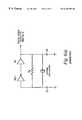
- a typical cable modemcontains an inexpensive, non-temperature-compensated crystal oscillator with an accuracy of 50-100 ppm as illustrated in FIG. 4 ( a ) which shows a typical standard crystal oscillator configured to output a digital clock output to be used by the rest of the cable modem's integrated circuitry.
- FIG. 4 ( b )A circuit designed to implement the VCXO approach of synchronization is illustrated in FIG. 4 ( b ).
- the element used in such a circuitis a voltage-variable capacitor—often implemented with a varactor diode such as diode D 1 of FIG. 4 ( b ). This circuit operates to vary the capacitance of capacitor C 1 and therefore the oscillating frequency of the Crystal Oscillator.
- successive timestamps from the headendare compared to time intervals from the local modem by the CPU 450 . If the local modem is running too fast, the frequency of the modem clock oscillator is reduced. Likewise, if the local clock is running too slow, the modem clock oscillator is increased. This can be done in one instance by providing digital signals from the CPU 450 to the Digital/Analog Converter 455 which in turn varies the voltage at the input of resistor R x in order to adjust the capacitance of C 1 and in turn adjust the Crystal Oscillators frequency.
- the present inventionprovides a method and apparatus for synchronizing the local clock of a transceiver in a communications system with the master clock of its corresponding communications system control unit such that some of the problems associated with currently known synchronization methods are avoided.
- a method of synchronizing the local clock of a transceiver with the master clock of a control unit to which the transceiver is coupledcomprises receiving a first timestamp with the transceiver, wherein the first timestamp comprises a signal generated by the control unit in response to the value of the master clock at the time the first timestamp signal is generated. Further, the method includes generating a first transceiver time reference with the transceiver device in response to the receipt of the first timestamp and generating a correction factor in response to the difference of the first timestamp and the first transceiver time reference.
- the methodincludes generating a synchronized downstream reference signal by adjusting an output clock signal of the local clock in response to the correction factor.
- the communications systemis a cable modem system in which the transceiver is a cable modem, and the control unit is a headend unit. Further, the steps of generating a correction factor and generating a synchronized downstream reference signal are performed by digital logic in one embodiment.
- the methodfurther comprises receiving a second timestamp with the transceiver, wherein the second timestamp comprises a signal generated by the control unit in response to the value of the master clock at the time the second timestamp signal is generated and generating a second transceiver time reference with the transceiver device in response to the receipt of the second timestamp.
- a control unit difference timeis then generated comprising the difference of the first and second timestamps.
- a transceiver difference timecomprising the difference of the first and second transceiver time references is also generated in addition to a clock error time wherein the clock error time comprises the difference of the control unit difference time and the transceiver difference time.
- the correction factor in this embodimentis generated in response to the clock error time.
- the first and second transceiver time referencescomprise time signals generated by the transceiver device in response to the values of the local clock at the times the first and second timestamps respectively are received.
- the correction factorcomprises an offset signal that corresponds to the clock error time divided by the transceiver difference time.
- the offset signalis representative of the local clock error per local clock pulse.
- correction factormay also comprise an addsub signal that indicates if the local clock is either running faster or slower than the master clock. Given the value of the addsub signal, the local clock output can be adjusted either upward or downward accordingly.
- the methodmay comprise the further step of generating a synchronized upstream reference signal.
- the synchronized upstream reference signalcomprises a time signal utilized by the transceiver to determine when the transceiver can transmit a first output signal to the control unit such that the first output signal does not collide with a second output signal transmitted by one or more other transceivers in the system that are connected to the control unit.
- the step of generating the upstream reference signalcomprises either adding or subtracting a delay offset time from the downstream reference signal.
- the delay offset timein this case comprises the amount of time required for a ranging time signal to be received by the transceiver after the ranging time signal is transmitted by the control unit.
- the inventionis described as a cable modem apparatus in a communications system comprising a headend unit including a master clock and a plurality of cable modems coupled to the headend unit.
- the cable modem apparatuscomprises an input/output node coupled to the headend unit and a receiver that is coupled to the input/output node and that receives a first timestamp generated by the headend unit in response to the value of the master clock at the time the first timestamp signal is generated.
- the cable modemalso includes a local clock configured to operate at substantially the same frequency as the master clock and a synchronization counter that is coupled to the receiver.
- the synchronization countergenerates a first cable modem time reference in response to the receipt of the first timestamp, and it also includes a correction signal generator that generates a correction factor in response to the difference of the first timestamp and the first cable modem time reference and a correction circuit that generates a synchronized downstream reference signal by adjusting an output clock signal of the local clock in response to the correction factor.
- the correction signal generator and the correction circuitmay comprise digital logic.
- the correction circuitalso generates a synchronized upstream reference signal.
- the synchronized upstream reference signalcomprises a time signal utilized by the cable modem to determine when the cable modem can transmit a first output signal to the headend unit such that the first output signal does not collide with a second output signal transmitted by a different cable modem in the system.
- the correction circuitgenerates the upstream reference signal by either adding or subtracting a delay offset time from the downstream reference signal.
- the delay offset timecomprises the amount of time required for a ranging time signal to be received by the cable modem after the ranging time signal is transmitted by the headend.
- the inventioncan be further characterized in that the receiver receives a second timestamp that is generated by the headend unit in response to the value of the master clock at the time the second timestamp signal is generated. Also, the synchronization counter generates a second cable modem time reference in response to the receipt of the second timestamp. Lastly, the correction signal generator generates the correction factor in response to the difference of a headend difference time and a cable modem difference time.
- the headend difference timecomprises the difference of the first and second timestamps
- the cable modem difference timecomprises the difference of the first and second cable modem time references.
- the first and second cable modem time referencescomprise a time signals generated by the cable modem in response to the values of the local clock at the times the first and second timestamps are respectively received.
- the correction factorcomprises an offset signal that corresponds to the clock error time divided by the transceiver difference time.
- the offset signalis representative of the local clock error per local clock pulse. In generating the synchronized downstream reference signal, this embodiment provides for adding the offset signal into an accumulator device on each pulse of the local clock and adjusting the output clock signal when the accumulator device rolls over.
- correction factormay also comprise an addsub signal that indicates if the local clock is either running faster or slower than the master clock. Given the value of the addsub signal, the local clock output can be adjusted either upward or downward accordingly.
- the present inventionmay also be characterized as an apparatus for synchronizing the local clock of a transceiver that is coupled to a control unit with the master clock of the control unit.
- the apparatuscomprises a means for receiving a first timestamp, wherein the first timestamp comprises a signal generated by the control unit in response to the value of the master clock at the time the first timestamp signal is generated.
- a means for generating a first transceiver time reference in response to the receipt of the first timestampa means for generating a correction factor in response to the difference of the first timestamp and the first transceiver time reference, and a means for generating a synchronized downstream reference signal that comprises an output clock signal of the local clock adjusted in response to the correction factor.
- the transceiver devicecomprises a cable modem and the control unit comprises a headend unit.
- the means for generating a correction factor and the means for generating a synchronized downstream reference signalcomprise digital logic.
- a further embodiment of this apparatusincludes a means for generating a synchronized upstream reference signal.
- the synchronized upstream reference signalcomprises a time signal utilized by the transceiver to determine when the transceiver can transmit a first output signal to the control unit such that the first output signal does not collide with a second output signal transmitted by another transceiver in the system.
- the generation of the upstream reference signalcomprises either adding or subtracting a delay offset time from the downstream reference time.
- the delay offset timein one case comprises the amount of time required for a ranging time signal to be received by the transceiver after the ranging time signal is transmitted by the control unit.
- the correction factoris generated in response to the value of a clock error time
- the apparatusalso includes a means for receiving a second timestamp, wherein the second timestamp comprises a signal generated by the control unit in response to the value of the master clock at the time the second timestamp is generated.
- Also included in this embodimentare a means for generating a second transceiver time reference in response to the receipt of the second timestamp, a means for generating a control unit difference time comprising the difference of the first and second timestamps, a means for generating a transceiver difference time comprising the difference of the first and second transceiver time references, and a means for generating the clock error time wherein the clock error time comprises the difference of the control unit difference time and the transceiver difference time.
- the correction factorcomprises an offset signal that corresponds to the clock error time divided by the transceiver difference time.
- the offset signalis representative of the local clock error per local clock pulse.
- this embodiment of the apparatusincludes a means for adding the offset signal into an accumulator device on each pulse of the local clock and a means for adjusting the output clock signal when the accumulator device rolls over.
- the correction factormay also comprise an addsub signal that indicates if the local clock is either running faster or slower than the master clock. Given the value of the addsub signal, the local clock output can be adjusted either upward or downward accordingly.
- FIG. 1illustrates, in simplified form, a typical downstream datastream from the headend of a typical cable modem system.
- FIG. 2illustrates, in block diagram form, a typical cable plant for a cable modem system.
- FIG. 3 ( a )illustrates, in simplified form, a typical upstream datastream to the headend of a typical cable modem system.
- FIG. 3 ( b )illustrates, in simplified form, a time chart displaying the relative times that a number of modems would have to send their data to the headend so as to arrive at the headend as illustrated in FIG. 3 ( a ).
- FIG. 4 ( a )illustrates, in schematic form, a typical standard crystal oscillator circuit used to generate a clock signal for a cable modem.
- FIG. 4 ( b )illustrates, in schematic form, the standard crystal oscillator circuit of FIG. 4 ( a ) modified by a voltage controlled oscillator circuit to allow for variable frequency control of the crystal oscillator.
- FIG. 5illustrates, in block diagram form, a typical cable modem in which one embodiment of the invention is utilized to synchronize the clock of the cable modem with the clock of the headend.
- FIG. 6illustrates one embodiment of a simplified logic circuit which can be utilized to provide a clock signal to a cable modem in accordance with the present invention.
- FIG. 7illustrates another embodiment of a simplified logic circuit which can be utilized to provide a clock signal to a cable modem in accordance with the present invention.
- FIG. 8illustrates still another embodiment of a simplified logic circuit which can be utilized to provide a clock signal to a cable modem in accordance with the present invention.
- FIGS. 9 ( a ), 9 ( b ), and 9 ( c )illustrate how the clock signal circuit of FIG. 8 can be utilized to provide faster and slower clock signals utilizing a number of different offset values.
- FIG. 10illustrates a simplified process flow diagram representing a method by which a cable modem clock signal can be synchronized in accordance with one embodiment of the invention.
- FIG. 11illustrates, in simple block diagram form, one embodiment of an apparatus which can perform the synchronization method of FIG. 10 .
- FIG. 12illustrates logic circuitry which may be used to implement one portion of the apparatus of FIG. 11 .
- FIG. 13illustrates further logic circuitry which may be used to implement other portions of the apparatus of FIG. 11 .
- the present inventionsynchronizes the clock of a local cable modem with that of the headend by following the basic method described below. Two successive timestamps are taken from the headend and compared to two local time samples from the local cable modem clock. These 4 measurements are used to compute an offset frequency that can be added or subtracted from the local clock to derive a new local clock frequency that is in perfect synchronization with the Headend. This is all done digitally, thus avoiding any non-idealities connected with analog hardware. Furthermore, no modification is required on the relatively inexpensive basic crystal oscillator typically used in cable modems.
- the basic conceptemploys an architecture based on a numerically-controlled oscillator (NCO), of the type employed in direct-digital synthesizers (DDS).
- NCOnumerically-controlled oscillator
- DDSdirect-digital synthesizers
- FIG. 5illustrates a block diagram of a two-way cable modem 500 that operates in accordance with one embodiment of the present invention.
- the cable modem 500is coupled to an external computer 580 , and includes a coaxial cable input/output 505 , a tuner 520 , a downstream demodulator 530 , an Ethernet network interface controller 535 , a custom ASIC Interface integrated circuit 550 , a local clock 560 , an upstream modulator 570 , a CPU 542 , a RAM 544 , and a ROM 546 .
- the tuner 520is comprised of a diplexer filter 522 including a high pass and low pass filter, and an up/down frequency converter 525 .
- the diplexer filter 522(highpass/lowpass) which is coupled to the input/output 505 of the modem 500 separates the low power, high frequency downstream signal coming from the headend 200 , from the high power, lower frequency upstream signal generated by the cable modem 500 itself.
- the downstream signalis a 64-QAM or 256-QAM signal in a frequency range of 54-850 MHz with a power level of between ⁇ 15 dBmV and +15 dBmV—the upstream signal covers a frequency range of 5-42 MHz with power levels ranging between +8 dBmV and +58 dBmV.
- the tuner 520is coupled to and receives modulated data from the upstream modulator 570 to be transmitted upstream to the headend 200 .
- This datapasses through the low pass filter of the diplexer filter 522 and is output through the coaxial cable input/output 505 .
- the cable modem 500receives modulated downstream input data from the cable headend 200 via the coaxial cable input/output 505 .
- This downstream input datapasses through the tuner 520 via the high pass filter of the diplexer filter 522 and then through the up/down converter 525 .
- the output of the up/down converter 525is received by the downstream demodulator 530 which demodulates the downstream input data.
- the custom ASIC Interface integrated circuit 550is coupled to the downstream demodulator 530 , the upstream modulator 570 , and the Ethernet network interface controller 535 such that data can be passed to and from these components. Further, the custom ASIC Interface integrated circuit 550 is coupled to the CPU 542 , the RAM 544 , and the ROM 546 through the internal modem bus 540 . The custom ASIC Interface integrated circuit 550 contains circuitry which, in conjunction with command signals generated by the CPU 542 , serves to control the overall operation of the cable modem 500 . The RAM 544 and the ROM 546 of the cable modem 500 serve to store, read, and write data to be utilized by the modem 500 , and to store operating instructions and configuration data for the modem 500 .
- the D/S signal processorreceives input from the D/S demodulator 530 , and performs a number of functions in response to this input.
- the D/S signal processor 553may pass on the raw data signal on to the rest of the ASIC 550 and it may also generate signals in response to the data received. For instance, in one embodiment, the D/S signal processor 553 may generate a number of logic level signals when it detects a timing type of signal from the headend 200 of the cable modem system.
- the synchronization counter 552operates in accordance with one embodiment of the present invention to synchronize the cable modem clock with the clock of the headend 200 .
- the synchronization counter 552receives input from a standard crystal oscillator circuit such as that shown in FIG. 4 ( a ) and also shown as local clock 560 , and from the D/S signal processor 553 , and corrects this clock output to match that of the headend 200 as will be described later in more detail with respect to FIGS. 10-13.
- the cable modem 500is coupled to an external computer 580 such as a personal desktop computer via the ethernet network interface controller 535 .
- the custom ASIC Interface integrated circuit 550may interface with the computer 580 through the ethernet network interface controller 535 when it is time to send data to the headend 200 of the cable modem system. This data can then be sent from a typical storage medium in the computer 580 (such as from a RAM, a ROM, an EEPROM, a floppy disk drive, or a CDROM) and into the custom ASIC Interface integrated circuit 550 where it is then passed to the upstream modulator 570 and the low pass filter of the diplexer filter 522 before being transmitted to the cable system headend 200 via the coaxial cable input/output 505 .
- a typical storage medium in the computer 580such as from a RAM, a ROM, an EEPROM, a floppy disk drive, or a CDROM
- demodulated downstream input data from the downstream demodulator 530may be sent to the computer 580 via the custom ASIC Interface integrated circuit 550 and the ethernet network interface controller 535 .
- This demodulated downstream input datamay then be stored and/or utilized by the computer 580 to perform a number of computing operations in accordance with software programs being run on the computer 580 .
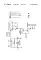
- FIG. 6illustrates a circuit which displays one known method in which a clock reference may be built.
- This circuitsimply comprises a counter 600 which is incremented in a binary fashion each time a rising edge of clock 605 comes along.
- the clock 605is shown as the output of buffer B 1 of the standard crystal oscillator circuit of FIG. 4 ( b ).
- the counteris a 3-bit binary counter. The maximum count is dictated by the number of bits in the counter (which is 111 binary or 7, in this example). When the count reaches its maximum value, it will roll over to a count of zero on the next rising edge.
- a digital comparator 610we can use a digital comparator 610 to tell a CPU associated with a cable modem (such as the CPU 542 of FIG.
- FIG. 7illustrates a circuit embodying an alternative way to provide a reference clock.
- the standard binary counter of FIG. 6is replaced with an N-bit accumulator 700 .
- the accumulator 700is shown as a 3-bit accumulator.
- the accumulator 700 outputis fed back to one of the adder 710 inputs, so that on the next positive edge of the clock 720 , a new value is latched on the output.
- the clock 720is, as was the case in FIG. 6, the output of buffer B 1 of the standard crystal oscillator circuit of FIG. 4 ( b ). If the offset added is always 1, then the count will increment by one each time just as it did with the standard binary counter of FIG. 6 . As expected, the count rolls over once it reaches 111 binary or 7.
- DDSdirect digital synthesizer
- FIG. 8A new way to change the frequency is shown in FIG. 8 .
- the circuit of FIG. 8is a numerically controlled oscillator (NCO) comprising a 5-bit accumulator 800 , an adder 810 , an offset 815 , a digital comparator 825 , and a threshold 830 .
- NCOnumerically controlled oscillator
- the circuitworks similar to the accumulator circuit of FIG. 7 with the following exceptions.
- the offset 815is a 5-bit offset wherein some bits are utilized such that they are effectively “behind a decimal point”, specifically 2 bits in this example. Only the 3 Most Significant Bits (MSB's) are fed from the accumulator 800 to other parts of the system such as the digital comparator 825 . The 2 bits below the decimal point are only used for internal calculations within the accumulator 800 . If one adds slightly more than one, say an offset 815 of 001.01 to the count on each clock 820 edge, the NCO will cycle through its maximum count in less clock cycles than if one were to add an offset 815 of 001.00 on each clock 820 edge. Similarly, one can make the NCO cycle through its maximum count more slowly by adding in an offset slightly less than one on each clock cycle.
- MSB's3 Most Significant Bits
- FIGS. 9 ( a )-( c )The action of the NCO with various offsets is shown in FIGS. 9 ( a )-( c ).
- the offsetis 001.00 and the output of the accumulator 800 passes the threshold 830 on the 6th clock edge.
- FIG. 9 ( b )the offset is slightly higher than that of FIG. 9 ( a ) at 001.01 and the output of the accumulator 800 passes the threshold 830 more quickly—on the 5th clock edge.
- FIG. 9 ( c )the offset is slightly lower that of FIG. 9 ( a ) at 000.11 and the output of the accumulator 800 passes the threshold 830 more slowly—on the 8th clock edge.
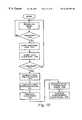
- a version of the NCO concept described above with respect to FIGS. 8-9is utilized to create a synchronization counter 552 that mirrors the time synchronization counter in the headend 200 of the cable modem system.
- Thisis illustrated by the process flow diagram of FIG. 10 .
- a headend signalis received by the cable modem 500 from the headend 200 .
- the headend signalis received by the D/S signal processor 553 via the D/D demodulator 530 and analyzed to detect any timing signals as shown by decision block 1005 .
- the cable modem 500Upon detecting a timestamp signal, the cable modem 500 stores the timestamp data 1007 and the local clock data 1009 corresponding to the time the timestamp is received.
- a timestamp signalis broadcast to the cable modem system by the headend 200 at an interval of from 200-600 milliseconds.
- decision block 1010if only one timestamp signal had been received by the cable modem 500 since a certain event such as power on or a reset, then the cable modem 500 continues to wait for a second timestamp signal from the headend 200 .
- a headend time difference(heTimeDiff) is computed by subtracting the received timestamps stored at block 1007 as shown at block 1015 .
- a cable modem difference (cmTimeDiff)is computed by counting the clocks between the timestamps, which in one embodiment is performed by taking the difference in the local clock data stored at block 1009 .
- a clock erroris generated.
- the difference between the cmTimeDiff and heTimeDiffis the clock error (clkErr).
- the clkerrrepresents the number of clocks that the headend 200 clock is ahead or behind the local clock of the cable modem 500 .
- the local clock of the cable modemis a 10.248 mhz clock such as that illustrated in FIG. 4 ( a ).
- a correction signalis then generated.
- the correction signalis generated by dividing the clkerr by the cmTimeDiff.
- the correction signalincludes an Offset signal and an AddSub signal, and in one embodiment is a 24 bit signal.
- the Offset signalrepresents the clock difference per clock, and the AddSub signal represents whether the local clock of the modem 500 is faster or slower than the headend 200 clock.
- the Offset signalin one embodiment, can be averaged over time to gain a stable Offset signal that removes small amounts of jitter and noise from the signal.
- the synchronization counter 532 of the cable modem 500generates a synchronized clock signal by utilizing the generated correction signal. In one embodiment, this is performed by adding the Offset value into an accumulator on every 10.248 mhz clock. Thus, when the accumulator rolls over, a single clock of difference exists between the modem 500 and the headend 200 .
- This clock of errorcan then be removed from the modem's time synchronization counter 552 by skipping or it can be added by incrementing the count by 2—the determination whether to skip or increment by 2 is decided by the value of the AddSub portion of the correction signal which, as stated previously, indicates whether the local clock is faster or slower than the headend 200 clock.
- the time synchronization counter 552should never be off by more than a clock, and the accumulating inaccuracy of the correction signal itself.
- the timestamp intervalis 600 milliseconds and the size of the correction signal is 24 bits
- the correction signalis large enough such that the accumulated error in the correction signal over 600 ms is less than a clock.
- a digital filtercould be used to average, or filter, successive timestamps obtained from the headend 200 .
- Such filteringwould greatly reduce any inherent jitter contained in the headend timestamps, such as would be due to MPEG synchronization. While such digital filtering would also mean that more timestamp values would need to be taken, considerable reduction of jitter might be achieved at the price of only a few seconds of real time. In most applications, clock acquisition times on the order of a second or two would generally be tolerable.
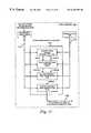
- FIG. 11illustrates, in simple block diagram form, one embodiment of an apparatus which can perform the synchronization method described above with respect to FIG. 10 .
- This apparatuscomprises the synchronization counter 552 which receives input from the D/S signal processor 553 and from the local clock 560 , all of which are included in a cable modem 500 as described previously with respect to FIG. 5 .
- the synchronization counter 552comprises a correction signal generator 1105 , an NCO correction circuit 1110 , a D/S reference time generator 1115 , and an U/S reference time generator 1120 , each of which receive input from both the D/S signal processor 553 on line 1102 and the local clock 560 on line 1104 .
- the correction signal generator 1105 , NCO correction circuit 1110 , D/S reference time generator 1115 , and the U/S reference time generator 1120are implemented by digital logic circuit elements on an integrated circuit—these digital logic circuit elements include such common elements as AND, NAND, OR, NOR, XOR, XNOR, NOT, buffers, Adders, Half-Adders, Comparators, Flip-Flops, Counters, and Shift Registers among others. Fuller descriptions of how these logic elements work and how they are implemented in the design of digital logic circuits can be found in a number of electrical engineering textbooks. Among others, these references include the following which are hereby incorporated by reference herein: L EONARD S. B OBROW , Fundamentals of Electrical Engineering , Ch.
- each of the correction signal generator 1105 , NCO correction circuit 1110 , D/S reference time generator 1115 , and the U/S reference time generator 1120are provided on the same integrated circuit.
- the digital logic elementsoperate using the local clock 560 signal as their common clock timing signal.
- the correction signal generator 1105receives information from the D/S signal processor 553 on line 1102 and the local clock 560 signal on line 1104 .
- the information on line 1102may include timestamp information and other signals produced by the D/S signal processor 553 in response to the receipt of timing signals from the headend 200 .
- These other signalsmay include, in one embodiment, pulsed logic level signals such as LoadTimeSync and syncFound, and digital data such as mmpMSGData all of which will be described in more detail with respect to FIGS. 12 and 13.
- the correction signal generator 1105generates the correction signal described above with respect to FIG. 10 comprising the Offset and the AddSub signals, and provides the Offset and AddSub signals to the NCO correction circuit 1110 .
- the NCO correction circuit 1110receives the Offset and Add Sub signals, information from the D/S signal processor 553 on line 1102 and the local clock 560 signal on line 1104 .
- the NCO correction circuit 1110operates using an accumulator as described with respect to FIG. 10 to add the Offset signal to an adder on every local clock pulse. When the accumulator rolls over, the NCO correction circuit generates a digital high Carryout signal and provides this signal to the D/S reference time generator 1115 along with the AddSub signal.
- the D/S reference time generator 1115utilizes this information, along with information from the D/S signal processor 553 on line 1102 , and the local clock 560 signal on line 1104 to generate the D/S reference time DSRef as will be described in further detail with respect to FIG.
- the DSRef signalwhen the Carryout signal is low the DSRef signal comprises a signal that counts forward +1 with each pulse of the local clock 560 .
- the accumulator of the NCO correction circuit 1110 rolls over the Carryout signalgoes high and the DSRef signal is corrected in accordance with the value of the AddSub signal. If the AddSub signal is high, the DSRef signal is adjusted upwards +2 on the current local clock 560 signal—if the AddSub signal is low, the DSRef signal is not adjusted at all on the current local clock 560 signal, it skips a forward count in order to adjust back to the headend 200 clock.
- one embodiment of the inventionis designed such that the DSRef signal is equal to a clock signal that should never be off by more than a clock, and the accumulating inaccuracy of the correction signal itself.
- the DSRef signalis then provided to the U/S reference time generator 1120 .
- the U/S reference time generator 1120uses this information to generate an USRef time that is provided to the CPU 542 and/or the U/S modulator 570 on line 1106 such that the modem 500 can accurately calculate its designated minislot times for transmitting upstream data on the cable modem system such that it does not collide with upstream data from other cable modems in the system.
- the USRef timeis a time utilized by the modem 500 to determine when a particular minislot begins and ends.
- the USRefis a 32 bit value in which the number of bits which represent a minislot is determined by the number of clocks in a minislot.
- the USRefis a programmable delay offset from the DSRef
- the value of this delay offsetis programmed into the modem 500 in one embodiment by a ranging procedure performed between the headend 200 and the modem 500 at modem 500 initial power up.
- the ranging procedurein one embodiment consists of a procedure in which the headend 200 sends a calibrating signal out to determine how long it takes information to travel to a particular modem 500 as described previously above in the background section.
- This ranging procedurecan also be performed by the headend 200 on particular modems in the system at various scheduled times during modem 500 operation so that the delay offset value may change during modem 500 operation.
- the delay offset determined by the ranging procedureis, in one embodiment, added to the DSRef signal to generate the USRef time.
- the CPU 542can direct a data transmission through the U/S modulator 570 to the headend 200 . Since the DSRef signal is corrected to within one clock of the headend 200 clock, the data should reach the headend 200 within the designated minislot and should never be off by more than one clock plus any accumulated error in the correction signal, and any error in the value of the range time.
- the operation of the D/S reference generator 1120is described below more specifically with respect to FIG. 13 .
- FIG. 12illustrates logic circuitry which may be used to implement the correction signal generator 1105 .
- the correction signal generator 1105comprises oldTimeSync register 1205 , difference logic element 1210 , heTimeDiff register 1215 , difference logic element 1220 , TimeAlu divider logic element 1225 , cmTimeDiff register 1230 , local counter register 1240 , +1 adder logic element 1235 , difference logic element 1260 , and local counter reset logic element 1250 .
- the D/S signal processor 553which receives D/S data from the headend 200 via the D/S demodulator 530 .
- the D/S signal processorWhen a timing type signal (timestamp) is detected from the headend 200 , the D/S signal processor, in one embodiment, generates a digital high LoadTimeSync signal on line 1201 , a digital high syncFound signal on line 1203 , and signal mmpMSGData on line 1202 which consists of the actual headend timestamp value.
- the oldTimeSync registerreceives its input from line 1202 , and is activated by a Load signal from line 1201 .
- the output of the oldTimeSync register 1205is provided as an input to the difference logic element 1210 .
- the difference logic element 1210also receives an input from line 1202 , and the output of the difference element 1210 is provided to the heTimeDiff register 1215 .
- the heTimeDiff register 1215is activated by a Load signal from line 1201 , and the output of the heTimeDiff register 1215 —which as described earlier with respect to FIG. 10 represents the time difference between successive timestamps—is provided to difference logic element 1220 .
- cmTimeDiff register 1230which receives its input from local counter register 1240 and is activated by a Load signal on line 1203 —is also provided to the difference logic element 1220 . As stated with respect to FIG. 10, in one embodiment of the invention, the output of cmTimeDiff register 1230 is equal to the time which the cable modem local clock has counted between timestamps.
- the output of difference logic element 1220comprises data representing the difference between the heTimeDiff output and the cmTimeDiff output and has two portions designated by the bit positions of the data.
- one bit of the output of the difference logic element 1220represents whether the cmTimeDiff is greater than or less than the heTimeDiff—this is shown as signal newAddSub.
- the newAddSub bitis a digital low or 0, and when the local clock is running slower than the headend 200 clock and the cmTimeDiff is correspondingly less than the heTimeDiff, the newAddSub bit is a digital high or 1.
- the remainder of the output of the difference logic 1220represents the absolute difference between the cmTimeDiff and the heTimeDiff signals, and in one embodiment is a 24 bit signal.
- This absolute difference portion of the outputis provided as an input to TimeAlu divider logic element 1225 .
- Also provided as an input to the TimeAlu divider logic 1225is the output of cmTimeDiff register 1230 .
- the TimeAlu divider logic 1225acts to divide the absolute difference by the cmTimeDiff and generate an output newOffset on line 1224 wherein the newOffset signal represents the local clock difference per clock as described above with respect to FIG. 10 .
- the overall output of the correction signal generator 1105is a correction signal which comprises both the newAddSub signal on line 1222 and the newOffset signal on line 1224 .
- the remainder of the elements of the correction signal generator 1105are designed to provide for a new count of the local clock between each set of received timestamps.
- the difference logic element 1260receives one input from the output of the cmTimeDiff register 1230 and another input from the output of the +1 adder logic element 1235 .
- the output of the difference logic element 1260is provided to input R (Reset) of the local counter reset logic element 1250 .
- the C (Count) input of the local counter reset logic element 1250is provided by the output of the +1 adder logic element 1235 , and the local counter reset logic element 1250 is activated by a Load signal on line 1203 .
- the output of the local counter reset logic element 1250is provided to the input of the local counter register 1240 .
- the output of the local counter register 1240is provided to the input of the cmTimeDiff register 1230 and also to the input of the +1 adder logic element 1235 .
- the logic elements of the embodiment of the correction signal generator 1105 illustrated in FIG. 12operate as follows upon the receipt of a timestamp signal from the headend 200 by the D/S signal processor.
- the syncFound signalis pulsed high thereby activating the cmTimeDiff register 1230 , and the current value of the cmTimeDiff register 1230 is provided to the difference logic 1220 and the TimeAlu divider logic 1225 .
- the output of the cmTimeDiff register 1230is also provided to difference logic 1260 along with the output of +1 adder logic 1235 .
- the output of the difference logic 1260serves to then reset the local counter register 1240 to prepare for the next timestamp.
- the pulsed high syncFound signalactivates the local counter reset logic element 1250 and the input at R is then provided to the local counter 1240 .
- the value of the local counter register 1240is provided by input C of the local counter reset logic element 1250 , which in turn is provided by the output of the +1 adder logic 1235 .
- the +1 adder logic 1235receives an input from local clock 560 and serves to count up the value of the local counter 1240 upon each leading edge of the local clock 560 by a value of 1 clock. In this manner, the output of cmTimeDiff register 1230 always equals the true local clock time difference for a particular corresponding set of timestamps.
- the LoadTimeSync signalis pulsed high thereby activating both the oldTimeSync register 1205 and the heTimeDiff register 1215 .
- the mmpMSGData signalrepresenting the timestamp data is transmitted on line 1202 and latched into oldTimeSync register 1205 .
- the old timestamp data from the previous timestamp which was resident in the oldTimeSync register 1205is provided to difference logic 1210 along with the mmpMSGData and the difference between the old and new timestamps (heTimeDiff) is generated and latched into heTimeDiff register 1215 whose output is provided to one of the inputs of difference logic 1220 .
- a new correction signal for the latest timestampis now generated as described above.
- FIG. 13illustrates one embodiment of logic circuitry which may be used to implement the NCO correction circuit 1110 , the D/S reference time generator 1115 , and the U/S reference time generator 1120 of the synchronization counter 552 of FIG. 11 . Also shown is D/S signal processor 553 which provides signals LoadTimeSync, mmpMSGData, and syncFound on lines 1201 , 1202 , and 1203 respectively as described previously. Similarly, correction signal generator 1105 is also shown as a provider of outputs newOffset and newAddSub on lines 1224 and 1222 respectively.
- One embodiment of the NCO correction circuit 1110comprises offset register 1355 , adder logic element 1360 , accumulator logic element 1365 , offset register reset logic element 1350 , difference logic element 1375 , threshold register 1370 , comparator logic element 1380 , and AND gate 1385 .
- the offset register reset logic element 1350receives inputs newAddSub and newOffset on lines 1222 and 1224 respectively from the correction signal generator 11 05 .
- the input to the Load(which is provided by the output of AND gate 1385 ) of offset register reset logic element 1350 is pulsed high the current contents of the offset register reset logic element 1350 are latched into the offset register 1355 .
- the offset register 1355stores information which comprises the current Offset and AddSub being used by the modem 500 to synchronize its local clock 560 with the clock of the headend 200 by correcting the DSRef time and the USRef time as discussed earlier.
- the offset register 1355provides the Offset signal (which in one embodiment is a 24 bit signal) as an input to the adder logic element 1360 and to the difference logic element 1375 , and provides the AddSub signal as an input to the DSRef logic 1325 of the D/S reference time generator 1115 .
- the adder logic element 1360receives a second input signal from the accumulator logic element 1365 , and the adder 1360 provides its output as an input to the accumulator logic element 1365 .
- the Offset signalis generated such that it approximately equals the clock difference between the local clock 560 and the headend 200 clock per cable modem clock.
- the Offset signalis added to the current value of the accumulator 1365 in the adder 1360 and provided to the accumulator 1365 . In this manner, the accumulator 1365 should roll over at a time at which the local clock 560 is no more than one clock ahead or behind the headend 200 clock from the time of the last roll over.
- the accumulator 1365rolls over and generates a high Carryout signal to the DSRef logic 1325 to make a synchronization correction to the DSRef 1315 time, it does so at a time such that the DSRef time 1315 (and correspondingly the USRef 1340 time) is never more than a clock from the headend 200 time.
- the newOffset signal on line 1224is also provided as an input to the difference logic element 1375 , and the output of the difference logic 1375 is provided as an input to comparator logic 1380 along with the value of threshold register 1370 .
- the output of the comparator logic 1380is provided as an input to the AND gate 1385 .
- the second input of the AND gateis provided by a signal from the CPU 542 . In this manner, as discussed briefly above, the output of the AND gate 1385 can be controlled such that it is high (and therefore the newOffset signal is latched into the offset register 1355 to be used as the current Offset signal) only when certain predefined or variable conditions are met.
- the output of the comparator 1380is low and the output of the AND gate is low thereby disabling any latching of the newOffset into the offset register 1355 .
- the value of the threshold register 1370could be any user or system designated value which serves to ensure consistent modem 500 performance.
- the cable modem 500could generate an interrupt signal which disables the modem 500 from transmitting upstream data until some designated event such as a system time calibration is performed satisfactorily.
- the second input of the AND gate 1385can be used to dynamically or statically control when the newOffset is to be latched into the offset register 1355 .
- software operating within a computer to which the cable modem 500 is attachedmay control the process such that the newOffset is latched at predetermined time intervals such as every 10th timestamp, or any other interval. In another instance, this interval may be determined randomly within some range of timestamp intervals. In still another instance, the designation of the timestamp interval to be used may be chosen by the user interfacing with the software program.
- the CPU 542may provide a high pulsed signal on the second input of the AND gate 1385 dynamically in accordance with the performance of the cable modem 500 .
- the output of difference logic 1320which as will be described later is equal to the difference in time (DSRefDiff) between a headend timestamp and the corrected DSRef time of the modem 500 —exceeds some static or adjustable threshold thereby indicating the current Offset signal is not adequately correcting the DSRef time
- the CPUmay pulse its output to the AND gate 1385 in order to latch the newOffset into the offset register 1355 in an attempt to refine the DSReftime 1315 .
- the D/S reference time generator 1115comprises oldTimeSync register 1305 , SyncDSRef register 1310 , DSRef register 1315 , difference logic element 1320 , and DSRef logic element 1325 .
- the DSRef register 1315provides the current DSRef time of the modem 500 which as described previously, is the modem's corrected or synchronized time signal.
- the DSRef register 1315receives its input from the output of the DSRef logic 1325 , and is updated on each clock signal of the local clock 560 in accordance with the operation of the DSRef logic 1325 .
- the DSRef logic 1325receives inputs from the difference logic 1320 , the DSRef register 1315 , and the AddSub and Carryout signals discussed above with respect to the NCO correction circuit 1110 .
- the difference logic 1320receives inputs from the oldTimeSync register 1305 and the SyncDSRef register 1310 .
- the oldTimeSync register 1305is activated by a high LoadTimeSync signal on line 1201 which is generated as described previously with respect to FIG. 12 —and receives timestamp data as its input on line 1202 in the form of signal mmpMSGData from the D/S signal processor 553 .
- the SyncDSRef register 1310is activated by a high syncFound signal on line 1203 as described above with respect to FIG. 12 —and receives the current DSRef time as its input from DSRef register 1315 .
- the embodiment of the D/S reference time generator 1115 illustrated in FIG. 13operates as follows to generate the modem's 500 synchronized downstream time signal DSRef Generally, in one embodiment, the D/S reference time generator 1115 operates to generate a DSRef time that is an incrementing 10.248 MHz counter that is adjusted by new timestamps when they are received and adjusted continuously by the correction signal (Offset and AddSub) that is generated by the correction signal generator 1105 and applied by the NCO correction circuit 1110 . More specifically, in the embodiment illustrated in FIG. 13, the DSRef logic 1325 , on each clock cycle of the local clock, steps through the logic enumerated within block 1325 of FIG. 13 .
- the DSRef logic 1325updates the value of DSRef in the DSRef register 1315 by setting it equal to the value of the previous DSRef time plus the DSRefDiff (which is equal to the output of difference logic 1320 ) plus 1 clock cycle.
- the ldDSRef signalis high when the modem 500 receives a timestamp from the headend 200 , and the difference between the timestamp data latched into the oldTimeSync register 1305 upon receipt of a timing signal is within some designated threshold of the value of the DSRef time latched into the SyncD SRef register 1310 when the timestamp is received.
- the DSRefDiff output of difference logic 1320is greater than this threshold—which for instance might be set at 16 clocks in one embodiment—then the DSRef time should be construed as invalid and the upstream channel of the modem 500 is shut down to be resynchronized. Since the difference logic 1320 is comparing the value of a timestamp with the value of the modem's corrected time DSRef, then the difference DSRefDiff should be relatively small. If it is not small it would be an indication of a synchronization problem.
- the DSRef logic 1325determines if both the Carryout and the AddSub signals are high. If they are not both high, the DSRef logic 1325 proceeds to the next step. If they are both high the DSRef logic 1325 updates the value of the DSRef register 1315 by setting it equal to the value of the previous DSRef plus two clocks. As noted earlier, when the Carryout is high it is an indication that the accumulator 1365 has rolled over and therefore that the local clock has deviated from the value of the headend clock by a single clock since the last roll over.
- the DSRef register 1315up or down whenever Carryout is high, the DSRef time should never be more than a single clock off from the headend 200 time. In this case, the clock is adjusted ahead two clocks because the high AddSub signal is an indication that the local clock is slower than the headend 200 clock.
- step three of the DSRef logic 1325if Carryout is high (and AddSub is low) then the DSRef register is not advanced any clocks for that particular clock cycle. This serves to bring the DSRef time back to the headend 200 time since the low AddSub signal indicates that the local clock is faster than the headend 200 .
- the DSRef logic 1325updates the DSRef register 1315 by a single clock.
- the embodiment of the U/S reference time generator 1120 illustrated in FIG. 13comprises an adder 1330 , a range register 1335 , and an USRef register 1340 .
- the adder 1330receives inputs from the DSRef register 1315 and the range register 1335 , and provides output to the input of the USRef register 1340 .
- the USRef register 1340provides a synchronized time signal USRef with a delay offset to the CPU 542 and/or the U/S modulator 570 .
- This USRef timeis utilized to determine when the modem 500 can transmit upstream data such that it arrives at the headend 200 within that particular modem's designated mini timeslot such that it does not collide with upstream transmissions from other modem's in the system.
- the delay offsetis determined by the value of the range register 1335 which, in one embodiment, holds a value representing the time which it takes a signal transmitted from that particular modem to reach the headend 200 .
- the range valueis set by a ranging procedure performed between the headend 200 and the modem 500 at the power on of the modem. In other embodiments, this ranging procedure could be performed at set or random times throughout the operation of the modem in addition to the original power on ranging.
Landscapes
- Engineering & Computer Science (AREA)
- Computer Networks & Wireless Communication (AREA)
- Signal Processing (AREA)
- Synchronisation In Digital Transmission Systems (AREA)
Abstract
Description
Claims (54)
Priority Applications (1)
| Application Number | Priority Date | Filing Date | Title |
|---|---|---|---|
| US09/199,030US6449291B1 (en) | 1998-11-24 | 1998-11-24 | Method and apparatus for time synchronization in a communication system |
Applications Claiming Priority (1)
| Application Number | Priority Date | Filing Date | Title |
|---|---|---|---|
| US09/199,030US6449291B1 (en) | 1998-11-24 | 1998-11-24 | Method and apparatus for time synchronization in a communication system |
Publications (1)
| Publication Number | Publication Date |
|---|---|
| US6449291B1true US6449291B1 (en) | 2002-09-10 |
Family
ID=22735916
Family Applications (1)
| Application Number | Title | Priority Date | Filing Date |
|---|---|---|---|
| US09/199,030Expired - Fee RelatedUS6449291B1 (en) | 1998-11-24 | 1998-11-24 | Method and apparatus for time synchronization in a communication system |
Country Status (1)
| Country | Link |
|---|---|
| US (1) | US6449291B1 (en) |
Cited By (119)
| Publication number | Priority date | Publication date | Assignee | Title |
|---|---|---|---|---|
| US20010016024A1 (en)* | 2000-01-26 | 2001-08-23 | Thomas Treyer | Configuration and method for clock regeneration |
| US20010046289A1 (en)* | 2000-04-07 | 2001-11-29 | Robinson Timothy B. | Method and apparatus for transceiver noise reduction in a frame-based communications network |
| US20030014763A1 (en)* | 2001-06-29 | 2003-01-16 | Chappell Christopher L. | Method and apparatus facilitating synchronization in a broadband communications system |
| US20030056136A1 (en)* | 2001-09-18 | 2003-03-20 | James Aweya | Technique for synchronizing clocks in a network |
| US20030058893A1 (en)* | 2001-09-27 | 2003-03-27 | Broadcom Corporation | Synchronization of multiple cable modem termination systems |
| US20030117899A1 (en)* | 2001-12-24 | 2003-06-26 | Eidson John C. | Distributed system time synchronization including a timing signal path |
| US6611868B1 (en) | 1999-05-21 | 2003-08-26 | 3Com Corporation | Method and system for automatic link hang up |
| US6618815B1 (en)* | 2000-02-29 | 2003-09-09 | International Business Machines Corporation | Accurate distributed system time of day |
| US20030174734A1 (en)* | 2002-02-22 | 2003-09-18 | Matthew Compton | Frequency synchronisation of clocks |
| US6633862B2 (en)* | 2000-12-29 | 2003-10-14 | Intel Corporation | System and method for database cache synchronization across multiple interpreted code engines |
| US6636485B1 (en) | 1998-05-14 | 2003-10-21 | 3Com Corporation | Method and system for providing quality-of-service in a data-over-cable system |
| US20030214982A1 (en)* | 2002-05-17 | 2003-11-20 | Broadcom Corporation | Method and circuit for insertion of time stamp into real time data |
| US6661811B1 (en)* | 1999-02-12 | 2003-12-09 | Koninklijke Philips Electronics N.V. | Method of and apparatus for communicating isochronous data |
| US6698022B1 (en)* | 1999-12-15 | 2004-02-24 | Fujitsu Limited | Timestamp-based timing recovery for cable modem media access controller |
| US20040090994A1 (en)* | 2000-07-20 | 2004-05-13 | Lockridge Terry Wayne | Multi-media jitter removal in an asynchronous digital home network |
| US20040093435A1 (en)* | 2001-03-29 | 2004-05-13 | Juha Purho | Method for synchronizing a first clock to a second clock, processing unit and synchronization system |
| US6747983B1 (en)* | 1998-10-02 | 2004-06-08 | Thomson Licensing S.A. | Transport packet rate conversion |
| US6751228B1 (en)* | 1999-03-23 | 2004-06-15 | Yamaha Corporation | Packet handler of audio data by isochronous mode |
| US6754622B1 (en) | 1999-05-24 | 2004-06-22 | 3Com Corporation | Method for network address table maintenance in a data-over-cable system using destination reachibility |
| US6760798B1 (en)* | 2000-07-13 | 2004-07-06 | Arm Limited | Interface mechanism and method for interfacing a real-time clock with a data processing circuit |
| US6763274B1 (en)* | 1998-12-18 | 2004-07-13 | Placeware, Incorporated | Digital audio compensation |
| US20040141526A1 (en)* | 2003-01-16 | 2004-07-22 | Sivaram Balasubramanian | Fast frequency adjustment method for synchronizing network clocks |
| US6775276B1 (en) | 1998-05-27 | 2004-08-10 | 3Com Corporation | Method and system for seamless address allocation in a data-over-cable system |
| US6785292B1 (en) | 1999-05-28 | 2004-08-31 | 3Com Corporation | Method for detecting radio frequency impairments in a data-over-cable system |
| US20040190487A1 (en)* | 2003-03-31 | 2004-09-30 | Biggs Robert A. | Method for synchronizing a control channel to a working channel |
| US6804262B1 (en) | 2000-04-28 | 2004-10-12 | 3Com Corporation | Method and apparatus for channel determination through power measurements |
| US20040202203A1 (en)* | 2003-04-09 | 2004-10-14 | Broadcom Corporation | Method and apparatus for maintaining synchronization in a communication system |
| US20040202202A1 (en)* | 2003-04-09 | 2004-10-14 | Broadcom Corporation | Method and apparatus for maintaining synchronization in a communication system |
| US6807195B1 (en)* | 1999-09-29 | 2004-10-19 | General Instrument Corp. | Synchronization arrangement for packet cable telephony modem |
| US6816492B1 (en)* | 2000-07-31 | 2004-11-09 | Cisco Technology, Inc. | Resequencing packets at output ports without errors using packet timestamps and timestamp floors |
| US6816500B1 (en) | 2000-07-10 | 2004-11-09 | 3Com Corporation | Apparatus, method and system for multimedia access network channel management |
| US20040252678A1 (en)* | 1999-02-12 | 2004-12-16 | Broadcom Corporation | Cable modem system with sample and packet synchronization |
| FR2856162A1 (en)* | 2003-06-13 | 2004-12-17 | Eads Deutschland Gmbh | Clocks synchronizing method for use in microprocessor system, involves adjusting cycle period of one of two clocks using adjustment factor determined from modification of position of clock flanks, to reduce time deviation between clocks |
| US20050033862A1 (en)* | 2001-11-28 | 2005-02-10 | Philipp Blum | Method for syncronization in networks |
| US6876670B1 (en)* | 1998-05-19 | 2005-04-05 | Curtin University Of Technology | Method and apparatus for transfer of real time signals over packet networks |
| US6886180B1 (en)* | 2000-08-16 | 2005-04-26 | Intel Corporation | Implementing cable modem functions on a host computer |
| US6892229B1 (en) | 1998-09-30 | 2005-05-10 | 3Com Corporation | System and method for assigning dynamic host configuration protocol parameters in devices using resident network interfaces |
| US6940874B2 (en) | 2000-11-30 | 2005-09-06 | 3Com Corporation | Method for reducing interference from initializing network devices in a data-over-cable system |
| US6944881B1 (en) | 2000-06-19 | 2005-09-13 | 3Com Corporation | Method for using an initial maintenance opportunity for non-contention ranging |
| US6948184B1 (en) | 2000-11-30 | 2005-09-20 | 3Com Corporation | System and method for calibrating power level during initial ranging of a network client device |
| US20050254615A1 (en)* | 2004-05-12 | 2005-11-17 | Richard Bourdeau | Apparatus and method for a programmable clock generator |
| US6975652B1 (en)* | 2000-10-18 | 2005-12-13 | 3Com Corporation | Clock synchronization of HFC telephone equipment |
| US6985437B1 (en) | 1999-05-25 | 2006-01-10 | 3Com Corporation | Method for dynamic performance optimization in a data-over-cable system |
| US6986157B1 (en) | 1998-12-21 | 2006-01-10 | 3Com Corporation | Method and system for dynamic service registration in a data-over-cable system |
| US20060013263A1 (en)* | 2004-07-19 | 2006-01-19 | Fellman Ronald D | System and method for clock synchronization over packet-switched networks |
| US20060036769A1 (en)* | 2004-04-30 | 2006-02-16 | Frey Robert T | Storage switch task processing synchronization |
| US7068597B1 (en) | 2000-11-27 | 2006-06-27 | 3Com Corporation | System and method for automatic load balancing in a data-over-cable network |
| US7073055B1 (en) | 2001-02-22 | 2006-07-04 | 3Com Corporation | System and method for providing distributed and dynamic network services for remote access server users |
| US7073190B1 (en)* | 1999-05-04 | 2006-07-04 | Two Way Media Limited | Interactive applications |
| US7072337B1 (en) | 2002-01-25 | 2006-07-04 | 3Com Corporation | System and method for resolving network addresses for network devices on distributed network subnets |
| US7085306B1 (en) | 2001-10-30 | 2006-08-01 | 3Com Corporation | System and method for a multi-frequency upstream channel in a computer network |
| US7088678B1 (en) | 2001-08-27 | 2006-08-08 | 3Com Corporation | System and method for traffic shaping based on generalized congestion and flow control |
| US7089580B1 (en)* | 2000-03-29 | 2006-08-08 | 3Com Corporation | Method for improved cable modem ranging in a data-over-cable system |
| US20060182148A1 (en)* | 1998-10-30 | 2006-08-17 | Broadcom Corporation | Method and apparatus for the synchronization of multiple cable modern termination system devices |
| US7099338B1 (en) | 1999-02-27 | 2006-08-29 | 3Com Corporation | System and method for insuring dynamic host configuration protocol operation by a host connected to a data network |
| US7107326B1 (en) | 2000-10-13 | 2006-09-12 | 3Com Corporation | Method and system for integrating IP address reservations with policy provisioning |
| US20060239218A1 (en)* | 2005-02-15 | 2006-10-26 | Weis Brian E | Clock-based replay protection |
| US7130368B1 (en)* | 2002-09-19 | 2006-10-31 | Nortel Network Limited | Clock recovery using a direct smoothing process |
| US20070097947A1 (en)* | 2005-11-01 | 2007-05-03 | Nortel Networks Ltd. | Three-way message exchange clock synchronization |
| US7222255B1 (en) | 2001-02-28 | 2007-05-22 | 3Com Corporation | System and method for network performance testing |
| US7366206B2 (en)* | 2000-07-26 | 2008-04-29 | Thomson Licensing | Multi-media jitter removal in an asynchronous digital home network |
| US20080294926A1 (en)* | 2007-05-21 | 2008-11-27 | Hamed Eshraghian | Globally synchronized timestamp value counter |
| US7480324B2 (en) | 1999-11-03 | 2009-01-20 | Pulse-Link, Inc. | Ultra wide band communication systems and methods |
| US20090034491A1 (en)* | 2007-08-01 | 2009-02-05 | Harris Corporation | Mobile ad-hoc network providing desired link delay offset without guard times and related methods |
| US7570724B1 (en)* | 1999-10-14 | 2009-08-04 | Pluris, Inc. | Method of link word synchronization |
| US20090307610A1 (en)* | 2008-06-10 | 2009-12-10 | Melonie Elizabeth Ryan | Method for a plurality of users to be simultaneously matched to interact one on one in a live controlled environment |
| US7688841B2 (en) | 2003-07-09 | 2010-03-30 | Mosaid Technologies Incorporated | Modular outlet |
| US20100111116A1 (en)* | 2007-04-06 | 2010-05-06 | Yang Yu | Data transmission method, system and terminal |
| US7715441B2 (en) | 2000-04-19 | 2010-05-11 | Mosaid Technologies Incorporated | Network combining wired and non-wired segments |
| US20100177791A1 (en)* | 2007-06-08 | 2010-07-15 | Adrian Charles Turner | Timestamp conversion |
| US20100189206A1 (en)* | 2009-01-28 | 2010-07-29 | Mellanox Technologies Ltd | Precise Clock Synchronization |
| US20100202327A1 (en)* | 2007-05-02 | 2010-08-12 | Mordechai Mushkin | Wireless communication system |
| US7809131B1 (en)* | 2004-12-23 | 2010-10-05 | Arcsight, Inc. | Adjusting sensor time in a network security system |
| US7860084B2 (en) | 2001-10-11 | 2010-12-28 | Mosaid Technologies Incorporated | Outlet with analog signal adapter, a method for use thereof and a network using said outlet |
| US7911992B2 (en) | 2002-11-13 | 2011-03-22 | Mosaid Technologies Incorporated | Addressable outlet, and a network using the same |
| US7948906B1 (en)* | 1999-02-08 | 2011-05-24 | Realnetworks, Inc. | System and method for determining network conditions |
| US20110141975A1 (en)* | 2008-07-04 | 2011-06-16 | Rohde & Schwarz Gmbh & Co. Kg | Method and a system for time synchronisation between a control centre and several transmitters |
| CN102137483A (en)* | 2010-08-09 | 2011-07-27 | 华为技术有限公司 | Time synchronization method, device and system |
| CN1960242B (en)* | 2006-10-17 | 2011-09-07 | 中控科技集团有限公司 | Method, device, system for implementing clock synchronization, and distribution system |
| US8031690B2 (en) | 1999-09-10 | 2011-10-04 | Pulse-Link, Inc. | Ultra wide band communication network |
| US20120170597A1 (en)* | 2007-12-31 | 2012-07-05 | Kevin Stanton | Synchronizing multiple system clocks |
| US8243918B2 (en) | 2004-02-16 | 2012-08-14 | Mosaid Technologies Incorporated | Outlet add-on module |
| US8611485B2 (en) | 2011-05-25 | 2013-12-17 | Tellabs Oy | Method and a device for controlling frequency synchronization |
| US20140173248A1 (en)* | 2012-12-17 | 2014-06-19 | Ankush Varma | Performing Frequency Coordination In A Multiprocessor System Based On Response Timing Optimization |
| US8806261B2 (en) | 2011-03-14 | 2014-08-12 | Tellabs Oy | Method and a device for controlling a clock signal generator |
| US20150135000A1 (en)* | 2013-11-14 | 2015-05-14 | Canon Kabushiki Kaisha | Information processing apparatus capable of correcting time-of-day management function, control method therefor, and storage medium |
| US20150167521A1 (en)* | 2012-06-19 | 2015-06-18 | Toyota Jidosha Kabushiki Kaisha | Exhaust gas purification apparatus for internal combustion engine |
| US9342094B2 (en) | 2013-02-26 | 2016-05-17 | Raytheon Company | Multi-processor system and method for internal time synchronization and event scheduling of multiple processors |
| CN105812297A (en)* | 2014-12-30 | 2016-07-27 | 联芯科技有限公司 | Base-band chip, base-band chip system and LET performance expansion method |
| US20160218946A1 (en)* | 2014-10-14 | 2016-07-28 | Beckhoff Automation GmbH & Co. KG | Method for monitoring a first node in a communications network and monitoring system |
| US9405351B2 (en) | 2012-12-17 | 2016-08-02 | Intel Corporation | Performing frequency coordination in a multiprocessor system |
| US20180310268A1 (en)* | 2013-11-22 | 2018-10-25 | Corning Optical Communications Wireless Ltd | Reference signal generation redundancy in distributed antenna systems (das), and related devices and methods |
| CN109217965A (en)* | 2018-09-26 | 2019-01-15 | 杭州当虹科技股份有限公司 | A kind of SDIOverIP reception inter-system synchronization method based on timestamp |
| CN111405653A (en)* | 2019-01-03 | 2020-07-10 | 三星电子株式会社 | Apparatus in synchronous system and operation method thereof |
| US10778406B2 (en) | 2018-11-26 | 2020-09-15 | Mellanox Technologies, Ltd. | Synthesized clock synchronization between networks devices |
| US10920645B2 (en) | 2018-08-02 | 2021-02-16 | Ford Global Technologies, Llc | Systems and methods for on-board monitoring of a passive NOx adsorption catalyst |
| US10986165B2 (en) | 2004-01-13 | 2021-04-20 | May Patents Ltd. | Information device |
| US11070304B1 (en) | 2020-02-25 | 2021-07-20 | Mellanox Technologies, Ltd. | Physical hardware clock chaining |
| CN113839732A (en)* | 2021-09-18 | 2021-12-24 | 阿里巴巴达摩院(杭州)科技有限公司 | Clock synchronization method, device and device |
| US11283454B2 (en) | 2018-11-26 | 2022-03-22 | Mellanox Technologies, Ltd. | Synthesized clock synchronization between network devices |
| CN114967524A (en)* | 2021-02-26 | 2022-08-30 | 株式会社安川电机 | Controller, time synchronization method and device control system |
| US11483127B2 (en) | 2018-11-18 | 2022-10-25 | Mellanox Technologies, Ltd. | Clock synchronization |
| US11543852B2 (en) | 2019-11-07 | 2023-01-03 | Mellanox Technologies, Ltd. | Multihost clock synchronization |
| US11552871B2 (en) | 2020-06-14 | 2023-01-10 | Mellanox Technologies, Ltd. | Receive-side timestamp accuracy |
| US11588609B2 (en) | 2021-01-14 | 2023-02-21 | Mellanox Technologies, Ltd. | Hardware clock with built-in accuracy check |
| US11606427B2 (en) | 2020-12-14 | 2023-03-14 | Mellanox Technologies, Ltd. | Software-controlled clock synchronization of network devices |
| US11706014B1 (en) | 2022-01-20 | 2023-07-18 | Mellanox Technologies, Ltd. | Clock synchronization loop |
| US11835999B2 (en) | 2022-01-18 | 2023-12-05 | Mellanox Technologies, Ltd. | Controller which adjusts clock frequency based on received symbol rate |
| US11907754B2 (en) | 2021-12-14 | 2024-02-20 | Mellanox Technologies, Ltd. | System to trigger time-dependent action |
| US11917045B2 (en) | 2022-07-24 | 2024-02-27 | Mellanox Technologies, Ltd. | Scalable synchronization of network devices |
| US12028155B2 (en) | 2021-11-24 | 2024-07-02 | Mellanox Technologies, Ltd. | Controller which adjusts clock frequency based on received symbol rate |
| US12081427B2 (en) | 2020-04-20 | 2024-09-03 | Mellanox Technologies, Ltd. | Time-synchronization testing in a network element |
| US12111681B2 (en) | 2021-05-06 | 2024-10-08 | Mellanox Technologies, Ltd. | Network adapter providing isolated self-contained time services |
| US12216489B2 (en) | 2023-02-21 | 2025-02-04 | Mellanox Technologies, Ltd | Clock adjustment holdover |
| US12289389B2 (en) | 2023-08-13 | 2025-04-29 | Mellanox Technologies, Ltd. | Physical layer syntonization using digitally controlled oscillator |
| US12289388B2 (en) | 2022-07-20 | 2025-04-29 | Mellanox Technologies, Ltd | Syntonization through physical layer of interconnects |
| US12294469B2 (en) | 2022-05-12 | 2025-05-06 | Mellanox Technologies, Ltd | Boundary clock synchronized loop |
| US12308952B2 (en) | 2022-07-06 | 2025-05-20 | Mellanox Technologies, Ltd. | Companion metadata for precision time protocol (PTP) hardware clock |
| US12375199B2 (en) | 2022-12-19 | 2025-07-29 | Mellanox Technologies, Ltd | Hybrid clock synchronization |
Citations (12)
| Publication number | Priority date | Publication date | Assignee | Title |
|---|---|---|---|---|
| US5293627A (en) | 1990-05-23 | 1994-03-08 | Kabushiki Kaisha Toshiba | Method for adjusting curent clock counts in a distributed computer system |
| US5467342A (en) | 1994-01-12 | 1995-11-14 | Scientific-Atlanta, Inc. | Methods and apparatus for time stamp correction in an asynchronous transfer mode network |
| US5471614A (en) | 1989-10-17 | 1995-11-28 | Kabushiki Kaisha Toshiba | Database system concurrency control apparatus using timestamps and processing time estimation |
| US5533021A (en) | 1995-02-03 | 1996-07-02 | International Business Machines Corporation | Apparatus and method for segmentation and time synchronization of the transmission of multimedia data |
| US5566180A (en)* | 1994-12-21 | 1996-10-15 | Hewlett-Packard Company | Method for recognizing events and synchronizing clocks |
| US5634008A (en) | 1994-07-18 | 1997-05-27 | International Business Machines Corporation | Method and system for threshold occurrence detection in a communications network |
| US5640388A (en) | 1995-12-21 | 1997-06-17 | Scientific-Atlanta, Inc. | Method and apparatus for removing jitter and correcting timestamps in a packet stream |
| US6111924A (en)* | 1998-02-03 | 2000-08-29 | Videoserver, Inc. | Error-correction-code synchronization in a videoconferencing gateway |
| US6144695A (en)* | 1997-12-23 | 2000-11-07 | At&T Corp. | Method and apparatus for reducing near-end crosstalk (NEXT) in discrete multi-tone modulator/demodulators |
| US6181716B1 (en)* | 1999-11-30 | 2001-01-30 | Telogy Networks, Inc. | Synchronization of voice packet generation to unsolicited grants in a DOCSIS cable modem voice over packet telephone |
| US6252891B1 (en)* | 1998-04-09 | 2001-06-26 | Spirent Communications, Inc. | System and method to insert timestamp information in a protocol neutral manner |
| US20010024455A1 (en)* | 2000-02-18 | 2001-09-27 | Thomas Thaler | Reference time distribution over a network |
- 1998
- 1998-11-24USUS09/199,030patent/US6449291B1/ennot_activeExpired - Fee Related
Patent Citations (13)
| Publication number | Priority date | Publication date | Assignee | Title |
|---|---|---|---|---|
| US5471614A (en) | 1989-10-17 | 1995-11-28 | Kabushiki Kaisha Toshiba | Database system concurrency control apparatus using timestamps and processing time estimation |
| US5293627A (en) | 1990-05-23 | 1994-03-08 | Kabushiki Kaisha Toshiba | Method for adjusting curent clock counts in a distributed computer system |
| US5467342A (en) | 1994-01-12 | 1995-11-14 | Scientific-Atlanta, Inc. | Methods and apparatus for time stamp correction in an asynchronous transfer mode network |
| US5634008A (en) | 1994-07-18 | 1997-05-27 | International Business Machines Corporation | Method and system for threshold occurrence detection in a communications network |
| US5566180A (en)* | 1994-12-21 | 1996-10-15 | Hewlett-Packard Company | Method for recognizing events and synchronizing clocks |
| US5533021A (en) | 1995-02-03 | 1996-07-02 | International Business Machines Corporation | Apparatus and method for segmentation and time synchronization of the transmission of multimedia data |
| US5537408A (en)* | 1995-02-03 | 1996-07-16 | International Business Machines Corporation | apparatus and method for segmentation and time synchronization of the transmission of multimedia data |
| US5640388A (en) | 1995-12-21 | 1997-06-17 | Scientific-Atlanta, Inc. | Method and apparatus for removing jitter and correcting timestamps in a packet stream |
| US6144695A (en)* | 1997-12-23 | 2000-11-07 | At&T Corp. | Method and apparatus for reducing near-end crosstalk (NEXT) in discrete multi-tone modulator/demodulators |
| US6111924A (en)* | 1998-02-03 | 2000-08-29 | Videoserver, Inc. | Error-correction-code synchronization in a videoconferencing gateway |
| US6252891B1 (en)* | 1998-04-09 | 2001-06-26 | Spirent Communications, Inc. | System and method to insert timestamp information in a protocol neutral manner |
| US6181716B1 (en)* | 1999-11-30 | 2001-01-30 | Telogy Networks, Inc. | Synchronization of voice packet generation to unsolicited grants in a DOCSIS cable modem voice over packet telephone |
| US20010024455A1 (en)* | 2000-02-18 | 2001-09-27 | Thomas Thaler | Reference time distribution over a network |
Non-Patent Citations (2)
| Title |
|---|
| www.stelhq.com/prod/02cable/headend.htm website printout (3 Pages), Jul. 9, 1998. |
| www.stelhq.com/prod/02cable/sub.htm website printout (5 pages), Jul. 9, 1998. |
Cited By (198)
| Publication number | Priority date | Publication date | Assignee | Title |
|---|---|---|---|---|
| US6636485B1 (en) | 1998-05-14 | 2003-10-21 | 3Com Corporation | Method and system for providing quality-of-service in a data-over-cable system |
| US6876670B1 (en)* | 1998-05-19 | 2005-04-05 | Curtin University Of Technology | Method and apparatus for transfer of real time signals over packet networks |
| US6775276B1 (en) | 1998-05-27 | 2004-08-10 | 3Com Corporation | Method and system for seamless address allocation in a data-over-cable system |
| US6892229B1 (en) | 1998-09-30 | 2005-05-10 | 3Com Corporation | System and method for assigning dynamic host configuration protocol parameters in devices using resident network interfaces |
| US6747983B1 (en)* | 1998-10-02 | 2004-06-08 | Thomson Licensing S.A. | Transport packet rate conversion |
| US20070140209A1 (en)* | 1998-10-30 | 2007-06-21 | Broadcom Corporation | Methods for the synchronization of multiple base stations in a wireless communication system |
| US8005072B2 (en) | 1998-10-30 | 2011-08-23 | Broadcom Corporation | Synchronization of multiple base stations in a wireless communication system |
| US20060182148A1 (en)* | 1998-10-30 | 2006-08-17 | Broadcom Corporation | Method and apparatus for the synchronization of multiple cable modern termination system devices |
| US7899034B2 (en) | 1998-10-30 | 2011-03-01 | Broadcom Corporation | Methods for the synchronization of multiple base stations in a wireless communication system |
| US6763274B1 (en)* | 1998-12-18 | 2004-07-13 | Placeware, Incorporated | Digital audio compensation |
| US7162315B2 (en) | 1998-12-18 | 2007-01-09 | Placeware, Inc. | Digital audio compensation |
| US20050021327A1 (en)* | 1998-12-18 | 2005-01-27 | Gilbert Erik J. | Digital audio compensation |
| US6986157B1 (en) | 1998-12-21 | 2006-01-10 | 3Com Corporation | Method and system for dynamic service registration in a data-over-cable system |
| US7948906B1 (en)* | 1999-02-08 | 2011-05-24 | Realnetworks, Inc. | System and method for determining network conditions |
| US6661811B1 (en)* | 1999-02-12 | 2003-12-09 | Koninklijke Philips Electronics N.V. | Method of and apparatus for communicating isochronous data |
| US20100309935A1 (en)* | 1999-02-12 | 2010-12-09 | Broadcom Corporation | Cable Modem System with Sample and Packet Synchronization |
| US6834057B1 (en)* | 1999-02-12 | 2004-12-21 | Broadcom Corporation | Cable modem system with sample and packet synchronization |
| US8718091B2 (en) | 1999-02-12 | 2014-05-06 | Broadcom Corporation | Cable modem system with sample and packet synchronization |
| US20040153716A1 (en)* | 1999-02-12 | 2004-08-05 | Baker Matthew P J | Method of and apparatus for communicating isochronous data |
| US20060050689A1 (en)* | 1999-02-12 | 2006-03-09 | Broadcom Corporation | Cable modem system with sample and packet synchronization |
| US7801176B2 (en)* | 1999-02-12 | 2010-09-21 | Broadcom Corporation | Cable modem system with sample and packet synchronization |
| US6996128B2 (en)* | 1999-02-12 | 2006-02-07 | Broadcom Corporation | Cable modem system with sample and packet synchronization |
| US7508845B2 (en)* | 1999-02-12 | 2009-03-24 | Koninklijke Philips Electronics N.V. | Method of and apparatus for communicating isochronous data |
| US20040252678A1 (en)* | 1999-02-12 | 2004-12-16 | Broadcom Corporation | Cable modem system with sample and packet synchronization |
| US7099338B1 (en) | 1999-02-27 | 2006-08-29 | 3Com Corporation | System and method for insuring dynamic host configuration protocol operation by a host connected to a data network |
| US6751228B1 (en)* | 1999-03-23 | 2004-06-15 | Yamaha Corporation | Packet handler of audio data by isochronous mode |
| US7073190B1 (en)* | 1999-05-04 | 2006-07-04 | Two Way Media Limited | Interactive applications |
| USRE42357E1 (en) | 1999-05-04 | 2011-05-10 | ZH Interactive Systems LLC | Interactive applications |
| US6611868B1 (en) | 1999-05-21 | 2003-08-26 | 3Com Corporation | Method and system for automatic link hang up |
| US6754622B1 (en) | 1999-05-24 | 2004-06-22 | 3Com Corporation | Method for network address table maintenance in a data-over-cable system using destination reachibility |
| US6985437B1 (en) | 1999-05-25 | 2006-01-10 | 3Com Corporation | Method for dynamic performance optimization in a data-over-cable system |
| US6785292B1 (en) | 1999-05-28 | 2004-08-31 | 3Com Corporation | Method for detecting radio frequency impairments in a data-over-cable system |
| US8031690B2 (en) | 1999-09-10 | 2011-10-04 | Pulse-Link, Inc. | Ultra wide band communication network |
| US6807195B1 (en)* | 1999-09-29 | 2004-10-19 | General Instrument Corp. | Synchronization arrangement for packet cable telephony modem |
| US7570724B1 (en)* | 1999-10-14 | 2009-08-04 | Pluris, Inc. | Method of link word synchronization |
| US7480324B2 (en) | 1999-11-03 | 2009-01-20 | Pulse-Link, Inc. | Ultra wide band communication systems and methods |
| US6698022B1 (en)* | 1999-12-15 | 2004-02-24 | Fujitsu Limited | Timestamp-based timing recovery for cable modem media access controller |
| US20010016024A1 (en)* | 2000-01-26 | 2001-08-23 | Thomas Treyer | Configuration and method for clock regeneration |
| US6618815B1 (en)* | 2000-02-29 | 2003-09-09 | International Business Machines Corporation | Accurate distributed system time of day |
| US7089580B1 (en)* | 2000-03-29 | 2006-08-08 | 3Com Corporation | Method for improved cable modem ranging in a data-over-cable system |
| US7406106B2 (en) | 2000-04-07 | 2008-07-29 | Broadcom Corporation | Method of sharing information among a plurality of stations in a frame-based communications network |
| US20020041570A1 (en)* | 2000-04-07 | 2002-04-11 | Ptasinski Henry S. | Method for providing dynamic adjustment of frame encoding parameters in a frame-based communications network |
| US7822005B2 (en) | 2000-04-07 | 2010-10-26 | Broadcom Corporation | Method for providing dynamic adjustment of frame encoding parameters in a frame-based communications network |
| US20010046289A1 (en)* | 2000-04-07 | 2001-11-29 | Robinson Timothy B. | Method and apparatus for transceiver noise reduction in a frame-based communications network |
| US7254116B2 (en) | 2000-04-07 | 2007-08-07 | Broadcom Corporation | Method and apparatus for transceiver noise reduction in a frame-based communications network |
| US7388853B2 (en) | 2000-04-07 | 2008-06-17 | Broadcom Corporation | Method for providing dynamic adjustment of frame encoding parameters in a frame-based communications network |
| US20090046593A1 (en)* | 2000-04-07 | 2009-02-19 | Ptasinski Henry S | Method for providing dynamic adjustment of frame encoding parameters in a frame-based communications network |
| US20020163932A1 (en)* | 2000-04-07 | 2002-11-07 | Fischer Matthew James | Method of providing synchronous transport of packets between asynchronous network nodes in a frame-based communications network |
| US20020057717A1 (en)* | 2000-04-07 | 2002-05-16 | Mallory Tracy D. | Method of sharing information among a plurality of stations in a frame-based communications networK |
| US8873575B2 (en) | 2000-04-19 | 2014-10-28 | Conversant Intellectual Property Management Incorporated | Network combining wired and non-wired segments |
| US8867506B2 (en) | 2000-04-19 | 2014-10-21 | Conversant Intellectual Property Management Incorporated | Network combining wired and non-wired segments |
| US8982904B2 (en) | 2000-04-19 | 2015-03-17 | Conversant Intellectual Property Management Inc. | Network combining wired and non-wired segments |
| US8982903B2 (en) | 2000-04-19 | 2015-03-17 | Conversant Intellectual Property Management Inc. | Network combining wired and non-wired segments |
| US8848725B2 (en) | 2000-04-19 | 2014-09-30 | Conversant Intellectual Property Management Incorporated | Network combining wired and non-wired segments |
| US7715441B2 (en) | 2000-04-19 | 2010-05-11 | Mosaid Technologies Incorporated | Network combining wired and non-wired segments |
| US8873586B2 (en) | 2000-04-19 | 2014-10-28 | Conversant Intellectual Property Management Incorporated | Network combining wired and non-wired segments |
| US6804262B1 (en) | 2000-04-28 | 2004-10-12 | 3Com Corporation | Method and apparatus for channel determination through power measurements |
| US6944881B1 (en) | 2000-06-19 | 2005-09-13 | 3Com Corporation | Method for using an initial maintenance opportunity for non-contention ranging |
| US6816500B1 (en) | 2000-07-10 | 2004-11-09 | 3Com Corporation | Apparatus, method and system for multimedia access network channel management |
| US6760798B1 (en)* | 2000-07-13 | 2004-07-06 | Arm Limited | Interface mechanism and method for interfacing a real-time clock with a data processing circuit |
| US20040090994A1 (en)* | 2000-07-20 | 2004-05-13 | Lockridge Terry Wayne | Multi-media jitter removal in an asynchronous digital home network |
| US7483451B2 (en) | 2000-07-20 | 2009-01-27 | Thomson Licensing | Multi-media jitter removal in an asynchronous digital home network |
| US7366206B2 (en)* | 2000-07-26 | 2008-04-29 | Thomson Licensing | Multi-media jitter removal in an asynchronous digital home network |
| US6816492B1 (en)* | 2000-07-31 | 2004-11-09 | Cisco Technology, Inc. | Resequencing packets at output ports without errors using packet timestamps and timestamp floors |
| US6886180B1 (en)* | 2000-08-16 | 2005-04-26 | Intel Corporation | Implementing cable modem functions on a host computer |
| US7107326B1 (en) | 2000-10-13 | 2006-09-12 | 3Com Corporation | Method and system for integrating IP address reservations with policy provisioning |
| US6975652B1 (en)* | 2000-10-18 | 2005-12-13 | 3Com Corporation | Clock synchronization of HFC telephone equipment |
| US7068597B1 (en) | 2000-11-27 | 2006-06-27 | 3Com Corporation | System and method for automatic load balancing in a data-over-cable network |
| US6940874B2 (en) | 2000-11-30 | 2005-09-06 | 3Com Corporation | Method for reducing interference from initializing network devices in a data-over-cable system |
| US6948184B1 (en) | 2000-11-30 | 2005-09-20 | 3Com Corporation | System and method for calibrating power level during initial ranging of a network client device |
| US6633862B2 (en)* | 2000-12-29 | 2003-10-14 | Intel Corporation | System and method for database cache synchronization across multiple interpreted code engines |
| US7073055B1 (en) | 2001-02-22 | 2006-07-04 | 3Com Corporation | System and method for providing distributed and dynamic network services for remote access server users |
| US7222255B1 (en) | 2001-02-28 | 2007-05-22 | 3Com Corporation | System and method for network performance testing |
| US7191354B2 (en)* | 2001-03-29 | 2007-03-13 | Nokia Corporation | Method for synchronizing a first clock to a second clock, processing unit and synchronization system |
| US20040093435A1 (en)* | 2001-03-29 | 2004-05-13 | Juha Purho | Method for synchronizing a first clock to a second clock, processing unit and synchronization system |
| US20030014763A1 (en)* | 2001-06-29 | 2003-01-16 | Chappell Christopher L. | Method and apparatus facilitating synchronization in a broadband communications system |
| US7088678B1 (en) | 2001-08-27 | 2006-08-08 | 3Com Corporation | System and method for traffic shaping based on generalized congestion and flow control |
| US7043651B2 (en)* | 2001-09-18 | 2006-05-09 | Nortel Networks Limited | Technique for synchronizing clocks in a network |
| US20030056136A1 (en)* | 2001-09-18 | 2003-03-20 | James Aweya | Technique for synchronizing clocks in a network |
| US20030058893A1 (en)* | 2001-09-27 | 2003-03-27 | Broadcom Corporation | Synchronization of multiple cable modem termination systems |
| EP1449375A4 (en)* | 2001-09-27 | 2010-08-25 | Broadcom Corp | Synchronization of multiple cable modem termination systems |
| WO2003028374A1 (en)* | 2001-09-27 | 2003-04-03 | Broadcom Corporation | Synchronization of multiple cable modem termination systems |
| US7860084B2 (en) | 2001-10-11 | 2010-12-28 | Mosaid Technologies Incorporated | Outlet with analog signal adapter, a method for use thereof and a network using said outlet |
| US7085306B1 (en) | 2001-10-30 | 2006-08-01 | 3Com Corporation | System and method for a multi-frequency upstream channel in a computer network |
| US20050033862A1 (en)* | 2001-11-28 | 2005-02-10 | Philipp Blum | Method for syncronization in networks |
| US20110090925A1 (en)* | 2001-11-28 | 2011-04-21 | Philipp Blum | Method for synchronization in networks |
| US8601165B2 (en) | 2001-11-28 | 2013-12-03 | Smsc Holdings S.A.R.L. | Method for synchronization in networks |
| US7716375B2 (en)* | 2001-11-28 | 2010-05-11 | Bridgeco Ag | Method for synchronization in networks |
| US7251199B2 (en)* | 2001-12-24 | 2007-07-31 | Agilent Technologies, Inc. | Distributed system time synchronization including a timing signal path |
| US20030117899A1 (en)* | 2001-12-24 | 2003-06-26 | Eidson John C. | Distributed system time synchronization including a timing signal path |
| US7072337B1 (en) | 2002-01-25 | 2006-07-04 | 3Com Corporation | System and method for resolving network addresses for network devices on distributed network subnets |
| US7630407B2 (en)* | 2002-02-22 | 2009-12-08 | Sony United Kingdom Limited | Frequency synchronisation of clocks |
| US20030174734A1 (en)* | 2002-02-22 | 2003-09-18 | Matthew Compton | Frequency synchronisation of clocks |
| US20100103921A1 (en)* | 2002-05-17 | 2010-04-29 | Broadcom Corporation | System and Method for Insertion of Time Stamp Into Real Time Data Within a Wireless Communications Network |
| US20030214982A1 (en)* | 2002-05-17 | 2003-11-20 | Broadcom Corporation | Method and circuit for insertion of time stamp into real time data |
| US8018971B2 (en) | 2002-05-17 | 2011-09-13 | Broadcom Corporation | System and method for insertion of time stamp into real time data within a communications network |
| US7643465B2 (en) | 2002-05-17 | 2010-01-05 | Broadcom Corporation | Method for insertion of time stamp into real time data within a wireless communications network |
| US20070195830A1 (en)* | 2002-05-17 | 2007-08-23 | Broadcom Corporation | Method for insertion of time stamp into real time data within a wireless communications network |
| US7206327B2 (en)* | 2002-05-17 | 2007-04-17 | Broadcom Corporation | Method and circuit for insertion of time stamp into real time data |
| US7130368B1 (en)* | 2002-09-19 | 2006-10-31 | Nortel Network Limited | Clock recovery using a direct smoothing process |
| US7911992B2 (en) | 2002-11-13 | 2011-03-22 | Mosaid Technologies Incorporated | Addressable outlet, and a network using the same |
| US7379480B2 (en)* | 2003-01-16 | 2008-05-27 | Rockwell Automation Technologies, Inc. | Fast frequency adjustment method for synchronizing network clocks |
| US20040141526A1 (en)* | 2003-01-16 | 2004-07-22 | Sivaram Balasubramanian | Fast frequency adjustment method for synchronizing network clocks |
| US20040190487A1 (en)* | 2003-03-31 | 2004-09-30 | Biggs Robert A. | Method for synchronizing a control channel to a working channel |
| AU2004231766B2 (en)* | 2003-03-31 | 2006-10-26 | Motorola Solutions, Inc. | Method for synchronizing a control channel to a working channel |
| WO2004095745A1 (en)* | 2003-03-31 | 2004-11-04 | Motorola Inc. | Method for synchronizing a control channel to a working channel |
| US6882663B2 (en)* | 2003-03-31 | 2005-04-19 | Motorola, Inc. | Method for synchronizing a control channel to a working channel |
| US7701978B2 (en) | 2003-04-09 | 2010-04-20 | Braodcom Corporation | Method and apparatus for maintaining synchronization in a communication system |
| US20040202203A1 (en)* | 2003-04-09 | 2004-10-14 | Broadcom Corporation | Method and apparatus for maintaining synchronization in a communication system |
| US8457040B2 (en)* | 2003-04-09 | 2013-06-04 | Broadcom Corporation | Method and apparatus for maintaining synchronization in a communication system |
| US20040202202A1 (en)* | 2003-04-09 | 2004-10-14 | Broadcom Corporation | Method and apparatus for maintaining synchronization in a communication system |
| US8804607B2 (en) | 2003-04-09 | 2014-08-12 | Broadcom Corporation | Method and apparatus for maintaining synchronization in a communication system |
| FR2856162A1 (en)* | 2003-06-13 | 2004-12-17 | Eads Deutschland Gmbh | Clocks synchronizing method for use in microprocessor system, involves adjusting cycle period of one of two clocks using adjustment factor determined from modification of position of clock flanks, to reduce time deviation between clocks |
| US7688841B2 (en) | 2003-07-09 | 2010-03-30 | Mosaid Technologies Incorporated | Modular outlet |
| US7690949B2 (en) | 2003-09-07 | 2010-04-06 | Mosaid Technologies Incorporated | Modular outlet |
| US10986165B2 (en) | 2004-01-13 | 2021-04-20 | May Patents Ltd. | Information device |
| US8542819B2 (en) | 2004-02-16 | 2013-09-24 | Mosaid Technologies Incorporated | Outlet add-on module |
| US8243918B2 (en) | 2004-02-16 | 2012-08-14 | Mosaid Technologies Incorporated | Outlet add-on module |
| US20060036769A1 (en)* | 2004-04-30 | 2006-02-16 | Frey Robert T | Storage switch task processing synchronization |
| US8171170B2 (en)* | 2004-04-30 | 2012-05-01 | Emc Corporation | Storage switch task processing synchronization |
| US7035369B2 (en)* | 2004-05-12 | 2006-04-25 | Harris Corporation | Apparatus and method for a programmable clock generator |
| US20050254615A1 (en)* | 2004-05-12 | 2005-11-17 | Richard Bourdeau | Apparatus and method for a programmable clock generator |
| US7551647B2 (en)* | 2004-07-19 | 2009-06-23 | Qvidium Technologies, Inc. | System and method for clock synchronization over packet-switched networks |
| US20060013263A1 (en)* | 2004-07-19 | 2006-01-19 | Fellman Ronald D | System and method for clock synchronization over packet-switched networks |
| US7809131B1 (en)* | 2004-12-23 | 2010-10-05 | Arcsight, Inc. | Adjusting sensor time in a network security system |
| CN101099320B (en)* | 2005-02-15 | 2011-05-18 | 思科技术公司 | Clock-based replay protection |
| US7468981B2 (en)* | 2005-02-15 | 2008-12-23 | Cisco Technology, Inc. | Clock-based replay protection |
| US20060239218A1 (en)* | 2005-02-15 | 2006-10-26 | Weis Brian E | Clock-based replay protection |
| WO2007051283A1 (en)* | 2005-11-01 | 2007-05-10 | Nortel Networks Limited | Three-way message exchange clock synchronization |
| US7835366B2 (en)* | 2005-11-01 | 2010-11-16 | Ciena Corporation | Three-way message exchange clock synchronization |
| US20070097947A1 (en)* | 2005-11-01 | 2007-05-03 | Nortel Networks Ltd. | Three-way message exchange clock synchronization |
| CN1960242B (en)* | 2006-10-17 | 2011-09-07 | 中控科技集团有限公司 | Method, device, system for implementing clock synchronization, and distribution system |
| US8165173B2 (en)* | 2007-04-06 | 2012-04-24 | Hangzhou H3C Technologies Co., Ltd. | Data transmission method, system and terminal |
| US20100111116A1 (en)* | 2007-04-06 | 2010-05-06 | Yang Yu | Data transmission method, system and terminal |
| US8902933B2 (en) | 2007-05-02 | 2014-12-02 | Tyco Fire & Security Gmbh | Wireless communication system |
| US9455764B2 (en) | 2007-05-02 | 2016-09-27 | Tyco Fire & Security Gmbh | Wireless communication system |
| US9893760B2 (en) | 2007-05-02 | 2018-02-13 | Tyco Fire & Security Gmbh | Wireless communication system |
| US20100202327A1 (en)* | 2007-05-02 | 2010-08-12 | Mordechai Mushkin | Wireless communication system |
| US20080294926A1 (en)* | 2007-05-21 | 2008-11-27 | Hamed Eshraghian | Globally synchronized timestamp value counter |
| US8266466B2 (en) | 2007-05-21 | 2012-09-11 | Cisco Technology, Inc. | Globally synchronized timestamp value counter |
| US20100177791A1 (en)* | 2007-06-08 | 2010-07-15 | Adrian Charles Turner | Timestamp conversion |
| US8379674B2 (en)* | 2007-06-08 | 2013-02-19 | Telefonaktiebolaget L M Ericsson (Publ) | Timestamp conversion |
| US20090034491A1 (en)* | 2007-08-01 | 2009-02-05 | Harris Corporation | Mobile ad-hoc network providing desired link delay offset without guard times and related methods |
| US8155093B2 (en)* | 2007-08-01 | 2012-04-10 | Harris Corporation | Mobile ad-hoc network providing desired link delay offset without guard times and related methods |
| US8934505B2 (en)* | 2007-12-31 | 2015-01-13 | Intel Corporation | Synchronizing multiple system clocks |
| US20120170597A1 (en)* | 2007-12-31 | 2012-07-05 | Kevin Stanton | Synchronizing multiple system clocks |
| US20090307610A1 (en)* | 2008-06-10 | 2009-12-10 | Melonie Elizabeth Ryan | Method for a plurality of users to be simultaneously matched to interact one on one in a live controlled environment |
| US20110141975A1 (en)* | 2008-07-04 | 2011-06-16 | Rohde & Schwarz Gmbh & Co. Kg | Method and a system for time synchronisation between a control centre and several transmitters |
| US8370675B2 (en)* | 2009-01-28 | 2013-02-05 | Mellanox Technologies Ltd. | Precise clock synchronization |
| US20100189206A1 (en)* | 2009-01-28 | 2010-07-29 | Mellanox Technologies Ltd | Precise Clock Synchronization |
| CN102137483A (en)* | 2010-08-09 | 2011-07-27 | 华为技术有限公司 | Time synchronization method, device and system |
| US8806261B2 (en) | 2011-03-14 | 2014-08-12 | Tellabs Oy | Method and a device for controlling a clock signal generator |
| US8611485B2 (en) | 2011-05-25 | 2013-12-17 | Tellabs Oy | Method and a device for controlling frequency synchronization |
| US20150167521A1 (en)* | 2012-06-19 | 2015-06-18 | Toyota Jidosha Kabushiki Kaisha | Exhaust gas purification apparatus for internal combustion engine |
| US9528412B2 (en)* | 2012-06-19 | 2016-12-27 | Toyota Jidosha Kabushiki Kaisha | Exhaust gas purification apparatus for internal combustion engine |
| CN104956345A (en)* | 2012-12-17 | 2015-09-30 | 英特尔公司 | Performing frequency coordination in a multiprocessor system based on response timing optimization |
| US9292468B2 (en)* | 2012-12-17 | 2016-03-22 | Intel Corporation | Performing frequency coordination in a multiprocessor system based on response timing optimization |
| US9405351B2 (en) | 2012-12-17 | 2016-08-02 | Intel Corporation | Performing frequency coordination in a multiprocessor system |
| US20140173248A1 (en)* | 2012-12-17 | 2014-06-19 | Ankush Varma | Performing Frequency Coordination In A Multiprocessor System Based On Response Timing Optimization |
| CN104956345B (en)* | 2012-12-17 | 2017-11-07 | 英特尔公司 | Performing Frequency Coordination in Multiprocessor Systems Based on Response Timing Optimization |
| US9342094B2 (en) | 2013-02-26 | 2016-05-17 | Raytheon Company | Multi-processor system and method for internal time synchronization and event scheduling of multiple processors |
| US10185350B2 (en) | 2013-02-26 | 2019-01-22 | Raytheon Company | Multi-processor system and method for internal time synchronization and event scheduling of multiple processors |
| US9703316B2 (en)* | 2013-11-14 | 2017-07-11 | Canon Kabushiki Kaisha | Information processing apparatus capable of correcting time-of-day management function, control method therefor, and storage medium |
| US20150135000A1 (en)* | 2013-11-14 | 2015-05-14 | Canon Kabushiki Kaisha | Information processing apparatus capable of correcting time-of-day management function, control method therefor, and storage medium |
| US20180310268A1 (en)* | 2013-11-22 | 2018-10-25 | Corning Optical Communications Wireless Ltd | Reference signal generation redundancy in distributed antenna systems (das), and related devices and methods |
| US10531413B2 (en)* | 2013-11-22 | 2020-01-07 | Corning Optical Communications LLC | Reference signal generation redundancy in distributed antenna systems (DAS), and related devices and methods |
| US20160218946A1 (en)* | 2014-10-14 | 2016-07-28 | Beckhoff Automation GmbH & Co. KG | Method for monitoring a first node in a communications network and monitoring system |
| US10924371B2 (en)* | 2014-10-14 | 2021-02-16 | Beckhoff Automation Gmbh | Method for monitoring a first node in a communications network and monitoring system |
| CN105812297A (en)* | 2014-12-30 | 2016-07-27 | 联芯科技有限公司 | Base-band chip, base-band chip system and LET performance expansion method |
| CN105812297B (en)* | 2014-12-30 | 2019-06-14 | 辰芯科技有限公司 | Baseband chip, baseband chip system and the method for carrying out LTE behavior extension |
| US10920645B2 (en) | 2018-08-02 | 2021-02-16 | Ford Global Technologies, Llc | Systems and methods for on-board monitoring of a passive NOx adsorption catalyst |
| CN109217965A (en)* | 2018-09-26 | 2019-01-15 | 杭州当虹科技股份有限公司 | A kind of SDIOverIP reception inter-system synchronization method based on timestamp |
| US11483127B2 (en) | 2018-11-18 | 2022-10-25 | Mellanox Technologies, Ltd. | Clock synchronization |
| US10778406B2 (en) | 2018-11-26 | 2020-09-15 | Mellanox Technologies, Ltd. | Synthesized clock synchronization between networks devices |
| US11283454B2 (en) | 2018-11-26 | 2022-03-22 | Mellanox Technologies, Ltd. | Synthesized clock synchronization between network devices |
| US11637557B2 (en) | 2018-11-26 | 2023-04-25 | Mellanox Technologies, Ltd. | Synthesized clock synchronization between network devices |
| CN111405653A (en)* | 2019-01-03 | 2020-07-10 | 三星电子株式会社 | Apparatus in synchronous system and operation method thereof |
| CN111405653B (en)* | 2019-01-03 | 2024-06-07 | 三星电子株式会社 | Device in synchronous system and operation method thereof |
| US11543852B2 (en) | 2019-11-07 | 2023-01-03 | Mellanox Technologies, Ltd. | Multihost clock synchronization |
| US11070304B1 (en) | 2020-02-25 | 2021-07-20 | Mellanox Technologies, Ltd. | Physical hardware clock chaining |
| US12081427B2 (en) | 2020-04-20 | 2024-09-03 | Mellanox Technologies, Ltd. | Time-synchronization testing in a network element |
| US11552871B2 (en) | 2020-06-14 | 2023-01-10 | Mellanox Technologies, Ltd. | Receive-side timestamp accuracy |
| US11606427B2 (en) | 2020-12-14 | 2023-03-14 | Mellanox Technologies, Ltd. | Software-controlled clock synchronization of network devices |
| US11588609B2 (en) | 2021-01-14 | 2023-02-21 | Mellanox Technologies, Ltd. | Hardware clock with built-in accuracy check |
| CN114967524A (en)* | 2021-02-26 | 2022-08-30 | 株式会社安川电机 | Controller, time synchronization method and device control system |
| US12111681B2 (en) | 2021-05-06 | 2024-10-08 | Mellanox Technologies, Ltd. | Network adapter providing isolated self-contained time services |
| CN113839732A (en)* | 2021-09-18 | 2021-12-24 | 阿里巴巴达摩院(杭州)科技有限公司 | Clock synchronization method, device and device |
| US12028155B2 (en) | 2021-11-24 | 2024-07-02 | Mellanox Technologies, Ltd. | Controller which adjusts clock frequency based on received symbol rate |
| US11907754B2 (en) | 2021-12-14 | 2024-02-20 | Mellanox Technologies, Ltd. | System to trigger time-dependent action |
| US11835999B2 (en) | 2022-01-18 | 2023-12-05 | Mellanox Technologies, Ltd. | Controller which adjusts clock frequency based on received symbol rate |
| US11706014B1 (en) | 2022-01-20 | 2023-07-18 | Mellanox Technologies, Ltd. | Clock synchronization loop |
| US12294469B2 (en) | 2022-05-12 | 2025-05-06 | Mellanox Technologies, Ltd | Boundary clock synchronized loop |
| US12308952B2 (en) | 2022-07-06 | 2025-05-20 | Mellanox Technologies, Ltd. | Companion metadata for precision time protocol (PTP) hardware clock |
| US12289388B2 (en) | 2022-07-20 | 2025-04-29 | Mellanox Technologies, Ltd | Syntonization through physical layer of interconnects |
| US11917045B2 (en) | 2022-07-24 | 2024-02-27 | Mellanox Technologies, Ltd. | Scalable synchronization of network devices |
| US12375199B2 (en) | 2022-12-19 | 2025-07-29 | Mellanox Technologies, Ltd | Hybrid clock synchronization |
| US12216489B2 (en) | 2023-02-21 | 2025-02-04 | Mellanox Technologies, Ltd | Clock adjustment holdover |
| US12289389B2 (en) | 2023-08-13 | 2025-04-29 | Mellanox Technologies, Ltd. | Physical layer syntonization using digitally controlled oscillator |
Similar Documents
| Publication | Publication Date | Title |
|---|---|---|
| US6449291B1 (en) | Method and apparatus for time synchronization in a communication system | |
| JP4326140B2 (en) | Timing recovery method for media access control device of cable modem | |
| US6993102B2 (en) | System and method for clock synchronization for USB sink device | |
| US5949795A (en) | Processing asynchronous data within a set-top decoder | |
| EP1222759B1 (en) | Method and apparatus for upstream burst transmission synchronization in cable modems | |
| US5751721A (en) | System for adjusting timing of output data in response to potential discontinuities in a timing signal | |
| US8402302B2 (en) | Timer system for maintaining the accuracy of a real time clock when synchronization source is not available | |
| US6525616B1 (en) | Circuit for locking an oscillator to a data stream | |
| US7630407B2 (en) | Frequency synchronisation of clocks | |
| US8225128B2 (en) | Electronic timer system, time control and generation of timing signals | |
| JP3431717B2 (en) | Method and apparatus for improving the apparent accuracy of a data receiver clock circuit | |
| US20070025481A1 (en) | Time synchronizing method and apparatus based on time stamp | |
| JP3630601B2 (en) | IP terminal device, frequency error range estimation method, frequency difference estimation method, and estimated required time calculation method | |
| US20020088003A1 (en) | MAC redundancy in cable network headend | |
| GB2400255A (en) | Video synchronisation | |
| GB2499912A (en) | Multi-screen display system | |
| US9544078B2 (en) | Method and system for optimizing short term stability of a clock pulse | |
| US7103072B1 (en) | System and method for synchronization of devices across a packet network | |
| US7176928B1 (en) | Recovery of a serial bitstream clock at a receiver in serial-over-packet transport | |
| US7590212B2 (en) | System and method for adjusting the phase of a frequency-locked clock | |
| US20030058893A1 (en) | Synchronization of multiple cable modem termination systems | |
| US5537449A (en) | Clock synchronizing circuitry having a fast tuning circuit | |
| US6762649B2 (en) | System and method for automatic parameter adjustment within a phase locked loop system | |
| US8054930B2 (en) | Clock recovery circuit | |
| KR100609618B1 (en) | Data Symbol Counting Device, Synchronising Device and Method |
Legal Events
| Date | Code | Title | Description |
|---|---|---|---|
| AS | Assignment | Owner name:3COM CORPORATION, CALIFORNIA Free format text:ASSIGNMENT OF ASSIGNORS INTEREST;ASSIGNOR:BOYD, EDWARD;REEL/FRAME:009610/0871 Effective date:19981123 Owner name:3COM CORPORATION, CALIFORNIA Free format text:ASSIGNMENT OF ASSIGNORS INTEREST;ASSIGNOR:BURNS, LAWRENCE M.;REEL/FRAME:009610/0868 Effective date:19981111 | |
| FPAY | Fee payment | Year of fee payment:4 | |
| FEPP | Fee payment procedure | Free format text:PAYER NUMBER DE-ASSIGNED (ORIGINAL EVENT CODE: RMPN); ENTITY STATUS OF PATENT OWNER: LARGE ENTITY Free format text:PAYOR NUMBER ASSIGNED (ORIGINAL EVENT CODE: ASPN); ENTITY STATUS OF PATENT OWNER: LARGE ENTITY | |
| FPAY | Fee payment | Year of fee payment:8 | |
| AS | Assignment | Owner name:HEWLETT-PACKARD COMPANY, CALIFORNIA Free format text:MERGER;ASSIGNOR:3COM CORPORATION;REEL/FRAME:024630/0820 Effective date:20100428 | |
| AS | Assignment | Owner name:HEWLETT-PACKARD COMPANY, CALIFORNIA Free format text:CORRECTIVE ASSIGNMENT TO CORRECT THE SEE ATTACHED;ASSIGNOR:3COM CORPORATION;REEL/FRAME:025039/0844 Effective date:20100428 | |
| AS | Assignment | Owner name:HEWLETT-PACKARD DEVELOPMENT COMPANY, L.P., TEXAS Free format text:ASSIGNMENT OF ASSIGNORS INTEREST;ASSIGNOR:HEWLETT-PACKARD COMPANY;REEL/FRAME:027329/0044 Effective date:20030131 | |
| AS | Assignment | Owner name:HEWLETT-PACKARD DEVELOPMENT COMPANY, L.P., TEXAS Free format text:CORRECTIVE ASSIGNMENT PREVIUOSLY RECORDED ON REEL 027329 FRAME 0001 AND 0044;ASSIGNOR:HEWLETT-PACKARD COMPANY;REEL/FRAME:028911/0846 Effective date:20111010 | |
| REMI | Maintenance fee reminder mailed | ||
| LAPS | Lapse for failure to pay maintenance fees | ||
| STCH | Information on status: patent discontinuation | Free format text:PATENT EXPIRED DUE TO NONPAYMENT OF MAINTENANCE FEES UNDER 37 CFR 1.362 | |
| FP | Lapsed due to failure to pay maintenance fee | Effective date:20140910 |