US6448572B1 - Ranging three-dimensional laser imager and method - Google Patents
Ranging three-dimensional laser imager and methodDownload PDFInfo
- Publication number
- US6448572B1 US6448572B1US09/408,329US40832999AUS6448572B1US 6448572 B1US6448572 B1US 6448572B1US 40832999 AUS40832999 AUS 40832999AUS 6448572 B1US6448572 B1US 6448572B1
- Authority
- US
- United States
- Prior art keywords
- pulse
- time
- light
- pixel
- photodetector
- Prior art date
- Legal status (The legal status is an assumption and is not a legal conclusion. Google has not performed a legal analysis and makes no representation as to the accuracy of the status listed.)
- Expired - Lifetime
Links
- 238000000034methodMethods0.000titleclaimsabstractdescription16
- 238000003384imaging methodMethods0.000claimsdescription9
- 238000001514detection methodMethods0.000claimsdescription6
- 230000001052transient effectEffects0.000claimsdescription4
- 230000003287optical effectEffects0.000abstractdescription20
- 230000035945sensitivityEffects0.000abstractdescription8
- 238000005259measurementMethods0.000abstractdescription6
- 238000010586diagramMethods0.000description15
- 230000004044responseEffects0.000description8
- 239000004065semiconductorSubstances0.000description7
- 230000008901benefitEffects0.000description6
- 239000003990capacitorSubstances0.000description6
- 238000013459approachMethods0.000description5
- 230000005855radiationEffects0.000description5
- 239000000463materialSubstances0.000description4
- 229910000530Gallium indium arsenideInorganic materials0.000description3
- 238000005286illuminationMethods0.000description3
- 230000010354integrationEffects0.000description3
- 230000008569processEffects0.000description3
- 230000002123temporal effectEffects0.000description3
- 230000007704transitionEffects0.000description3
- 229910001218Gallium arsenideInorganic materials0.000description2
- 239000000872bufferSubstances0.000description2
- 238000004891communicationMethods0.000description2
- 238000001816coolingMethods0.000description2
- 238000007599dischargingMethods0.000description2
- 238000005516engineering processMethods0.000description2
- 239000011159matrix materialSubstances0.000description2
- 239000000758substrateSubstances0.000description2
- 238000012546transferMethods0.000description2
- 229910000661Mercury cadmium tellurideInorganic materials0.000description1
- 230000003190augmentative effectEffects0.000description1
- 230000015556catabolic processEffects0.000description1
- 230000000295complement effectEffects0.000description1
- 239000012141concentrateSubstances0.000description1
- 238000012937correctionMethods0.000description1
- 230000001419dependent effectEffects0.000description1
- 230000000694effectsEffects0.000description1
- 230000005684electric fieldEffects0.000description1
- 230000005284excitationEffects0.000description1
- 238000010304firingMethods0.000description1
- 229910052738indiumInorganic materials0.000description1
- APFVFJFRJDLVQX-UHFFFAOYSA-Nindium atomChemical compound[In]APFVFJFRJDLVQX-UHFFFAOYSA-N0.000description1
- 238000002347injectionMethods0.000description1
- 239000007924injectionSubstances0.000description1
- 238000004519manufacturing processMethods0.000description1
- VCEXCCILEWFFBG-UHFFFAOYSA-Nmercury tellurideChemical compound[Hg]=[Te]VCEXCCILEWFFBG-UHFFFAOYSA-N0.000description1
- 229910044991metal oxideInorganic materials0.000description1
- 150000004706metal oxidesChemical class0.000description1
- 238000001208nuclear magnetic resonance pulse sequenceMethods0.000description1
- 238000012545processingMethods0.000description1
- 238000002310reflectometryMethods0.000description1
- 230000001172regenerating effectEffects0.000description1
- 230000003252repetitive effectEffects0.000description1
- 230000000630rising effectEffects0.000description1
- 239000000523sampleSubstances0.000description1
- 238000012216screeningMethods0.000description1
- 238000007493shaping processMethods0.000description1
- 238000004088simulationMethods0.000description1
- 238000001228spectrumMethods0.000description1
- 230000001360synchronised effectEffects0.000description1
- 230000001960triggered effectEffects0.000description1
- XLYOFNOQVPJJNP-UHFFFAOYSA-NwaterSubstancesOXLYOFNOQVPJJNP-UHFFFAOYSA-N0.000description1
Images


Classifications
- G—PHYSICS
- G01—MEASURING; TESTING
- G01S—RADIO DIRECTION-FINDING; RADIO NAVIGATION; DETERMINING DISTANCE OR VELOCITY BY USE OF RADIO WAVES; LOCATING OR PRESENCE-DETECTING BY USE OF THE REFLECTION OR RERADIATION OF RADIO WAVES; ANALOGOUS ARRANGEMENTS USING OTHER WAVES
- G01S7/00—Details of systems according to groups G01S13/00, G01S15/00, G01S17/00
- G01S7/48—Details of systems according to groups G01S13/00, G01S15/00, G01S17/00 of systems according to group G01S17/00
- G01S7/483—Details of pulse systems
- G01S7/486—Receivers
- G01S7/4861—Circuits for detection, sampling, integration or read-out
- G01S7/4863—Detector arrays, e.g. charge-transfer gates
- G—PHYSICS
- G01—MEASURING; TESTING
- G01S—RADIO DIRECTION-FINDING; RADIO NAVIGATION; DETERMINING DISTANCE OR VELOCITY BY USE OF RADIO WAVES; LOCATING OR PRESENCE-DETECTING BY USE OF THE REFLECTION OR RERADIATION OF RADIO WAVES; ANALOGOUS ARRANGEMENTS USING OTHER WAVES
- G01S17/00—Systems using the reflection or reradiation of electromagnetic waves other than radio waves, e.g. lidar systems
- G01S17/88—Lidar systems specially adapted for specific applications
- G01S17/89—Lidar systems specially adapted for specific applications for mapping or imaging
- G01S17/894—3D imaging with simultaneous measurement of time-of-flight at a 2D array of receiver pixels, e.g. time-of-flight cameras or flash lidar
Definitions
- This inventionrelates to imaging of objects by laser radar and more particularly to ranging or three-dimensionally imaging laser radar using high-gain semiconductor detectors.
- LADARLaser Detection and Ranging
- LIDARLight Detection and Ranging
- These methodsare the optical analogues of the more well known microwave radar.
- lighttypically from a pulsed laser source
- Reflected light from the objectis then typically gathered and focused to an image plane, where it falls on a photodetector.
- An array of photodetectors at the image planecan be used to detect a two-dimensional image frame, which can be further processed (often digitally) to enhance the image. If adequate light is gathered and the reflective emissions of the object are distinguishable from noise, an object can be identified by such a system.
- Some LADAR systemsalso are capable of determining the distance to an object, for example by timing the travel time of light pulses sent round trip from a source to the object and back to a detector.
- adapting such systems to remote objectschallenges the sensitivity and speed of available devices. The challenges are accentuated when a conspicuous light source is undesirable, as when the LADAR operator desires to remain covert.
- the scanner or the receiveris scanned across the object, and multiple laser pulses are used to probe the contours of the object.
- Such systemsare not particularly covert, as the multiple pulses can easily be sensed and the source thereby located.
- U.S. Pat. No. 5,892,575 to Marino (1999)discloses a system for imaging a scene using an array of monolithic light detectors operating in non-linear, Geiger mode.
- a processordevelops an image of the target scene based on the round trip travel times of object-reflected photons received by a photodetector array at multiple positions on the array.
- the patented systemaddresses many of the shortcomings of the prior art, but it is nevertheless subject to certain drawbacks.
- Geiger-mode photodetector operationis subject to high levels of thermal noise, reducing the signal-to-noise ratio undesirably.
- the detectorcommonly requires cooling (although not necessarily to cryogenic temperatures).
- Geiger mode hypesensitivitymay cause false alarms due to scattered light from the atmosphere triggering a detector response.
- the inventionthree-dimensionally images a subject scene by illuminating it with a laser pulse, then receiving reflected light from the scene using a focusing optical system and a pixellated array of photodetectors operating in a linear, non-geiger mode.
- the distances to the various surfaces in the sceneare determined by measuring the relative times of arrival of the reflected photons at each pixel on the photodetector array. Based on the light detected and its time of arrival at each pixel, a three dimensional image is constructed and displayed.
- High sensitivity photodetectors operating in a linear, non-Geiger modeare preferably integrated with a high-gain, fast charge amplifier and a timing circuit at each pixel, enabling image acquisition with as few as one pulse.
- a multi-pulse embodimentallows more accurate, “vernier”, measurement of the relative distance to scene features, using as few as two pulses.
- the photodetectors in combination with the charge amplifier circuitcan easily be switched to a passive mode, allowing a user to view the scene first without illumination, then switch to laser pulse illumination to acquire more scene information.
- FIG. 1is a schematic diagram showing an apparatus in accordance with the invention in its typical relationship to a subject scene
- FIG. 2is a block diagram of an apparatus in accordance with the invention.
- FIG. 3is a (simplified) example of a rectangular, pixilated array layout which is suitable for the photodetector array of the invention
- FIG. 4 ais a partially schematic sectional view of the layers of materials in an interconnected, multilayer fabrication approach to integration of the photodetectors, receiver circuits, and timer circuits of a single pixel;
- FIG. 4 bis a partially schematic sectional view of an alternate approach which can be used instead of FIG. 4 a;
- FIG. 5is a block level schematic diagram of a photodetector amplifier and timer circuit which can be used in the invention
- FIG. 6is a component level schematic diagram of a particular circuit which can be used as the amplifier and latch stages of FIG. 5;
- FIG. 7is a timing diagram showing the sequence of events in one embodiment of the invention.
- FIG. 8is a plot of four voltage vs. time curves for the output of the latch of FIG. 6, showing its transient response to six respective levels of photonic excitation;
- FIG. 9is a flow chart of a method in accordance with the invention.
- FIG. 10is a sectional view and potential diagram of a photodetector diode suitable for use in the invention.
- FIG. 11is a block level schematic diagram for a circuit variation which can be used in an alternate embodiment to allow passive imaging by the same photodetectors used in the active mode;
- FIG. 12is a timing diagram of an alternate method for determining the relative depth of scene features
- FIG. 13is a timing diagram showing the sequence of events in another alternate method which can be used in a “look-behind” mode to penetrate partially obstructing front surfaces and image the objects behind the obstruction;
- FIG. 14is a circuit variation which can be optionally used in the photoreceiver charge amplifier for applications in which a faster enabling transition is desired.
- FIG. 1shows a summary view of a typical arrangement of the apparatus (shown generally at 18 ) in relation to its subject.
- a pulsed illumination laser 20emits a pulse of radiation 22 when triggered by control electronics 24 .
- the pulseshould preferably be of short duration, for example in the range of less than 1 nanosecond, most preferably in the range of less than 0.3 nanosecond, with an energy content preferably in the range of 7-200 milliJoules.
- a suitable light pulsescan be produced, for example, by a 1.55 micron wavelength pulsed laser source (producing radiation in the so-called “eyesafe” region of the spectrum).
- the radiation 22traverses a span 26 to illuminate a target object 28 , which reflects some portion 30 of radiation back toward a receiving optical system 32 .
- the receiving optical systemgathers and focuses the radiation at a photodetector array 34 , and the resulting electronic signals (from multiple pixels of the array 34 ) are read out by array readout electronics 36 (preferably fabricated in CMOS (complementary metal oxide semiconductor)).
- Control electronics 24measure the time of travel for the light pulse from the source laser 20 to the object 28 and back to the detector array 34 (which is typically but not necessarily disposed nearby the laser 20 ), determining for each pixel in the array the time of travel. From the time of travel a distance is easily calculated (by dividing by the speed of light in the medium, which is generally air). By determining the distance for the light collected at each pixel, a picture of the object 28 is developed, including the depth information from the various surfaces of the object 28 .
- the optical system 32(symbolized by a lens icon in FIG. 1) is suitably a telescope adapted to the wavelength of the light source.
- a Newtonian or similar telescopewith diameter of 10 centimeters and a focal length of 25 centimeters (providing an aperture of F 2.5) will be adequate to allow viewing of scenes up to (approximately) 25 km distant from the receiver/laser position, assuming a 181 millijoule laser pulse and a beam divergence of 0.14 degree.
- the laser 20is often conveniently located near the optical system 32 , photodetector 34 and readout electronics 36 , in some applications it is instead desirable to remove the laser 20 some distance d from these other systems.
- the latter arrangementhas the advantage that the receiver does not allow the target (subject scene) any indication of the receiver's position.
- a laser pulsemight be located and draw retaliation, but the remainder of the imaging apparatus would remain undetected.
- Communication between the laser 20 and the control electronics 24is accomplished by a wired or wireless communication link 39 .
- the apparatus 18is shown in block diagram form in FIG. 2 .
- the pulsed laser 20(including driving, tuning, and pulse shaping electronics and optics) emits a pulse of light toward the subject scene 28 .
- the optical system 32receives, gathers, and focuses the light reflected from the subject scene 28 onto the photodetector array 34 , which converts the received light into electrical signals.
- Readout electronics 36latch and readout the pixel signals.
- the readout electronics 36preferably include an array of novel receiver amplifiers (preferably in one-to-one correspondence with the photodetector pixels).
- the pixel signalsare received by the control electronics 24 , which include: a timing circuit 44 which triggers the laser light pulse and initiates timing of the light pulse's time of travel (for each pixel); a processor 46 , which controls the timing circuit and processes the image data from the readout electronics 36 ; a display 48 for viewing the image developed by the processor based on the signals from the readout electronics 36 ; and user controls 49 for governing the operation of the apparatus (typically via manual controls).
- a timing circuit 44which triggers the laser light pulse and initiates timing of the light pulse's time of travel (for each pixel)
- a processor 46which controls the timing circuit and processes the image data from the readout electronics 36
- a display 48for viewing the image developed by the processor based on the signals from the readout electronics 36
- user controls 49for governing the operation of the apparatus (typically via manual controls).
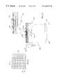
- FIG. 3 ashows one embodiment of an array of photodetectors, in simplified form.
- a rectangular matrix of only eight columns 50 and eight rows 52 of pixels 54is shown, to maintain clarity in the illustration.
- a matrix of at least 64 ⁇ 64 rows by columnswould be preferred, with larger matrices most preferred for better resolution.
- a suitable 64 ⁇ 64 arraycan be fabricated with dimensions of approximately 1.28 mm by 1.28 mm, for example.
- rectangular photodetector matricesare most common, other geometrical arrangements can be employed and are also within the scope of the invention.
- the photodetector at each pixelbe integrated with its own associated amplifier and integrator/latch circuit (taken together, the readout electronics 36 ).
- FIG. 4aA top detector layer 60 in which the photodetectors are fabricated is bonded via interconnects 62 (typically indium) to an amplifier layer 64 , which buffers and amplifies the photodetector signal.
- interconnects 62typically indium
- amplifier layer 64typically the photodetector 60 is fabricated in HgCdTe or InGaAs.
- the amplifier layer 64which is most suitably fabricated in CMOS (but could be fabricated in another technology such as GaAs or InGaAs or InP), optionally also includes, for each pixel, an integrator (with reset switches) and latch. The details of the amplifier layer circuitry are discussed below in connection with FIGS. 5 and 6.
- the detector layer 60is fabricated in the same materials as the amplifier circuits, preferably in either InGaAs or GaAs. This approach eliminates the need for extra semiconductor processing and substrate removal in the case where the amplifier is fabricated in the III-V technology rather than CMOS.
- the amplifier and detector layers(together layer 66 ) is then combined by wafer transfer with a CMOS layer 67 to which it is connected by interconnect layer 68 .
- the CMOS layer 67preferably includes an integrator, switch, and latch as well as multiplexing circuitry to read out the signals from all the pixels in a serial video stream.
- a suitable wafer transfer techniqueis described in U.S. Pat. No. 5,627,112.
- FIG. 5is an amplifier block diagram of an individual pixel's readout electronics 36 .
- Input signalis provided by an associated photodetector Pd (shown with associated intrinsic capacitance Cd).
- Pdshown with associated intrinsic capacitance Cd
- a two stage circuit configurationis shown, but fewer or more stages could be used.
- the input signalis amplified by an input charge (capacitive transimpedance) amplifier stage A 1 , which is configured essentially as an inverting integrator with capacitance Cl in the feedback path.
- the charge amplifiershould preferably provide very high charge sensitivity with very high speed, sufficient to measure delay of packet charge signal with a precision of approximately 1 nanosecond.
- a single ended cascode inverteris most suitable, using very high input impedance devices (an exemplary circuit is disclosed and discussed below, in connection with FIG. 6 ).
- the feedback capacitance C 1is typically the intrinsic capacitance of the devices, which is small (on the order of 5 femtofarads).
- the output of the first stage amplifieris preferably capacitively coupled (via capacitor C 2 on the order of 100 femtofarads) to a second stage inverting charge amplifier A 2 , shown with intrinsic capacitance C 3 in the feedback path.
- the second stageprovides additional gain.
- the output of the second stage amplifier A 2drives a latch L 1 , which is preferably fast regenerative comparators cross-connected in a latch configuration (one such circuit is shown below in FIG. 6 ).
- High speed semiconductor switches S 1 and S 2are provided to reset the first and second amplifier stages for initialization. These switches are closed to initialize the circuit by discharging any dark current or leakage charge buildup across capacitors C 1 and C 3 .
- An integrator 70(including amplifier A 3 and capacitor C 4 ), driven by a constant current source IS 1 , provides a means of timing the arrival of photons at the photodetector Pd. Initially, the integrator 70 is reset by a signal R 1 from timing electronics 44 . The reset signal closes the switches S 1 , S 2 S 4 , and R thereby discharging the capacitors C 1 , C 3 and C 4 and resetting the latch, L 1 . At a predetermined time (t( 0 )) with known temporal relationship to the laser pulse firing event, the switches are opened and the integrator 70 begins to integrate.
- the output of latch L 1goes high and opens a switch S 3 , thereby interrupting current from a constant current source IS 1 into an integrator circuit (the amplifier A 3 and feedback capacitor C 4 ).
- the voltage at OUTis thereby latched to a level proportional to the elapsed time from t( 0 ) to the time of arrival of the photons at Pd.
- the input charge amplifiers and high speed latch(collectively designated as the receiver amplifier 72 ) be extremely sensitive and extremely precise in time response.
- a sensitivity in the neighborhood of 5 ⁇ 10 15 Volts/Coulombis desirable, which is equivalent to approximately 0.8 millivolt/electron.
- An exemplary circuit which can fabricated in CMOS to provide these characteristicsis shown in FIG. 6 .
- FIG. 6the four transistors m 1 , m 2 , m 3 , and m 4 connected and biased as indicated constitute FIG. 5 amplifier Al; and the four transistors m 5 , m 6 , m 7 and m 8 connected and biased as indicated constitute FIG. 5 amplifier A 2 .
- the two NMOS transistors ml and m 2are connected in a cascode amplifier configuration which amplifies the signal from a photodetector Pd connected to input INN.
- the PMOS transistors m 3 and m 4provide a current source bias for the m 1 m 2 cascode circuit. Current bias is set by voltage references applied at VBUO, VBU, and VBO from a conventional voltage reference circuit (not shown) .
- a bias point providing quiescent current of approximately 10 microamps in the source/drain circuit of m 2is suitable.
- the reset switches S 1 and S 2 of FIG. 5are implemented as transistors msl and ms 2 in FIG. 6 . These NMOS transistors are operated in switching mode, with the switches closing on rising edge of the pulses at RES and VCO, respectively. These switches provide a means of initializing and resetting the charge amplifier (first and second stages) as discussed below.
- transistors m 5 and m 6(augmented by transistors m 7 and m 8 ) provide a second stage amplifier, also a cascode configuration, which further amplifies the output of the first stage “m1-m2” amplifier.
- Transistors m 7 and m 8provide the bias current to the m 5 -m 6 cascode amplifier, and are biased by a voltage reference circuit which sets the voltages VBUTO, VBU, and VBO as previously discussed in connection with the first amplifier stage.
- the output OUT 1 of the second stage amplifieris further amplified by the input stage (transistors m 9 and m 10 ) of the latch consisting of transistors m 9 , m 10 , m 11 , m 12 and m 13 with the latch reset (R in FIG. 5) being transistor m 3 .
- the latch resetR in FIG. 5
- the latchWhen the voltage at the drain of m 10 (OUT 2 ) is pulled low, it causes m 13 to conduct, pulling up voltage OUT 3 at the drain of m 13 . This condition turns off mll, thereby setting the m 11 -m 13 latch circuit into an “output-high” state.
- the latchremains set in the output-high state until reset by a low level at VC 1 , which causes mll to conduct, pulling up the voltage at OUT 2 and resetting the latch into the OUT 3 -low state.
- the three switchesshould preferably be opened in a specific sequence and timing, to reduce initial charge injection from the initialization.
- MS 1should open first, then MS 2 , then MS 3 .
- the gate voltages RES and VC 0which open MS 1 and MS 2 , respectively, should preferably be formed with approximately a 1 microsecond rise time.
- the waveform used for RESshould preferably lead the waveform used for VC 0 by about 20 ns.
- the timing diagram of FIG. 7shows a typical timing sequence generated by the invention.
- Reset pulses 80 (RES in FIG. 6) and 82 (Vc 0 in FIG. 6)are generated by the timing electronics ( 44 in FIG. 1) in the approximate relationship as shown, with 1 microsecond rise times and an approximate 20 ns lag between 80 and 82 , followed by a third reset 84 which resets MS 3 , also generated by the timing electronics 44 ).
- the laser pulsefires, indicated by pulse 86 .
- some transit time 88during which a light pulse travels from the laser, to an object, and returns to the photodetector, a charge pulse 90 is detected.
- the output OUT 3responds, latching quickly up to its supply voltage as shown. If desired in a particular application, the process can be repeated by resetting (by reset pulses identical to previous reset pulses 82 , 83 and 84 ). However, in many applications it is desirable to acquire image data using a single, non-repetitive pulse, or a short series of pulses. Such an approach is resistant to detection and location (countermeasures) from the subject, which may include hostile personnel or devices.
- the receiver amplifier 72have transient response rise times which are not sensitive to the amplitude of the input signal. In other words, to detect the distant of objects the device rise times should not depend on the reflectivity of the subject, which would otherwise introduce uncertainty into the measurement of elapsed time.
- the circuit shown in FIG. 6provides very low variation in rise time with different amplitude inputs, as demonstrated in FIG. 8, a simulation of transient response.
- FIG. 9shows a flow chart of a process preferably used under control of the processor 46 (in FIG. 2) to image objects by the invention.
- the light sourceis directed toward a subject of interest, typically by manual positioning (step 120 ).
- the detectoris oriented toward the subject (step 122 ).
- the processor 46triggers the timing circuits 44 to initialize the receiver pixels and trigger the light source (together step 124 ), preferably according to the timing sequence previously discussed in connection with FIG. 7 .
- the timing circuitsbegin timing (step 126 ).
- this timingis accomplished by a circuit such as the integrator 70 shown in FIG. 5 and discussed above.
- reflected light returns from the subjectis gathered and focused by an optical system, and is received (step 128 ) by the photodetector and receiver electronics.
- the output of the receiver electronicslatches the integrator (for each pixel, at various times, step 130 ) or otherwise stops the timing for each pixel.
- the processor 46determines for each pixel based on the integrator voltage the time of travel for the light detected at that pixel and calculates the corresponding distance to the target portion imaged at that pixel (step 132 ). Based upon the calculated distances, the processor 46 then develops an image including the distance information and displays that image on the display device 48 (shown in FIG. 2 ).
- a second pulse with a known different magnitudemay be used to increase the precision of the distance measurement. This is done by examining the difference in delay between pulses of different magnitude. Those pixels which show significant differences are those which have low response intensity. Knowing the response characteristics of the pixels will allow correction to extract more precise depth from the low response pixels.
- the photodetector Pd used in the inventionshould preferably be a semiconductor photodiode biased in its linear region, below the avalanche breakdown threshold.
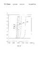
- One semiconductor photodetector structurewhich can be operated suitably in such a linear, non-geiger detection mode is shown in cross-section in FIG. 10, in connection with an energy level diagram of the corresponding layers.
- Each pixelpreferably includes a coextensive microlens 150 and transparent substrate layer 152 , which focus incident light 154 into an active region 156 of the pixel.
- the incident lightpasses through an (optional) buffer layer 158 , which is suitably fabricated on the order of 2 microns thick from a semiconductor material (preferably mercury telluride or similar material) which is transparent to the wavelengths of interest (typically around 1.5 micron wavelength).
- Photoelectrons produced in the depletion regionmigrate under the influence of the junction electric field to the p-implanted, diffused, or grown junction 162 and are picked up by a reflecting, conductive contact 164 to provide a signal.
- Other such structuresare possible, including avalanche photodiodes with sufficient uniformity in responsivity (gain times quantum efficiency) and low noise at the operating bias, provided that the structure used provides good quantum efficiency, typically >0.6 electron/photon.
- Pixel sizes of 20 ⁇ 20 micron areasare suitable. Overall photonic efficiency can be improved by the use of focusing microlenses to concentrate photonic energy in photodetector areas of the pixels, as is well known. Microlenses can also be used to allow larger pixel size without increasing detector capacitance or reducing sensitivity.
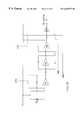
- FIG. 11An alternate embodiment of the invention features switchable modes, adding versatility.
- One exemplary circuit which can be used in the alternate embodimentis illustrated in FIG. 11 .
- the Latch L 1is bypassed by switch SBP which (when closed) couples the output of A 2 to the input of A 3 .
- Switch S 3should be open when operating in the alternate mode, disconnecting the current source IS 1 from the input of A 3 .
- the A 3 -C 4 integratorintegrates the signal from the input stages, accumulating the input over time.
- the switchable circuit shownperforms the same functions as described above, in connection with FIG. 5, but additionally is capable of operation in a passive or pulse integrating mode, by temporarily sacrificing the distance measurement. In a passive mode, the circuit of FIG.
- the usermight start surveillance of a subject area with passive mode, switching to full ranging and depth resolution mode when a target of greater interest is identified.
- At least two pulsesare used for improved depth resolution.
- the depth of the imaged sceneis small compared to its range from the apparatus of the invention.
- the problem of accurately measuring a small time difference in the context of a large total timeis solved by using a first pulse, which starts all pixel timers when it is received (at any pixel), and a second pulse with known temporal relation to the first pulse to stop each pixel's timer when light is received at that respective pixel. This provides a “vernier” to allow improved time resolution.
- the timing sequence used by the two-pulse or “vernier” embodimentis illustrated in FIG. 12 .
- the pulse sequence usedis a variant of the timing diagram of FIG. 7.
- a first light pulse 202is emitted, followed by a second light pulse 204 .
- the delay between pulses 202 and 204is preferably on the order of a few microseconds, which is long enough to allow the photo-receiver circuits to reset.
- the light pulsestravel from the source to the subject scene and back to the receiver during time T RT .
- the horizontal time scale of the FIG. 12has been intentionally distorted by greatly compressing the duration of T RT in order to fit the relevant events within the boundaries of the diagram).
- T RTAfter T RT the reflection of the first pulse 204 returns.
- An initial reflection 206(from a near surface of the subject scene) is closely followed by further reflections 208 from more distant surfaces.
- a timeris started upon receipt 206 of the reflection from the closest surface of the subject scene (the first reflection received, at whatever pixel that occurs).
- the timingis performed by integrating a constant current in the same manner shown in FIG. 5 .
- the integratorsare started in each pixel upon the receipt of pulse 206 , the reset switches S 1 and S 2 are not opened until an appropriate delay has occurred to allow later returns from the initial pulse to die away. This may be accomplished with the existing above described circuit by emitting pulses on successive frames, with the return from the first frame being used to time the opening of the reset switch on the second frame. In this mode the current from the calibrated source is set much higher in the second frame to provide the vernier.
- Waveform 214shows the output voltage at a nearest pixel P 1 .
- the output voltagestarts from zero, and begins to ramp upward as the integrator accumulates charge, beginning from time 218 which is T reset after the reception of reflection 206 .
- Pixel P 1receives an optical signal from pulse return 210 , which latches the integrator at an output voltage VP 1 by opening a switch (as in FIG. 5 ).
- Another pixel, arbitrarily denoted P 2receives an optical return 212 later, because it receives light imaged from a more distant surface of the scene.
- the voltage 216 at the integrator for P 2integrates for a longer time, reaching the voltage VP 2 (higher than VP 1 ).
- the processor 46(in FIG. 2) then assembles an image based on the various voltages reached by the various pixels, as in the previously described embodiments.
- One advantage of the “vernier” embodimentis the increased accuracy obtained because the integration takes place for a shorter period as compared with timing a pulse from emission to reception, allowing the use of higher currents in the integrators.
- a clockoutputs a measured disabling pulse, such as is shown at 226 .
- the integrators at all pixelsare disabled until clock pulse 226 falls, allowing a user to set an effective minimum or “front” range for the imaging device. Scenes in front of the preset minimum range will not contribute to the image.
- two pulsesare used to provide a useful “look-behind” ability.
- a subject scenehas multiple “layers” of partially reflecting surface.
- a large metallic objectmay be concealed behind a thin layer of netting or foliage, or a subject of interest might be partially or completely hidden under water or behind a partially transparent surface.
- the signal return even at a single pixelmight have multiple peaks, one from the nearer surface and another (at least one) from the more distant surfaces (the “behind surfaces”).
- an adjustable blanking timeis used to disable all the pixels' receivers for a predetermined time (which may be based on the return from a previous frame), to allow the return from the nearer surface to pass by the temporarily disabled receiver.
- a suitable timing sequenceis shown which can be controlled by programming processor 46 to command the indicated timing sequences from timing circuits 44 .
- Optical pulse 202is emitted first, followed shortly thereafter by second optical pulse 204 , as in the previous figures.
- the optical return 230which indicates the return from a single representative pixel P 3 , shows multiple peaks from each optical pulse emitted.
- a first peak 232corresponds to the reflection from a near, concealing surface of the subject scene;
- a second peak 238corresponds to a second, deeper reflection from a farther surface of the same scene, received by the same pixel because the two surfaces are directly in line with the optical line of sight.
- second pulse 204produces two returns 240 and 242 , respectively from a nearer and a farther surface of the subject scene.
- a blanking pulse 244is provided which keeps pixel 3 in the reset mode (S 1 , S 2 , and R switches all closed) until time 246 when the reset switches are opened rapidly in the above mentioned sequence ( 82 - 83 - 84 in FIG. 7 ).
- the blanking period set by pulse 244can suitably be set slightly greater than the shortest measured round trip time at any pixel of the reflection from the first pulse 202 , which establishes a near extreme for the object range.
- the blanking period of pulse 244is sufficiently long that the receiver is still disabled when pulse 240 arrives, so this pulse is ignored.
- Waveform 250represents the integrator voltage at a a pixel disposed to receive return 242 .
- T blankBy adjusting the length of blanking period T blank , the near boundary can be adjusted closer or farther from the apparatus.
- the inventionallows a user to look behind the nearest surfaces, which may disguise a subject scene of greater interest. For example, a large vehicle parked behind partial foliage or getting could be imaged by setting the boundary beyond the screening foliage or netting. The limit of the distance resolvable behind the obscuration is determined by the time required to reset the pixel after the reset switches are opened.
- the inventionrepeats the timing sequence of FIG. 13 in (at least one) successive time frames, incrementing in each successive frame the length of T BLANK .
- Each frame's returnis used to construct an image corresponding to object projections on successively more distant surfaces, corresponding to the successively increasing T BLANK .
- An ensemble of image framesresults, which is used to construct a three-dimensional image of the object, including obscured features revealed by the “look-behind” capability.
- FIG. 14shows a circuit variation which is very similar to the charge amplifiers of FIG. 5 but which includes an additional amplifier stage A 4 between A 2 and the latch L 1 .
- the circuitis enabled by opening CR 0 , CR 1 and CR 2 , preferably in that order. This circuit provides faster transition from the disabled to the enabled state, and would be suitable in an application in which such fast enable time is highly desirable.
Landscapes
- Engineering & Computer Science (AREA)
- Physics & Mathematics (AREA)
- Computer Networks & Wireless Communication (AREA)
- General Physics & Mathematics (AREA)
- Radar, Positioning & Navigation (AREA)
- Remote Sensing (AREA)
- Electromagnetism (AREA)
- Optical Radar Systems And Details Thereof (AREA)
Abstract
Description
| TABLE 2 | |||
| Charge e- | Relative switching time | ||
| 337 -> 487 | 2 ns | ||
| 487 -> 637 | 1.3 ns | ||
| 637 -> 787 | 0.75 ns | ||
| 787 -> 937 | 0.5 ns | ||
Claims (3)
Priority Applications (1)
| Application Number | Priority Date | Filing Date | Title |
|---|---|---|---|
| US09/408,329US6448572B1 (en) | 1999-09-29 | 1999-09-29 | Ranging three-dimensional laser imager and method |
Applications Claiming Priority (1)
| Application Number | Priority Date | Filing Date | Title |
|---|---|---|---|
| US09/408,329US6448572B1 (en) | 1999-09-29 | 1999-09-29 | Ranging three-dimensional laser imager and method |
Publications (1)
| Publication Number | Publication Date |
|---|---|
| US6448572B1true US6448572B1 (en) | 2002-09-10 |
Family
ID=23615816
Family Applications (1)
| Application Number | Title | Priority Date | Filing Date |
|---|---|---|---|
| US09/408,329Expired - LifetimeUS6448572B1 (en) | 1999-09-29 | 1999-09-29 | Ranging three-dimensional laser imager and method |
Country Status (1)
| Country | Link |
|---|---|
| US (1) | US6448572B1 (en) |
Cited By (46)
| Publication number | Priority date | Publication date | Assignee | Title |
|---|---|---|---|---|
| US20020060784A1 (en)* | 2000-07-19 | 2002-05-23 | Utah State University | 3D multispectral lidar |
| US6661500B1 (en)* | 2002-03-15 | 2003-12-09 | National Semiconductor Corporation | Integrated range finder and imager |
| US20030234347A1 (en)* | 2002-03-13 | 2003-12-25 | Omron Corporation | Monitor |
| US6678039B2 (en)* | 2001-05-23 | 2004-01-13 | Canesta, Inc. | Method and system to enhance dynamic range conversion useable with CMOS three-dimensional imaging |
| FR2848368A1 (en)* | 2002-12-06 | 2004-06-11 | Thales Sa | THREE-DIMENSIONAL ACTIVE IMAGING SYSTEM OF AN OBJECT |
| US20040169842A1 (en)* | 2002-03-27 | 2004-09-02 | Sarnoff Corporation | Method and apparatus for generating charge from a light pulse |
| US20050051707A1 (en)* | 2003-04-11 | 2005-03-10 | Cyrus Bamji | Method and system to differentially enhance sensor dynamic range |
| US20060006309A1 (en)* | 2004-07-06 | 2006-01-12 | Jerry Dimsdale | Method and apparatus for high resolution 3D imaging |
| US20060007422A1 (en)* | 2004-07-06 | 2006-01-12 | Jerry Dimsdale | System and method for determining range in 3D imaging systems |
| US20060027730A1 (en)* | 2003-04-11 | 2006-02-09 | Cyrus Bamji | Method and system to differentially enhance sensor dynamic range using enhanced common mode reset |
| US20070206952A1 (en)* | 2005-08-04 | 2007-09-06 | Kazutoshi Hase | Optical transmitter |
| US7342228B1 (en)* | 2002-09-06 | 2008-03-11 | Oceanit Laboratories, Inc. | Method and apparatus for measurement of aerosols and imaging |
| US20080166970A1 (en)* | 2007-01-09 | 2008-07-10 | Innovative Sonic Limited | Method and apparatus for handling reset in a wireless communications system |
| US7486854B2 (en) | 2006-01-24 | 2009-02-03 | Uni-Pixel Displays, Inc. | Optical microstructures for light extraction and control |
| US7649202B2 (en) | 2004-06-25 | 2010-01-19 | Samsung Mobile Display Co., Ltd. | Transistor, method of fabricating the same, and light emitting display comprising the same |
| US20100102203A1 (en)* | 2008-01-17 | 2010-04-29 | Ball Aerospace & Technologies Corp. | Pulse data recorder |
| US20100208244A1 (en)* | 2008-05-09 | 2010-08-19 | Ball Aerospace & Technologies Corp. | Flash ladar system |
| US7894044B1 (en) | 2008-03-11 | 2011-02-22 | Oceanit Laboratories, Inc. | Laser for coherent LIDAR |
| US7929215B1 (en) | 2009-02-20 | 2011-04-19 | Ball Aerospace & Technologies Corp. | Field widening lens |
| US7995191B1 (en)* | 2006-06-29 | 2011-08-09 | Sandia Corporation | Scannerless laser range imaging using loss modulation |
| US8077294B1 (en) | 2008-01-17 | 2011-12-13 | Ball Aerospace & Technologies Corp. | Optical autocovariance lidar |
| US20120274947A1 (en)* | 2009-12-23 | 2012-11-01 | Thales | Device for Detecting Laser Spot with Matrix Deviometer |
| US8306273B1 (en) | 2009-12-28 | 2012-11-06 | Ball Aerospace & Technologies Corp. | Method and apparatus for LIDAR target identification and pose estimation |
| US20130114065A1 (en)* | 2011-11-09 | 2013-05-09 | Cheng Uei Precision Industry Co., Ltd. | Method for measuring the heights of components based on laser ranging |
| US8736818B2 (en) | 2010-08-16 | 2014-05-27 | Ball Aerospace & Technologies Corp. | Electronically steered flash LIDAR |
| US8744126B1 (en) | 2012-03-07 | 2014-06-03 | Ball Aerospace & Technologies Corp. | Morphology based hazard detection |
| DE112004000035B4 (en)* | 2003-07-09 | 2015-03-19 | Conti Temic Microelectronic Gmbh | Sensor arrangement for distance and / or speed measurement |
| US9041915B2 (en) | 2008-05-09 | 2015-05-26 | Ball Aerospace & Technologies Corp. | Systems and methods of scene and action capture using imaging system incorporating 3D LIDAR |
| US20150338509A1 (en)* | 2012-12-17 | 2015-11-26 | Pmdtechnologies Gmbh | Time-of-flight camera with motion detection |
| US9360554B2 (en) | 2014-04-11 | 2016-06-07 | Facet Technology Corp. | Methods and apparatus for object detection and identification in a multiple detector lidar array |
| BE1023688B1 (en)* | 2015-03-30 | 2017-06-15 | Hamilton Sundstrand Corporation | PIXEL FOR PULSE DETECTION AND DIGITAL IMAGING |
| US9866816B2 (en) | 2016-03-03 | 2018-01-09 | 4D Intellectual Properties, Llc | Methods and apparatus for an active pulsed 4D camera for image acquisition and analysis |
| EP3167304A4 (en)* | 2014-07-08 | 2018-02-21 | Basf Se | Detector for determining a position of at least one object |
| US10036801B2 (en) | 2015-03-05 | 2018-07-31 | Big Sky Financial Corporation | Methods and apparatus for increased precision and improved range in a multiple detector LiDAR array |
| US10203399B2 (en) | 2013-11-12 | 2019-02-12 | Big Sky Financial Corporation | Methods and apparatus for array based LiDAR systems with reduced interference |
| US20190195991A1 (en)* | 2017-12-22 | 2019-06-27 | Denso Corporation | Distance measuring apparatus, recognizing apparatus, and distance measuring method |
| US20190266741A1 (en)* | 2018-02-23 | 2019-08-29 | Toyota Motor Engineering & Manufacturing North America, Inc. | System and method for object detection using edge characteristics |
| US10458904B2 (en) | 2015-09-28 | 2019-10-29 | Ball Aerospace & Technologies Corp. | Differential absorption lidar |
| US10823825B2 (en) | 2016-05-02 | 2020-11-03 | 3Deo, Inc | System and method for wide-area surveillance |
| US10921245B2 (en) | 2018-06-08 | 2021-02-16 | Ball Aerospace & Technologies Corp. | Method and systems for remote emission detection and rate determination |
| CN113126105A (en)* | 2019-12-30 | 2021-07-16 | 睿镞科技(北京)有限责任公司 | Three-dimensional distance measurement method and device |
| WO2023066052A1 (en)* | 2021-10-21 | 2023-04-27 | 华为技术有限公司 | Detection method and apparatus |
| US11933967B2 (en) | 2019-08-22 | 2024-03-19 | Red Creamery, LLC | Distally actuated scanning mirror |
| US12123950B2 (en) | 2016-02-15 | 2024-10-22 | Red Creamery, LLC | Hybrid LADAR with co-planar scanning and imaging field-of-view |
| US12399278B1 (en) | 2016-02-15 | 2025-08-26 | Red Creamery Llc | Hybrid LIDAR with optically enhanced scanned laser |
| US12399279B1 (en) | 2016-02-15 | 2025-08-26 | Red Creamery Llc | Enhanced hybrid LIDAR with high-speed scanning |
Citations (5)
| Publication number | Priority date | Publication date | Assignee | Title |
|---|---|---|---|---|
| US4727259A (en)* | 1986-02-24 | 1988-02-23 | The United States Of America As Represented By The Secretary Of The Air Force | Monolithic area array with shutter operable to only transmit light between the minimum and maximum ranges for laser rangefinding |
| US4794262A (en)* | 1985-12-03 | 1988-12-27 | Yukio Sato | Method and apparatus for measuring profile of three-dimensional object |
| US5835204A (en)* | 1995-12-18 | 1998-11-10 | State Of Israel/Ministry Of Defense | Laser ranging system |
| US5892575A (en) | 1996-05-10 | 1999-04-06 | Massachusetts Institute Of Technology | Method and apparatus for imaging a scene using a light detector operating in non-linear geiger-mode |
| US6323942B1 (en)* | 1999-04-30 | 2001-11-27 | Canesta, Inc. | CMOS-compatible three-dimensional image sensor IC |
- 1999
- 1999-09-29USUS09/408,329patent/US6448572B1/ennot_activeExpired - Lifetime
Patent Citations (5)
| Publication number | Priority date | Publication date | Assignee | Title |
|---|---|---|---|---|
| US4794262A (en)* | 1985-12-03 | 1988-12-27 | Yukio Sato | Method and apparatus for measuring profile of three-dimensional object |
| US4727259A (en)* | 1986-02-24 | 1988-02-23 | The United States Of America As Represented By The Secretary Of The Air Force | Monolithic area array with shutter operable to only transmit light between the minimum and maximum ranges for laser rangefinding |
| US5835204A (en)* | 1995-12-18 | 1998-11-10 | State Of Israel/Ministry Of Defense | Laser ranging system |
| US5892575A (en) | 1996-05-10 | 1999-04-06 | Massachusetts Institute Of Technology | Method and apparatus for imaging a scene using a light detector operating in non-linear geiger-mode |
| US6323942B1 (en)* | 1999-04-30 | 2001-11-27 | Canesta, Inc. | CMOS-compatible three-dimensional image sensor IC |
Cited By (92)
| Publication number | Priority date | Publication date | Assignee | Title |
|---|---|---|---|---|
| US20020060784A1 (en)* | 2000-07-19 | 2002-05-23 | Utah State University | 3D multispectral lidar |
| US6664529B2 (en)* | 2000-07-19 | 2003-12-16 | Utah State University | 3D multispectral lidar |
| US6678039B2 (en)* | 2001-05-23 | 2004-01-13 | Canesta, Inc. | Method and system to enhance dynamic range conversion useable with CMOS three-dimensional imaging |
| US20030234347A1 (en)* | 2002-03-13 | 2003-12-25 | Omron Corporation | Monitor |
| US7164116B2 (en)* | 2002-03-13 | 2007-01-16 | Omron Corporation | Monitor for intrusion detection |
| US6661500B1 (en)* | 2002-03-15 | 2003-12-09 | National Semiconductor Corporation | Integrated range finder and imager |
| US20040169842A1 (en)* | 2002-03-27 | 2004-09-02 | Sarnoff Corporation | Method and apparatus for generating charge from a light pulse |
| US6924887B2 (en)* | 2002-03-27 | 2005-08-02 | Sarnoff Corporation | Method and apparatus for generating charge from a light pulse |
| US7342228B1 (en)* | 2002-09-06 | 2008-03-11 | Oceanit Laboratories, Inc. | Method and apparatus for measurement of aerosols and imaging |
| FR2848368A1 (en)* | 2002-12-06 | 2004-06-11 | Thales Sa | THREE-DIMENSIONAL ACTIVE IMAGING SYSTEM OF AN OBJECT |
| WO2004112090A3 (en)* | 2002-12-17 | 2005-03-10 | Sarnoff Corp | Method and apparatus for generating charge from a light pulse |
| US20050051707A1 (en)* | 2003-04-11 | 2005-03-10 | Cyrus Bamji | Method and system to differentially enhance sensor dynamic range |
| US20060027730A1 (en)* | 2003-04-11 | 2006-02-09 | Cyrus Bamji | Method and system to differentially enhance sensor dynamic range using enhanced common mode reset |
| US6919549B2 (en) | 2003-04-11 | 2005-07-19 | Canesta, Inc. | Method and system to differentially enhance sensor dynamic range |
| US7176438B2 (en) | 2003-04-11 | 2007-02-13 | Canesta, Inc. | Method and system to differentially enhance sensor dynamic range using enhanced common mode reset |
| DE112004000035B4 (en)* | 2003-07-09 | 2015-03-19 | Conti Temic Microelectronic Gmbh | Sensor arrangement for distance and / or speed measurement |
| US7649202B2 (en) | 2004-06-25 | 2010-01-19 | Samsung Mobile Display Co., Ltd. | Transistor, method of fabricating the same, and light emitting display comprising the same |
| US20090076758A1 (en)* | 2004-07-06 | 2009-03-19 | Dimsdale Engineering, Llc. | System and method for determining range in 3d imaging systems |
| US20100188504A1 (en)* | 2004-07-06 | 2010-07-29 | Dimsdale Engineering, Llc | Method and apparatus for high resolution 3d imaging as a function of camera position, camera trajectory and range |
| US20070252974A1 (en)* | 2004-07-06 | 2007-11-01 | Dimsdale Engineering, Llc. | System and method for determining range in 3d imaging systems |
| US7236235B2 (en) | 2004-07-06 | 2007-06-26 | Dimsdale Engineering, Llc | System and method for determining range in 3D imaging systems |
| US8547532B2 (en) | 2004-07-06 | 2013-10-01 | Topcon Positioning Systems, Inc. | System and method for determining range in 3D imaging systems |
| US7453553B2 (en) | 2004-07-06 | 2008-11-18 | Dimsdale Engineering, Llc | System and method for determining range in 3D imaging systems |
| US20060006309A1 (en)* | 2004-07-06 | 2006-01-12 | Jerry Dimsdale | Method and apparatus for high resolution 3D imaging |
| WO2006014445A1 (en)* | 2004-07-06 | 2006-02-09 | Dimsdale Engineering, Llc | Method and apparatus for high resolution 3d imaging |
| US20060007422A1 (en)* | 2004-07-06 | 2006-01-12 | Jerry Dimsdale | System and method for determining range in 3D imaging systems |
| US7991222B2 (en) | 2004-07-06 | 2011-08-02 | Topcon Positioning Systems, Inc. | Method and apparatus for high resolution 3D imaging as a function of camera position, camera trajectory and range |
| US7697748B2 (en) | 2004-07-06 | 2010-04-13 | Dimsdale Engineering, Llc | Method and apparatus for high resolution 3D imaging as a function of camera position, camera trajectory and range |
| US7657182B2 (en)* | 2005-08-04 | 2010-02-02 | Panasonic Corporation | Liquid lens optical transmitter system |
| US20070206952A1 (en)* | 2005-08-04 | 2007-09-06 | Kazutoshi Hase | Optical transmitter |
| US8218920B2 (en) | 2006-01-24 | 2012-07-10 | Rambus Inc. | Optical microstructures for light extraction and control |
| US7486854B2 (en) | 2006-01-24 | 2009-02-03 | Uni-Pixel Displays, Inc. | Optical microstructures for light extraction and control |
| US8380026B2 (en) | 2006-01-24 | 2013-02-19 | Rambus Inc. | Optical microstructures for light extraction and control |
| US7995191B1 (en)* | 2006-06-29 | 2011-08-09 | Sandia Corporation | Scannerless laser range imaging using loss modulation |
| US20080166970A1 (en)* | 2007-01-09 | 2008-07-10 | Innovative Sonic Limited | Method and apparatus for handling reset in a wireless communications system |
| US8081648B2 (en)* | 2007-01-09 | 2011-12-20 | Innovative Sonic Limited | Method and apparatus for handling reset in a wireless communications system |
| US8232514B2 (en) | 2008-01-17 | 2012-07-31 | Ball Aerospace & Technologies Corp. | Method using a switch and memory to count events |
| US8077294B1 (en) | 2008-01-17 | 2011-12-13 | Ball Aerospace & Technologies Corp. | Optical autocovariance lidar |
| US20100102203A1 (en)* | 2008-01-17 | 2010-04-29 | Ball Aerospace & Technologies Corp. | Pulse data recorder |
| US8119971B2 (en) | 2008-01-17 | 2012-02-21 | Ball Corporation | Pulse data recorder in which a value held by a bit of a memory is determined by a state of a switch |
| US7894044B1 (en) | 2008-03-11 | 2011-02-22 | Oceanit Laboratories, Inc. | Laser for coherent LIDAR |
| US20100208244A1 (en)* | 2008-05-09 | 2010-08-19 | Ball Aerospace & Technologies Corp. | Flash ladar system |
| US7961301B2 (en) | 2008-05-09 | 2011-06-14 | Ball Aerospace & Technologies Corp. | Flash LADAR system |
| US9041915B2 (en) | 2008-05-09 | 2015-05-26 | Ball Aerospace & Technologies Corp. | Systems and methods of scene and action capture using imaging system incorporating 3D LIDAR |
| US8314992B1 (en) | 2009-02-20 | 2012-11-20 | Ball Aerospace & Technologies Corp. | Field widening lens |
| US7929215B1 (en) | 2009-02-20 | 2011-04-19 | Ball Aerospace & Technologies Corp. | Field widening lens |
| US20120274947A1 (en)* | 2009-12-23 | 2012-11-01 | Thales | Device for Detecting Laser Spot with Matrix Deviometer |
| US9964622B2 (en)* | 2009-12-23 | 2018-05-08 | Thales | Device for detecting laser spot with matrix deviometer having a readout circuit and a matrix of photodiodes |
| US8306273B1 (en) | 2009-12-28 | 2012-11-06 | Ball Aerospace & Technologies Corp. | Method and apparatus for LIDAR target identification and pose estimation |
| US8736818B2 (en) | 2010-08-16 | 2014-05-27 | Ball Aerospace & Technologies Corp. | Electronically steered flash LIDAR |
| US20130114065A1 (en)* | 2011-11-09 | 2013-05-09 | Cheng Uei Precision Industry Co., Ltd. | Method for measuring the heights of components based on laser ranging |
| US8508719B2 (en)* | 2011-11-09 | 2013-08-13 | Cheng Uei Precision Industry Co., Ltd. | Method for measuring the heights of components based on laser ranging |
| US8744126B1 (en) | 2012-03-07 | 2014-06-03 | Ball Aerospace & Technologies Corp. | Morphology based hazard detection |
| US20150338509A1 (en)* | 2012-12-17 | 2015-11-26 | Pmdtechnologies Gmbh | Time-of-flight camera with motion detection |
| US9625569B2 (en)* | 2012-12-17 | 2017-04-18 | pmdtechnologies ag | Time-of-flight camera with motion detection |
| US10203399B2 (en) | 2013-11-12 | 2019-02-12 | Big Sky Financial Corporation | Methods and apparatus for array based LiDAR systems with reduced interference |
| US12313782B2 (en) | 2013-11-12 | 2025-05-27 | Sos Lab Co., Ltd. | Methods and apparatus for array based LiDAR systems with reduced interference |
| US12298438B2 (en) | 2013-11-12 | 2025-05-13 | Sos Lab Co., Ltd. | Methods and apparatus for array based LiDAR systems with reduced interference |
| US12078756B2 (en) | 2013-11-12 | 2024-09-03 | Sos Lab Co., Ltd. | Methods and apparatus for array based lidar systems with reduced interference |
| US11131755B2 (en) | 2013-11-12 | 2021-09-28 | Big Sky Financial Corporation | Methods and apparatus for array based LiDAR systems with reduced interference |
| US11860314B2 (en) | 2014-04-11 | 2024-01-02 | Big Sky Financial Corporation | Methods and apparatus for object detection and identification in a multiple detector lidar array |
| US9360554B2 (en) | 2014-04-11 | 2016-06-07 | Facet Technology Corp. | Methods and apparatus for object detection and identification in a multiple detector lidar array |
| US10585175B2 (en) | 2014-04-11 | 2020-03-10 | Big Sky Financial Corporation | Methods and apparatus for object detection and identification in a multiple detector lidar array |
| US11041718B2 (en)* | 2014-07-08 | 2021-06-22 | Basf Se | Detector for determining a position of at least one object |
| EP3167304A4 (en)* | 2014-07-08 | 2018-02-21 | Basf Se | Detector for determining a position of at least one object |
| US10036801B2 (en) | 2015-03-05 | 2018-07-31 | Big Sky Financial Corporation | Methods and apparatus for increased precision and improved range in a multiple detector LiDAR array |
| US11226398B2 (en) | 2015-03-05 | 2022-01-18 | Big Sky Financial Corporation | Methods and apparatus for increased precision and improved range in a multiple detector LiDAR array |
| BE1023688B1 (en)* | 2015-03-30 | 2017-06-15 | Hamilton Sundstrand Corporation | PIXEL FOR PULSE DETECTION AND DIGITAL IMAGING |
| US9698182B2 (en) | 2015-03-30 | 2017-07-04 | Hamilton Sundstrand Corporation | Digital imaging and pulse detection array |
| US10458904B2 (en) | 2015-09-28 | 2019-10-29 | Ball Aerospace & Technologies Corp. | Differential absorption lidar |
| US12399279B1 (en) | 2016-02-15 | 2025-08-26 | Red Creamery Llc | Enhanced hybrid LIDAR with high-speed scanning |
| US12399278B1 (en) | 2016-02-15 | 2025-08-26 | Red Creamery Llc | Hybrid LIDAR with optically enhanced scanned laser |
| US12123950B2 (en) | 2016-02-15 | 2024-10-22 | Red Creamery, LLC | Hybrid LADAR with co-planar scanning and imaging field-of-view |
| US10623716B2 (en) | 2016-03-03 | 2020-04-14 | 4D Intellectual Properties, Llc | Object identification and material assessment using optical profiles |
| US11838626B2 (en) | 2016-03-03 | 2023-12-05 | 4D Intellectual Properties, Llc | Methods and apparatus for an active pulsed 4D camera for image acquisition and analysis |
| US12096121B2 (en) | 2016-03-03 | 2024-09-17 | 4D Intellectual Properties, Llc | Precision reflectivity and ambient light removal for a geiger mode/single photon active sensor system |
| US10873738B2 (en) | 2016-03-03 | 2020-12-22 | 4D Intellectual Properties, Llc | Multi-frame range gating for lighting-invariant depth maps for in-motion applications and attenuating environments |
| US11477363B2 (en) | 2016-03-03 | 2022-10-18 | 4D Intellectual Properties, Llc | Intelligent control module for utilizing exterior lighting in an active imaging system |
| US12418719B2 (en) | 2016-03-03 | 2025-09-16 | 4D Intellectual Properties, Llc | Vehicle headlamp lighting control module for adas and autonomous vehicles |
| US10298908B2 (en) | 2016-03-03 | 2019-05-21 | 4D Intellectual Properties, Llc | Vehicle display system for low visibility objects and adverse environmental conditions |
| US10382742B2 (en) | 2016-03-03 | 2019-08-13 | 4D Intellectual Properties, Llc | Methods and apparatus for a lighting-invariant image sensor for automated object detection and vision systems |
| US9866816B2 (en) | 2016-03-03 | 2018-01-09 | 4D Intellectual Properties, Llc | Methods and apparatus for an active pulsed 4D camera for image acquisition and analysis |
| US10823825B2 (en) | 2016-05-02 | 2020-11-03 | 3Deo, Inc | System and method for wide-area surveillance |
| US11662433B2 (en)* | 2017-12-22 | 2023-05-30 | Denso Corporation | Distance measuring apparatus, recognizing apparatus, and distance measuring method |
| US20190195991A1 (en)* | 2017-12-22 | 2019-06-27 | Denso Corporation | Distance measuring apparatus, recognizing apparatus, and distance measuring method |
| US10664974B2 (en)* | 2018-02-23 | 2020-05-26 | Toyota Motor Engineering & Manufacturing North America, Inc. | System and method for object detection using edge characteristics |
| US20190266741A1 (en)* | 2018-02-23 | 2019-08-29 | Toyota Motor Engineering & Manufacturing North America, Inc. | System and method for object detection using edge characteristics |
| US10921245B2 (en) | 2018-06-08 | 2021-02-16 | Ball Aerospace & Technologies Corp. | Method and systems for remote emission detection and rate determination |
| US12130426B2 (en) | 2019-08-22 | 2024-10-29 | Red Creamery Llc | Distally actuated scanning mirror |
| US11933967B2 (en) | 2019-08-22 | 2024-03-19 | Red Creamery, LLC | Distally actuated scanning mirror |
| CN113126105A (en)* | 2019-12-30 | 2021-07-16 | 睿镞科技(北京)有限责任公司 | Three-dimensional distance measurement method and device |
| WO2023066052A1 (en)* | 2021-10-21 | 2023-04-27 | 华为技术有限公司 | Detection method and apparatus |
Similar Documents
| Publication | Publication Date | Title |
|---|---|---|
| US6448572B1 (en) | Ranging three-dimensional laser imager and method | |
| Seo et al. | Direct TOF scanning LiDAR sensor with two-step multievent histogramming TDC and embedded interference filter | |
| US6414746B1 (en) | 3-D imaging multiple target laser radar | |
| US6323941B1 (en) | Sensor assembly for imaging passive infrared and active LADAR and method for same | |
| KR101942103B1 (en) | A detector pixel signal readout circuit | |
| US6535275B2 (en) | High resolution 3-D imaging range finder | |
| KR102734518B1 (en) | Methods and systems for high-resolution, long-range flash LIDAR | |
| US6133989A (en) | 3D imaging laser radar | |
| Williams Jr | Optimization of eyesafe avalanche photodiode lidar for automobile safety and autonomous navigation systems | |
| US10401147B2 (en) | Dimensioning system | |
| US4757200A (en) | Pulsed radiation detection system | |
| IL258130A (en) | Time of flight distance sensor | |
| US20040169842A1 (en) | Method and apparatus for generating charge from a light pulse | |
| GB2421383A (en) | Surface profile measurement | |
| Aull et al. | Three-dimensional imaging with arrays of Geiger-mode avalanche photodiodes | |
| CN111103057B (en) | Photonic sensing with threshold detection using capacitor-based comparators | |
| US8421016B2 (en) | Laser-pulse matrix detector with rapid summation | |
| US5354981A (en) | Switching photosensitive matrix device | |
| Browder et al. | Three-dimensional imaging sensors program | |
| US10154207B2 (en) | Event-triggered imaging pixels | |
| Huntington et al. | 512-element linear InGaAs APD array sensor for scanned time-of-flight lidar at 1550 nm | |
| Johnson et al. | Adaptive LaDAR receiver for multispectral imaging | |
| JP2021025810A (en) | Distance image sensor, and distance image measurement device | |
| US20250130318A1 (en) | Lidar system having optical back scatter recovery | |
| Martin et al. | A 640× 512 InGaAs camera for range-gated and staring applications |
Legal Events
| Date | Code | Title | Description |
|---|---|---|---|
| AS | Assignment | Owner name:ROCKWELL SCIENCE CENTER, LL, CALIFORNIA Free format text:ASSIGNMENT OF ASSIGNORS INTEREST;ASSIGNORS:TENNANT, WILLIAM E.;TOMASINI, ALFREDO;REEL/FRAME:010284/0247 Effective date:19990929 | |
| STCF | Information on status: patent grant | Free format text:PATENTED CASE | |
| FPAY | Fee payment | Year of fee payment:4 | |
| AS | Assignment | Owner name:ROCKWELL TECHNOLOGIES, LLC, CALIFORNIA Free format text:ASSIGNMENT OF ASSIGNORS INTEREST;ASSIGNOR:ROCKWELL SCIENCE CENTER, LLC;REEL/FRAME:018160/0122 Effective date:20000330 Owner name:INNOVATIVE TECHNOLOGY LICENSING, LLC, CALIFORNIA Free format text:CHANGE OF NAME;ASSIGNOR:ROCKWELL TECHNOLOGIES, LLC;REEL/FRAME:018160/0240 Effective date:20010628 Owner name:ROCKWELL SCIENTIFIC LICENSING, LLC, CALIFORNIA Free format text:CHANGE OF NAME;ASSIGNOR:INNOVATIVE TECHNOLOGY LICENSING, LLC;REEL/FRAME:018160/0250 Effective date:20030919 | |
| AS | Assignment | Owner name:TELEDYNE LICENSING, LLC, CALIFORNIA Free format text:CHANGE OF NAME;ASSIGNOR:ROCKWELL SCIENTIFIC LICENSING, LLC;REEL/FRAME:018573/0649 Effective date:20060918 | |
| FPAY | Fee payment | Year of fee payment:8 | |
| AS | Assignment | Owner name:TELEDYNE SCIENTIFIC & IMAGING, LLC, CALIFORNIA Free format text:MERGER;ASSIGNOR:TELEDYNE LICENSING, LLC;REEL/FRAME:027830/0206 Effective date:20111221 | |
| FEPP | Fee payment procedure | Free format text:PAYOR NUMBER ASSIGNED (ORIGINAL EVENT CODE: ASPN); ENTITY STATUS OF PATENT OWNER: LARGE ENTITY | |
| FPAY | Fee payment | Year of fee payment:12 |