US6448160B1 - Method of fabricating power rectifier device to vary operating parameters and resulting device - Google Patents
Method of fabricating power rectifier device to vary operating parameters and resulting deviceDownload PDFInfo
- Publication number
- US6448160B1 US6448160B1US09/544,730US54473000AUS6448160B1US 6448160 B1US6448160 B1US 6448160B1US 54473000 AUS54473000 AUS 54473000AUS 6448160 B1US6448160 B1US 6448160B1
- Authority
- US
- United States
- Prior art keywords
- dopant
- conductivity type
- forming
- gate
- major surface
- Prior art date
- Legal status (The legal status is an assumption and is not a legal conclusion. Google has not performed a legal analysis and makes no representation as to the accuracy of the status listed.)
- Expired - Lifetime
Links
Images


Classifications
- H—ELECTRICITY
- H10—SEMICONDUCTOR DEVICES; ELECTRIC SOLID-STATE DEVICES NOT OTHERWISE PROVIDED FOR
- H10D—INORGANIC ELECTRIC SEMICONDUCTOR DEVICES
- H10D30/00—Field-effect transistors [FET]
- H10D30/60—Insulated-gate field-effect transistors [IGFET]
- H10D30/64—Double-diffused metal-oxide semiconductor [DMOS] FETs
- H10D30/66—Vertical DMOS [VDMOS] FETs
- H—ELECTRICITY
- H01—ELECTRIC ELEMENTS
- H01L—SEMICONDUCTOR DEVICES NOT COVERED BY CLASS H10
- H01L21/00—Processes or apparatus adapted for the manufacture or treatment of semiconductor or solid state devices or of parts thereof
- H01L21/02—Manufacture or treatment of semiconductor devices or of parts thereof
- H01L21/04—Manufacture or treatment of semiconductor devices or of parts thereof the devices having potential barriers, e.g. a PN junction, depletion layer or carrier concentration layer
- H01L21/18—Manufacture or treatment of semiconductor devices or of parts thereof the devices having potential barriers, e.g. a PN junction, depletion layer or carrier concentration layer the devices having semiconductor bodies comprising elements of Group IV of the Periodic Table or AIIIBV compounds with or without impurities, e.g. doping materials
- H01L21/28—Manufacture of electrodes on semiconductor bodies using processes or apparatus not provided for in groups H01L21/20 - H01L21/268
- H01L21/28008—Making conductor-insulator-semiconductor electrodes
- H01L21/28017—Making conductor-insulator-semiconductor electrodes the insulator being formed after the semiconductor body, the semiconductor being silicon
- H01L21/28026—Making conductor-insulator-semiconductor electrodes the insulator being formed after the semiconductor body, the semiconductor being silicon characterised by the conductor
- H01L21/28123—Lithography-related aspects, e.g. sub-lithography lengths; Isolation-related aspects, e.g. to solve problems arising at the crossing with the side of the device isolation; Planarisation aspects
- H01L21/2815—Lithography-related aspects, e.g. sub-lithography lengths; Isolation-related aspects, e.g. to solve problems arising at the crossing with the side of the device isolation; Planarisation aspects part or whole of the electrode is a sidewall spacer or made by a similar technique, e.g. transformation under mask, plating
- H—ELECTRICITY
- H10—SEMICONDUCTOR DEVICES; ELECTRIC SOLID-STATE DEVICES NOT OTHERWISE PROVIDED FOR
- H10D—INORGANIC ELECTRIC SEMICONDUCTOR DEVICES
- H10D30/00—Field-effect transistors [FET]
- H10D30/01—Manufacture or treatment
- H10D30/021—Manufacture or treatment of FETs having insulated gates [IGFET]
- H10D30/028—Manufacture or treatment of FETs having insulated gates [IGFET] of double-diffused metal oxide semiconductor [DMOS] FETs
- H10D30/0291—Manufacture or treatment of FETs having insulated gates [IGFET] of double-diffused metal oxide semiconductor [DMOS] FETs of vertical DMOS [VDMOS] FETs
- H—ELECTRICITY
- H10—SEMICONDUCTOR DEVICES; ELECTRIC SOLID-STATE DEVICES NOT OTHERWISE PROVIDED FOR
- H10D—INORGANIC ELECTRIC SEMICONDUCTOR DEVICES
- H10D30/00—Field-effect transistors [FET]
- H10D30/60—Insulated-gate field-effect transistors [IGFET]
- H10D30/64—Double-diffused metal-oxide semiconductor [DMOS] FETs
- H10D30/66—Vertical DMOS [VDMOS] FETs
- H10D30/664—Inverted VDMOS transistors, i.e. source-down VDMOS transistors
- H—ELECTRICITY
- H10—SEMICONDUCTOR DEVICES; ELECTRIC SOLID-STATE DEVICES NOT OTHERWISE PROVIDED FOR
- H10D—INORGANIC ELECTRIC SEMICONDUCTOR DEVICES
- H10D62/00—Semiconductor bodies, or regions thereof, of devices having potential barriers
- H10D62/10—Shapes, relative sizes or dispositions of the regions of the semiconductor bodies; Shapes of the semiconductor bodies
- H10D62/102—Constructional design considerations for preventing surface leakage or controlling electric field concentration
- H10D62/103—Constructional design considerations for preventing surface leakage or controlling electric field concentration for increasing or controlling the breakdown voltage of reverse-biased devices
- H10D62/105—Constructional design considerations for preventing surface leakage or controlling electric field concentration for increasing or controlling the breakdown voltage of reverse-biased devices by having particular doping profiles, shapes or arrangements of PN junctions; by having supplementary regions, e.g. junction termination extension [JTE]
- H10D62/106—Constructional design considerations for preventing surface leakage or controlling electric field concentration for increasing or controlling the breakdown voltage of reverse-biased devices by having particular doping profiles, shapes or arrangements of PN junctions; by having supplementary regions, e.g. junction termination extension [JTE] having supplementary regions doped oppositely to or in rectifying contact with regions of the semiconductor bodies, e.g. guard rings with PN or Schottky junctions
- H—ELECTRICITY
- H10—SEMICONDUCTOR DEVICES; ELECTRIC SOLID-STATE DEVICES NOT OTHERWISE PROVIDED FOR
- H10D—INORGANIC ELECTRIC SEMICONDUCTOR DEVICES
- H10D62/00—Semiconductor bodies, or regions thereof, of devices having potential barriers
- H10D62/10—Shapes, relative sizes or dispositions of the regions of the semiconductor bodies; Shapes of the semiconductor bodies
- H10D62/102—Constructional design considerations for preventing surface leakage or controlling electric field concentration
- H10D62/103—Constructional design considerations for preventing surface leakage or controlling electric field concentration for increasing or controlling the breakdown voltage of reverse-biased devices
- H10D62/105—Constructional design considerations for preventing surface leakage or controlling electric field concentration for increasing or controlling the breakdown voltage of reverse-biased devices by having particular doping profiles, shapes or arrangements of PN junctions; by having supplementary regions, e.g. junction termination extension [JTE]
- H10D62/109—Reduced surface field [RESURF] PN junction structures
- H10D62/111—Multiple RESURF structures, e.g. double RESURF or 3D-RESURF structures
- H—ELECTRICITY
- H10—SEMICONDUCTOR DEVICES; ELECTRIC SOLID-STATE DEVICES NOT OTHERWISE PROVIDED FOR
- H10D—INORGANIC ELECTRIC SEMICONDUCTOR DEVICES
- H10D8/00—Diodes
- H—ELECTRICITY
- H10—SEMICONDUCTOR DEVICES; ELECTRIC SOLID-STATE DEVICES NOT OTHERWISE PROVIDED FOR
- H10D—INORGANIC ELECTRIC SEMICONDUCTOR DEVICES
- H10D8/00—Diodes
- H10D8/60—Schottky-barrier diodes
- H—ELECTRICITY
- H10—SEMICONDUCTOR DEVICES; ELECTRIC SOLID-STATE DEVICES NOT OTHERWISE PROVIDED FOR
- H10D—INORGANIC ELECTRIC SEMICONDUCTOR DEVICES
- H10D84/00—Integrated devices formed in or on semiconductor substrates that comprise only semiconducting layers, e.g. on Si wafers or on GaAs-on-Si wafers
- H10D84/201—Integrated devices formed in or on semiconductor substrates that comprise only semiconducting layers, e.g. on Si wafers or on GaAs-on-Si wafers characterised by the integration of only components covered by H10D1/00 or H10D8/00, e.g. RLC circuits
- H10D84/204—Integrated devices formed in or on semiconductor substrates that comprise only semiconducting layers, e.g. on Si wafers or on GaAs-on-Si wafers characterised by the integration of only components covered by H10D1/00 or H10D8/00, e.g. RLC circuits of combinations of diodes or capacitors or resistors
- H10D84/221—Integrated devices formed in or on semiconductor substrates that comprise only semiconducting layers, e.g. on Si wafers or on GaAs-on-Si wafers characterised by the integration of only components covered by H10D1/00 or H10D8/00, e.g. RLC circuits of combinations of diodes or capacitors or resistors of only diodes
- H—ELECTRICITY
- H10—SEMICONDUCTOR DEVICES; ELECTRIC SOLID-STATE DEVICES NOT OTHERWISE PROVIDED FOR
- H10D—INORGANIC ELECTRIC SEMICONDUCTOR DEVICES
- H10D84/00—Integrated devices formed in or on semiconductor substrates that comprise only semiconducting layers, e.g. on Si wafers or on GaAs-on-Si wafers
- H10D84/80—Integrated devices formed in or on semiconductor substrates that comprise only semiconducting layers, e.g. on Si wafers or on GaAs-on-Si wafers characterised by the integration of at least one component covered by groups H10D12/00 or H10D30/00, e.g. integration of IGFETs
- H10D84/811—Combinations of field-effect devices and one or more diodes, capacitors or resistors
- H—ELECTRICITY
- H10—SEMICONDUCTOR DEVICES; ELECTRIC SOLID-STATE DEVICES NOT OTHERWISE PROVIDED FOR
- H10D—INORGANIC ELECTRIC SEMICONDUCTOR DEVICES
- H10D84/00—Integrated devices formed in or on semiconductor substrates that comprise only semiconducting layers, e.g. on Si wafers or on GaAs-on-Si wafers
- H10D84/80—Integrated devices formed in or on semiconductor substrates that comprise only semiconducting layers, e.g. on Si wafers or on GaAs-on-Si wafers characterised by the integration of at least one component covered by groups H10D12/00 or H10D30/00, e.g. integration of IGFETs
- H10D84/86—Integrated devices formed in or on semiconductor substrates that comprise only semiconducting layers, e.g. on Si wafers or on GaAs-on-Si wafers characterised by the integration of at least one component covered by groups H10D12/00 or H10D30/00, e.g. integration of IGFETs of Schottky-barrier gate FETs
- H—ELECTRICITY
- H01—ELECTRIC ELEMENTS
- H01L—SEMICONDUCTOR DEVICES NOT COVERED BY CLASS H10
- H01L2924/00—Indexing scheme for arrangements or methods for connecting or disconnecting semiconductor or solid-state bodies as covered by H01L24/00
- H01L2924/0001—Technical content checked by a classifier
- H01L2924/0002—Not covered by any one of groups H01L24/00, H01L24/00 and H01L2224/00
- H—ELECTRICITY
- H10—SEMICONDUCTOR DEVICES; ELECTRIC SOLID-STATE DEVICES NOT OTHERWISE PROVIDED FOR
- H10D—INORGANIC ELECTRIC SEMICONDUCTOR DEVICES
- H10D62/00—Semiconductor bodies, or regions thereof, of devices having potential barriers
- H10D62/10—Shapes, relative sizes or dispositions of the regions of the semiconductor bodies; Shapes of the semiconductor bodies
- H10D62/17—Semiconductor regions connected to electrodes not carrying current to be rectified, amplified or switched, e.g. channel regions
- H10D62/393—Body regions of DMOS transistors or IGBTs
Definitions
- FIGS. 2A-2Jare section views illustrating steps in fabricating a power rectifier device in accordance with a preferred embodiment of the invention.
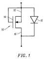
- the resulting structurehas a schematic as illustrated in FIG. 1 and comprises a plurality of rectifier elements or unit cells dispersed in a device region of a semiconductor body defined by a guard ring. Fabrication of the semiconductor rectifier device in accordance with the invention and using standard semiconductor processing techniques.
- the exposed polysilicon 36 and gate oxide 34is removed by etching using photoresist mask 38 , leaving the gate oxide 34 and doped polysilicon gate 36 under photoresist mask 38 .
- An N-type dopant such as arsenicis then implanted at 40 in the exposed semiconductor surface of sufficient concentration (E11-E14/cm 2 ) to form a good ohmic contact.
- the arsenicshould be about one order of magnitude lower than the BF 2 implant of FIG. 2C so that the net surface concentration in the guard ring and plug areas is still P+ with a value that is high enough to form a good P-type ohmic contact.
Landscapes
- Engineering & Computer Science (AREA)
- Physics & Mathematics (AREA)
- Condensed Matter Physics & Semiconductors (AREA)
- General Physics & Mathematics (AREA)
- Manufacturing & Machinery (AREA)
- Computer Hardware Design (AREA)
- Microelectronics & Electronic Packaging (AREA)
- Power Engineering (AREA)
- Electrodes Of Semiconductors (AREA)
- Insulated Gate Type Field-Effect Transistor (AREA)
Abstract
Description
Claims (17)
Priority Applications (8)
| Application Number | Priority Date | Filing Date | Title |
|---|---|---|---|
| US09/544,730US6448160B1 (en) | 1999-04-01 | 2000-04-06 | Method of fabricating power rectifier device to vary operating parameters and resulting device |
| US09/620,074US6399996B1 (en) | 1999-04-01 | 2000-07-20 | Schottky diode having increased active surface area and method of fabrication |
| US09/805,815US6420225B1 (en) | 1999-04-01 | 2001-03-13 | Method of fabricating power rectifier device |
| AU2001249231AAU2001249231A1 (en) | 2000-04-06 | 2001-03-15 | Method of fabricating power rectifier device to vary operating parameters and resulting device |
| CNB01800833XACN1201387C (en) | 2000-04-06 | 2001-03-15 | Method of making power rectifier device for varying operating parameters and device made therefrom |
| PCT/US2001/008494WO2001078134A1 (en) | 2000-04-06 | 2001-03-15 | Method of fabricating power rectifier device to vary operating parameters and resulting device |
| TW090107511ATW521435B (en) | 2000-04-06 | 2001-03-29 | Method of fabricating power rectifier device to vary operating parameters and resulting device |
| US10/238,104US6743703B2 (en) | 2000-04-06 | 2002-09-09 | Power diode having improved on resistance and breakdown voltage |
Applications Claiming Priority (2)
| Application Number | Priority Date | Filing Date | Title |
|---|---|---|---|
| US09/283,537US6331455B1 (en) | 1999-04-01 | 1999-04-01 | Power rectifier device and method of fabricating power rectifier devices |
| US09/544,730US6448160B1 (en) | 1999-04-01 | 2000-04-06 | Method of fabricating power rectifier device to vary operating parameters and resulting device |
Related Parent Applications (2)
| Application Number | Title | Priority Date | Filing Date |
|---|---|---|---|
| US09/283,537Continuation-In-PartUS6331455B1 (en) | 1999-04-01 | 1999-04-01 | Power rectifier device and method of fabricating power rectifier devices |
| US09/742,262DivisionUS6624030B2 (en) | 1999-04-01 | 2000-12-19 | Method of fabricating power rectifier device having a laterally graded P-N junction for a channel region |
Related Child Applications (3)
| Application Number | Title | Priority Date | Filing Date |
|---|---|---|---|
| US09/283,537DivisionUS6331455B1 (en) | 1999-04-01 | 1999-04-01 | Power rectifier device and method of fabricating power rectifier devices |
| US09/620,074Continuation-In-PartUS6399996B1 (en) | 1999-04-01 | 2000-07-20 | Schottky diode having increased active surface area and method of fabrication |
| US10/238,104Continuation-In-PartUS6743703B2 (en) | 2000-04-06 | 2002-09-09 | Power diode having improved on resistance and breakdown voltage |
Publications (1)
| Publication Number | Publication Date |
|---|---|
| US6448160B1true US6448160B1 (en) | 2002-09-10 |
Family
ID=24173345
Family Applications (2)
| Application Number | Title | Priority Date | Filing Date |
|---|---|---|---|
| US09/544,730Expired - LifetimeUS6448160B1 (en) | 1999-04-01 | 2000-04-06 | Method of fabricating power rectifier device to vary operating parameters and resulting device |
| US10/238,104Expired - LifetimeUS6743703B2 (en) | 2000-04-06 | 2002-09-09 | Power diode having improved on resistance and breakdown voltage |
Family Applications After (1)
| Application Number | Title | Priority Date | Filing Date |
|---|---|---|---|
| US10/238,104Expired - LifetimeUS6743703B2 (en) | 2000-04-06 | 2002-09-09 | Power diode having improved on resistance and breakdown voltage |
Country Status (5)
| Country | Link |
|---|---|
| US (2) | US6448160B1 (en) |
| CN (1) | CN1201387C (en) |
| AU (1) | AU2001249231A1 (en) |
| TW (1) | TW521435B (en) |
| WO (1) | WO2001078134A1 (en) |
Cited By (53)
| Publication number | Priority date | Publication date | Assignee | Title |
|---|---|---|---|---|
| US20020038891A1 (en)* | 2000-10-03 | 2002-04-04 | Sei-Hyung Ryu | Silicon carbide power metal-oxide semiconductor field effect transistors having a shorting channel and methods of fabricating silicon carbide metal-oxide semiconductor field effect transistors having a shorting channel |
| US20030006425A1 (en)* | 2000-02-22 | 2003-01-09 | International Rectifier Corporation | Manufacturing process and termination structure for fast recovery diode |
| US20030096464A1 (en)* | 2001-11-21 | 2003-05-22 | Frederic Lanois | Method for forming a schottky diode on a silicon carbide substrate |
| US6743703B2 (en) | 2000-04-06 | 2004-06-01 | Apd Semiconductor, Inc. | Power diode having improved on resistance and breakdown voltage |
| US20040119076A1 (en)* | 2002-12-20 | 2004-06-24 | Sei-Hyung Ryu | Vertical JFET limited silicon carbide power metal-oxide semiconductor field effect transistors and methods of fabricating vertical JFET limited silicon carbide metal- oxide semiconductor field effect transistors |
| US20040211980A1 (en)* | 2003-04-24 | 2004-10-28 | Sei-Hyung Ryu | Silicon carbide power devices with self-aligned source and well regions and methods of fabricating same |
| US20040212011A1 (en)* | 2003-04-24 | 2004-10-28 | Sei-Hyung Ryu | Silicon carbide mosfets with integrated antiparallel junction barrier schottky free wheeling diodes and methods of fabricating the same |
| US20050029614A1 (en)* | 2003-08-05 | 2005-02-10 | Chip Integration Tech Co., Ltd. | High switching speed two mask schottky diode with high field breakdown |
| US20050056889A1 (en)* | 2003-09-15 | 2005-03-17 | Gordon Ma | LDMOS transistor |
| US20060157815A1 (en)* | 2005-01-20 | 2006-07-20 | Apd Semiconductor, Inc. | Integrated circuit including power diode |
| US7118970B2 (en) | 2004-06-22 | 2006-10-10 | Cree, Inc. | Methods of fabricating silicon carbide devices with hybrid well regions |
| US20060261348A1 (en)* | 2005-05-18 | 2006-11-23 | Sei-Hyung Ryu | High voltage silicon carbide devices having bi-directional blocking capabilities and methods of fabricating the same |
| US20060261346A1 (en)* | 2005-05-18 | 2006-11-23 | Sei-Hyung Ryu | High voltage silicon carbide devices having bi-directional blocking capabilities and methods of fabricating the same |
| US20060261345A1 (en)* | 2005-05-18 | 2006-11-23 | Sei-Hyung Ryu | High voltage silicon carbide devices having bi-directional blocking capabilities and methods of fabricating the same |
| US7414268B2 (en) | 2005-05-18 | 2008-08-19 | Cree, Inc. | High voltage silicon carbide MOS-bipolar devices having bi-directional blocking capabilities |
| US20090078962A1 (en)* | 2007-09-26 | 2009-03-26 | Lakota Technologies, Inc. | Adjustable Field Effect Rectifier |
| US7528040B2 (en) | 2005-05-24 | 2009-05-05 | Cree, Inc. | Methods of fabricating silicon carbide devices having smooth channels |
| US20100244047A1 (en)* | 2009-03-27 | 2010-09-30 | Cree, Inc. | Methods of Forming Semiconductor Devices Including Epitaxial Layers and Related Structures |
| WO2010146264A2 (en) | 2009-06-15 | 2010-12-23 | Valeo Equipements Electriques Moteur | Alternators for automobiles provided with improved voltage-rectifying means |
| FR2952249A1 (en)* | 2009-11-03 | 2011-05-06 | Valeo Equip Electr Moteur | Electricity generating device for motor vehicle, has alternator comprising stator that is provided with stator windings, rotor provided with field coil, and rectification bridge contained in electronic case |
| US8193848B2 (en) | 2009-06-02 | 2012-06-05 | Cree, Inc. | Power switching devices having controllable surge current capabilities |
| US8294507B2 (en) | 2009-05-08 | 2012-10-23 | Cree, Inc. | Wide bandgap bipolar turn-off thyristor having non-negative temperature coefficient and related control circuits |
| US8330244B2 (en) | 2006-08-01 | 2012-12-11 | Cree, Inc. | Semiconductor devices including Schottky diodes having doped regions arranged as islands and methods of fabricating same |
| US8354690B2 (en) | 2009-08-31 | 2013-01-15 | Cree, Inc. | Solid-state pinch off thyristor circuits |
| CN102983177A (en)* | 2012-12-07 | 2013-03-20 | 杭州士兰集成电路有限公司 | Schottky diode and fabrication method thereof |
| US8415671B2 (en) | 2010-04-16 | 2013-04-09 | Cree, Inc. | Wide band-gap MOSFETs having a heterojunction under gate trenches thereof and related methods of forming such devices |
| US8421118B2 (en) | 2007-09-26 | 2013-04-16 | Stmicroelectronics N.V. | Regenerative building block and diode bridge rectifier and methods |
| US8432012B2 (en) | 2006-08-01 | 2013-04-30 | Cree, Inc. | Semiconductor devices including schottky diodes having overlapping doped regions and methods of fabricating same |
| US8541787B2 (en) | 2009-07-15 | 2013-09-24 | Cree, Inc. | High breakdown voltage wide band-gap MOS-gated bipolar junction transistors with avalanche capability |
| US8618582B2 (en) | 2011-09-11 | 2013-12-31 | Cree, Inc. | Edge termination structure employing recesses for edge termination elements |
| US8629509B2 (en) | 2009-06-02 | 2014-01-14 | Cree, Inc. | High voltage insulated gate bipolar transistors with minority carrier diverter |
| US8633521B2 (en) | 2007-09-26 | 2014-01-21 | Stmicroelectronics N.V. | Self-bootstrapping field effect diode structures and methods |
| US8643055B2 (en) | 2007-09-26 | 2014-02-04 | Stmicroelectronics N.V. | Series current limiter device |
| US8653534B2 (en) | 2008-05-21 | 2014-02-18 | Cree, Inc. | Junction Barrier Schottky diodes with current surge capability |
| US8664665B2 (en) | 2011-09-11 | 2014-03-04 | Cree, Inc. | Schottky diode employing recesses for elements of junction barrier array |
| US20140077302A1 (en)* | 2012-09-14 | 2014-03-20 | Electronics And Telecommunications Research Institute | Power rectifying devices |
| US8680587B2 (en) | 2011-09-11 | 2014-03-25 | Cree, Inc. | Schottky diode |
| US8710510B2 (en) | 2006-08-17 | 2014-04-29 | Cree, Inc. | High power insulated gate bipolar transistors |
| US20140197449A1 (en)* | 2013-01-14 | 2014-07-17 | Electronics And Telecommunications Research Institute | Semiconductor rectifier device |
| US8835987B2 (en) | 2007-02-27 | 2014-09-16 | Cree, Inc. | Insulated gate bipolar transistors including current suppressing layers |
| US20140273376A1 (en)* | 2013-03-15 | 2014-09-18 | Taiwan Semiconductor Manufacturing Company Limited | Semiconductor arrangement and formation thereof |
| US9018048B2 (en) | 2012-09-27 | 2015-04-28 | Stmicroelectronics S.R.L. | Process for manufactuirng super-barrier rectifiers |
| US9029945B2 (en) | 2011-05-06 | 2015-05-12 | Cree, Inc. | Field effect transistor devices with low source resistance |
| US9117739B2 (en) | 2010-03-08 | 2015-08-25 | Cree, Inc. | Semiconductor devices with heterojunction barrier regions and methods of fabricating same |
| US9142662B2 (en) | 2011-05-06 | 2015-09-22 | Cree, Inc. | Field effect transistor devices with low source resistance |
| US9252293B2 (en) | 2014-01-22 | 2016-02-02 | Alexei Ankoudinov | Trench field effect diodes and methods of manufacturing those diodes |
| US9324625B2 (en) | 2012-05-31 | 2016-04-26 | Infineon Technologies Ag | Gated diode, battery charging assembly and generator assembly |
| US9373617B2 (en) | 2011-09-11 | 2016-06-21 | Cree, Inc. | High current, low switching loss SiC power module |
| US9419116B2 (en) | 2014-01-22 | 2016-08-16 | Alexei Ankoudinov | Diodes and methods of manufacturing diodes |
| US9508846B2 (en) | 2014-04-18 | 2016-11-29 | Stmicroelectronics S.R.L. | Vertical MOS semiconductor device for high-frequency applications, and related manufacturing process |
| US9640617B2 (en) | 2011-09-11 | 2017-05-02 | Cree, Inc. | High performance power module |
| US9673283B2 (en) | 2011-05-06 | 2017-06-06 | Cree, Inc. | Power module for supporting high current densities |
| CN109285774A (en)* | 2018-09-12 | 2019-01-29 | 江苏能华微电子科技发展有限公司 | A gallium nitride-based junction barrier Schottky diode and method for forming the same |
Families Citing this family (30)
| Publication number | Priority date | Publication date | Assignee | Title |
|---|---|---|---|---|
| DE10201378A1 (en)* | 2002-01-16 | 2003-07-24 | Ixys Semiconductor Gmbh | Power semiconductor for a commutating branch has a recovery diode as a first semiconductor switch and a thyristor as a second semiconductor switch connected in parallel to the recovery diode. |
| JP4166627B2 (en)* | 2003-05-30 | 2008-10-15 | 株式会社デンソー | Semiconductor device |
| DE10355587B4 (en)* | 2003-11-28 | 2007-05-24 | Infineon Technologies Ag | Method of fabricating a vertical power semiconductor transistor |
| JP4536366B2 (en)* | 2003-12-22 | 2010-09-01 | 株式会社豊田中央研究所 | Semiconductor device and its design support program |
| US7078780B2 (en)* | 2004-04-19 | 2006-07-18 | Shye-Lin Wu | Schottky barrier diode and method of making the same |
| US20050242411A1 (en)* | 2004-04-29 | 2005-11-03 | Hsuan Tso | [superjunction schottky device and fabrication thereof] |
| EP1790013A1 (en)* | 2004-08-31 | 2007-05-30 | Freescale Semiconductor, Inc. | Power semiconductor device |
| US7928470B2 (en)* | 2005-11-25 | 2011-04-19 | Denso Corporation | Semiconductor device having super junction MOS transistor and method for manufacturing the same |
| US7777257B2 (en)* | 2007-02-14 | 2010-08-17 | Freescale Semiconductor, Inc. | Bipolar Schottky diode and method |
| US8217419B2 (en) | 2007-06-15 | 2012-07-10 | Rohm Co., Ltd. | Semiconductor device |
| US7888775B2 (en)* | 2007-09-27 | 2011-02-15 | Infineon Technologies Ag | Vertical diode using silicon formed by selective epitaxial growth |
| DE102007052202B3 (en)* | 2007-10-30 | 2008-11-13 | Infineon Technologies Austria Ag | Semiconductor component i.e. Schottky diode, has metallization structure electrically connected with compensation zones by Schottky contact and with drift zones by ohmic contact, where structure is arranged opposite to another structure |
| JP2010056510A (en)* | 2008-07-31 | 2010-03-11 | Nec Electronics Corp | Semiconductor device |
| CN101533804B (en)* | 2009-04-02 | 2011-09-14 | 英属维京群岛商节能元件股份有限公司 | A metal oxide semiconductor P-N junction schootky diode structure and the production method thereof |
| CN101510528B (en)* | 2009-04-02 | 2011-09-28 | 英属维京群岛商节能元件股份有限公司 | Metal Oxide Semiconductor P-N Junction Diode Structure and Manufacturing Method |
| US9230810B2 (en) | 2009-09-03 | 2016-01-05 | Vishay-Siliconix | System and method for substrate wafer back side and edge cross section seals |
| CN101699616B (en)* | 2009-10-23 | 2011-11-16 | 英属维京群岛商节能元件股份有限公司 | Trench MOS P-N Junction Schottky Diode Structure and Manufacturing Method |
| JP5672756B2 (en)* | 2010-04-16 | 2015-02-18 | サンケン電気株式会社 | Semiconductor device |
| JP6197294B2 (en)* | 2013-01-16 | 2017-09-20 | 富士電機株式会社 | Semiconductor element |
| TW201430957A (en)* | 2013-01-25 | 2014-08-01 | Anpec Electronics Corp | Semiconductor power device manufacturing method |
| CN104051344B (en)* | 2013-03-15 | 2017-05-10 | 台湾积体电路制造股份有限公司 | Semiconductor arrangement and formation thereof |
| CN103311274B (en)* | 2013-05-14 | 2016-03-23 | 深圳深爱半导体股份有限公司 | The semiconductor device of the non-aligned type super-junction structures of tool and manufacture method thereof |
| CN103325839A (en)* | 2013-06-26 | 2013-09-25 | 张家港凯思半导体有限公司 | MOS super barrier rectifier device and manufacturing method thereof |
| DE102013220011B4 (en)* | 2013-10-02 | 2025-01-02 | Robert Bosch Gmbh | Semiconductor device with temperature-compensated breakdown voltage |
| US9123557B2 (en)* | 2013-11-08 | 2015-09-01 | Sumpro Electronics Corporation | Fast recovery rectifier |
| CN104241126B (en)* | 2014-09-17 | 2017-10-31 | 中航(重庆)微电子有限公司 | Groove-shaped IGBT and preparation method |
| CN105529262A (en)* | 2014-09-29 | 2016-04-27 | 无锡华润华晶微电子有限公司 | Vertical double diffused metal oxide semiconductor field effect transistor and manufacturing method thereof |
| JP6846119B2 (en)* | 2016-05-02 | 2021-03-24 | 株式会社 日立パワーデバイス | Diode and power converter using it |
| CN107946371B (en)* | 2017-01-24 | 2024-04-05 | 重庆中科渝芯电子有限公司 | Super-barrier rectifier with Schottky barrier contact and manufacturing method thereof |
| CN115985956B (en)* | 2023-03-20 | 2023-06-13 | 苏州锴威特半导体股份有限公司 | Annular grid SiC MOSFET power device and manufacturing method |
Citations (23)
| Publication number | Priority date | Publication date | Assignee | Title |
|---|---|---|---|---|
| US3603811A (en) | 1969-12-09 | 1971-09-07 | American Optical Corp | Two-terminal bipolar self-powered low current limiter |
| US4373252A (en)* | 1981-02-17 | 1983-02-15 | Fairchild Camera & Instrument | Method for manufacturing a semiconductor structure having reduced lateral spacing between buried regions |
| EP0322040A2 (en)* | 1987-12-22 | 1989-06-28 | STMicroelectronics S.r.l. | Manufacturing process for a monolithic semiconductor device comprising at least one transistor of an integrated control circuit and one power transistor integrated on the same chip |
| US4982260A (en) | 1989-10-02 | 1991-01-01 | General Electric Company | Power rectifier with trenches |
| US4996581A (en)* | 1988-02-03 | 1991-02-26 | Kabushiki Kaisha Toshiba | Bipolar transistor |
| US5430315A (en) | 1993-07-22 | 1995-07-04 | Rumennik; Vladimir | Bi-directional power trench MOS field effect transistor having low on-state resistance and low leakage current |
| US5629536A (en) | 1995-11-21 | 1997-05-13 | Motorola, Inc. | High voltage current limiter and method for making |
| US5643809A (en)* | 1995-03-08 | 1997-07-01 | Integrated Device Technology, Inc. | Method for making high speed poly-emitter bipolar transistor |
| US5747841A (en) | 1994-12-20 | 1998-05-05 | U.S. Philips Corporation | Circuit arrangement, and junction field effect transistor suitable for use in such a circuit arrangement |
| US5818084A (en) | 1996-05-15 | 1998-10-06 | Siliconix Incorporated | Pseudo-Schottky diode |
| US5825079A (en) | 1997-01-23 | 1998-10-20 | Luminous Intent, Inc. | Semiconductor diodes having low forward conduction voltage drop and low reverse current leakage |
| US5869380A (en)* | 1998-07-06 | 1999-02-09 | Industrial Technology Research Institute | Method for forming a bipolar junction transistor |
| US5877515A (en) | 1995-10-10 | 1999-03-02 | International Rectifier Corporation | SiC semiconductor device |
| US5956582A (en) | 1993-05-10 | 1999-09-21 | Sgs-Thomson Microelectronics S.A. | Current limiting circuit with continuous metallization |
| US6034385A (en) | 1995-12-22 | 2000-03-07 | Siemens Aktiengesellschaft | Current-limiting semiconductor configuration |
| US6097046A (en) | 1993-04-30 | 2000-08-01 | Texas Instruments Incorporated | Vertical field effect transistor and diode |
| US6186408B1 (en) | 1999-05-28 | 2001-02-13 | Advanced Power Devices, Inc. | High cell density power rectifier |
| US6225180B1 (en)* | 1998-01-16 | 2001-05-01 | Mitsubishi Denki Kabushiki Kaisha | Semiconductor device and method of manufacturing the same |
| US6235601B1 (en)* | 1995-12-28 | 2001-05-22 | Philips Electronics North America Corporation | Method of manufacturing a self-aligned vertical bipolar transistor |
| US6258634B1 (en)* | 1998-06-19 | 2001-07-10 | National Semiconductor Corporation | Method for manufacturing a dual-direction over-voltage and over-current IC protection device and its cell structure |
| US6313001B1 (en)* | 1998-11-04 | 2001-11-06 | Telefonaktiebolaget Lm Ericsson (Publ) | Method for semiconductor manufacturing |
| US6323091B1 (en)* | 1999-07-16 | 2001-11-27 | Zilog, Inc. | Method of forming semiconductor memory device with LDD |
| US6362036B1 (en)* | 1998-02-10 | 2002-03-26 | Stmicroelectronics S.R.L. | VDMOS transistor protected against over-voltages between source and gate |
Family Cites Families (11)
| Publication number | Priority date | Publication date | Assignee | Title |
|---|---|---|---|---|
| GB2089119A (en) | 1980-12-10 | 1982-06-16 | Philips Electronic Associated | High voltage semiconductor devices |
| JP3321185B2 (en)* | 1990-09-28 | 2002-09-03 | 株式会社東芝 | High voltage semiconductor device |
| CN1019720B (en) | 1991-03-19 | 1992-12-30 | 电子科技大学 | Power semiconductor device |
| DE4309764C2 (en) | 1993-03-25 | 1997-01-30 | Siemens Ag | Power MOSFET |
| US5594261A (en)* | 1994-04-05 | 1997-01-14 | Harris Corporation | Device for isolating parallel sub-elements with reverse conducting diode regions |
| US5969400A (en)* | 1995-03-15 | 1999-10-19 | Kabushiki Kaisha Toshiba | High withstand voltage semiconductor device |
| US5886383A (en)* | 1997-01-10 | 1999-03-23 | International Rectifier Corporation | Integrated schottky diode and mosgated device |
| US6081009A (en) | 1997-11-10 | 2000-06-27 | Intersil Corporation | High voltage mosfet structure |
| DE19839970C2 (en) | 1998-09-02 | 2000-11-02 | Siemens Ag | Edge structure and drift area for a semiconductor component and method for their production |
| US6037631A (en) | 1998-09-18 | 2000-03-14 | Siemens Aktiengesellschaft | Semiconductor component with a high-voltage endurance edge structure |
| US6448160B1 (en) | 1999-04-01 | 2002-09-10 | Apd Semiconductor, Inc. | Method of fabricating power rectifier device to vary operating parameters and resulting device |
- 2000
- 2000-04-06USUS09/544,730patent/US6448160B1/ennot_activeExpired - Lifetime
- 2001
- 2001-03-15WOPCT/US2001/008494patent/WO2001078134A1/enactiveApplication Filing
- 2001-03-15CNCNB01800833XApatent/CN1201387C/ennot_activeExpired - Fee Related
- 2001-03-15AUAU2001249231Apatent/AU2001249231A1/ennot_activeAbandoned
- 2001-03-29TWTW090107511Apatent/TW521435B/ennot_activeIP Right Cessation
- 2002
- 2002-09-09USUS10/238,104patent/US6743703B2/ennot_activeExpired - Lifetime
Patent Citations (24)
| Publication number | Priority date | Publication date | Assignee | Title |
|---|---|---|---|---|
| US3603811A (en) | 1969-12-09 | 1971-09-07 | American Optical Corp | Two-terminal bipolar self-powered low current limiter |
| US4373252A (en)* | 1981-02-17 | 1983-02-15 | Fairchild Camera & Instrument | Method for manufacturing a semiconductor structure having reduced lateral spacing between buried regions |
| EP0322040A2 (en)* | 1987-12-22 | 1989-06-28 | STMicroelectronics S.r.l. | Manufacturing process for a monolithic semiconductor device comprising at least one transistor of an integrated control circuit and one power transistor integrated on the same chip |
| US4996581A (en)* | 1988-02-03 | 1991-02-26 | Kabushiki Kaisha Toshiba | Bipolar transistor |
| US4982260A (en) | 1989-10-02 | 1991-01-01 | General Electric Company | Power rectifier with trenches |
| US6097046A (en) | 1993-04-30 | 2000-08-01 | Texas Instruments Incorporated | Vertical field effect transistor and diode |
| US5956582A (en) | 1993-05-10 | 1999-09-21 | Sgs-Thomson Microelectronics S.A. | Current limiting circuit with continuous metallization |
| US5430315A (en) | 1993-07-22 | 1995-07-04 | Rumennik; Vladimir | Bi-directional power trench MOS field effect transistor having low on-state resistance and low leakage current |
| US5747841A (en) | 1994-12-20 | 1998-05-05 | U.S. Philips Corporation | Circuit arrangement, and junction field effect transistor suitable for use in such a circuit arrangement |
| US5643809A (en)* | 1995-03-08 | 1997-07-01 | Integrated Device Technology, Inc. | Method for making high speed poly-emitter bipolar transistor |
| US5877515A (en) | 1995-10-10 | 1999-03-02 | International Rectifier Corporation | SiC semiconductor device |
| US5751025A (en) | 1995-11-21 | 1998-05-12 | Motorola, Inc. | High voltage current limiter and method for making |
| US5629536A (en) | 1995-11-21 | 1997-05-13 | Motorola, Inc. | High voltage current limiter and method for making |
| US6034385A (en) | 1995-12-22 | 2000-03-07 | Siemens Aktiengesellschaft | Current-limiting semiconductor configuration |
| US6235601B1 (en)* | 1995-12-28 | 2001-05-22 | Philips Electronics North America Corporation | Method of manufacturing a self-aligned vertical bipolar transistor |
| US5818084A (en) | 1996-05-15 | 1998-10-06 | Siliconix Incorporated | Pseudo-Schottky diode |
| US5825079A (en) | 1997-01-23 | 1998-10-20 | Luminous Intent, Inc. | Semiconductor diodes having low forward conduction voltage drop and low reverse current leakage |
| US6225180B1 (en)* | 1998-01-16 | 2001-05-01 | Mitsubishi Denki Kabushiki Kaisha | Semiconductor device and method of manufacturing the same |
| US6362036B1 (en)* | 1998-02-10 | 2002-03-26 | Stmicroelectronics S.R.L. | VDMOS transistor protected against over-voltages between source and gate |
| US6258634B1 (en)* | 1998-06-19 | 2001-07-10 | National Semiconductor Corporation | Method for manufacturing a dual-direction over-voltage and over-current IC protection device and its cell structure |
| US5869380A (en)* | 1998-07-06 | 1999-02-09 | Industrial Technology Research Institute | Method for forming a bipolar junction transistor |
| US6313001B1 (en)* | 1998-11-04 | 2001-11-06 | Telefonaktiebolaget Lm Ericsson (Publ) | Method for semiconductor manufacturing |
| US6186408B1 (en) | 1999-05-28 | 2001-02-13 | Advanced Power Devices, Inc. | High cell density power rectifier |
| US6323091B1 (en)* | 1999-07-16 | 2001-11-27 | Zilog, Inc. | Method of forming semiconductor memory device with LDD |
Non-Patent Citations (1)
| Title |
|---|
| Christiansen, Bob, "Synchronous Rectification Improves with Age," PCIM, Aug., 1998, 6 pp. |
Cited By (99)
| Publication number | Priority date | Publication date | Assignee | Title |
|---|---|---|---|---|
| US20030006425A1 (en)* | 2000-02-22 | 2003-01-09 | International Rectifier Corporation | Manufacturing process and termination structure for fast recovery diode |
| US6699775B2 (en)* | 2000-02-22 | 2004-03-02 | International Rectifier Corporation | Manufacturing process for fast recovery diode |
| US6743703B2 (en) | 2000-04-06 | 2004-06-01 | Apd Semiconductor, Inc. | Power diode having improved on resistance and breakdown voltage |
| US6956238B2 (en) | 2000-10-03 | 2005-10-18 | Cree, Inc. | Silicon carbide power metal-oxide semiconductor field effect transistors having a shorting channel and methods of fabricating silicon carbide metal-oxide semiconductor field effect transistors having a shorting channel |
| US20020038891A1 (en)* | 2000-10-03 | 2002-04-04 | Sei-Hyung Ryu | Silicon carbide power metal-oxide semiconductor field effect transistors having a shorting channel and methods of fabricating silicon carbide metal-oxide semiconductor field effect transistors having a shorting channel |
| US20030096464A1 (en)* | 2001-11-21 | 2003-05-22 | Frederic Lanois | Method for forming a schottky diode on a silicon carbide substrate |
| US7101739B2 (en)* | 2001-11-21 | 2006-09-05 | Stmicroelectronics S.A. | Method for forming a schottky diode on a silicon carbide substrate |
| US20040119076A1 (en)* | 2002-12-20 | 2004-06-24 | Sei-Hyung Ryu | Vertical JFET limited silicon carbide power metal-oxide semiconductor field effect transistors and methods of fabricating vertical JFET limited silicon carbide metal- oxide semiconductor field effect transistors |
| US8492827B2 (en) | 2002-12-20 | 2013-07-23 | Cree, Inc. | Vertical JFET limited silicon carbide metal-oxide semiconductor field effect transistors |
| US20070158658A1 (en)* | 2002-12-20 | 2007-07-12 | Cree, Inc. | Methods of fabricating vertical jfet limited silicon carbide metal-oxide semiconductor field effect transistors |
| US7923320B2 (en) | 2002-12-20 | 2011-04-12 | Cree, Inc. | Methods of fabricating vertical JFET limited silicon carbide metal-oxide semiconductor field effect transistors |
| US7221010B2 (en) | 2002-12-20 | 2007-05-22 | Cree, Inc. | Vertical JFET limited silicon carbide power metal-oxide semiconductor field effect transistors |
| US6979863B2 (en) | 2003-04-24 | 2005-12-27 | Cree, Inc. | Silicon carbide MOSFETs with integrated antiparallel junction barrier Schottky free wheeling diodes and methods of fabricating the same |
| US7074643B2 (en) | 2003-04-24 | 2006-07-11 | Cree, Inc. | Silicon carbide power devices with self-aligned source and well regions and methods of fabricating same |
| US20040211980A1 (en)* | 2003-04-24 | 2004-10-28 | Sei-Hyung Ryu | Silicon carbide power devices with self-aligned source and well regions and methods of fabricating same |
| US20060237728A1 (en)* | 2003-04-24 | 2006-10-26 | Sei-Hyung Ryu | Silicon carbide power devices with self-aligned source and well regions |
| US20040212011A1 (en)* | 2003-04-24 | 2004-10-28 | Sei-Hyung Ryu | Silicon carbide mosfets with integrated antiparallel junction barrier schottky free wheeling diodes and methods of fabricating the same |
| US7381992B2 (en) | 2003-04-24 | 2008-06-03 | Cree, Inc. | Silicon carbide power devices with self-aligned source and well regions |
| US6998694B2 (en)* | 2003-08-05 | 2006-02-14 | Shye-Lin Wu | High switching speed two mask Schottky diode with high field breakdown |
| US20050029614A1 (en)* | 2003-08-05 | 2005-02-10 | Chip Integration Tech Co., Ltd. | High switching speed two mask schottky diode with high field breakdown |
| US7049669B2 (en)* | 2003-09-15 | 2006-05-23 | Infineon Technologies Ag | LDMOS transistor |
| US20050056889A1 (en)* | 2003-09-15 | 2005-03-17 | Gordon Ma | LDMOS transistor |
| US20060289874A1 (en)* | 2004-06-22 | 2006-12-28 | Das Mrinal K | Silicon carbide devices with hybrid well regions |
| US7705362B2 (en) | 2004-06-22 | 2010-04-27 | Cree, Inc. | Silicon carbide devices with hybrid well regions |
| US7118970B2 (en) | 2004-06-22 | 2006-10-10 | Cree, Inc. | Methods of fabricating silicon carbide devices with hybrid well regions |
| JP2008529279A (en)* | 2005-01-20 | 2008-07-31 | ダイオデス・インコーポレーテッド | Integrated circuit including power diode |
| US20060157815A1 (en)* | 2005-01-20 | 2006-07-20 | Apd Semiconductor, Inc. | Integrated circuit including power diode |
| US7250668B2 (en) | 2005-01-20 | 2007-07-31 | Diodes, Inc. | Integrated circuit including power diode |
| US7964933B2 (en) | 2005-01-20 | 2011-06-21 | Diodes Inc. | Integrated circuit including power diode |
| US20070246794A1 (en)* | 2005-01-20 | 2007-10-25 | Paul Chang | Integrated circuit including power diode |
| US7615801B2 (en) | 2005-05-18 | 2009-11-10 | Cree, Inc. | High voltage silicon carbide devices having bi-directional blocking capabilities |
| US20060261346A1 (en)* | 2005-05-18 | 2006-11-23 | Sei-Hyung Ryu | High voltage silicon carbide devices having bi-directional blocking capabilities and methods of fabricating the same |
| US7391057B2 (en) | 2005-05-18 | 2008-06-24 | Cree, Inc. | High voltage silicon carbide devices having bi-directional blocking capabilities |
| US7414268B2 (en) | 2005-05-18 | 2008-08-19 | Cree, Inc. | High voltage silicon carbide MOS-bipolar devices having bi-directional blocking capabilities |
| US20060261345A1 (en)* | 2005-05-18 | 2006-11-23 | Sei-Hyung Ryu | High voltage silicon carbide devices having bi-directional blocking capabilities and methods of fabricating the same |
| US20060261348A1 (en)* | 2005-05-18 | 2006-11-23 | Sei-Hyung Ryu | High voltage silicon carbide devices having bi-directional blocking capabilities and methods of fabricating the same |
| US8859366B2 (en) | 2005-05-24 | 2014-10-14 | Cree, Inc. | Methods of fabricating silicon carbide devices having smooth channels |
| US9142663B2 (en) | 2005-05-24 | 2015-09-22 | Cree, Inc. | Silicon carbide devices having smooth channels |
| US20090261351A1 (en)* | 2005-05-24 | 2009-10-22 | Cree, Inc. | Silicon Carbide Devices Having Smooth Channels |
| US7528040B2 (en) | 2005-05-24 | 2009-05-05 | Cree, Inc. | Methods of fabricating silicon carbide devices having smooth channels |
| US8188483B2 (en) | 2005-05-24 | 2012-05-29 | Cree, Inc. | Silicon carbide devices having smooth channels |
| US8432012B2 (en) | 2006-08-01 | 2013-04-30 | Cree, Inc. | Semiconductor devices including schottky diodes having overlapping doped regions and methods of fabricating same |
| US8330244B2 (en) | 2006-08-01 | 2012-12-11 | Cree, Inc. | Semiconductor devices including Schottky diodes having doped regions arranged as islands and methods of fabricating same |
| US9548374B2 (en) | 2006-08-17 | 2017-01-17 | Cree, Inc. | High power insulated gate bipolar transistors |
| US8710510B2 (en) | 2006-08-17 | 2014-04-29 | Cree, Inc. | High power insulated gate bipolar transistors |
| US9064840B2 (en) | 2007-02-27 | 2015-06-23 | Cree, Inc. | Insulated gate bipolar transistors including current suppressing layers |
| US8835987B2 (en) | 2007-02-27 | 2014-09-16 | Cree, Inc. | Insulated gate bipolar transistors including current suppressing layers |
| US9048308B2 (en) | 2007-09-26 | 2015-06-02 | Stmicroelectronics International N.V. | Regenerative building block and diode bridge rectifier and methods |
| US8633521B2 (en) | 2007-09-26 | 2014-01-21 | Stmicroelectronics N.V. | Self-bootstrapping field effect diode structures and methods |
| US9029921B2 (en) | 2007-09-26 | 2015-05-12 | Stmicroelectronics International N.V. | Self-bootstrapping field effect diode structures and methods |
| US8421118B2 (en) | 2007-09-26 | 2013-04-16 | Stmicroelectronics N.V. | Regenerative building block and diode bridge rectifier and methods |
| US9012954B2 (en) | 2007-09-26 | 2015-04-21 | STMicroelectronics International B.V. | Adjustable field effect rectifier |
| US8148748B2 (en) | 2007-09-26 | 2012-04-03 | Stmicroelectronics N.V. | Adjustable field effect rectifier |
| US20090078962A1 (en)* | 2007-09-26 | 2009-03-26 | Lakota Technologies, Inc. | Adjustable Field Effect Rectifier |
| US8598620B2 (en) | 2007-09-26 | 2013-12-03 | Stmicroelectronics N.V. | MOSFET with integrated field effect rectifier |
| US8643055B2 (en) | 2007-09-26 | 2014-02-04 | Stmicroelectronics N.V. | Series current limiter device |
| US8653534B2 (en) | 2008-05-21 | 2014-02-18 | Cree, Inc. | Junction Barrier Schottky diodes with current surge capability |
| US9640652B2 (en) | 2009-03-27 | 2017-05-02 | Cree, Inc. | Semiconductor devices including epitaxial layers and related methods |
| US8288220B2 (en) | 2009-03-27 | 2012-10-16 | Cree, Inc. | Methods of forming semiconductor devices including epitaxial layers and related structures |
| US20100244047A1 (en)* | 2009-03-27 | 2010-09-30 | Cree, Inc. | Methods of Forming Semiconductor Devices Including Epitaxial Layers and Related Structures |
| US8294507B2 (en) | 2009-05-08 | 2012-10-23 | Cree, Inc. | Wide bandgap bipolar turn-off thyristor having non-negative temperature coefficient and related control circuits |
| US8629509B2 (en) | 2009-06-02 | 2014-01-14 | Cree, Inc. | High voltage insulated gate bipolar transistors with minority carrier diverter |
| US8193848B2 (en) | 2009-06-02 | 2012-06-05 | Cree, Inc. | Power switching devices having controllable surge current capabilities |
| WO2010146264A2 (en) | 2009-06-15 | 2010-12-23 | Valeo Equipements Electriques Moteur | Alternators for automobiles provided with improved voltage-rectifying means |
| US8541787B2 (en) | 2009-07-15 | 2013-09-24 | Cree, Inc. | High breakdown voltage wide band-gap MOS-gated bipolar junction transistors with avalanche capability |
| US8354690B2 (en) | 2009-08-31 | 2013-01-15 | Cree, Inc. | Solid-state pinch off thyristor circuits |
| FR2952249A1 (en)* | 2009-11-03 | 2011-05-06 | Valeo Equip Electr Moteur | Electricity generating device for motor vehicle, has alternator comprising stator that is provided with stator windings, rotor provided with field coil, and rectification bridge contained in electronic case |
| US9595618B2 (en) | 2010-03-08 | 2017-03-14 | Cree, Inc. | Semiconductor devices with heterojunction barrier regions and methods of fabricating same |
| US9117739B2 (en) | 2010-03-08 | 2015-08-25 | Cree, Inc. | Semiconductor devices with heterojunction barrier regions and methods of fabricating same |
| US8415671B2 (en) | 2010-04-16 | 2013-04-09 | Cree, Inc. | Wide band-gap MOSFETs having a heterojunction under gate trenches thereof and related methods of forming such devices |
| US9142662B2 (en) | 2011-05-06 | 2015-09-22 | Cree, Inc. | Field effect transistor devices with low source resistance |
| US9029945B2 (en) | 2011-05-06 | 2015-05-12 | Cree, Inc. | Field effect transistor devices with low source resistance |
| US9673283B2 (en) | 2011-05-06 | 2017-06-06 | Cree, Inc. | Power module for supporting high current densities |
| US8664665B2 (en) | 2011-09-11 | 2014-03-04 | Cree, Inc. | Schottky diode employing recesses for elements of junction barrier array |
| US10153364B2 (en) | 2011-09-11 | 2018-12-11 | Cree, Inc. | Power module having a switch module for supporting high current densities |
| US11171229B2 (en) | 2011-09-11 | 2021-11-09 | Cree, Inc. | Low switching loss high performance power module |
| US11024731B2 (en) | 2011-09-11 | 2021-06-01 | Cree, Inc. | Power module for supporting high current densities |
| US9231122B2 (en) | 2011-09-11 | 2016-01-05 | Cree, Inc. | Schottky diode |
| US10141302B2 (en) | 2011-09-11 | 2018-11-27 | Cree, Inc. | High current, low switching loss SiC power module |
| US9865750B2 (en) | 2011-09-11 | 2018-01-09 | Cree, Inc. | Schottky diode |
| US9373617B2 (en) | 2011-09-11 | 2016-06-21 | Cree, Inc. | High current, low switching loss SiC power module |
| US8618582B2 (en) | 2011-09-11 | 2013-12-31 | Cree, Inc. | Edge termination structure employing recesses for edge termination elements |
| US9640617B2 (en) | 2011-09-11 | 2017-05-02 | Cree, Inc. | High performance power module |
| US8680587B2 (en) | 2011-09-11 | 2014-03-25 | Cree, Inc. | Schottky diode |
| US9324625B2 (en) | 2012-05-31 | 2016-04-26 | Infineon Technologies Ag | Gated diode, battery charging assembly and generator assembly |
| US10879384B2 (en) | 2012-05-31 | 2020-12-29 | Infineon Technologies Ag | Alternator assembly having a gated diode arranged in a load path between an input terminal and an output terminal |
| US10276706B2 (en) | 2012-05-31 | 2019-04-30 | Infineon Technologies Ag | Gated diode in a press-fit housing and an alternator assembly having a gated diode arranged in a load path |
| US20140077302A1 (en)* | 2012-09-14 | 2014-03-20 | Electronics And Telecommunications Research Institute | Power rectifying devices |
| US9018048B2 (en) | 2012-09-27 | 2015-04-28 | Stmicroelectronics S.R.L. | Process for manufactuirng super-barrier rectifiers |
| CN102983177A (en)* | 2012-12-07 | 2013-03-20 | 杭州士兰集成电路有限公司 | Schottky diode and fabrication method thereof |
| CN102983177B (en)* | 2012-12-07 | 2016-12-21 | 杭州士兰集成电路有限公司 | Schottky diode and preparation method thereof |
| US20140197449A1 (en)* | 2013-01-14 | 2014-07-17 | Electronics And Telecommunications Research Institute | Semiconductor rectifier device |
| US9437494B2 (en)* | 2013-03-15 | 2016-09-06 | Taiwan Semiconductor Manufacturing Company Limited | Semiconductor arrangement and formation thereof |
| US20140273376A1 (en)* | 2013-03-15 | 2014-09-18 | Taiwan Semiconductor Manufacturing Company Limited | Semiconductor arrangement and formation thereof |
| US9419116B2 (en) | 2014-01-22 | 2016-08-16 | Alexei Ankoudinov | Diodes and methods of manufacturing diodes |
| US9252293B2 (en) | 2014-01-22 | 2016-02-02 | Alexei Ankoudinov | Trench field effect diodes and methods of manufacturing those diodes |
| US9508846B2 (en) | 2014-04-18 | 2016-11-29 | Stmicroelectronics S.R.L. | Vertical MOS semiconductor device for high-frequency applications, and related manufacturing process |
| CN109285774A (en)* | 2018-09-12 | 2019-01-29 | 江苏能华微电子科技发展有限公司 | A gallium nitride-based junction barrier Schottky diode and method for forming the same |
| CN109285774B (en)* | 2018-09-12 | 2023-03-24 | 江苏能华微电子科技发展有限公司 | Junction barrier Schottky diode based on gallium nitride and forming method thereof |
Also Published As
| Publication number | Publication date |
|---|---|
| CN1201387C (en) | 2005-05-11 |
| US6743703B2 (en) | 2004-06-01 |
| WO2001078134A1 (en) | 2001-10-18 |
| CN1366710A (en) | 2002-08-28 |
| AU2001249231A1 (en) | 2001-10-23 |
| US20030006473A1 (en) | 2003-01-09 |
| TW521435B (en) | 2003-02-21 |
Similar Documents
| Publication | Publication Date | Title |
|---|---|---|
| US6448160B1 (en) | Method of fabricating power rectifier device to vary operating parameters and resulting device | |
| US6765264B1 (en) | Method of fabricating power rectifier device to vary operating parameters and resulting device | |
| US6420225B1 (en) | Method of fabricating power rectifier device | |
| US6426541B2 (en) | Schottky diode having increased forward current with improved reverse bias characteristics and method of fabrication | |
| JP3202021B2 (en) | Punch-through field-effect transistor | |
| US6404033B1 (en) | Schottky diode having increased active surface area with improved reverse bias characteristics and method of fabrication | |
| US5897343A (en) | Method of making a power switching trench MOSFET having aligned source regions | |
| US7696571B2 (en) | Method of manufacturing a trench transistor having a heavy body region | |
| US6399996B1 (en) | Schottky diode having increased active surface area and method of fabrication | |
| US6621107B2 (en) | Trench DMOS transistor with embedded trench schottky rectifier | |
| US9466710B2 (en) | Source and body contact structure for trench-DMOS devices using polysilicon | |
| US6979861B2 (en) | Power device having reduced reverse bias leakage current | |
| US6852597B2 (en) | Method for fabricating power semiconductor device having trench gate structure | |
| JP3717195B2 (en) | Power MOSFET and manufacturing method thereof | |
| EP0747966B1 (en) | High efficiency quasi-vertical DMOS in MOS or BICMOS process | |
| KR101955055B1 (en) | Power semiconductor device and method of fabricating the same | |
| JP2008529279A (en) | Integrated circuit including power diode | |
| KR20180097510A (en) | A source-gate region structure in a vertical power semiconductor device | |
| CN113540243B (en) | Avalanche protection transistor using bottom breakdown current path and method of forming the same | |
| JP5036130B2 (en) | Self-aligned vertical gate semiconductor device. | |
| US6515330B1 (en) | Power device having vertical current path with enhanced pinch-off for current limiting | |
| US7517759B2 (en) | Method of fabricating metal oxide semiconductor device | |
| US10032937B2 (en) | Monolithic series switching semiconductor device having low-resistance substrate contact structure and method | |
| US6107127A (en) | Method of making shallow well MOSFET structure | |
| US20240355872A1 (en) | Transistors with field-shield contacts and base contacts |
Legal Events
| Date | Code | Title | Description |
|---|---|---|---|
| AS | Assignment | Owner name:ADVANCED POWER DEVICES, CALIFORNIA Free format text:ASSIGNMENT OF ASSIGNORS INTEREST;ASSIGNORS:CHANG, PAUL;CHERN, GEENG-CHUAN;HSUEH, WAYNE Y.W.;AND OTHERS;REEL/FRAME:011175/0033;SIGNING DATES FROM 20000706 TO 20000717 | |
| AS | Assignment | Owner name:APD SEMICONDUCTOR, INC., CALIFORNIA Free format text:CHANGE OF NAME;ASSIGNOR:ADVANCED POWER DEVICES;REEL/FRAME:012768/0285 Effective date:20010928 | |
| STCF | Information on status: patent grant | Free format text:PATENTED CASE | |
| FEPP | Fee payment procedure | Free format text:PAYOR NUMBER ASSIGNED (ORIGINAL EVENT CODE: ASPN); ENTITY STATUS OF PATENT OWNER: LARGE ENTITY | |
| REMI | Maintenance fee reminder mailed | ||
| FPAY | Fee payment | Year of fee payment:4 | |
| SULP | Surcharge for late payment | ||
| AS | Assignment | Owner name:DIODES, INC., CALIFORNIA Free format text:ASSIGNMENT OF ASSIGNORS INTEREST;ASSIGNOR:APD SEMICONDUCTOR, INC.;REEL/FRAME:018552/0780 Effective date:20061031 | |
| FEPP | Fee payment procedure | Free format text:PAYER NUMBER DE-ASSIGNED (ORIGINAL EVENT CODE: RMPN); ENTITY STATUS OF PATENT OWNER: LARGE ENTITY Free format text:PAYOR NUMBER ASSIGNED (ORIGINAL EVENT CODE: ASPN); ENTITY STATUS OF PATENT OWNER: LARGE ENTITY | |
| FPAY | Fee payment | Year of fee payment:8 | |
| FEPP | Fee payment procedure | Free format text:PAYER NUMBER DE-ASSIGNED (ORIGINAL EVENT CODE: RMPN); ENTITY STATUS OF PATENT OWNER: LARGE ENTITY Free format text:PAYOR NUMBER ASSIGNED (ORIGINAL EVENT CODE: ASPN); ENTITY STATUS OF PATENT OWNER: LARGE ENTITY | |
| FEPP | Fee payment procedure | Free format text:PAYER NUMBER DE-ASSIGNED (ORIGINAL EVENT CODE: RMPN); ENTITY STATUS OF PATENT OWNER: LARGE ENTITY Free format text:PAYOR NUMBER ASSIGNED (ORIGINAL EVENT CODE: ASPN); ENTITY STATUS OF PATENT OWNER: LARGE ENTITY | |
| AS | Assignment | Owner name:BANK OF AMERICA, N.A., AS ADMINISTRATIVE AGENT, TE Free format text:SECURITY AGREEMENT;ASSIGNOR:DIODES INCORPORATED, AS GRANTOR;REEL/FRAME:029594/0472 Effective date:20130108 | |
| FEPP | Fee payment procedure | Free format text:PAT HOLDER NO LONGER CLAIMS SMALL ENTITY STATUS, ENTITY STATUS SET TO UNDISCOUNTED (ORIGINAL EVENT CODE: STOL); ENTITY STATUS OF PATENT OWNER: LARGE ENTITY | |
| FPAY | Fee payment | Year of fee payment:12 | |
| SULP | Surcharge for late payment |