US6447604B1 - Method for achieving improved epitaxy quality (surface texture and defect density) on free-standing (aluminum, indium, gallium) nitride ((al,in,ga)n) substrates for opto-electronic and electronic devices - Google Patents
Method for achieving improved epitaxy quality (surface texture and defect density) on free-standing (aluminum, indium, gallium) nitride ((al,in,ga)n) substrates for opto-electronic and electronic devicesDownload PDFInfo
- Publication number
- US6447604B1 US6447604B1US09/605,195US60519500AUS6447604B1US 6447604 B1US6447604 B1US 6447604B1US 60519500 AUS60519500 AUS 60519500AUS 6447604 B1US6447604 B1US 6447604B1
- Authority
- US
- United States
- Prior art keywords
- iii
- substrate
- nitride
- gan
- growth
- Prior art date
- Legal status (The legal status is an assumption and is not a legal conclusion. Google has not performed a legal analysis and makes no representation as to the accuracy of the status listed.)
- Expired - Lifetime
Links
- 239000000758substrateSubstances0.000titleclaimsabstractdescription455
- 238000000034methodMethods0.000titleclaimsabstractdescription274
- 150000004767nitridesChemical class0.000titleclaimsabstractdescription115
- 230000007547defectEffects0.000titleclaimsdescription76
- 229910052738indiumInorganic materials0.000titleclaimsdescription76
- 229910052733galliumInorganic materials0.000titleclaimsdescription75
- 230000001976improved effectEffects0.000titleclaimsdescription17
- 238000000407epitaxyMethods0.000titledescription29
- 230000005693optoelectronicsEffects0.000titledescription7
- 229910052782aluminiumInorganic materials0.000titledescription6
- APFVFJFRJDLVQX-UHFFFAOYSA-Nindium atomChemical compound[In]APFVFJFRJDLVQX-UHFFFAOYSA-N0.000titledescription4
- GYHNNYVSQQEPJS-UHFFFAOYSA-NGalliumChemical compound[Ga]GYHNNYVSQQEPJS-UHFFFAOYSA-N0.000title1
- XAGFODPZIPBFFR-UHFFFAOYSA-NaluminiumChemical compound[Al]XAGFODPZIPBFFR-UHFFFAOYSA-N0.000title1
- 230000012010growthEffects0.000claimsabstractdescription378
- 239000000463materialSubstances0.000claimsabstractdescription233
- 230000008569processEffects0.000claimsabstractdescription102
- 238000000151depositionMethods0.000claimsabstractdescription89
- IJGRMHOSHXDMSA-UHFFFAOYSA-NAtomic nitrogenChemical compoundN#NIJGRMHOSHXDMSA-UHFFFAOYSA-N0.000claimsabstractdescription82
- 229910052757nitrogenInorganic materials0.000claimsabstractdescription45
- 230000036961partial effectEffects0.000claimsabstractdescription25
- 239000010410layerSubstances0.000claimsdescription214
- 239000012535impuritySubstances0.000claimsdescription75
- 238000009499grossingMethods0.000claimsdescription71
- QGZKDVFQNNGYKY-UHFFFAOYSA-NAmmoniaChemical compoundNQGZKDVFQNNGYKY-UHFFFAOYSA-N0.000claimsdescription42
- 239000011229interlayerSubstances0.000claimsdescription42
- 238000004140cleaningMethods0.000claimsdescription41
- 230000008021depositionEffects0.000claimsdescription30
- 230000000694effectsEffects0.000claimsdescription27
- 238000001704evaporationMethods0.000claimsdescription26
- 238000000927vapour-phase epitaxyMethods0.000claimsdescription24
- 230000008020evaporationEffects0.000claimsdescription22
- 239000000203mixtureSubstances0.000claimsdescription22
- 238000005498polishingMethods0.000claimsdescription18
- 239000004094surface-active agentSubstances0.000claimsdescription18
- 230000015572biosynthetic processEffects0.000claimsdescription16
- 230000006911nucleationEffects0.000claimsdescription16
- 238000010899nucleationMethods0.000claimsdescription16
- 208000012868OvergrowthDiseases0.000claimsdescription15
- 230000002829reductive effectEffects0.000claimsdescription15
- 238000000576coating methodMethods0.000claimsdescription12
- 150000001875compoundsChemical class0.000claimsdescription11
- 230000000873masking effectEffects0.000claimsdescription11
- 239000002585baseSubstances0.000claimsdescription10
- 238000005530etchingMethods0.000claimsdescription10
- 239000011248coating agentSubstances0.000claimsdescription9
- 229910002704AlGaNInorganic materials0.000claimsdescription8
- 239000000356contaminantSubstances0.000claimsdescription8
- 229910052734heliumInorganic materials0.000claimsdescription8
- 229910052754neonInorganic materials0.000claimsdescription8
- 229910052786argonInorganic materials0.000claimsdescription7
- -1nitride compoundChemical class0.000claimsdescription6
- 238000010943off-gassingMethods0.000claimsdescription6
- 239000000126substanceSubstances0.000claimsdescription6
- 238000002248hydride vapour-phase epitaxyMethods0.000claimsdescription5
- 238000011282treatmentMethods0.000claimsdescription5
- NLXLAEXVIDQMFP-UHFFFAOYSA-NAmmonia chlorideChemical compound[NH4+].[Cl-]NLXLAEXVIDQMFP-UHFFFAOYSA-N0.000claimsdescription4
- 230000008030eliminationEffects0.000claimsdescription4
- 238000003379elimination reactionMethods0.000claimsdescription4
- 239000001257hydrogenSubstances0.000claimsdescription4
- 229910052739hydrogenInorganic materials0.000claimsdescription4
- 239000011261inert gasSubstances0.000claimsdescription4
- 238000000137annealingMethods0.000claimsdescription3
- 230000001590oxidative effectEffects0.000claimsdescription3
- 239000002253acidSubstances0.000claimsdescription2
- 239000003513alkaliSubstances0.000claimsdescription2
- 229910021529ammoniaInorganic materials0.000claimsdescription2
- 239000011260aqueous acidSubstances0.000claimsdescription2
- 238000002488metal-organic chemical vapour depositionMethods0.000claimsdescription2
- XKRFYHLGVUSROY-UHFFFAOYSA-NArgonChemical compound[Ar]XKRFYHLGVUSROY-UHFFFAOYSA-N0.000claims6
- VEXZGXHMUGYJMC-UHFFFAOYSA-NHydrochloric acidChemical compoundClVEXZGXHMUGYJMC-UHFFFAOYSA-N0.000claims3
- 239000001307heliumSubstances0.000claims3
- SWQJXJOGLNCZEY-UHFFFAOYSA-Nhelium atomChemical compound[He]SWQJXJOGLNCZEY-UHFFFAOYSA-N0.000claims3
- 125000004435hydrogen atomChemical class[H]*0.000claims3
- IXCSERBJSXMMFS-UHFFFAOYSA-Nhydrogen chlorideSubstancesCl.ClIXCSERBJSXMMFS-UHFFFAOYSA-N0.000claims3
- 229910000041hydrogen chlorideInorganic materials0.000claims3
- GKAOGPIIYCISHV-UHFFFAOYSA-Nneon atomChemical compound[Ne]GKAOGPIIYCISHV-UHFFFAOYSA-N0.000claims3
- 238000003486chemical etchingMethods0.000claims2
- 230000001143conditioned effectEffects0.000claims1
- 238000012545processingMethods0.000abstractdescription16
- 238000004377microelectronicMethods0.000abstractdescription3
- 229910002601GaNInorganic materials0.000description358
- 235000012431wafersNutrition0.000description72
- 229910052594sapphireInorganic materials0.000description65
- 239000010980sapphireSubstances0.000description65
- JMASRVWKEDWRBT-UHFFFAOYSA-NGallium nitrideChemical compound[Ga]#NJMASRVWKEDWRBT-UHFFFAOYSA-N0.000description63
- 239000010408filmSubstances0.000description56
- 230000032258transportEffects0.000description48
- HBMJWWWQQXIZIP-UHFFFAOYSA-Nsilicon carbideChemical compound[Si+]#[C-]HBMJWWWQQXIZIP-UHFFFAOYSA-N0.000description40
- 229910010271silicon carbideInorganic materials0.000description40
- 229910000069nitrogen hydrideInorganic materials0.000description38
- 239000013078crystalSubstances0.000description37
- 239000000047productSubstances0.000description37
- 230000009467reductionEffects0.000description30
- 238000004519manufacturing processMethods0.000description25
- 229910003465moissaniteInorganic materials0.000description24
- 238000001000micrographMethods0.000description21
- 238000001020plasma etchingMethods0.000description20
- 239000002019doping agentSubstances0.000description19
- 229910052760oxygenInorganic materials0.000description19
- 238000011109contaminationMethods0.000description17
- 238000013459approachMethods0.000description16
- 238000010348incorporationMethods0.000description16
- 241000894007speciesSpecies0.000description16
- 238000000354decomposition reactionMethods0.000description15
- 238000012986modificationMethods0.000description14
- 230000004048modificationEffects0.000description14
- 229910052710siliconInorganic materials0.000description14
- 229910052717sulfurInorganic materials0.000description14
- 230000007246mechanismEffects0.000description13
- 239000002243precursorSubstances0.000description12
- 230000008901benefitEffects0.000description10
- 229910052799carbonInorganic materials0.000description10
- 230000006872improvementEffects0.000description10
- VYPSYNLAJGMNEJ-UHFFFAOYSA-NSilicium dioxideChemical compoundO=[Si]=OVYPSYNLAJGMNEJ-UHFFFAOYSA-N0.000description9
- 238000011049fillingMethods0.000description9
- 230000003287optical effectEffects0.000description9
- 230000003647oxidationEffects0.000description9
- 238000007254oxidation reactionMethods0.000description9
- 239000007789gasSubstances0.000description8
- 238000002360preparation methodMethods0.000description8
- QVGXLLKOCUKJST-UHFFFAOYSA-Natomic oxygenChemical compound[O]QVGXLLKOCUKJST-UHFFFAOYSA-N0.000description7
- 238000005137deposition processMethods0.000description7
- 239000001301oxygenSubstances0.000description7
- XCZXGTMEAKBVPV-UHFFFAOYSA-NtrimethylgalliumChemical compoundC[Ga](C)CXCZXGTMEAKBVPV-UHFFFAOYSA-N0.000description7
- KFZMGEQAYNKOFK-UHFFFAOYSA-NIsopropanolChemical compoundCC(C)OKFZMGEQAYNKOFK-UHFFFAOYSA-N0.000description6
- 230000008859changeEffects0.000description6
- 238000005336crackingMethods0.000description6
- 239000011593sulfurSubstances0.000description6
- YMWUJEATGCHHMB-UHFFFAOYSA-NDichloromethaneChemical compoundClCClYMWUJEATGCHHMB-UHFFFAOYSA-N0.000description5
- 229910001218Gallium arsenideInorganic materials0.000description5
- NINIDFKCEFEMDL-UHFFFAOYSA-NSulfurChemical compound[S]NINIDFKCEFEMDL-UHFFFAOYSA-N0.000description5
- 230000002950deficientEffects0.000description5
- 238000013461designMethods0.000description5
- 229910052751metalInorganic materials0.000description5
- 239000002184metalSubstances0.000description5
- 238000004544sputter depositionMethods0.000description5
- XLYOFNOQVPJJNP-UHFFFAOYSA-NwaterChemical compoundOXLYOFNOQVPJJNP-UHFFFAOYSA-N0.000description5
- 150000001412aminesChemical class0.000description4
- 229910052681coesiteInorganic materials0.000description4
- 229910052906cristobaliteInorganic materials0.000description4
- 230000001419dependent effectEffects0.000description4
- 238000009792diffusion processMethods0.000description4
- 238000011065in-situ storageMethods0.000description4
- 230000000977initiatory effectEffects0.000description4
- 230000000670limiting effectEffects0.000description4
- 229910052749magnesiumInorganic materials0.000description4
- 230000000877morphologic effectEffects0.000description4
- 238000001004secondary ion mass spectrometryMethods0.000description4
- 239000004065semiconductorSubstances0.000description4
- 239000000377silicon dioxideSubstances0.000description4
- 229910052682stishoviteInorganic materials0.000description4
- 239000010409thin filmSubstances0.000description4
- 229910052905tridymiteInorganic materials0.000description4
- 229910017083AlNInorganic materials0.000description3
- VHUUQVKOLVNVRT-UHFFFAOYSA-NAmmonium hydroxideChemical compound[NH4+].[OH-]VHUUQVKOLVNVRT-UHFFFAOYSA-N0.000description3
- 239000000370acceptorSubstances0.000description3
- 239000000956alloySubstances0.000description3
- 229910045601alloyInorganic materials0.000description3
- 230000004075alterationEffects0.000description3
- 239000008367deionised waterSubstances0.000description3
- 229910021641deionized waterInorganic materials0.000description3
- 238000011161developmentMethods0.000description3
- 230000001788irregularEffects0.000description3
- YQNQTEBHHUSESQ-UHFFFAOYSA-Nlithium aluminateChemical compound[Li+].[O-][Al]=OYQNQTEBHHUSESQ-UHFFFAOYSA-N0.000description3
- MNKMDLVKGZBOEW-UHFFFAOYSA-Mlithium;3,4,5-trihydroxybenzoateChemical compound[Li+].OC1=CC(C([O-])=O)=CC(O)=C1OMNKMDLVKGZBOEW-UHFFFAOYSA-M0.000description3
- 238000001451molecular beam epitaxyMethods0.000description3
- 239000012071phaseSubstances0.000description3
- 230000000644propagated effectEffects0.000description3
- 238000010926purgeMethods0.000description3
- 238000002310reflectometryMethods0.000description3
- 239000000523sampleSubstances0.000description3
- 238000001228spectrumMethods0.000description3
- 230000001629suppressionEffects0.000description3
- CSCPPACGZOOCGX-UHFFFAOYSA-NAcetoneChemical compoundCC(C)=OCSCPPACGZOOCGX-UHFFFAOYSA-N0.000description2
- OKTJSMMVPCPJKN-UHFFFAOYSA-NCarbonChemical compound[C]OKTJSMMVPCPJKN-UHFFFAOYSA-N0.000description2
- 238000010521absorption reactionMethods0.000description2
- 230000003466anti-cipated effectEffects0.000description2
- 238000004630atomic force microscopyMethods0.000description2
- 229910052790berylliumInorganic materials0.000description2
- 229910052797bismuthInorganic materials0.000description2
- JCXGWMGPZLAOME-UHFFFAOYSA-Nbismuth atomChemical compound[Bi]JCXGWMGPZLAOME-UHFFFAOYSA-N0.000description2
- 229910052791calciumInorganic materials0.000description2
- 230000015556catabolic processEffects0.000description2
- 238000009833condensationMethods0.000description2
- 238000001816coolingMethods0.000description2
- 239000002178crystalline materialSubstances0.000description2
- 238000007405data analysisMethods0.000description2
- 238000006731degradation reactionMethods0.000description2
- 238000011066ex-situ storageMethods0.000description2
- 230000001747exhibiting effectEffects0.000description2
- 238000007730finishing processMethods0.000description2
- 230000004907fluxEffects0.000description2
- 230000008570general processEffects0.000description2
- 230000005525hole transportEffects0.000description2
- 230000002401inhibitory effectEffects0.000description2
- 229910052742ironInorganic materials0.000description2
- 229910052763palladiumInorganic materials0.000description2
- 238000002161passivationMethods0.000description2
- 230000002028prematureEffects0.000description2
- 230000001902propagating effectEffects0.000description2
- 230000009257reactivityEffects0.000description2
- 238000001953recrystallisationMethods0.000description2
- 238000011160researchMethods0.000description2
- 230000002441reversible effectEffects0.000description2
- 238000000859sublimationMethods0.000description2
- 230000008022sublimationEffects0.000description2
- 229910052719titaniumInorganic materials0.000description2
- 230000007704transitionEffects0.000description2
- 238000004506ultrasonic cleaningMethods0.000description2
- 229910001868waterInorganic materials0.000description2
- MGYGFNQQGAQEON-UHFFFAOYSA-N4-tolyl isocyanateChemical compoundCC1=CC=C(N=C=O)C=C1MGYGFNQQGAQEON-UHFFFAOYSA-N0.000description1
- 229910005267GaCl3Inorganic materials0.000description1
- UFHFLCQGNIYNRP-UHFFFAOYSA-NHydrogenChemical compound[H][H]UFHFLCQGNIYNRP-UHFFFAOYSA-N0.000description1
- 241000951490Hylocharis chrysuraSpecies0.000description1
- 229910010093LiAlOInorganic materials0.000description1
- 229910001199N alloyInorganic materials0.000description1
- GRYLNZFGIOXLOG-UHFFFAOYSA-NNitric acidChemical compoundO[N+]([O-])=OGRYLNZFGIOXLOG-UHFFFAOYSA-N0.000description1
- 229910052581Si3N4Inorganic materials0.000description1
- 229910004541SiNInorganic materials0.000description1
- BLRPTPMANUNPDV-UHFFFAOYSA-NSilaneChemical compound[SiH4]BLRPTPMANUNPDV-UHFFFAOYSA-N0.000description1
- XUIMIQQOPSSXEZ-UHFFFAOYSA-NSiliconChemical compound[Si]XUIMIQQOPSSXEZ-UHFFFAOYSA-N0.000description1
- UCKMPCXJQFINFW-UHFFFAOYSA-NSulphideChemical compound[S-2]UCKMPCXJQFINFW-UHFFFAOYSA-N0.000description1
- 238000005162X-ray Laue diffractionMethods0.000description1
- 238000002441X-ray diffractionMethods0.000description1
- HCHKCACWOHOZIP-UHFFFAOYSA-NZincChemical compound[Zn]HCHKCACWOHOZIP-UHFFFAOYSA-N0.000description1
- 238000009825accumulationMethods0.000description1
- 230000004913activationEffects0.000description1
- 230000002411adverseEffects0.000description1
- 238000005275alloyingMethods0.000description1
- 238000004458analytical methodMethods0.000description1
- WATWJIUSRGPENY-UHFFFAOYSA-Nantimony atomChemical compound[Sb]WATWJIUSRGPENY-UHFFFAOYSA-N0.000description1
- 229910052788bariumInorganic materials0.000description1
- 238000005452bendingMethods0.000description1
- 230000009286beneficial effectEffects0.000description1
- VRWRYXRXVZEJKF-UHFFFAOYSA-Nberyllium;ethaneChemical compound[Be+2].[CH2-]C.[CH2-]CVRWRYXRXVZEJKF-UHFFFAOYSA-N0.000description1
- 238000009529body temperature measurementMethods0.000description1
- 239000006227byproductSubstances0.000description1
- 238000004364calculation methodMethods0.000description1
- 239000012159carrier gasSubstances0.000description1
- 238000012512characterization methodMethods0.000description1
- 238000006243chemical reactionMethods0.000description1
- 229910052804chromiumInorganic materials0.000description1
- 230000003749cleanlinessEffects0.000description1
- 238000003776cleavage reactionMethods0.000description1
- 238000004581coalescenceMethods0.000description1
- 230000001427coherent effectEffects0.000description1
- 239000002131composite materialSubstances0.000description1
- 238000010276constructionMethods0.000description1
- 238000007796conventional methodMethods0.000description1
- 230000010485copingEffects0.000description1
- 238000012937correctionMethods0.000description1
- 238000005520cutting processMethods0.000description1
- 239000007857degradation productSubstances0.000description1
- 238000003795desorptionMethods0.000description1
- SWXVUIWOUIDPGS-UHFFFAOYSA-Ndiacetone alcoholNatural productsCC(=O)CC(C)(C)OSWXVUIWOUIDPGS-UHFFFAOYSA-N0.000description1
- 229910003460diamondInorganic materials0.000description1
- 239000010432diamondSubstances0.000description1
- 238000010790dilutionMethods0.000description1
- 239000012895dilutionSubstances0.000description1
- PZPGRFITIJYNEJ-UHFFFAOYSA-NdisilaneChemical compound[SiH3][SiH3]PZPGRFITIJYNEJ-UHFFFAOYSA-N0.000description1
- 238000006073displacement reactionMethods0.000description1
- 238000009826distributionMethods0.000description1
- 238000000605extractionMethods0.000description1
- 230000009647facial growthEffects0.000description1
- 230000002349favourable effectEffects0.000description1
- 238000005429filling processMethods0.000description1
- UPWPDUACHOATKO-UHFFFAOYSA-Kgallium trichlorideChemical compoundCl[Ga](Cl)ClUPWPDUACHOATKO-UHFFFAOYSA-K0.000description1
- QZQVBEXLDFYHSR-UHFFFAOYSA-Ngallium(III) oxideInorganic materialsO=[Ga]O[Ga]=OQZQVBEXLDFYHSR-UHFFFAOYSA-N0.000description1
- 229910000078germaneInorganic materials0.000description1
- 229910052732germaniumInorganic materials0.000description1
- 239000003292glueSubstances0.000description1
- 229910002804graphiteInorganic materials0.000description1
- 239000010439graphiteSubstances0.000description1
- 150000004820halidesChemical class0.000description1
- 238000010438heat treatmentMethods0.000description1
- 238000001534heteroepitaxyMethods0.000description1
- 238000001657homoepitaxyMethods0.000description1
- 150000004678hydridesChemical class0.000description1
- 229930195733hydrocarbonNatural products0.000description1
- 150000002430hydrocarbonsChemical class0.000description1
- 238000013383initial experimentMethods0.000description1
- 238000011850initial investigationMethods0.000description1
- 238000011835investigationMethods0.000description1
- 150000002500ionsChemical class0.000description1
- 238000002955isolationMethods0.000description1
- 238000002386leachingMethods0.000description1
- 239000007788liquidSubstances0.000description1
- 229910052744lithiumInorganic materials0.000description1
- 238000005259measurementMethods0.000description1
- 230000008018meltingEffects0.000description1
- 238000002844meltingMethods0.000description1
- 150000002739metalsChemical class0.000description1
- 238000013508migrationMethods0.000description1
- 230000005012migrationEffects0.000description1
- 239000003607modifierSubstances0.000description1
- 229910017604nitric acidInorganic materials0.000description1
- 229910000510noble metalInorganic materials0.000description1
- 230000001151other effectEffects0.000description1
- 239000007800oxidant agentSubstances0.000description1
- KSOCVFUBQIXVDC-FMQUCBEESA-Np-azophenyltrimethylammoniumChemical compoundC1=CC([N+](C)(C)C)=CC=C1\N=N\C1=CC=C([N+](C)(C)C)C=C1KSOCVFUBQIXVDC-FMQUCBEESA-N0.000description1
- 230000003071parasitic effectEffects0.000description1
- 230000037361pathwayEffects0.000description1
- BASFCYQUMIYNBI-UHFFFAOYSA-NplatinumSubstances[Pt]BASFCYQUMIYNBI-UHFFFAOYSA-N0.000description1
- 230000008092positive effectEffects0.000description1
- 238000013064process characterizationMethods0.000description1
- 238000004886process controlMethods0.000description1
- 239000011241protective layerSubstances0.000description1
- 238000005086pumpingMethods0.000description1
- 238000012797qualificationMethods0.000description1
- 238000011002quantificationMethods0.000description1
- 239000010453quartzSubstances0.000description1
- 229910002059quaternary alloyInorganic materials0.000description1
- 238000002128reflection high energy electron diffractionMethods0.000description1
- 230000003362replicative effectEffects0.000description1
- 238000000682scanning probe acoustic microscopyMethods0.000description1
- 230000007017scissionEffects0.000description1
- 238000006748scratchingMethods0.000description1
- 230000002393scratching effectEffects0.000description1
- 238000005204segregationMethods0.000description1
- 150000003346selenoethersChemical class0.000description1
- 230000035945sensitivityEffects0.000description1
- 229910000077silaneInorganic materials0.000description1
- 239000010703siliconSubstances0.000description1
- 239000007787solidSubstances0.000description1
- 239000000243solutionSubstances0.000description1
- 230000006641stabilisationEffects0.000description1
- 238000011105stabilizationMethods0.000description1
- 230000003068static effectEffects0.000description1
- 230000007847structural defectEffects0.000description1
- 150000003463sulfurChemical class0.000description1
- 230000003746surface roughnessEffects0.000description1
- 229910052715tantalumInorganic materials0.000description1
- 238000002207thermal evaporationMethods0.000description1
- 230000008646thermal stressEffects0.000description1
- 238000012546transferMethods0.000description1
- 238000004627transmission electron microscopyMethods0.000description1
- 229910052720vanadiumInorganic materials0.000description1
- 229910052725zincInorganic materials0.000description1
- 239000011701zincSubstances0.000description1
Images


Classifications
- C—CHEMISTRY; METALLURGY
- C30—CRYSTAL GROWTH
- C30B—SINGLE-CRYSTAL GROWTH; UNIDIRECTIONAL SOLIDIFICATION OF EUTECTIC MATERIAL OR UNIDIRECTIONAL DEMIXING OF EUTECTOID MATERIAL; REFINING BY ZONE-MELTING OF MATERIAL; PRODUCTION OF A HOMOGENEOUS POLYCRYSTALLINE MATERIAL WITH DEFINED STRUCTURE; SINGLE CRYSTALS OR HOMOGENEOUS POLYCRYSTALLINE MATERIAL WITH DEFINED STRUCTURE; AFTER-TREATMENT OF SINGLE CRYSTALS OR A HOMOGENEOUS POLYCRYSTALLINE MATERIAL WITH DEFINED STRUCTURE; APPARATUS THEREFOR
- C30B25/00—Single-crystal growth by chemical reaction of reactive gases, e.g. chemical vapour-deposition growth
- C30B25/02—Epitaxial-layer growth
- H—ELECTRICITY
- H01—ELECTRIC ELEMENTS
- H01L—SEMICONDUCTOR DEVICES NOT COVERED BY CLASS H10
- H01L21/00—Processes or apparatus adapted for the manufacture or treatment of semiconductor or solid state devices or of parts thereof
- H01L21/02—Manufacture or treatment of semiconductor devices or of parts thereof
- H01L21/04—Manufacture or treatment of semiconductor devices or of parts thereof the devices having potential barriers, e.g. a PN junction, depletion layer or carrier concentration layer
- H01L21/18—Manufacture or treatment of semiconductor devices or of parts thereof the devices having potential barriers, e.g. a PN junction, depletion layer or carrier concentration layer the devices having semiconductor bodies comprising elements of Group IV of the Periodic Table or AIIIBV compounds with or without impurities, e.g. doping materials
- H01L21/20—Deposition of semiconductor materials on a substrate, e.g. epitaxial growth solid phase epitaxy
- C—CHEMISTRY; METALLURGY
- C30—CRYSTAL GROWTH
- C30B—SINGLE-CRYSTAL GROWTH; UNIDIRECTIONAL SOLIDIFICATION OF EUTECTIC MATERIAL OR UNIDIRECTIONAL DEMIXING OF EUTECTOID MATERIAL; REFINING BY ZONE-MELTING OF MATERIAL; PRODUCTION OF A HOMOGENEOUS POLYCRYSTALLINE MATERIAL WITH DEFINED STRUCTURE; SINGLE CRYSTALS OR HOMOGENEOUS POLYCRYSTALLINE MATERIAL WITH DEFINED STRUCTURE; AFTER-TREATMENT OF SINGLE CRYSTALS OR A HOMOGENEOUS POLYCRYSTALLINE MATERIAL WITH DEFINED STRUCTURE; APPARATUS THEREFOR
- C30B23/00—Single-crystal growth by condensing evaporated or sublimed materials
- C30B23/002—Controlling or regulating
- C—CHEMISTRY; METALLURGY
- C30—CRYSTAL GROWTH
- C30B—SINGLE-CRYSTAL GROWTH; UNIDIRECTIONAL SOLIDIFICATION OF EUTECTIC MATERIAL OR UNIDIRECTIONAL DEMIXING OF EUTECTOID MATERIAL; REFINING BY ZONE-MELTING OF MATERIAL; PRODUCTION OF A HOMOGENEOUS POLYCRYSTALLINE MATERIAL WITH DEFINED STRUCTURE; SINGLE CRYSTALS OR HOMOGENEOUS POLYCRYSTALLINE MATERIAL WITH DEFINED STRUCTURE; AFTER-TREATMENT OF SINGLE CRYSTALS OR A HOMOGENEOUS POLYCRYSTALLINE MATERIAL WITH DEFINED STRUCTURE; APPARATUS THEREFOR
- C30B23/00—Single-crystal growth by condensing evaporated or sublimed materials
- C30B23/02—Epitaxial-layer growth
- C—CHEMISTRY; METALLURGY
- C30—CRYSTAL GROWTH
- C30B—SINGLE-CRYSTAL GROWTH; UNIDIRECTIONAL SOLIDIFICATION OF EUTECTIC MATERIAL OR UNIDIRECTIONAL DEMIXING OF EUTECTOID MATERIAL; REFINING BY ZONE-MELTING OF MATERIAL; PRODUCTION OF A HOMOGENEOUS POLYCRYSTALLINE MATERIAL WITH DEFINED STRUCTURE; SINGLE CRYSTALS OR HOMOGENEOUS POLYCRYSTALLINE MATERIAL WITH DEFINED STRUCTURE; AFTER-TREATMENT OF SINGLE CRYSTALS OR A HOMOGENEOUS POLYCRYSTALLINE MATERIAL WITH DEFINED STRUCTURE; APPARATUS THEREFOR
- C30B25/00—Single-crystal growth by chemical reaction of reactive gases, e.g. chemical vapour-deposition growth
- C30B25/02—Epitaxial-layer growth
- C30B25/18—Epitaxial-layer growth characterised by the substrate
- C30B25/183—Epitaxial-layer growth characterised by the substrate being provided with a buffer layer, e.g. a lattice matching layer
- C—CHEMISTRY; METALLURGY
- C30—CRYSTAL GROWTH
- C30B—SINGLE-CRYSTAL GROWTH; UNIDIRECTIONAL SOLIDIFICATION OF EUTECTIC MATERIAL OR UNIDIRECTIONAL DEMIXING OF EUTECTOID MATERIAL; REFINING BY ZONE-MELTING OF MATERIAL; PRODUCTION OF A HOMOGENEOUS POLYCRYSTALLINE MATERIAL WITH DEFINED STRUCTURE; SINGLE CRYSTALS OR HOMOGENEOUS POLYCRYSTALLINE MATERIAL WITH DEFINED STRUCTURE; AFTER-TREATMENT OF SINGLE CRYSTALS OR A HOMOGENEOUS POLYCRYSTALLINE MATERIAL WITH DEFINED STRUCTURE; APPARATUS THEREFOR
- C30B29/00—Single crystals or homogeneous polycrystalline material with defined structure characterised by the material or by their shape
- C30B29/10—Inorganic compounds or compositions
- C30B29/40—AIIIBV compounds wherein A is B, Al, Ga, In or Tl and B is N, P, As, Sb or Bi
- C30B29/403—AIII-nitrides
- C30B29/406—Gallium nitride
- H—ELECTRICITY
- H01—ELECTRIC ELEMENTS
- H01L—SEMICONDUCTOR DEVICES NOT COVERED BY CLASS H10
- H01L21/00—Processes or apparatus adapted for the manufacture or treatment of semiconductor or solid state devices or of parts thereof
- H01L21/02—Manufacture or treatment of semiconductor devices or of parts thereof
- H01L21/02104—Forming layers
- H01L21/02365—Forming inorganic semiconducting materials on a substrate
- H01L21/02367—Substrates
- H01L21/0237—Materials
- H01L21/02387—Group 13/15 materials
- H01L21/02389—Nitrides
- H—ELECTRICITY
- H01—ELECTRIC ELEMENTS
- H01L—SEMICONDUCTOR DEVICES NOT COVERED BY CLASS H10
- H01L21/00—Processes or apparatus adapted for the manufacture or treatment of semiconductor or solid state devices or of parts thereof
- H01L21/02—Manufacture or treatment of semiconductor devices or of parts thereof
- H01L21/02104—Forming layers
- H01L21/02365—Forming inorganic semiconducting materials on a substrate
- H01L21/02367—Substrates
- H01L21/02428—Structure
- H01L21/0243—Surface structure
- H—ELECTRICITY
- H01—ELECTRIC ELEMENTS
- H01L—SEMICONDUCTOR DEVICES NOT COVERED BY CLASS H10
- H01L21/00—Processes or apparatus adapted for the manufacture or treatment of semiconductor or solid state devices or of parts thereof
- H01L21/02—Manufacture or treatment of semiconductor devices or of parts thereof
- H01L21/02104—Forming layers
- H01L21/02365—Forming inorganic semiconducting materials on a substrate
- H01L21/02367—Substrates
- H01L21/02433—Crystal orientation
- H—ELECTRICITY
- H01—ELECTRIC ELEMENTS
- H01L—SEMICONDUCTOR DEVICES NOT COVERED BY CLASS H10
- H01L21/00—Processes or apparatus adapted for the manufacture or treatment of semiconductor or solid state devices or of parts thereof
- H01L21/02—Manufacture or treatment of semiconductor devices or of parts thereof
- H01L21/02104—Forming layers
- H01L21/02365—Forming inorganic semiconducting materials on a substrate
- H01L21/02518—Deposited layers
- H01L21/02521—Materials
- H01L21/02538—Group 13/15 materials
- H01L21/0254—Nitrides
- H—ELECTRICITY
- H01—ELECTRIC ELEMENTS
- H01L—SEMICONDUCTOR DEVICES NOT COVERED BY CLASS H10
- H01L21/00—Processes or apparatus adapted for the manufacture or treatment of semiconductor or solid state devices or of parts thereof
- H01L21/02—Manufacture or treatment of semiconductor devices or of parts thereof
- H01L21/02104—Forming layers
- H01L21/02365—Forming inorganic semiconducting materials on a substrate
- H01L21/02612—Formation types
- H01L21/02617—Deposition types
- H01L21/0262—Reduction or decomposition of gaseous compounds, e.g. CVD
- H—ELECTRICITY
- H01—ELECTRIC ELEMENTS
- H01L—SEMICONDUCTOR DEVICES NOT COVERED BY CLASS H10
- H01L21/00—Processes or apparatus adapted for the manufacture or treatment of semiconductor or solid state devices or of parts thereof
- H01L21/02—Manufacture or treatment of semiconductor devices or of parts thereof
- H01L21/02104—Forming layers
- H01L21/02365—Forming inorganic semiconducting materials on a substrate
- H01L21/02612—Formation types
- H01L21/02617—Deposition types
- H01L21/02634—Homoepitaxy
- H—ELECTRICITY
- H01—ELECTRIC ELEMENTS
- H01L—SEMICONDUCTOR DEVICES NOT COVERED BY CLASS H10
- H01L21/00—Processes or apparatus adapted for the manufacture or treatment of semiconductor or solid state devices or of parts thereof
- H01L21/02—Manufacture or treatment of semiconductor devices or of parts thereof
- H01L21/02104—Forming layers
- H01L21/02365—Forming inorganic semiconducting materials on a substrate
- H01L21/02612—Formation types
- H01L21/02617—Deposition types
- H01L21/02636—Selective deposition, e.g. simultaneous growth of mono- and non-monocrystalline semiconductor materials
- H—ELECTRICITY
- H01—ELECTRIC ELEMENTS
- H01L—SEMICONDUCTOR DEVICES NOT COVERED BY CLASS H10
- H01L21/00—Processes or apparatus adapted for the manufacture or treatment of semiconductor or solid state devices or of parts thereof
- H01L21/02—Manufacture or treatment of semiconductor devices or of parts thereof
- H01L21/02104—Forming layers
- H01L21/02365—Forming inorganic semiconducting materials on a substrate
- H01L21/02656—Special treatments
- H01L21/02658—Pretreatments
- H—ELECTRICITY
- H10—SEMICONDUCTOR DEVICES; ELECTRIC SOLID-STATE DEVICES NOT OTHERWISE PROVIDED FOR
- H10H—INORGANIC LIGHT-EMITTING SEMICONDUCTOR DEVICES HAVING POTENTIAL BARRIERS
- H10H20/00—Individual inorganic light-emitting semiconductor devices having potential barriers, e.g. light-emitting diodes [LED]
- H10H20/80—Constructional details
- H10H20/81—Bodies
- H10H20/822—Materials of the light-emitting regions
- H10H20/824—Materials of the light-emitting regions comprising only Group III-V materials, e.g. GaP
- H10H20/825—Materials of the light-emitting regions comprising only Group III-V materials, e.g. GaP containing nitrogen, e.g. GaN
- H—ELECTRICITY
- H01—ELECTRIC ELEMENTS
- H01S—DEVICES USING THE PROCESS OF LIGHT AMPLIFICATION BY STIMULATED EMISSION OF RADIATION [LASER] TO AMPLIFY OR GENERATE LIGHT; DEVICES USING STIMULATED EMISSION OF ELECTROMAGNETIC RADIATION IN WAVE RANGES OTHER THAN OPTICAL
- H01S5/00—Semiconductor lasers
- H01S5/10—Construction or shape of the optical resonator, e.g. extended or external cavity, coupled cavities, bent-guide, varying width, thickness or composition of the active region
- H01S5/12—Construction or shape of the optical resonator, e.g. extended or external cavity, coupled cavities, bent-guide, varying width, thickness or composition of the active region the resonator having a periodic structure, e.g. in distributed feedback [DFB] lasers
- H01S5/1228—DFB lasers with a complex coupled grating, e.g. gain or loss coupling
- H—ELECTRICITY
- H01—ELECTRIC ELEMENTS
- H01S—DEVICES USING THE PROCESS OF LIGHT AMPLIFICATION BY STIMULATED EMISSION OF RADIATION [LASER] TO AMPLIFY OR GENERATE LIGHT; DEVICES USING STIMULATED EMISSION OF ELECTROMAGNETIC RADIATION IN WAVE RANGES OTHER THAN OPTICAL
- H01S5/00—Semiconductor lasers
- H01S5/10—Construction or shape of the optical resonator, e.g. extended or external cavity, coupled cavities, bent-guide, varying width, thickness or composition of the active region
- H01S5/12—Construction or shape of the optical resonator, e.g. extended or external cavity, coupled cavities, bent-guide, varying width, thickness or composition of the active region the resonator having a periodic structure, e.g. in distributed feedback [DFB] lasers
- H01S5/1231—Grating growth or overgrowth details
- H—ELECTRICITY
- H01—ELECTRIC ELEMENTS
- H01S—DEVICES USING THE PROCESS OF LIGHT AMPLIFICATION BY STIMULATED EMISSION OF RADIATION [LASER] TO AMPLIFY OR GENERATE LIGHT; DEVICES USING STIMULATED EMISSION OF ELECTROMAGNETIC RADIATION IN WAVE RANGES OTHER THAN OPTICAL
- H01S5/00—Semiconductor lasers
- H01S5/20—Structure or shape of the semiconductor body to guide the optical wave ; Confining structures perpendicular to the optical axis, e.g. index or gain guiding, stripe geometry, broad area lasers, gain tailoring, transverse or lateral reflectors, special cladding structures, MQW barrier reflection layers
- H01S5/2054—Methods of obtaining the confinement
- H01S5/2095—Methods of obtaining the confinement using melting or mass transport
- H—ELECTRICITY
- H01—ELECTRIC ELEMENTS
- H01S—DEVICES USING THE PROCESS OF LIGHT AMPLIFICATION BY STIMULATED EMISSION OF RADIATION [LASER] TO AMPLIFY OR GENERATE LIGHT; DEVICES USING STIMULATED EMISSION OF ELECTROMAGNETIC RADIATION IN WAVE RANGES OTHER THAN OPTICAL
- H01S5/00—Semiconductor lasers
- H01S5/30—Structure or shape of the active region; Materials used for the active region
- H01S5/32—Structure or shape of the active region; Materials used for the active region comprising PN junctions, e.g. hetero- or double- heterostructures
- H01S5/323—Structure or shape of the active region; Materials used for the active region comprising PN junctions, e.g. hetero- or double- heterostructures in AIIIBV compounds, e.g. AlGaAs-laser, InP-based laser
- H01S5/32308—Structure or shape of the active region; Materials used for the active region comprising PN junctions, e.g. hetero- or double- heterostructures in AIIIBV compounds, e.g. AlGaAs-laser, InP-based laser emitting light at a wavelength less than 900 nm
- H01S5/32341—Structure or shape of the active region; Materials used for the active region comprising PN junctions, e.g. hetero- or double- heterostructures in AIIIBV compounds, e.g. AlGaAs-laser, InP-based laser emitting light at a wavelength less than 900 nm blue laser based on GaN or GaP
Definitions
- This inventionrelates to a method of achieving improved epitaxy quality of (Al,In,Ga)N films on corresponding free-standing substrates for fabrication of opto-electronic and electronic devices and device precursor structures.
- Al,In,GaN(which term as used herein refers inclusively and alternatively to each of individual nitrides containing one or more of Al, In and Ga, thereby alternatively encompassing each of AlN, Al x In 1 ⁇ x N (or AlInN), Al x Ga 1 ⁇ x N (or AlGaN), Al x In y Ga 1 ⁇ x ⁇ y N (or AlInGaN), InN, In y Ga 1 ⁇ y N (or InGaN) and GaN where 0 ⁇ x ⁇ 1 and 0 ⁇ y ⁇ 1, as well as mixtures thereof and doped layers (n-type or p-type) or remaining undoped) has been extensively studied with respect to its epitaxial layer growth on heavily lattice-mismatched substrates such as sapphire and SiC.
- misfit dislocationswill form due to lattice mismatch at the epitaxy-substrate interface, and cracking and bowing will occur due to the CTE mismatch, thereby limiting the quality of the epi and device layers.
- the epitaxial layer quality on these non-optimal substratese.g., sapphire or SiC is of reasonable quality for simple electronic devices if complicated interlayer techniques are used.
- overgrowth techniquessuch as ELOG (epitaxial lateral overgrowth) or LEO (lateral epitaxial overgrowth) or Pendeo-epitaxy are employed, but the resulting material is non-uniform in morphology and crystalline quality. Further, the resulting material typically has a high carrier concentration due to impurity incorporation from the masking material.
- overgrowth techniquesemploy the use of a masking material such as SiO 2 to inhibit growth in certain areas on the substrate material. The epitaxial material then grows between the masked region and then laterally over the masking material, thereby reducing dislocation propagation in the laterally grown area.
- High pressure crystal growthhas been successful in producing small platelets ( ⁇ 20 mm diameter and ⁇ 1-2 mm thick) of less than 300 square millimeters area of single crystal GaN but the GaN crystals have several problems. This technique produces small platelets and the scalability is difficult and the cost of the process is quite large compared to other alternatives. Further, dopant and conductivity control of the crystal is very difficult due to the technique. Another disadvantage is that high unintentional impurity levels are present in the crystal including oxygen, which make the substrates conductive. These high levels of impurities limit the frequency range of devices produced on the substrates due to parasitic capacitances between device layers and charge in the substrate and may inhibit epitaxy nucleation on the substrate at sufficiently high impurity concentrations.
- the high impurity incorporation in these substratesinhibits the production of controlled electrical conductivity type substrates, namely p-type substrates.
- These substratesare difficult to dope heavily by conventional techniques, making them less advantageous for vertical opto-electronic device structures.
- the substrate and associated devicesare disadvantaged by high ionization or activation energy of acceptors and donors in the crystal, as compared to GaN substrates.
- LAOLithium Aluminate
- LGOLithium Gallate
- LAO and LGOare closely lattice-matched substrates (compared to SiC and sapphire) and are available in reasonable quality and size, however, several issues exist that prevent their applicability to the GaN material system. Most importantly, LAO and LGO materials suffer from low decomposition temperatures preventing them from being easily used for GaN growth at typical growth temperatures. Li and Ga desorption and diffusion from the substrate into the epitaxial film and growth environment make nucleation and high quality, impurity-free growth very difficult, thus limiting the applicability of this substrate. Limited process conditions are employed to grow on these substrates due to their high susceptibility to decomposition under H 2 . Non-uniform polarity of the substrate surface is also an issue, typically causing mixed polarity domains in the GaN epitaxial film. The fabrication of vertical devices structures on such substrates also involves issues of doping and suppression of decomposition.
- HVPEHydrophilic Vapor Phase Epitaxy GaN Substrates via LILO (Laser Induced Lift-off) and HVPE GaN Based FS GaN Substrates via Boule Growth
- the HVPE GaN methodis the most preferred method to date to produce FS GaN substrates. It enables large-area freestanding GaN wafers to be produced of high quality and low dislocation density, on which high quality, smooth epitaxial films and high quality devices can be fabricated.
- the processhas the ability to be easily scaled to the desired size of the wafer, and substrate conductivity type can be readily controlled. Precursor and growth process set-up is relatively inexpensive compared to other techniques (e.g. high pressure crystal growth) and can be easily controlled with conventional process controls. Impurity incorporation is minimal and can be controlled through precursor purity and gas-phase ambient purity as well as reactor leak integrity and construction.
- the present inventionenables growth of epitaxial films of crystalline quality at least as good as that of the substrate, resolving novel issues associated with the growth of epitaxy on FS GaN and other (Al,In,Ga)N FS substrates, and provides substantially improved device performance with epitaxy and devices characteristics that are superior to those on other conventional substrates such as sapphire.
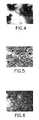
- FIG. 5shows the polishing induced damage in a 2.5 micron GaN epitaxial film grown on the substrate. There is reduced coherent growth and coalescence decorating what appears to be polishing damage or scratches.
- FIG. 7shows the normal morphology of a GaN PIN/10 ⁇ m GaN epi on FS GaN
- FIG. 8shows the morphology degradation of an area where backside evaporative has inhibited the epitaxial layer growth. It is to be noted, however, that the backside evaporative product does not necessarily need to reach the epi surface in order to degrade the morphology, since the degradation product trapped between the susceptor and substrate material may modify the nature and extent of thermal contact, thereby introducing changes that may degrade the morphological uniformity of temperature-sensitive epitaxial layers and device structures.
- the backside decompositionalso changes the surface chemistry and therefore the nature of the electrical contacts formed on the backside of the gallium nitride substrate.
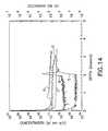
- GaN epi FWHMGaN epi FWHM with increasing x-ray slit size
- the DCXRD FWHM of the substratesincreases with increasing x-ray slit width but at a lower rate than the 10 ⁇ m epitaxial layer and device structure thereon. This increased FWHM at larger slit width is attributed to bowing due to backside substrate evaporation, a thermal stress-related issue, epi tilt, and crystalline domains in the substrate. At smaller slit width the “as grown” FS GaN substrate and epitaxial layer have similar DCXRD FWHM.
- the substrate preparation, interface preparation upon heat-up and substrate cleaning,also create issues in MOVPE GaN growth on FS GaN substrates.
- General reactor conditionsmay also affect epitaxial morphology for growth on FS GaN, resulting in poor interrupted morphologies.
- Proper coating on the susceptor and cleaning of the reactor partsare necessary to reduce contamination at the substrate epi interface.
- the cleanliness of the epitaxial growth systemis less of an issue due to the highly defective interlayers that conventionally are grown on such substrates to reduce the lattice mis-match and strain between epi layer and substrate.
- Contamination at the homoepitaxial interfaceis defined here as any unintentional impurity defect or other flaw within 1000 Angstroms of the homoepitaxial epi and substrate interface and which has a concentration two times greater than the substrate or epi layer at a distance greater than 1000 Angstroms from the interface.
- UV LEDsultraviolet light emitting diodes
- HEMTshigh electron mobility transistors
- LDslaser diodes
- PIN photovoltaic detectorsPIN photovoltaic detectors
- the present inventionrelates to III-V nitride homoepitaxial materials of superior low defect density and surface texture characteristics, and to methods of making the same.
- the term “homoepitaxial” in reference to a material, structure or devicemeans that in such material, structure or device an (Al,In,Ga)N layer is deposited on an (Al,In,Ga)N substrate. Accordingly, consistent with the broad definition of (Al,In,Ga)N, such homoepitaxial material, structure or device can comprise an AlN layer on a GaN substrate, an InN on aAl x Ga 1 ⁇ x N (where 0 ⁇ x ⁇ 1) substrate, an Al x In y Ga 1 ⁇ x ⁇ y N (where 0 ⁇ x ⁇ 1 and 0 ⁇ y ⁇ 1) layer on an InN substrate, etc. Thus, such homoepitaxial material, structure or device is homoepitaxial with respect to the (Al,In,Ga)N group of individual compounds.
- III-V Nitriderefers to a Group III-V compound semiconductor material including nitrogen.
- unfinished substratemeans an (Al,In,Ga)N material as grown by seed or nucleation process, and optionally subdivided (e.g., by fracture cleavage, wire saw cutting into wafer form or the like) and/or subjected (in bulk or subdivided form) to cleaning not involving removal of (Al,In,Ga)N in the cleaning process.
- the term “finished substrate”means an unfinished substrate that has been subjected to further processing (in bulk or subdivided form) involving removal of (Al,In,Ga)N, e.g., by lapping, diamond polishing, etching, chemical mechanical polishing, surface morphological modification, surface defect modification, ion sputtering, surface aberration reduction or removal, pit-filling, mechanical abrading, or the like.
- low pressurein reference to a deposition process means a pressure in the process environment of from about 50 to about 500 torr.
- Low pressure heat-up conditionshave preferred nitrogen partial pressures in the range of from about 1 torr to about 500 torr, and more preferably from about 10 to about 400 torr.
- atmospheric pressurein reference to a deposition process means a pressure in the process environment of from about 500 to about 1000 torr.
- Low pressure and atmospheric pressure deposition processes for (Al,In,Ga)N depositiontypically differ only in the nitrogen partial pressure in the process environment.
- “Atmospheric pressure heat-up conditions”have preferred nitrogen partial pressures in the range of from about 1 torr to about 1000 torr, and more preferably from about 100 to about 800 torr.
- high pressurein reference to a deposition process means a pressure in the process environment above about 1000 torr.
- GaN substrates and GaN epias generally representative for (Al,Ga,In)N substrates and (Al,In,Ga)N epi, respectively.
- deposition processing conditions for homoepitaxial deposition of epi on a substrateare discussed herein primarily in reference to metalorganic vapor phase epitaxy (MOVPE) processes, but the invention broadly contemplates other methods for the formation of epitaxial films of (Al,In,Ga)N on a substrate, including other forms of vapor phase epitaxy such as hydride vapor phase epitaxy (HVPE), molecular beam epitaxy (MBE), sputtering deposition processes, etc.
- MOVPEmetalorganic vapor phase epitaxy
- HVPEhydride vapor phase epitaxy
- MBEmolecular beam epitaxy
- sputtering deposition processesetc.
- the inventionrelates to a method of forming a III-V nitride homoepitaxial layer on a corresponding III-V nitride material substrate with quality comparable to that described in our earlier copending U.S. patent application Ser. No. 09/524,062 filed on Mar. 13, 2000 in the names of Robert P. Vaudo, et al. for “III-V Nitride Substrate Boule and Method of Making and Using the Same,” the disclosure of which hereby is incorporated herein by reference in its entirety.
- the III-V nitride homoepitaxial layeris deposited by a VPE process using Group III source material and nitrogen source material under process conditions including V/III ratio (Group V flux/Group III flux) in a range of from about 1 to about 10 5 , nitrogen source material partial pressure in a range of from about 1 to about 10 3 torr, growth temperature in a range of from about 900 to about 1250 degrees Celsius for GaN, growth temperature in a range of from about 500 to about 1000 degrees Celsius for InGaN, growth temperature in a range of from about 1100 to about 1250 degrees Celsius for AlGaN, growth temperature in a range of from about 600 to about 1250 degrees Celsius for AlInGaN, and growth rate in a range of from about 0.1 to about 500 microns per hour.
- V/III ratioGroup V flux/Group III flux
- the inventionrelates to an epitaxial layer that replicates or improves the material quality of the III-V nitride substrate producing a dislocation density of less than 5E8 dislocations per square centimeter and a DCXRD FWHM of less than 200 arcsecs.
- the inventionrelates to an epitaxial layer on III-V nitride substrate system which has a sheet resistance of greater than 10 4 ohms per square centimeter at room temperature or more preferred greater than 10 5 ohms per square centimeter, and to a method of making the same.
- the inventionrelates to an epitaxial layer and growth sequence that reduces morphology and defect disparities in unfinished or finished FS GaN and a method of making the same.
- the inventionin another aspect, relates to a method of forming a III-V nitride homoepitaxial layer on a corresponding III-V nitride material substrate, comprising depositing the III-V nitride homoepitaxial layer by a VPE process using Group III source material and nitrogen source material, wherein the substrate is reposed on a susceptor surface during such depositing step.
- Such methodin one embodiment further comprises coating the susceptor surface with a corresponding III-V nitride material prior to reposing the substrate thereon for the depositing step, and/or preparing the susceptor and reactor parts with a less volatile and inert coating such as metal carbide (TaC, NbC, etc.).
- a further aspect of the inventionrelates to III-V nitride homoepitaxial materials and structures variously made by the above-described methods.
- the inventionrelates to a III-V nitride homoepitaxial microelectronic device structure comprising a III-V nitride homoepitaxial epi layer on a FS III-V nitride material substrate.
- Additional aspects of the inventionrelate include, without limitation: tilt reduction between crystal grains propagated from the substrate; cleaning of wafers to remove impurities; heat-up conditions on substrates that enhance epi material quality; growth conditions on various orientations that yield preferred epi layers; epi in general on alternative crystallographic planes other than c-planes; protecting the backside of the substrate from evaporation to prevent epitaxial interruption; interlayers between substrate and epi; strain relief layers; pauses in dopant flow in nucleation and nucleating schemes; methods of smoothing; finishing and growth on finished FS GaN; surfactant addition to change growth mechanisms; and methods to facilitate smoothing of unfinished and finished FS GaN.
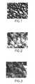
- FIG. 1is a photomicrograph of a FS GaN wafer at 130 ⁇ magnification.
- FIG. 2shows a 2.5 micron GaN MOVPE film formed on a piece of the FS GaN substrate of FIG. 1, at a magnification of 130 ⁇ .
- FIG. 3shows a 7.5 micron GaN MOVPE film on a piece of the FS GaN substrate of FIG. 1, at a magnification of 130 ⁇ .
- FIG. 4is a micrograph at 65 ⁇ magnification, showing a polished FS GaN substrate.
- FIG. 5at a magnification of 65 ⁇ , shows the effect of polishing induced damage in a 2.5 micron thick GaN epitaxial film grown on the substrate of FIG. 4 .
- FIG. 6is an enlarged view, at a magnification of 255 ⁇ , of the GaN film of FIG. 5 .
- FIG. 7is a micrograph, at a magnification of 65 ⁇ , of a GaN PIN/10 microns GaN epi on FS GaN, showing morphology.
- FIG. 8is a micrograph at a magnification of 65 ⁇ , of an area on the growth surface of epi layer in FIG. 7 where backside evaporative product reached the epi.
- FIG. 9is a graph of DCXRD FWHM as a function of increasing slit width for unfinished HVPE GaN substrates and 10 micron epi layer plus device structure thereon.
- FIG. 11shows a typical set of epitaxial growth process steps, wherein the vertical axis loosely denotes temperature and the horizontal axis loosely denotes time.
- FIG. 12is a photomicrograph at 65 ⁇ of a rougher, finely pitted epitaxial morphology obtained with an old GaN substrate cleaning method.
- FIG. 13is a photomicrograph at 65 ⁇ showing a smoother epitaxial morphology obtained with a new GaN substrate cleaning method in accordance with one aspect of the invention.
- FIG. 15is a micrograph of an epilayer on 10 micron HVPE GaN/sapphire showing fish-scale and rough surface morphologies deriving from the growth conditions employed in the film formation.
- FIG. 16shows an AFM scan of a 10 micron GaN epitaxial layer grown on unfinished FS GaN demonstrating well defined step structure, low dislocation density and parallel steps.
- FIG. 17is a DCXRD spectrum of GaN PIN on 10 micron GaN epi on unfinished FS GaN.
- FIG. 18is a micrograph of unfinished FS GaN substrate at 130 ⁇ magnification.
- FIG. 19is a micrograph of 10 micron GaN epitaxial MOVPE layer on unfinished FS GaN, at 130 ⁇ magnification.
- FIG. 20is an atomic force microscope (AFM) micrograph of epitaxial growth on a hex hillock, in a 2 micron ⁇ 2 micron view.
- AFMatomic force microscope
- FIG. 21is an atomic force microscope (AFM) micrograph of epitaxial growth on a hex hillock, in a 10 micron ⁇ 10 micron view.
- AFMatomic force microscope
- FIG. 22is an atomic force microscope (AFM) micrograph of epitaxial growth on a hex hillock, in a 20 micron ⁇ 20 micron view.
- AFMatomic force microscope
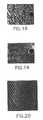
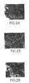
- FIG. 23shows a micrograph at 130 ⁇ magnification of a typical unfinished FS GaN substrate morphology.
- FIG. 28is a micrograph at 130 ⁇ magnification of an unfinished FS GaN morphology.
- FIG. 29is a micrograph at 130 ⁇ magnification of a 10 micron GaN epi on substrate from FIG. 28, showing pit filling
- FIG. 30is a micrograph of the morphology of a target 10 micron GaN epi growth on FS GaN, showing morphology smoothing.
- FIG. 31is a micrograph of the morphology of a target 10 micron GaN epi growth on 10 micron HVPE GaN/sapphire base layer.
- FIG. 32shows a two-step process embodiment of a multi-step process for smoothing an FS GaN unfinished surface.
- FIG. 33is a schematic view of a substrate with epi being grown thereon, illustrating the transport of backside product and interruption of the epi surface morphology.
- FIG. 34shows the morphology of an LED structure on a 10 micron HVPE GaN/Sapphire base layer with a 1000 Angstrom thick undoped GaN nucleation layer.
- FIG. 35shows a corresponding LED structure on a 10 micron HVPE GaN/Sapphire base layer without such an undoped nucleation layer.
- FIG. 36schematically shows a GaN substrate heated to mass transport conditions in an ambient atmosphere of NH 3 and H 2 .
- FIG. 37shows the substrate as mass transport begins smoothing in the ambient.
- FIG. 38shows the substrate at the point that mass transport has smoothed the entire surface.
- FIG. 39shows the substrate with defects including dislocation defect (A), dislocation plus inverted hex pit (B), and inverted hex pit (C).
- FIG. 40shows the substrate with a mask applied to the defect regions.
- FIG. 41shows the substrate with lateral overgrowth of the masked defects.
- FIG. 42in simplified elevation view schematically depicts an FS GaN substrate, showing the surface conformation thereof.
- FIG. 43shows the mesa etched FS GaN substrate surface, with a mesa upwardly extending from the main etched substrate surface.
- FIG. 44shows epitaxial growth on the mesa to produce enhanced smoothing of the epi surface.
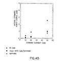
- FIG. 45is a graph of average estimated power output, in milliwatts (three devices) as a function of forward current, in milliamps, of InGaN double heterostructure(DH) LED devices on various substrates.
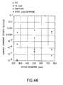
- FIG. 46is a graph of best reverse leakage current density at ⁇ 10V, as a function of device diameter, in micrometers, for 0.25 micron I-thickness PINs on FS GaN, SiC and HVPE GaN/sapphire.
- FSfree-standing in reference to a substrate of (Al,In,Ga)N or other III-V nitride material means that such substrate is a self-supporting structure, e.g., of wafer or plate form.
- the identification of proper growth conditions or growth condition parametersenables growth of high quality epitaxy and the fabrication of high performance devices on FS GaN.
- the growth condition parametersoverlap the ranges used for growth on other substrates, but the optimal conditions for growth differ from those used to grow on sapphire or SiC.
- Aqueous acid (HCl, HNO 3 , etc.) and base cleaning (NH 4 OH, KOH, etc.) methods for FS GaN substratesare employed that are different from those used in the cleaning of other homoepitaxial GaN substrates. These different methods derive from the process differences involved in the formation of the GaN substrates, e.g., HVPE GaN based substrates typically will have reactor deposition products, namely NH 4 Cl, on the wafer surface, deposited during wafer unload, which is required to be removed to achieve high quality homo-epitaxial growth. HCl is used to remove elemental GaN from the substrate surface.
- Oxidation of FS finished GaN substrates followed by a strip (KOH, NH 4 OH, HCl, HF, etc.) just prior to growthis employed to achieve impurity reduction or removal of impurities near the epitaxial surface, as to which room temperature cleaning is deficient.
- Defective wafersare identified by defect regions (pits, scratches, subsurface damage) and such defects are removed by oxidation or the wafer is subjected to re-working.
- oxidationis usefully employed to preferentially and/or completely decorate higher surface energy areas.
- the oxidation of the FS GaN surfaceis employed to preferentially oxidize the hillocks on the surface due to their greater surface energy and different crystal facets, so that the oxide is stripped to create a more smooth surface or a reduced aspect ratio of the hex hillocks.
- This techniquemay also be used to eliminate disparities in the surface resulting from device processing, e.g. to remove rough surfaces (grassing) resulting from micro masking in a reactive ion etching (RIE) step. Repeated treatments of oxide and strip may be employed for the best results.
- RIEreactive ion etching
- RIE cleaningto protect fragile wafer.
- RIEin some embodiments is a preferred method of cleaning the FS GaN substrate.
- RIEenables removal of stubborn surface contaminants from finishing or handling, including some embedded finishing media or other contaminant material from processing, in instances where techniques such as aggressive ultrasonic cleaning may cause the wafer to break or fracture due to its fragility.
- Heat-upenables not only the achievement of the growth temperature, but can advantageously facilitate the occurrence of: 1) smoothing of the substrate surface, 2) removal of damage of the substrate surface, 3) removal of contaminants at the epitaxial substrate surface resulting from processing, 4) reduction of defect propagation at the interface (growth over small pits or dislocations), 5) elimination or reduction of new defect formation (such as vacancies, dislocations, inversion domains, etc.) at the interface, 6) reduction of electrically active dislocations (i.e., H passivates certain types of dislocations), and 7) reduction or modification of substrate impurity out-gassing (e.g., from sulfur in the substrate material, oxygen at the backside of the wafer, etc.).
- the arthas not addressed the use of heat-up conditions and techniques to achieve these advantages in growth on GaN to produce homoepitaxial interfaces.
- Coating of susceptor to prevent contamination during heat-upSusceptor-based contamination is suppressed by coating the susceptor with epi deposition before growth on the FS GaN substrate. Morphology is improved as a result. Impurity reduction of the GaN epi-GaN substrate interface is readily verifiable via SIMS techniques and can be employed for process characterization (e.g., at the GaN epi-HVPE GaN interface, O ⁇ 3E18 cm ⁇ 3 , Si ⁇ 3E18 cm ⁇ 3 and S ⁇ 5E16 cm ⁇ 3 concentrations are readily achievable, which enable high quality homo-epitaxial layers).
- Preferred metal carbide coatingsinclude those that are more inert than SiC coating or SiC:N coatings, such as TaC or NbC, to reduce the possibility of contamination during heat-up.
- Heat-up conditionsPreferred heat-up conditions and associated process parameters include nitrogen species (NH 3 , Amines, N 2 , etc.) at partial pressures in the range of from about 1 torr to about 1000 torr, a ramp time of from about 1 minute to about 1000 minutes, temperature ramp rates in the range of from about 10° C. per minute to about 1000° C. per minute, and the use of an ambient including species such as H 2 , N 2 , Ar, He, Ne, and HCl, and mixtures of two or more of the foregoing.
- nitrogen speciesNH 3 , Amines, N 2 , etc.
- a ramp timeof from about 1 minute to about 1000 minutes
- temperature ramp ratesin the range of from about 10° C. per minute to about 1000° C. per minute
- an ambientincluding species such as H 2 , N 2 , Ar, He, Ne, and HCl, and mixtures of two or more of the foregoing.
- particularly preferred heat-up conditions for low pressure deposition and associated process parametersinclude nitrogen species (amines, N 2 , etc) partial pressures in the range of from about 10 torr to about 400 torr, a ramp time in the range of from about 1 minute to about 100 minutes, temperature ramp rates in the range of from about 100° C. per minute to about 400° C. per minute, and the use of an ambient including species such as H 2 , N 2 , Ar, He, Ne, and HCl, and mixtures thereof.
- nitrogen speciesamines, N 2 , etc
- optimal heat-up conditionsare substantially different for high quality homoepitaxial growth on HVPE GaN FS GaN substrates than those used for growth of 10 micron HVPE GaN/sapphire, or GaN on sapphire, or GaN on SiC interlayers. It will also be appreciated that optimal heat-up conditions may be dependent on the starting and desired end point conditions of the FS GaN wafer with epitaxial film thereon.
- Controlled ambient environmentis employed to facilitate impurity removal or removal of defective surface material, and to maintain uniformity of substrate temperature and temperature of the growth template.
- the ambientadvantageously comprises any suitable gas(es), either single component or multicomponent, including by way of example Ar, N 2 , H 2 , HCl, He, Ne, etc. and any combination of two or more species thereof.
- Addition of impurities during heat-upenables the compensation of charge at the interface to allow highly resistive epitaxial layer substrate interfaces.
- high frequency devicescan be grown and fabricated thereon, taking advantage of the compensation for surface defects to overcome charge non-homogeneity at the surface.
- Crystallographic orientationcan affect growth mechanism, morphology, crystalline quality, film stoichiometry, intentional and unintentional impurity incorporation, strain, carrier transport, optical properties, finishing, RIE and other device fabrication characteristics.
- AFM studiesevidence no significant step bunching or other epitaxial flaw in epi on differing crystal orientations or facets of the GaN substrate.
- Off cut directionas for example ⁇ 11 ⁇ overscore (2) ⁇ 0> or ⁇ 10 ⁇ overscore (1) ⁇ 0>, or therebetween, can be employed.
- different offcut directionsare preferred in various embodiments.
- Ga and N face growthDifferent growth polarity faces can be employed to correspondingly vary growth mechanism, morphology, crystalline quality, film stoichiometry, intentional and unintentional impurity incorporation, strain, carrier transport, optical properties, finishing, RIE and other device fabrication effects.
- Epi growth conditionscan be selectively varied to correspondingly change epitaxial quality and surface morphology.
- growing on FS HVPE GaNwill effect a reduction in impurity incorporation compared to other substrate materials such as LiGaO, LiAlO, SiC, sapphire, etc.
- Growth conditionsare readily optimized to smooth the unfinished HVPE GaN surface.
- Growth conditionsincluding V/III, PNH 3 (Partial Pressure of NH 3 ), T (temperature in degrees Celsius), GR (growth rate in microns per hour) of epitaxial material are selected to effect smoothing of bulk hex mound-like textures and filling of inverted-hex pits (higher V/III and reactor pressure).
- V/IIIVariable Pressure of NH 3
- Ttemperature in degrees Celsius
- GRgrowth rate in microns per hour
- growth ratewhich is primarily dependent on gas flows for a given reactor, temperature and pressure.
- Preferred growth conditions rangesinclude V/III ratio from 1 to 100,000, NH 3 partial pressures in the range of from bout 1 torr to about 500 torr, growth temperature in the range of from about 500° C. to about 1250° C. and growth rates from about 0.1 ⁇ m/hr to about 500 ⁇ m/hr. Most preferred growth conditions include V/III ratio from about 10 to about 50,000, NH 3 partial pressures of from about 20 torr to about 400 torr, growth temperature from about 1000° C. to about 1150° C. and growth rates from about 0.5 ⁇ m/hr to about 10 ⁇ m/hr, for low pressure GaN MOVPE.
- Dislocation reduction Modification-manipulation of growth conditionsis usefully applied to effect dislocation reduction.
- Tilt reduction Orientation selection and modification of growth conditionsare readily selectively applied to achieve crystallographic epitaxial tilt reduction between grains or domains in FS GaN substrates.
- Step flow and macro step formation Growth conditionscan be chosen to selectively achieve desired step flow growth, degree of step bunching, etc.
- RIE conditionscan be adjusted to preferentially expose surfaces, and certain surface exposures can be selected as the growth surface. Corresponding adjustment can be made with a wet etch that is surface selective.
- Impurity addition to growthis utilized for enhanced smoothing or to control polytype fixing.
- Various impuritiesn-dopants, p-dopants, etc
- Impuritiescan be added to adjust the electrical properties and alter the surface morphology compared to the undoped (Al,In,Ga)N film.
- Impuritiescan be added to maintain polytype and crystallographic structures during the growth of the epi on the substrate.
- Surfactantscan be added to preferentially grow or smooth certain areas of the substrate surface.
- Multiple stage smoothing processing for FS GaN homo-epitaxial filmsis beneficially employed in specific applications of the invention. For example, a first set of conditions can be utilized to smooth, reduce dislocation density defect generation, reduce tilt, etc., and a second set of conditions then can be usefully employed to form epitaxial layer(s) for electronics or opto-electronic device structure(s).
- RIEreactive ion etching
- Substrate backside evaporative protectionis an issue, as previously described. Interrupted morphology from backside evaporation product results at higher growth temperatures.
- Temperature ranges in instances where substrate backside evaporative protection is neededPreferred temperature for which substrate backside evaporative protection is desired is in the range of from about 900 to about 1200° C., with most preferred temperature being in the range of from about 1000 to about 1200° C., and further preferred temperature being >1050° C. In the case of In containing substrates, the preferred temperature for which substrate backside protection is desired is >500° C.
- compositions that protect backside from evaporationare usefully identified as having appropriate characteristics, e.g., CTE match to the substrate, adherence to the substrate, not out-gassing, having low vapor pressure, having high thermal conductivity, non-melting at growth temperature, optically reflective or optically transparent, electrically conductive, having specific and controlled conductivity type, inertness, having specific directional conductivity (i.e. lateral or vertical), having engineered narrow reflectivity bands, etc.
- Suitable materialse.g., SiN, SiO 2 , (Al,In,Ga)N, Pd, Ti, Si, Ru, Tu, dielectric stack material, Pt, semiconductor oxides, etc., are readily empirically determinable without undue experimentation, with respect to determining CTE, out-gassing, vapor pressure, thermal conductivity, electrical conductivity and other characteristics of specific materials.
- Materials that protect backside and are n or p-type ohmicsinclude materials described in the preceding paragraph, but also can be an ohmic contact to the wafer.
- Materials that offer structural support for thin FS GaN substratesare materials of the types described in the two preceding paragraphs.
- the materialsmay be chosen to offer support (temporarily or non-temporarily) and to be easily removable to facilitate device fabrication (e.g., by laser facet cleaving).
- a first layermay provide ohmic contact to the GaN layer and a second layer may be suitable for establishing electrical contact to the ohmic contact and for wire bonding.
- Modification of surface energy of backside waferinvolves the removal of high surface energy material from the backside, e.g., by finishing, to reduce the potential of the backside material to evaporate. Finishing of the backside of the wafer with a different orientation to prevent backside evaporation is also useful in various embodiments of the invention. Chemically reacting or alloying the backside of the wafer to make it more inert at higher temperature or to reduce the surface energy is another embodiment of such surface energy modification approach. For example, the back side of (Al,In,Ga)N substrate in one embodiment is oxidized. Other processing steps are useful to passivate or modify the surface in a corresponding manner.
- Materials that improve thermal contact between the susceptor and substratemay include those mentioned in preceding paragraph, that function to deform upon heat-up, and fill in gaps between susceptor and substrate, or otherwise react with the environment to fill in gaps between susceptor and substrate. In general, such materials have high thermal conductivity and enable good and uniform thermal contact between substrate and susceptor. Any suitable material may be used for this purpose, including deformable materials that deform to compensate for surface disparities on either or both of the facing surfaces of the substrate and susceptor.
- Reactor design to eliminate backside evaporationThe reactor design can be adapted for this purpose, in a variety of manners. For example, NH 3 can be flowed behind the wafer or the reactor can be designed in a manner effective to purge the interior volume of the reactor to dilute the evaporating product.
- Low temperature (Al,In,Ga)N growth followed by re-crystallizationis usefully employed in various embodiments of the invention to improve smoothing efficiency (hex hillocks and inverted hex pits), and achieve quicker smoothing time (i.e., less growth time and precursor usage).
- Correction of uniform or non-uniform crystalline orientation and polarity defectsrefers to aspects of the invention that achieve reduction in tilt of grains, mosaicity or inversion domain non-uniformity on the substrate.
- Reduction of dislocationsThis refers to aspects of the invention that reduce dislocations more quickly, reduce certain types of dislocations, and improve material quality.
- FSAl,In,Ga)N
- FSAl,In,Ga)N as produced or supplied can have residual strain, different lattice-matched or mismatched character.
- Al,In,Ga)N compoundscan be employed in epitaxial layers to counteract strain propagation into the epitaxial device structure. High temperature anneals can be employed to reduce the strain, as described more fully hereinafter.
- interlayers deposited between the FS (Al, In, Ga)N substrate and the epitaxial layermay be employed to accomplish improvements in epilayer or device characteristics.
- These interlayersmay be graded in homoepitaxial composition, doping and non-homoepitaxial composition (graded with other material such as SiC, BN, etc).
- Superlatticesone or more layers may be employed to achieve, for example, dislocations bending.
- Thickness of filmA film thickness of undoped GaN epi of less than 1500 Angstroms is necessary to eliminate interrupted morphology in the epi growth and allow initial high quality nucleation of GaN on FS GaN substrates. A more preferred GaN undoped epi thickness would be sufficiently low to allow electron or hole transport across the undoped layer. Corresponding considerations apply to other (Al,In,Ga)N materials.
- N-type dopantsSilane, disilane, germane, oxygen, sulfur, etc. are usefully employed for forming corresponding N-type epi films.
- Cp 2 Mgsolid and liquid, wherein Cp is bis-cyclopentadienyl
- diethylberyllium, zinc, Ca, etc.are usefully employed for forming corresponding P-type epi films.
- Mass Transport Method 1This relates to the selection of a particular ambient to smooth out the FS GaN surface using FS GaN material high surface energy regions. NH 3 and H 2 ambients or H 2 ambients are usefully employed for such purpose.
- Mass Transport Method 2Due to impurities in the substrate during mass transport, dilution before or during mass transport can advantageously be used to smooth morphology. Addition of III-V nitride growth precursors can change the way the smoothing occurs and modify mass transfer driving force or mechanism.
- Mass Transport Method 3Methods 1) and 2) can be employed with the use of a surfactant to enable smoothing to be effected more readily.
- Ambientcan be controlled to facilitate one or more of the preceding Methods in series.
- Electrolytic maskThis approach involves selectively depositing mask material, taking advantage of the electrically active nature of dislocations and defects in the substrate, where the mask material preferentially deposits in areas of electrical activity (i.e., dislocations, defects). Additionally, certain crystallographic facets in unfinished FS (Al,In,Ga)N may have differing electrical activity to allow deposit of the mask selectively on preferred FS (Al,In,Ga)N crystal facets or morphologies. A blanket masking-layer deposition followed by selective removal mitigated by the electrically active defects may also be employed.
- Selective oxide in pits or dislocationsThis involves selective or preferential oxidation or a mask in pits or dislocations having different surface energy and reactivity to the environment.
- Sputter and selective removalinvolves sputtering or depositing a mask on the entire wafer, then using chemical mechanical polishing (CMP) or surface etching to leave a mask in pits, dislocations or remaining morphology characteristics (i.e., a trench between hex facets).
- CMPchemical mechanical polishing
- surface etchingto leave a mask in pits, dislocations or remaining morphology characteristics (i.e., a trench between hex facets).
- Homo-epitaxial (GaN on GaN) growthA homogeneous material (III-V nitride on III-V nitride) technique is employed, using a sufficiently large area to accommodate end device structure growth. Edges of the mesa enable crystallographic plane propagation termination as well as dislocation termination.
- Mask vs. un-maskedThe masked area around the mesa is used to prevent growth or the un-masked structure is etched to sufficient depth to allow large boundary layer diffusion time.
- FIG. 11shows a typical set of epitaxial growth process steps, wherein the vertical axis loosely denotes temperature and the horizontal axis loosely denotes time.
- Such process flowinvolves the steps of wafer cleaning, purging of the reactor, heat-up of the substrate, in-situ cleaning of the growth surface, growth of epi on the growth surface, and cool-down. These steps are discussed in detail in the ensuing description.
- DIH 2 ODeionized water
- DIH 2 ODeionized water
- DIH 2 ODeionized water
- This processis optionally modified to include methylene chloride (MeCl 2 ), acetone and isopropyl alcohol (IPA) cleaning prior to the previously described acid/base aqueous treatment.
- MeCl 2methylene chloride
- IPAisopropyl alcohol
- HVPE GaN based substrate materialincluding both freestanding unfinished or finished GaN as well as 10 micron HVPE GaN/sapphire substrates.
- This cleaning processis also usefully employed to clean oxide or other non-GaN products off the epitaxial surface. Further, such cleaning process has utility for cleaning off impurities or surface contaminants on epitaxial planes other than the c-plane which are exposed on the unfinished surface of both FS GaN and 10 micron HVPE GaN/sapphire.
- An epi-ready surface of FS (Al,In,Ga)Nmay be produced by oxidizing the (Al,In,Ga)N substrate in O 2 , air, an air/inert gas mixture, or a wet mixture to create a thin oxide layer, which is subsequently stripped in an alkali solution or etched off in other suitable manner just before growth.
- the purpose of this thin oxide layeris to getter or remove potential impurities from the substrate, and allow the first few mono-layers of the substrate surface to be free of homo-epitaxial layer interrupting impurities (such as C, Si, S or O) and/or other impurities.
- This processreadily enables production of mobile products (CO, CO 2 , SO 2 , O 2 ) for ease of impurity removal at high temperatures.
- Scan be present in residual levels in the HVPE (Al,In,Ga)N substrate, which will inhibit perfect homo-epitaxial growth.
- the sulfurcan be removed from the substrate by formation of SO 2 gas, thereby leaving the substrate surface and leaving behind a thin oxide layer which can be stripped prior to epi growth.
- Oxidizing the surface of the (Al,In,Ga)N substratecan be utilized to enable defect location, as well as quantification, qualification of quality and/or enhancement of shelf-life of the epi wafer, with the surface of the oxide absorbing hydrocarbons and impurities from the environment and then being easily stripped and under-cut by a selective etch prior to growth.
- the oxidation of the FS GaN surfacecan be utilized to preferentially oxidize the hillocks on the surface due to their greater surface energy and different crystal facets that are exposed.
- a smoother surface or reduced aspect ratio of the hex hillocksis achieved, enabling an easier smoothing of the surface morphology.
- any of the aforementioned oxidations to prepare FS (Al,In,Ga)N unfinished or polished surfacealso can be varied or other nitride (dissimilar) compounds can be employed, including, but not limited to, sulfide, arsenide, antimonide, phosphide, and selenide, in order to facilitate selective etching or removal of dissimilar material at the surface.
- RIEis another alternative method to preparing an epitaxial surface from an unfinished substrate or finished substrate.
- RIEcan remove contaminants that are embedded into the substrate surface, such as finishing media and other material having the potential to outgas during heat-up and growth on the substrate.
- RIEis beneficially employed in instances where aggressive cleaning methods such as ultrasonic cleaning may have a tendency to crack or fracture fragile substrates.
- the ambient conditions in the reactorare also important during the time in which the substrate is being heated to growth temperatures.
- This issue involving ambient conditionsis particularly more complicated with GaN substrates, compared to other substrates used for GaN epitaxy such as SiC and sapphire. This is due to the fact that GaN has a high N-vapor pressure at elevated temperatures and is likely to decompose without adequate NH 3 overpressure or appropriate heat-up conditions. This homo-epitaxial interface, between GaN epi and FS GaN substrate, is prone to contamination, decomposition and initiation of new defects or dislocations if the proper growth conditions are not utilized.
- Desirable and ideal heat-up conditionsshould do one or more of the following; 1) smooth the substrate surface, 2) remove damage on the substrate surface, 3) remove contaminants at the substrate surface, 4) reduce defect propagation at the interface and 5) eliminate new defect formation (vacancies, dislocations, inversion domains, etc.) at the interface, 6) reduce electrically active dislocations, 7) reduce substrate impurity out-gassing and 8) incorporate compensating impurities at the interface.
- heat-up conditions of substratesare also critical in reducing contamination of the substrate epi interface and potential conductivity below the epi structure that can lead to poor isolation of devices and poor high frequency device characteristics.
- impurities such as Si, C and Ocan affect the conductivity of the interface and parameters such as temperature, hydride flow and time have an affect on the conductive interface or contaminants.
- Potential conductivity at the homoepitaxial interfaceis also present for FS (Al,In,Ga)N substrates and 10 micron HVPE GaN/sapphire base layers. From time to time impurities are observed at the epitaxial film and HVPE GaN substrate interface.
- Reactor componentsmay be partly responsible for this contamination of the GaN epitaxial growths. Growth conditions may also affect impurity extraction from growth reactor components (for example, NH 3 may corrode certain parts and enable impurity to pass into gas phase and be incorporated into the film).
- FIGS. 14 and 10show how the condition of a susceptor, either coated with GaN products (results in FIG. 14) or uncoated with GaN products (results in FIG. 10) affects the impurities at the surface of the homoepitaxial interface of GaN and HVPE GaN substrate.
- GaN growth on sapphire or SiCis not as sensitive to bare susceptor components and the interface of GaN and sapphire typically has one or more of Si, O and C. This may be due to the interlayer techniques used on these lattice mismatched substrates and the amenability of the interlayer to accommodate impurities and defects and prevent them from affecting the resultant epi layer. (Al,In,Ga)N surfaces may also have a greater affinity or sticking coefficient for these type of impurities or others. It has been discovered that concentrations below those stated above are required to produce high quality homoepitaxial GaN.
- Preferred heat-up conditions for low pressure MOVPE growthinclude the use of nitrogen species (NH 3 , amines, N 2 ) with partial pressures from about 1 torr to about 500 torr, a ramp time of from about 1 minute to about 1000 minutes, temperature ramp rates of from about 10° C. per minute to about 1000° C. per minute, and use of ambient including species such as H 2 , N 2 , Ar, He, Ne, and HCl and mixtures.
- nitrogen speciesNH 3 , amines, N 2
- partial pressuresfrom about 1 torr to about 500 torr
- a ramp timeof from about 1 minute to about 1000 minutes
- temperature ramp ratesof from about 10° C. per minute to about 1000° C. per minute
- ambientincluding species such as H 2 , N 2 , Ar, He, Ne, and HCl and mixtures.
- Most preferred heat-up conditions parametersinclude nitrogen species (NH 3 , and N 2 ), partial pressures from 10 torr to 400 torr, ramp time of 1 minute to 100 minutes, temperature ramp rates of 100 degrees Celsius per minute to 400 degrees Celsius per minute and ambient including one or more of H 2 , N 2 , Ar, He, Ne, and HCl.
- nitrogen speciesNH 3 , and N 2
- partial pressuresfrom 10 torr to 400 torr
- ramp timeof 1 minute to 100 minutes
- temperature ramp rates100 degrees Celsius per minute to 400 degrees Celsius per minute and ambient including one or more of H 2 , N 2 , Ar, He, Ne, and HCl.
- FS GaN heat-up conditionsinclude heat up conditions that suppress the out-gassing of native impurities in FS GaN, such as S and O, that inhibit good homo-epitaxial growth initiation.
- Sulfurhas been found on HVPE GaN/sapphire wafers using Auger spectroscopy and Secondary Ion Mass Spectroscopy (SIMS) when standard heat-up conditions were used to heat the substrate material to growth temperature and then cooled down. It is suspected that this sulfur material derives from the substrates. Similar issues in other lattice-matched substrates have been encountered as in LGO and LAO where Li impurities and substrate decomposition dramatically affect the epitaxial and interface quality. Additionally, sapphire and SiC substrates have potential issues with species such as Si, C and O, when such species contaminate the interface.
- An alternative to coping with these potential impurities at FS GaN and epitaxial GaN interfaces which are electrically active and conductive,is to compensate them with a deep compensating donor or acceptor such as Mg, Be, C, Si, Ge, O, S, Ca, Fe, Ta, V and Ba to generate charge neutrality without affecting the interface quality.
- a deep compensating donor or acceptorsuch as Mg, Be, C, Si, Ge, O, S, Ca, Fe, Ta, V and Ba to generate charge neutrality without affecting the interface quality.
- Heat-up conditionscan affect the way epi nucleates and can modify how dislocations or defects are propagated.
- the epitaxial growth on c-plane on-axis FS GaN substrateshas been found to be superior to growth on alternative substrates such as sapphire, SiC and LEO (lateral epitaxial overgrowth) or ELOG (epitaxial lateral overgrowth) materials.
- alternative substratessuch as sapphire, SiC and LEO (lateral epitaxial overgrowth) or ELOG (epitaxial lateral overgrowth) materials.
- the AFM structure of GaN epi on these alternative substrateshas non-parallel, irregular step structure, with multiple step terminations, but GaN epi on FS GaN, as shown in FIG. 16 shows a well defined step structure, low dislocation density and parallel steps.
- the epitaxial step structure of this waferis superior to that of any other GaN film on any other substrate published to date of which we are aware, due to its improved parallel step structure, reduced step terminations and reduced pits.
- the AFM step structureis irregular or not well-defined and defect sites are clearly visible.
- the x-ray characteristics of the GaN epi on the FS GaNis superior exhibiting (0004) reflection FWHM of 73 arcsecs as shown in the DCXRD spectrum of GaN PIN on FS GaN in FIG. 17 .
- the x-ray characteristics of the GaN epi on the FS GaNis superior exhibiting (004) (this is OK it can be either) reflection FWHM of 73 arcsecs as shown in the DCXRD spectrum of GaN PIN on FS GaN in FIG. 17 .
- Some of the best surface morphologies ever obtained from an epitaxial layer grown on HVPE GaNare shown for the substrate in FIG. 18 (FS GaN substrate unfinished at 130 ⁇ magnification) and in FIG. 19 (10 ⁇ m GaN epitaxial MOVPE layer on unfinished FS GaN in FIG. 18, at 130 ⁇ magnification).
- the surfacesshow the ability of the epitaxial growth process to smooth out the surface.
- the present inventionembodies growth conditions that tend to preferentially smooth out the unfinished FS (Al,In,Ga)N substrate surface and are broadly applicable to smoothing of finished substrate disparities.
- These growth conditions on unfinished FS GaN substrates that tend to smooth out the substrates surfaceare distinct from the growth conditions that give good smooth homoepitaxial growth on 10 micron HVPE GaN/sapphire wafers or SiC wafers.
- the differences between optimal growth conditions on these types of substratessuggest that the growth mechanisms that produce smooth epi on FS GaN substrate are different, at least in part from those of growth on 10 ⁇ m HVPE GaN/sapphire.
- the homoepitaxial thin films achieved in the practice of the invention on FS (Al,In,Ga)Nhave higher mobility and sheet charge than any other substrate due to the uniform nature and low dislocation density of the epilayer.
- Low dislocation densityalso enables higher dopant incorporation (e.g., of Mg) without deep level compensation if the p-GaN compensating complexes are associated with a dislocation or other structural defect.
- higher carrier concentrationscan be achieved (e.g. hole concentrations from Mg) compared to epitaxy produced on sapphire. Since room temperature carrier concentration (e.g. Mg acceptor concentration) is in part limited by solubility (e.g. Mg solubility), higher material quality enables modification, e.g., enhancement of solubility. This is also true of other dopants.
- Possible substrate orientations for epi growth of GaN in the practice of the inventioninclude offcuts from (0001) or (000 ⁇ overscore (1) ⁇ ), where offcut angle magnitude and direction are important, families of on-axis planar faces such as ⁇ 11 ⁇ overscore (2) ⁇ 0 ⁇ and ⁇ 1 ⁇ overscore (2) ⁇ 00 ⁇ , offcuts from these other faces, and the face itself (Ga and N).
- GaAsboth electronic and opto-electronic devices have been shown to exhibit a strong dependence on the substrate (crystal plane and polarity) and the device orientation, and GaN involves similar considerations.
- the most desirable GaN substrate orientation in various embodimentsis application specific: from device-to-device, depending on whether MBE or OMVPE is employed, depending on the material, alloy, conductivity type and structure being grown.
- Step structure of GaN epi films on various c-axis substrates and substrates with regions containing surfaces slightly misoriented from the c-axishave been evaluated via AFM (Atomic Force Microscopy) on four square micron areas.
- the raw AFM datawas compared without taking probe tip effects into account. Due to the 1 nm lateral probe tip displacement (probe tip effect), raw data analysis results in some number of Ga—N bi-layer steps to be missed and an underestimate of the off-cut angle from the c-axis.
- useful datacan be obtained from the raw AFM data without the exact determination of the orientation of GaN crystal with techniques such as LAUE or RHEED.
- GaN epi on “finished” and “unfinished” GaN substrateshas typically parallel and regular steps with fewer step terminations at defects compared to epi on heterogeneous substrates such as SiC and sapphire.
- Epitaxial GaN layers grown on “finished” and “unfinished” GaN substratesare typically mis-oriented from the c-axis by up to several degrees based on a calculation of the step height and terrace width data from AFM scans. Regardless of the mis-orientation, we typically observe regular and parallel steps. GaN epitaxy grown on heterogeneous substrates such as sapphire and SiC typically exhibit irregular steps and typically less of a mis-orientation from the c-axis as determined from AFM scans.
- Step heightsare typically in the range of 1.2 to 12.0 angstroms for GaN epi on “finished” and “unfinished” GaN substrates while GaN epi layers on heterogeneous substrates such as sapphire and SiC typically exhibit 2.5 to 6.0 angstrom step heights. Unfinished GaN substrates typically exhibits a rougher surface and therefore greater local mis-orientation with respect to the c-axis. Epitaxy grown on these larger mis-orientation angle surfaces from the c-axis typically exhibits greater step heights, but still no step bunching (i.e. no steps greater than 5.0 nanometers).
- Terrace widthsare typically in the range of 300 to 2400 angstroms for GaN epi on “finished” and “unfinished” GaN substrates while GaN epi layers on heterogeneous substrates such as sapphire and SiC typically exhibit terrace widths in the range of 700 to 2400 angstroms. Unfinished GaN substrates typically exhibit a rougher surface and therefore local greater mis-orientation with respect to the c-axis. Epitaxy grown on these larger mis-orientation angle surfaces typically exhibit smaller terrace widths.
- vicinal off-cuts from the Ga-faceare typically 0 to 1.5 degrees for GaN epi layers on “finished” and “unfinished” GaN substrates.
- Off-cuts for GaN epi layers on heterogeneous substrates such as SiC and sapphireare typically less than 0.5 degrees off-cut from the c-axis.
- the potential benefits of using offcut directions from ⁇ 0001>may be based, for example, on SiC and GaAs epitaxial growth considerations.
- the offcutcreates surface steps whose ideal height and width are related to the magnitude of the offcut angle and the polytype.
- the surface stepspromote homoepitaxial growth—step flow growth—where the epilayer inherits the stacking sequence of the substrate.
- the direction of the offcutis also important in determining film quality, doping, etching, reactivity and other properties.
- the magnitude of the offcutis also a consideration: for example, in 4H SiC an 8° offcut typically is preferred over a 4° offcut to reduce triangular inclusion defects. Larger offcut magnitudes can correspondingly reduce dislocations in GaN, but there are also isotropy considerations.
- GaN substrate offcuts, orientations or facespermits reduced growth temperatures in various applications, and InGaN can be grown at different temperatures. Step flow growth can be effected and ternary uniformity can be selectively improved or altered.
- the use of different GaN substrate offcuts, orientations or faces in various aspects of the inventionenables: enhanced dislocation annihilation, increased critical thickness, reduction of cracking or avoidance of cracking entirely, alteration of growth rates; growth of different polytypes; use of different growth precursors on offcut GaN substrates; improvement of growth efficiencies; and use of optimally different—or simpler—forming interlayers schemes and interlayers for growth on GaN substrates.
- interlayersIn reference to forming interlayers (use of interlayers), forming interlayers is generally not preferred in the practice of the present invention, but in some embodiments is usefully employed to selectively eliminate certain types of defects and to reduce the smoothing times of the unfinished substrate surface or to eliminate the need for comprehensive polishing steps and is discussed in greater detail hereinafter.
- Increased Mg or p-type doping in generalmay be achieved when alternative orientation, face or offcut GaN substrates are used.
- Si or n-type doping, in general,can also be altered.
- Impuritiessuch as but not limited to oxygen or carbon contamination can be reduced and other incorporation such as H can be effected.
- the use of alternative orientation, face or offcutscan also affect defect formation, including vacancies, dislocations, defect complexes and passivation of dopants. Impurity diffusion can be altered, intentionally or incidentally, and other dopants can be utilized.
- the piezoelectric effectcan be altered when alternative orientation, face or offcut GaN substrates are employed, yielding selectively alterable effects which are usefully exploited for HFETS and other devices.
- Transport propertieslikewise can be altered, especially as they relate to dislocation formation and/or reduced unintentional impurities.
- the optical propertiescan be improved, due to better interfaces or reduced unintentional impurities, or improved crystalline quality or other effects.
- InGaN orderingcan be altered, and alloy segregation can be effected and exploited.
- AlInGaNmay be more readily controlled and effected with a more homogeneous set of process conditions. Smoother facets can be cleaved to improve optical devices on substrates with different offcuts, face or orientations.
- FIGS. 20-22are atomic force microscope (AFM) micrographs of epitaxial growth on a hex hillock, demonstrating vicinal or non-(0001) epitaxial growth with a low incidence of step bunching.
- FIG. 20shows a 2 micron ⁇ 2 micron view
- FIG. 21a 10 micron ⁇ 10 micron view
- FIG. 22a 20 micron ⁇ 20 micron view.
- FIG. 23shows a micrograph at 130 ⁇ magnification of a typical unfinished FS GaN substrate.
- Hex hillocks and inverted pitsare present on the substrate surface and are atypical surface features on other homo-epitaxial growth surfaces in Si, other III-V materials and WBG semiconductors. These hex hillock and inverted pit features do not always appear on all substrates in the same number or size and desirably are minimized or eliminated from the substrate.
- These hex hillock and inverted pit featuresmay be possible to remove via finishing but there are issues with finishing GaN materials due to their hardness and brittleness. It therefore is highly advantageous and novel to produce a high quality smooth homoepitaxial film directly on the unfinished substrate material, thereby reducing the cost of the substrate and improving the availability and applicability of the substrate in lower cost margin applications.
- FIGS. 24-27demonstrate how epitaxial growth conditions affect the smoothing of FS GaN substrate surfaces.
- GaN growth conditionsincluding a 100 torr reactor pressure and 4.4 slm of NH 3 yielded a uniform AFM step structure across the wafer surface as measured by three areas via AFM (with 10-15 steps per 2 micron length of the wafer surface).
- NH 3 flow rate, reactor pressure, growth temperature and growth ratehave been found to affect the smoothing of the FS GaN unfinished surfaces and implicate corresponding results for finished substrates.
- Preferred low pressure growth conditionsranges include V/Ill ratio from 1 to 100,000, NH 3 partial pressures of from about 1 torr to about 500 torr, growth temperature from about 500 degrees Celsius to about 1250 degrees Celsius and growth rates from about 0.1 micron per hour to about 500 microns per hour.
- Most preferred growth conditions for low pressure growthinclude V/III ratio from about 10 to about 50,000, NH 3 partial pressures of from about 20 torr to about 400 torr, growth temperature from about 1000 degrees Celsius to about 1150 degrees Celsius and growth rates of from about 0.5 micron per hour to about 10 microns per hour. For indium containing compounds much different, lower growth temperatures are typically facilitated. In the case of In containing epi layers, the preferred temperature for which preferred growth temperature is >500° C. Atmospheric pressure processes can be discerned without undue experimentation from the preceding discussion of growth conditions.
- Epitaxial growth conditionssuch as reactor pressure and NH 3 flow, may also affect the degree of pit filling on the unfinished FS GaN substrate material.
- the preferred growth conditionsare the same as those described above. With certain growth conditions, higher V/III pits can be filled completely, as shown in FIGS. 28 and 29.
- FIGS. 28 and 29show before and after growth morphology, respectively, using higher NH 3 flow, as advantageously affecting the pit-filling process, and demonstrating that pit-filling is dependent on growth conditions.
- the growth conditions that smooth out HVPE GaN unfinished substratesare different than the growth conditions that are employed to grow smooth epitaxial films on smoother 10 micron HVPE GaN/sapphire layers. This is shown in FIGS. 30 and 31 in which optimum growth conditions for FS GaN smoothing are employed in GaN epi growth on an FS GaN substrate and on a HVPE GaN/sapphire base layer substrate.
- FIGS. 30 and 31present a comparison of preferred smoothing conditions on FS GaN to same conditions on 10 micron HVPE GaN/sapphire base layers, demonstrating that different growth mechanisms and/or smoothing conditions are needed on different substrates. More specifically, these micrographs show that higher NH 3 flow and reactor pressure produce a rougher circular defect morphology on HVPE GaN/sapphire but have a positive effect on FS GaN substrate growth and smooth morphology.
- the growth conditionsincluding but not limited to growth rate, NH 3 flow, reactor pressure, growth temperature, V/III and PNH 3 , have an effect on how and what type of dislocations propagate or initiate in the interface of the epitaxial layer and the substrate.
- Changing growth conditions, V/III, PNH 3 , temperature and growth rate, to facilitate surface smoothing or dislocation reductioncan be usefully employed to modify the step flow growth of the epitaxial layer.
- Tilt of the HVPE GaN crystals or mosaic pattern in relation to one anothercan also be an issue for epitaxial growth of GaN on FS GaN and adjustment of the growth conditions can affect growth on mis-oriented grains.
- the X-ray FWHM of the GaN crystalis a function of the slit size or width of the X-ray beam.
- the FWHM of epi on FS GaNcan have a broader FWHM than the original FS GaN unfinished substrate. This could be due to the epitaxial film or substrate issues, including but not limited to, bow of the wafer during epitaxy growth or crystallographic defects. Modification of growth conditions may be employed to adjust this tilt or relative miss-orientation to one another.
- FIG. 32shows a two-step process embodiment of a multi-step process for smoothing an FS GaN unfinished surface.
- the left-hand panel (FIG. 32A) of FIG. 32shows the GaN substrate in an ambient of NH 3 and H 2 .
- the middle panel (FIG. 32B) of the Figureshows the epi layer as having been formed to smooth the GaN substrate.
- the right-hand panel (FIG. 32C) of the Figureshows the epi layer as having been further grown to propagate the GaN epitaxy for purposes of forming device structures.
- the inventiontherefore contemplates in one embodiment a two-step process on finished or unfinished material, including a first set of process conditions to reduce substrate processing imperfections, and a second set of (normal) processing conditions to grow device structure(s) on the substrate.
- Doping of the epitaxial filmcan also be used to smooth out the surface of the wafer.
- the morphologytends to be smoother and this characteristic can also be used in epitaxy for FS GaN smoothing.
- Etching (RIE, KOH, etc.) pits to better define the growth surface and then growing over themis another way to eliminate the pits. This methodology is useful regardless of the defect or particulate that is the cause of the pit, with appropriate growth conditions being employed to fill the pit.
- Growth conditionssuch as higher temperature, can be employed to force different polytypes of the GaN crystal, thereby offering corresponding advantages in material and device properties.
- Growth conditions on unfinished FS (Al,In,Ga)Ncan be employed to vary the mechanism in which smoothing of FS (Al,In,Ga)N hex mounds occur.
- Two different methodsare usefully applied, one in which the existing crystallographic planes of the hex mounds are propagated at a lower rate than nucleating c-planes in the valleys, and the other in which the existing crystallographic planes of the crystal hex mound propagates through some range of vicinal surface, ending with an on axis or vicinal c-plane surface.
- These approachescan be applied to other crystallographic planes in the (Al,In,Ga)N crystal.
- MOVPEAl,In,Ga
- native (Al,In,Ga)N substratesThe growth of MOVPE (Al,In,Ga)N on native (Al,In,Ga)N substrates is complicated by the fact the backside (e.g., an N-face) of the substrate has a tendency to evaporate.
- This evaporation or decomposition producttends to transport into the reactor ambient, with potential for depositing on the epi surface and causing surface damage or growth ambient transients that impairs epitaxial layer quality.
- the diffusion of this productinterrupts the epi surface morphology as schematically illustrated in FIG. 33, showing the migration of backside evaporative products to the epilayer and interrupting the surface.
- this evaporative productis GaN evaporating off the backside of the FS GaN wafers and escaping into the growth environment due to high elemental vapor pressure of N in GaN at elevated temperatures.
- This evaporative productmixes with the growth environment and transports to the epi surface resulting in epitaxial growth interruption.
- the backside of the GaN substrateis stable in our experimentation to about 1050 degrees Celsius but at temperatures higher than 1050 degrees Celsius the backside (N-face) begins to decompose fairly readily.
- the temperature measured in our apparatusis measured with a thermocouple (Type R/S) positioned outside of the growth ambient but inside a quartz sheath inserted into the susceptor. This temperature measurement technique allows for some error in calculating the exact temperature of the susceptor. We suspect this error to be less than 100 degrees Celsius.
- the preferred growth temperature range for non-backside evaporationis ⁇ 900 degrees Celsius and the preferred growth temperature range for backside protection is ⁇ 900 degrees Celsius.
- the temperature for which backside protection is preferredis >500° C.
- the superior crystalline material quality of the FS GaN substratesenables higher power, short wavelength blue, green and UV lasers and LEDs as well as higher frequency and higher power electronics, and higher temperature growth conditions may be necessary to enable the epitaxial material quality to be of comparable material quality to that of the substrate.
- a preferred approach to eliminating this backside evaporation product issueis to deposit a backside protection layer to the backside of the substrate in contact with the susceptor.
- This layerserves as a substrate temperature stabilization layer and also can function as a support film, a contact metal and/or a backside protection, thermal contact improvement layer, and/or thermal contact uniformity improvement layer, depending on the layer used and the need.
- a backside protection layershould be nominally inert to the growth environment, have a very low vapor pressure at growth temperatures and not contribute to background impurities in the epitaxial film.
- the backside protectionmay also serve as a thermal contact layer to the substrate when the substrate has slight bow or other non-planarity, thereby enabling better epitaxial growth and temperature uniformity across the wafer at higher temperatures.
- the materialmay be optically reflective or transparent for opto-electronics applications.
- the backside protective layercan also serve as an ohmic contact layer for the as-grown device substrate, necessitating only the contacting of the p-layer, n-layer or undoped layer.
- itcan comprise a sputtered film of W or other material on the backside of the wafer.
- Other materials that can be usedinclude noble metals.
- SiO 2 , AlN, or Si 3 N 4may be used.
- the material chosenwill have a coefficient of thermal expansion similar to the (Al,In,Ga)N material that is used. It may prove advantageous to employ a thin “glue” layer, e.g. Ti, to promote adhesion if a less reactive material is employed.
- Pd, Ti or other material or metalscan serve not only as protection but also as a contact layer eliminating post-growth processing steps in the device fabrication, e.g., of multiple layer dielectric stacks that are conductive and have engineered reflectivity at certain wavelengths.
- Multiple materialsmay need to be deposited to the backside of the wafer to provide collective properties deriving from various materials (e.g., one layer to protect substrate evaporation and another layer to protect the substrate evaporation suppression layer and a third layer for bonding).
- the additional backside protection layer or layersmay be removed post-growth to provide the desired epitaxial wafer characteristics.
- Multiple materialscan be deposited to enable improved processing of the device (e.g., one layer is used to improve ohmic contacts to substrate, and a second layer allows contact to the ohmic layer and improved or more robust wire-bonding).
- the finishing of the backside of the wafer to a certain finishis advantageous to reduce the backside evaporation product.
- reducing the defect level of the backsidewill reduce the backside evaporative product. Finishing reduces the surface energy of the backside of the substrate and reduces the potential to evaporate. Additionally, finishing the backside of the wafer to a certain orientation alters backside evaporation products. Modification of the backside surface may also include reaction with another species to enable the backside to be inert to the growth environment.
- Various orientations of GaNmay have a lower susceptibility to decomposition at higher growth temperatures. This permits a resolution of the decomposition issue, by use of different orientation wafers or miscuts for the backside of the wafer.
- the backside evaporation product that is an issue for the backside of a Ga-face substratepreferably is overcome by the above-described methods of backside protection.
- Backside evaporationalso causes the substrate to stick to the susceptor, necessitating the substrate to be pried off the susceptor pocket, with consequent potential for damage to the epi layer and substrate by cracking or scratching.
- the deposit left behind on the susceptoralso has the potential to significantly inhibit the formation of high quality material or the achievement of good uniformity on the next runs done using that susceptor pocket. Additionally, if the substrate adheres too strongly to the susceptor, then damage to the substrate due to TCE differences is a possible occurrence upon cool-down.
- Backside protectioncan also be used to reduce bow in the substrate.
- Some x-ray datasuggest that the breadth of the x-ray peak increases with MOVPE epi, but this occurrence is likely attributable to bow arising from the non-uniform production of the backside evaporative product.
- Materials that are advantageous to reduce bow in the substrateinclude materials that have a different CTE such that cool-down of the composite GaN substrate and backside protection pull the substrate wafer to a flat shape, and/or reduce or improve uniformity of the backside evaporative deposition to allow more uniform strain across the wafer, reducing bow therein.
- the reactor designcan be adapted for the purpose of protecting the backside of the wafer from evaporation, in a variety of manners.
- NH 3 or nitrogeneous speciescan be flowed behind the wafer or the reactor can be designed in a manner effective to purge the interior volume of the reactor to dilute the evaporating product.
- the present inventioncontemplates the fabrication of GaN low T interlayers followed by a re-crystallization step to improve the as-grown surface morphology of the FS GaN.
- This approachenables a superior value-added FS GaN product by reducing growth time in the reactor that is otherwise required to smooth out the epitaxial surface.
- low temperature interlayerscan be used to reduce dislocations and certain types of defects, including inverted hex pits, grain boundaries, and inversion domains.
- the interlayerin some embodiments is used to absorb impurities and/or compensate native defects in the re-crystallized interlayer.
- the inventionalso contemplates use of such interlayers for reducing tilt between domains and crystal grains in the FS GaN films during homoepitaxial growth as well as for reducing mosaicity, reducing inversion domains, and/or placing N-face and Ga-face crystals near one another to generate a uniform polarity epitaxial surface by allowing a high defect reducing affinity layer to absorb dislocations and crystal imperfections.
- the inventionin another aspect contemplates a high temperature anneal step, preferably at a temperature >600° C., prior to growth, or in situ, to relieve the strain in the layer, with the ambient of the anneal being changed to protect the substrate surface and promote substrate strain relaxation. Under some circumstances it may be advantageous to anneal and relieve strain subsequent to epilayer growth but prior to dicing or cleaving the fully fabricated wafer.
- the inventioncontemplates growth on the substrate surface of (Al,In,Ga)N compounds and super-lattices of different lattice constant (Al,In,Ga)N alloys, to counteract the substrate strain and enable strain-free device growth on the substrate.
- Another approach to relieve strain from the substrate and prevent it from propagating into the epitaxial layeris to use a graded transition between alloys of the epi layer and the substrate. Additionally, thin strained layers or superlattices can be employed with layers having less than the critical thickness, to relieve strain in the epitaxial device structure.
- Interlayers between substrate and epitaxial layer or substrate and epitaxial layer plus device structure thereoncan be employed to do one of the following but not limited to strain modification, dislocation reduction and optical reflection.
- the interlayerscan be deposited at low temperature, high temperature, in superlattice configuration (one or more layers), graded in composition, graded in doping level, delta-doped (thin heavily doped layers) and chosen from III-nitrides, SiC, B—N, etc.
- Grading of a homoepitaxial interlayeris defined as grading the composition of Al x In y Ga 1 ⁇ x ⁇ y N between the ranges of 0 ⁇ x ⁇ 1 and 0 ⁇ y ⁇ 1. Grading may occur in a convention of higher to lower parameter from substrate to epitaxy, respectively, or lower to higher parameter from substrate to epitaxy, respectively, where the designation of parameter refers to bandgap, lattice parameter or doping. Grading may occur in a linear, parabolic, exponential or other fashion depending on the structure. Strain introduced through deposition of the interlayer may affect bandgap and/or lattice parameter. Grading can be continuous or comprised of multiple discrete layers. Doping transitions, multiple graded layers and permutations of the above mentioned may be employed.
- Interlayersmay be uniform in composition, bandgap or doping.
- Interlayersmay be utilized in a superlattice configuration to enable specific reflectivity or absorption bands to be engineered, to enable dislocations to bend over and terminate propagation in the growth direction, or for other suitable applications.
- Patterned interlayersmay be utilized for defect reduction, crack reduction, or lateral growth there-from, patterned aspect to patterned aspect.
- the inventionalso contemplates the use of heteroepitaxial techniques in the fabrication of “dissimilar” homoepitaxial articles, where different substrate and epi (Al,In,Ga)N materials are employed.
- the initiation of the dopant species too early during the nucleation of the epitaxial GaN layer growth on the FS GaN substratecan inhibit high quality homoepitaxial growth, by the introduction of high concentrations of Si and Mg or dopant, in general, at the interface, or the formation of other defects.
- FIGS. 34 and 35show a comparison of surface morphologies of LED structures with n-GaN (layers 1E19 cm ⁇ 3 ) with and without an undoped GaN nucleation layer.
- FIG. 34shows an LED structure with a 1000 Angstrom thick undoped GaN nucleation layer.
- FIG. 35shows a corresponding LED structure without such an undoped nucleation layer. Inserting a thin undoped layer of material to allow nucleation and propagation of the substrate thus allows for high quality homoepitaxial growth.
- the inventioncontemplates in such respect a ⁇ 1500 A thick film of undoped GaN to be deposited on the substrate prior to the introduction of any dopant species. With this thickness of undoped film, the vertical electrical transport resistance is minimized and electron or hole transport across the interface can be realized.
- the smoothing of FS GaN morphologyis necessary for high quality homo-epitaxial growth.
- the undesirable surface texture of the unfinished HVPE FS GaN substrateis an issue in high quality homo-epitaxial GaN growth.
- the present inventionin another aspect contemplates the use of mass transport to smooth surface texture of FS GaN films.
- mass transportis advantageous over other methods of substrate smoothing: 1) it uses minimal amounts of precursors compared to MOVPE overgrowth, 2) the time to perform the mass transport can be dramatically reduced by adjusting the transport conditions (low P, ambient and temperature), 3) it eliminates the difficult task of finishing the wafer and the concomitant effect of inflicting damage to the substrate, or eliminates the final finishing steps, 4) it can be performed ex-situ to enable higher reactor throughput, 5) it is a controllable process that can be used to characterize defects in the material prior to epitaxial growth or shipment of the wafers, 6) it enables dislocation annealing and reduction of the substrate material near the epitaxial interface and 7) it enables a reduction or re-distribution of impurities in the substrate material to be achieved, thereby facilitating better epitaxial growth at the interface.
- the substrateis annealed at higher temperature in an overpressure of ammonia or other N-species precursor and some ambient, either H 2 or N 2 .
- Higher surface energy crystallographic featureshex hillocks, pits
- Mass transport conditionscan be modified to control the quality (defect level, conductivity, etc) of the mass transported material.
- FIG. 36the GaN substrate is heated to mass transport conditions in an ambient atmosphere of NH 3 and H 2 .
- FIG. 37shows the substrate as mass transport begins smoothing in the ambient.
- FIG. 38shows the substrate at the point that mass transport has smoothed the entire surface.
- Mass transport conditions and timesare adjustable to facilitate optimized smoothing and rate of smoothing by mass transport. Further, multiple process mass transport can be employed to optimize the mass transport smoothing characteristics of the substrate.
- the present inventioncontemplates in a further embodiment the growth of a thin layer having a thickness of a thousand Angstroms or less, to facilitate the mass transport smoothing by using mass transport with epitaxial quality MOVPE layers, to dilute the impurities from the substrate material and thereby achieve higher quality mass transport.
- TMGtrimethylgallium
- epi layers of certain (Al,In,Ga)N compositionscan also be used to facilitate the preferential smoothing of a certain facet of the substrate unfinished surface.
- This approachtakes advantage of the fact that certain atoms (e.g., Al, Ga and In) have an affinity for certain crystallographic planes, offcuts or faces in GaN, which allows quicker smoothing for subsequent epi.
- Lattice matched mass transport plus epi, as well as superlattice epi mass transportcan be used to facilitate smoothing and defect reduction of the epitaxial substrate surface.
- Mass transport by either Method 1 or Method 2can be enhanced by the addition of a surfactant to smooth out the surface of the epi layer at higher rate.
- a surfactantto smooth out the surface of the epi layer at higher rate.
- Bismuth and other chemicalscan be employed as surfactants to aid the propagation of certain (Al,In,Ga)N crystallographic planes preferentially over others.
- Mass transportis conducted by either Method 1, Method 2 or Method 3, while adding charge compensating impurities which can negate native and other impurities-related charges in the mass transport film which has been deposited.
- Intentional doping or impurity incorporation at the interfacecan be employed to modify electrical properties (charge, conductivity, conductivity type, charge neutrality, etc.).
- Intentional dopant incorporationcan include but are not limited to one or more of the following: Mg, Be, Ca, C, Si, O, Ge, V, Fe, S, Cr, etc.
- One approachis to anneal the surface damage at growth temperature in H 2 or NH 3 , or both.
- a second approach to remove surface damage on the substrateis to etch back the substrate material with the H 2 and NH 3 ambient, to remove substrate material to beneath the region of damage on the substrate.
- the inventionin another aspect contemplates a method to remove the substrate defects in the unfinished or finished substrate material, in particular pits and dislocations defects.
- the methodincludes the step of selectively masking the defective area with SiO 2 , Ga 2 O 3 , SiN or other suitable mask material, to inhibit growth.
- FIG. 39shows the substrate with defects including dislocation defect (A), dislocation plus inverted hex pit (B), and inverted hex pit (C).
- FIG. 40shows the substrate with a mask applied to the defect regions.
- FIG. 41shows the substrate with lateral overgrowth of the masked defects.
- the maskis selectively deposited in the defect, by electrolytic techniques, by sputtering a film, or using other suitable technique, then the mask is removed, e.g., through RIE, or by chemical mechanically polishing (CMPing) the substrate to reveal the masked defects, or by thermal oxidation to oxidize the substrate followed by stripping of the oxide from the wafer by CMP or other method like RIE (with the assumption that the oxide around the defect grows thicker than the oxide on the planar surface and will fill in the defect to allow overgrowth easily).
- RIEreactive etching
- Electrolytic techniquescan be used if the defects have a different electrical activity than the bulk of the material. Blanket masking followed by selective stripping of the mask material around the defects is more difficult to accomplish, and is accordingly less preferred.
- the inventioncontemplates addition of surfactant into the growth ambient of the reactor during epitaxial growth to facilitate and enhance the smoothing of HVPE GaN unfinished or finished materials.
- the surfactantenables preferential growth on certain crystallographic facets and inhibits growth on others.
- the surfactantcan also be utilized to aid in polytype fixing.
- Growth conditionscan be optimized or multiple process steps can be used to tailor the smoothing of the unfinished or finished substrate surface.
- Illustrative surfactantsinclude indium, due to its high elemental vapor pressure at elevated temperature, and bismuth, since it does not incorporate in GaN at high concentrations.
- Preferred surfactantsmodify the growth mechanism of crystallographic propagation for selective propagation of crystal orientations, thereby smoothing growth, but do not incorporate appreciably into the growing epitaxial layer.
- the inventionin another aspect contemplates etching of mesas on the FS GaN substrate to enable quicker smoothing growth of FS GaN substrate surface.
- This approachallows dislocations, planes and facets to propagate to the mesa edge, to achieve termination and annihilation of defects and crystallographic planes at the mesa edge.
- the general processis illustrated with reference to FIGS. 42-44.
- This mesa etching techniqueinvolves a homoepitaxial or homogeneous material (III-V nitride) technique that forms a smaller or larger mesa geometry than the final device structure and the mesa is made larger or smaller by growth to accommodate the final device structure.
- III-V nitrideIII-V nitride
- a growth-inhibiting maskis placed on the mesa-etched area to prevent growth from occurring. This technique enables reduced strain fields from the substrate into the epi and enables higher mismatch compositions to occur without relaxation, as well as thicker structures to be realized, e.g., VCSELs and other device structures.
- epitaxy and epitaxy plus device structuremay be deposited on posts or mesas in the substrate surface which have been preferentially defined in the substrate surface by etching, mechanical removal, and other means. Epitaxy on these post can be performed to effect reduced dislocation and crack reduction as well as other advantageous effects. Growth conditions can be modified to reduce the dislocation of the epitaxial material on the posts or mesas as well as create a uniform surface level by lateral over growth.
- the trenchesmay or may not be inhibited from nucleation of growth of epitaxial material there-in by one following but not limited to; masking, orientation modifications, native materials which have been made dissimilar, oxides, mechanical damage to change surface energy, etc.
- Mesa or post geometriescan be modified to various fundamental and combinations of fundamental shapes such as circles, squares, rectangles (stripes) and may be oriented on the substrate surface is certain preferred orientation in plane to generate desired affect.
- the desired resistivity of such materialis lower than 1.0 ohm-cm, more preferably lower than 0.4 ohm-cm, and most preferably less than 0.1 ohm-cm.
- GaN material in accordance with one specific aspect of the inventionhas less than 1E8 cm ⁇ 2 and preferably less than 1E7 cm ⁇ 2 dislocation density. Low dislocation density enables higher (dopant) Mg incorporation.
- a p-type GaN film of preferred characterhas >1E19 cm ⁇ 3 Mg, with a dislocation density of less than 1E7 cm ⁇ 2 and more preferably less than 5E6 cm ⁇ 2 .
- Another preferred p-type GaN filmhas >5E19 cm ⁇ 3 Mg with a dislocation density less than 5E7 cm ⁇ 2 and more preferably less than 1E7 cm ⁇ 2 .
- a still further preferred p-type GaN filmhas >1E20 cm ⁇ 3 Mg with a dislocation density less than 5E8 cm ⁇ 2 and more preferably less than 1E8 cm ⁇ 2 .
- Another smoothing method or mechanismeffects propagation of the hexagonal facets through a range of vicinal surface off of the original surface plane (and potentially other planes and vicinal cuts) and smoothing the surface in a truncated manner.
- a still further smoothing methodutilizes the creation of new c-planes in the smoothing process.
- a particularly preferred homoepitaxial layer in the broad practice of the inventionis one which has been grown above its pseudomorphic thickness and generates ⁇ 100 times more dislocations in the epitaxial layer, with a most preferred material having less than one order of magnitude of dislocations in epitaxial layer, e.g., an epi layer with less than 1E8 cm ⁇ 2 and more preferably an epi layer less than 1E7 cm ⁇ 2 .
- a substrateis cleaned, then loaded onto a susceptor inside a reactor vessel.
- the reactor vesselis purged with inert gas until the reactor ambient has been purged of air.
- the process gas ambientis changed to the growth ambient, which protects the GaN substrate material during heat-up.
- the substrateis heated to growth temperature. Once the temperature for growth is reached, typically around 1100 degrees Celsius a cleaning process is completed in the reactor ambient to clean the substrate surface.
- precursorsincluding, but not limited to, TMG, TMA, TMI, GaCl 3 , NH 3 , amines, etc., are introduced into the reactor and decompose on the substrate surface to form the epitaxial thin film material.
- the precursors and ambientare modified during the growth period to enable structures comprising different layers of AlInGaN of p, n or undoped conductivity type to form device structures.
- the precursorsare turned off and the reactor begins to cool. Process gases are used during cooling to prevent damage to the epitaxial layer. Once the wafer is cooled the reactor is purged with an inert gas and then the wafer is unloaded and subjected to the next desired process (device fabrication, characterization, etc.).
- High quality homo-epitaxial epi layers on GaN substratesmay be verified by one or more of the following: optical photo-pumping measurements, atomic force microscopy, positron analysis, transmission electron microscopy, x-ray analysis, secondary ion mass spectroscopy, as well as by other techniques.
- a CTE match of susceptor and susceptor coatingwill enable longer lifetime of susceptor to be achieved, as well as eliminate potential for cracking of the susceptor coating and leaching of impurities from the susceptor core (e.g. graphite).
- the sensitivity of the epi process to the susceptor components in practice of the process of the inventionis surprising, because GaN growth on other surfaces such as AlN, sapphire and SiC are not sensitive to bare susceptor components.
- Controlled reactor flow and ambientmay be necessary in some instances to achieve substrate temperature and substrate temperature uniformity due to cooling effects of the substrate.
- GaN epi on FS GaNdemonstrates well-defined step structure, having a well-defined, parallel and uniform step width without indication of step bunching.
- Step densityis a function of crystal orientation.
- Devices grown on conventional substrateswork well, but do not yet perform at the level desired by end-users due to substrate material compatibility and quality issues.
- High material quality, low dislocation density, lattice-match and CTE matchis extremely important for many devices currently being developed or commercialized in the GaN field such as lasers, UV LEDs, AlGaN/GaN high electron mobility transistors (HEMTs), etc.
- HEMTshigh electron mobility transistors
- UV LEDs on FS GaNexhibited a four-to-five fold improvement in output power characteristics compared to devices on alternative substrates as demonstrated in FIG. 45 .
- UV LEDsare known to improve with increasing material quality.
- UV LEDs on ELOG or LEO GaNdemonstrate an improvement of 20% compared to growth directly on sapphire.
- Growth on FS GaN in accordance with the present inventionwas found to increase LED output power by a factor of four to five times compared to same device structure on sapphire. This is a substantially greater level of improvement than the ELOG layer in which the device traverses several low and high dislocation areas, a fact indicative of the vastly superior quality of devices in accordance with the present invention.
- FS GaNhas a more uniform dislocation density across the entire area of the device and a substantially lower average number of dislocations in the device.
- FIG. 46is a graph of best reverse leakage current density at ⁇ 10V, as a function of device diameter, in micrometers, for 0.25 micron I-thickness PINs on FS GaN, SiC, sapphire and HVPE GaN/sapphire.
- substrate orientationaffects various crystallographic substrate orientations for epi growth.
- substrate orientationincludes the following: growth mechanism; morphology (mis-orientation to ⁇ 11 ⁇ overscore (2) ⁇ 0> on the N-face of the GaN substrate from zero to four degrees reduced hillock formation); crystalline quality; film stoichiometry; intentional and unintentional impurity incorporation; strain; carrier transport (hole-mass has been calculated to be lighter in non (0001) planes, which can have dramatic impact on the p-type doping of GaN; in addition, orientation affects piezoelectric field and strain affects transport properties); optical properties (non-0001 orientation is calculated to have higher optical gain and GaN/AlGaN structures with ⁇ 1 ⁇ overscore (1) ⁇ 00 ⁇ orientation have applicability to lower threshold current densities in lasers; piezoelectric field affects strain and optical interband absorption properties and is dependent on orientation); polishing;
- FS GaNOne significant advantage of FS GaN is fabricating without the requirement of interlayer structures, but in some applications, for example, for morphology smoothing and elimination of defects, interlayers may be advantageous.
Landscapes
- Engineering & Computer Science (AREA)
- Chemical & Material Sciences (AREA)
- Manufacturing & Machinery (AREA)
- Power Engineering (AREA)
- Microelectronics & Electronic Packaging (AREA)
- Computer Hardware Design (AREA)
- Physics & Mathematics (AREA)
- Condensed Matter Physics & Semiconductors (AREA)
- General Physics & Mathematics (AREA)
- Crystallography & Structural Chemistry (AREA)
- Materials Engineering (AREA)
- Organic Chemistry (AREA)
- Metallurgy (AREA)
- General Chemical & Material Sciences (AREA)
- Chemical Kinetics & Catalysis (AREA)
- Inorganic Chemistry (AREA)
- Crystals, And After-Treatments Of Crystals (AREA)
- Chemical Vapour Deposition (AREA)
- Junction Field-Effect Transistors (AREA)
- Semiconductor Lasers (AREA)
- Led Devices (AREA)
Abstract
Description
Claims (73)
Priority Applications (12)
| Application Number | Priority Date | Filing Date | Title |
|---|---|---|---|
| US09/605,195US6447604B1 (en) | 2000-03-13 | 2000-06-28 | Method for achieving improved epitaxy quality (surface texture and defect density) on free-standing (aluminum, indium, gallium) nitride ((al,in,ga)n) substrates for opto-electronic and electronic devices |
| KR1020077019660AKR100856447B1 (en) | 2000-06-28 | 2001-06-27 | How to improve epitaxy quality (surface texture and defect density) on freestanding (aluminum, indium, gallium) nitride substrates for optoelectronic and electronic devices |
| KR1020027017929AKR100810554B1 (en) | 2000-06-28 | 2001-06-27 | How to improve epitaxy quality (surface texture and defect density) on freestanding (aluminum, indium, gallium) nitride substrates for optoelectronic and electronic devices |
| JP2002505658AJP5361107B2 (en) | 2000-06-28 | 2001-06-27 | Method for improving the epitaxy quality (surface roughness and defect density) of aluminum nitride, indium, gallium ((Al, In, Ga) N) free-standing substrates for optoelectronic devices and electronics devices |
| EP10011037.8AEP2290136B1 (en) | 2000-06-28 | 2001-06-27 | Method for achieving improved epitaxy quality (surface texture and defect densitity) on free-standing (aluminum, indium, gallium) nitride ((Al, In, Ga)N) substrates for opto-electronic and electronic devices |
| EP01946718AEP1299900B1 (en) | 2000-06-28 | 2001-06-27 | METHOD FOR ACHIEVING IMPROVED EPITAXY QUALITY (SURFACE TEXTURE AND DEFECT DENSITY) ON FREE-STANDING (ALUMINUM, INDIUM, GALLIUM) NITRIDE ((Al,In,Ga)N) SUBSTRATES FOR OPTO-ELECTRONIC AND ELECTRONIC DEVICES |
| EP10011760AEP2284297B1 (en) | 2000-06-28 | 2001-06-27 | Method for achieving improved epitaxy quality (surface texture and defect density) on free-standing (aluminium, indium, gallium) nitride ((AI, In,Ga)N) substrates for opto-electronic and electronic devices |
| EP10011036.0AEP2290135B1 (en) | 2000-06-28 | 2001-06-27 | Method for achieving improved epitaxy quality (surface texture and defect densitity) on free-standing (aluminum, indium, gallium) nitride ((Al, In, Ga)N) substrates for opto-electronic and electronic devices |
| AU2001268730AAU2001268730A1 (en) | 2000-06-28 | 2001-06-27 | Method for achieving improved epitaxy quality (surface texture and defect density) on free-standing (aluminum, indium, gallium) nitride ((al,in,ga)n) substratesfor opto-electronic and electronic devices |
| PCT/US2001/020409WO2002001608A2 (en) | 2000-06-28 | 2001-06-27 | METHOD FOR ACHIEVING IMPROVED EPITAXY QUALITY (SURFACE TEXTURE AND DEFECT DENSITY) ON FREE-STANDING (ALUMINUM, INDIUM, GALLIUM) NITRIDE ((Al,In,Ga)N) SUBSTRATES FOR OPTO-ELECTRONIC AND ELECTRONIC DEVICES |
| TW090115729ATW516102B (en) | 2000-06-28 | 2001-06-28 | Method for achieving improved epitaxy quality (surface texture and defect density) on free-standing (aluminum, indium, gallium) nitride ((Al, In, Ga)N)substrates for opto-electronic and electronic devices |
| JP2011183170AJP2011251905A (en) | 2000-06-28 | 2011-08-24 | Homoepitaxial iii-v nitride article, device, and method of forming iii-v nitride homoepitaxial layer |
Applications Claiming Priority (2)
| Application Number | Priority Date | Filing Date | Title |
|---|---|---|---|
| US09/524,062US6596079B1 (en) | 2000-03-13 | 2000-03-13 | III-V nitride substrate boule and method of making and using the same |
| US09/605,195US6447604B1 (en) | 2000-03-13 | 2000-06-28 | Method for achieving improved epitaxy quality (surface texture and defect density) on free-standing (aluminum, indium, gallium) nitride ((al,in,ga)n) substrates for opto-electronic and electronic devices |
Related Parent Applications (1)
| Application Number | Title | Priority Date | Filing Date |
|---|---|---|---|
| US09/524,062Continuation-In-PartUS6596079B1 (en) | 2000-03-13 | 2000-03-13 | III-V nitride substrate boule and method of making and using the same |
Publications (1)
| Publication Number | Publication Date |
|---|---|
| US6447604B1true US6447604B1 (en) | 2002-09-10 |
Family
ID=24422619
Family Applications (1)
| Application Number | Title | Priority Date | Filing Date |
|---|---|---|---|
| US09/605,195Expired - LifetimeUS6447604B1 (en) | 2000-03-13 | 2000-06-28 | Method for achieving improved epitaxy quality (surface texture and defect density) on free-standing (aluminum, indium, gallium) nitride ((al,in,ga)n) substrates for opto-electronic and electronic devices |
Country Status (7)
| Country | Link |
|---|---|
| US (1) | US6447604B1 (en) |
| EP (4) | EP2290135B1 (en) |
| JP (2) | JP5361107B2 (en) |
| KR (2) | KR100810554B1 (en) |
| AU (1) | AU2001268730A1 (en) |
| TW (1) | TW516102B (en) |
| WO (1) | WO2002001608A2 (en) |
Cited By (119)
| Publication number | Priority date | Publication date | Assignee | Title |
|---|---|---|---|---|
| US20020043331A1 (en)* | 2000-08-25 | 2002-04-18 | Toyoda Gosei Co., Ltd. | Method for manufacturing a group III nitride compound semiconductor device |
| US20020068201A1 (en)* | 1994-01-27 | 2002-06-06 | Vaudo Robert P. | Free-standing (Al, Ga, In)N and parting method for forming same |
| US20020155713A1 (en)* | 2001-03-30 | 2002-10-24 | Technologies & Devices International, Inc. | Apparatus for epitaxially growing semiconductor device structures with sharp layer interfaces utilizing HVPE |
| US20020189531A1 (en)* | 2001-06-06 | 2002-12-19 | Dwilinski Robert Tomasz | Process and apparatus for obtaining bulk monocrystalline gallium-containing nitride |
| US6613461B1 (en)* | 1999-09-30 | 2003-09-02 | Sharp Kabushiki Kaisha | Gallium nitride-based compound semiconductor chip and method for producing the same, and gallium nitride-based compound semiconductor wafer |
| US6623560B2 (en)* | 2000-07-18 | 2003-09-23 | Sony Corporation | Crystal growth method |
| US20030183157A1 (en)* | 2002-03-26 | 2003-10-02 | Nec Corporation | Group III nitride based semiconductor substrate and process for manufacture thereof |
| US20030198837A1 (en)* | 2002-04-15 | 2003-10-23 | Craven Michael D. | Non-polar a-plane gallium nitride thin films grown by metalorganic chemical vapor deposition |
| US6648966B2 (en)* | 2001-08-01 | 2003-11-18 | Crystal Photonics, Incorporated | Wafer produced thereby, and associated methods and devices using the wafer |
| DE10250915A1 (en)* | 2002-10-31 | 2004-05-19 | Osram Opto Semiconductors Gmbh | Deposition of material on silicon carbide substrate wafer, comprises preparing wafer with growth- and thermal radiation absorption surfaces, then heating wafer for MOVPE deposition |
| US20040134418A1 (en)* | 2002-11-08 | 2004-07-15 | Taisuke Hirooka | SiC substrate and method of manufacturing the same |
| US20040144300A1 (en)* | 2003-01-20 | 2004-07-29 | Matsushita Electric Industrial Co., Ltd. | Method of manufacturing group III nitride substrate and semiconductor device |
| US20040147096A1 (en)* | 2003-01-20 | 2004-07-29 | Matsushita Electric Industrial Co., Ltd. | Method of manufacturing Group III nitride substrate |
| US20040188693A1 (en)* | 2003-03-25 | 2004-09-30 | Matsushita Electric Industrial Co., Ltd. | Semiconductor device and method for fabricating the same |
| US20040238810A1 (en)* | 2001-10-26 | 2004-12-02 | Robert Dwilinski | Nitride semiconductor laser device and manufacturing method therefor |
| US20040262630A1 (en)* | 2003-05-29 | 2004-12-30 | Matsushita Electric Industrial Co., Ltd. | Group III nitride crystals usable as group III nitride substrate, method of manufacturing the same, and semiconductor device including the same |
| US20040261692A1 (en)* | 2001-10-26 | 2004-12-30 | Robert Dwilinski | Substrate for epitaxy |
| US20050009310A1 (en)* | 2003-07-11 | 2005-01-13 | Vaudo Robert P. | Semi-insulating GaN and method of making the same |
| US20050011432A1 (en)* | 2003-07-02 | 2005-01-20 | Matsushita Electric Industrial Co., Ltd. | Method of manufacturing Group III nitride crystals, method of manufacturing semiconductor substrate, Group III nitride crystals, semiconductor substrate, and electronic device |
| US20050048686A1 (en)* | 2003-08-29 | 2005-03-03 | Yusuke Mori | Method of manufacturing GaN crystals and GaN crystal substrate, GaN crystals and GaN crystal susbstrate obtained by the method, and semiconductor device including the same |
| US20050048685A1 (en)* | 2003-08-28 | 2005-03-03 | Hitachi Cable, Ltd. | III-V nitride semiconductor substrate and its production method |
| US20050095861A1 (en)* | 2002-05-13 | 2005-05-05 | Sumitomo Electric Industries, Ltd. | GaN single-crystal substrate, nitride type semiconductor epitaxial substrate, nitride type semiconductor device, and methods of making the same |
| US20050104162A1 (en)* | 2003-11-14 | 2005-05-19 | Xueping Xu | Vicinal gallium nitride substrate for high quality homoepitaxy |
| US20050103257A1 (en)* | 2003-11-13 | 2005-05-19 | Xueping Xu | Large area, uniformly low dislocation density GaN substrate and process for making the same |
| US20050167697A1 (en)* | 2002-04-30 | 2005-08-04 | Flynn Jeffrey S. | High voltage switching devices and process for forming same |
| US20060003134A1 (en)* | 2004-07-01 | 2006-01-05 | Sumitomo Electric Industries, Ltd. | AlxGayIn1-x-yN substrate, cleaning method of AlxGayIn1-x-yN substrate, AIN substrate, and cleaning method of AIN substrate |
| US20060005763A1 (en)* | 2001-12-24 | 2006-01-12 | Crystal Is, Inc. | Method and apparatus for producing large, single-crystals of aluminum nitride |
| US20060032432A1 (en)* | 1994-01-27 | 2006-02-16 | Tischler Michael A | Bulk single crystal gallium nitride and method of making same |
| US20060032428A1 (en)* | 2002-06-26 | 2006-02-16 | Ammono. Sp. Z.O.O. | Process for obtaining of bulk monocrystalline gallium-containing nitride |
| US20060037530A1 (en)* | 2002-12-11 | 2006-02-23 | Ammono Sp. Z O.O. | Process for obtaining bulk mono-crystalline gallium-containing nitride |
| EP1633003A2 (en)* | 2004-09-01 | 2006-03-08 | Sumitomo Electric Industries, Ltd. | GaN epitaxial substrate and semiconductor element |
| US20060054076A1 (en)* | 2002-05-17 | 2006-03-16 | Ammono Sp. Z O.O. | Phosphor single crystal substrate and method for preparing the same, and nitride semiconductor component using the same |
| WO2006065160A1 (en)* | 2004-12-15 | 2006-06-22 | Instytut Wysokich Cisnien Polskiej Akademii Nauk | METHOD OF MANUFACTURING DOPED Inx AlyGa1-x-yN EPITAXIAL LAYERS, DOPED InxAlyGa1-x-yN EPITAXIAL LAYER AND SEMICONDUCTOR MULTI-LAYER STRUCTURE COMPRISING AT LEAST ONE DOPED InxALyGa1-x-yN EPITAXIAL LAYER, WHERE |
| US20060138431A1 (en)* | 2002-05-17 | 2006-06-29 | Robert Dwilinski | Light emitting device structure having nitride bulk single crystal layer |
| US20060138601A1 (en)* | 2004-12-27 | 2006-06-29 | Memc Electronic Materials, Inc. | Internally gettered heteroepitaxial semiconductor wafers and methods of manufacturing such wafers |
| US20060180077A1 (en)* | 2003-03-19 | 2006-08-17 | Jun Suda | Method of growing semiconductor crystal |
| US20060191472A1 (en)* | 2002-05-17 | 2006-08-31 | Robert Dwilinski | Bulk single crystal production facility employing supercritical ammonia |
| US20060211210A1 (en)* | 2004-08-27 | 2006-09-21 | Rensselaer Polytechnic Institute | Material for selective deposition and etching |
| US20060228901A1 (en)* | 2003-07-08 | 2006-10-12 | Seoul National University Industry Foundation | Growth method for nitride semiconductor epitaxial layers |
| WO2006119927A1 (en)* | 2005-05-06 | 2006-11-16 | Freiberger Compound Materials Gmbh | Method for producing iii-n layers, and iii-n layers or iii-n substrates, and devices based thereon |
| US20060255366A1 (en)* | 2004-01-16 | 2006-11-16 | Sheppard Scott T | Nitride-based transistors with a protective layer and a low-damage recess |
| US20060273343A1 (en)* | 2001-09-19 | 2006-12-07 | Sumitomo Electric Industries, Ltd. | A1xInyGa1-x-yN mixture crystal substrate, method of growing same and method of producing same |
| US20070082465A1 (en)* | 2005-10-12 | 2007-04-12 | Samsung Corning Co., Ltd. | Method of fabricating GaN substrate |
| US20070101932A1 (en)* | 2001-12-24 | 2007-05-10 | Crystal Is, Inc. | Method and apparatus for producing large, single-crystals of aluminum nitride |
| US20070108466A1 (en)* | 2005-08-31 | 2007-05-17 | University Of Florida Research Foundation, Inc. | Group III-nitrides on Si substrates using a nanostructured interlayer |
| US20070131160A1 (en)* | 2005-12-02 | 2007-06-14 | Slack Glen A | Doped aluminum nitride crystals and methods of making them |
| US20070138505A1 (en)* | 2005-12-12 | 2007-06-21 | Kyma Technologies, Inc. | Low defect group III nitride films useful for electronic and optoelectronic devices and methods for making the same |
| US20070141813A1 (en)* | 2005-12-17 | 2007-06-21 | Samsung Corning Co., Ltd. | Method of fabricating multi-freestanding GaN wafer |
| US20070163490A1 (en)* | 2005-12-22 | 2007-07-19 | Freiberger Compound Materials Gmbh | Process for selective masking of iii-n layers and for the preparation of free-standing iii-n layers or of devices, and products obtained thereby |
| US20070184637A1 (en)* | 2004-06-03 | 2007-08-09 | The Regents Of The University Of California | Growth of planar reduced dislocation density m-plane gallium nitride by hydride vapor phase epitaxy |
| US20080038858A1 (en)* | 2001-05-30 | 2008-02-14 | Cree, Inc. | Methods of fabricating group iii nitride based light emitting diode structures with a quantum well and superlattice, group iii nitride based quantum well structures and group iii nitride based superlattice structures |
| US20080050889A1 (en)* | 2006-08-24 | 2008-02-28 | Applied Materials, Inc. | Hotwall reactor and method for reducing particle formation in GaN MOCVD |
| CN100377306C (en)* | 2004-05-07 | 2008-03-26 | 三星康宁株式会社 | Non-polar single crystal A-face nitride semiconductor wafer and its preparation |
| US20080073655A1 (en)* | 2006-09-15 | 2008-03-27 | Osram Opto Semiconductors Gmbh | Optoelectronic semiconductor chip |
| US20080092819A1 (en)* | 2006-10-24 | 2008-04-24 | Applied Materials, Inc. | Substrate support structure with rapid temperature change |
| US20080132044A1 (en)* | 2003-03-05 | 2008-06-05 | Sumitomo Electric Industries, Ltd. | Nitride Semiconductor Device Manufacturing Method |
| US20080156254A1 (en)* | 2004-11-26 | 2008-07-03 | Ammono Sp. Z O.O. | Nitride Single Crystal Seeded Growth in Supercritical Ammonia with Alkali Metal Ion |
| CN100411111C (en)* | 2004-07-01 | 2008-08-13 | 住友电气工业株式会社 | AlxGayIn1-x-yN substrate and its cleaning method, AlN substrate and its cleaning method |
| US20080251802A1 (en)* | 2007-04-12 | 2008-10-16 | The Regents Of The University Of California | METHOD FOR DEPOSITION OF (Al,In,Ga,B)N |
| US20080265379A1 (en)* | 2005-07-11 | 2008-10-30 | Cree, Inc. | Laser Diode Orientation on Mis-Cut Substrates |
| US20080303032A1 (en)* | 2004-06-11 | 2008-12-11 | Robert Dwilinski | Bulk Mono-Crystalline Gallium-Containing Nitride and Its Application |
| US20080311393A1 (en)* | 2002-12-11 | 2008-12-18 | Robert Dwilinski | Substrate for epitaxy and method of preparing the same |
| US20090050050A1 (en)* | 2007-05-24 | 2009-02-26 | Crystal Is, Inc. | Deep-eutectic melt growth of nitride crystals |
| US20090071394A1 (en)* | 2001-10-09 | 2009-03-19 | Sumitomo Electronic Industries, Ltd. | AlxInyGa1-x-yN MIXTURE CRYSTAL SUBSTRATE, METHOD OF GROWING AlxInyGa1-x-yN MIXTURE CRYSTAL SUBSTRATE AND METHOD OF PRODUCING AlxInyGa1-x-yN MIXTURE CRYSTAL SUBSTRATE |
| US20090072262A1 (en)* | 2007-09-19 | 2009-03-19 | The Regents Of The University Of California | (Al,In,Ga,B)N DEVICE STRUCTURES ON A PATTERNED SUBSTRATE |
| US20090194796A1 (en)* | 2005-03-04 | 2009-08-06 | Sumitomo Electric Industries, Ltd. | Vertical Gallium Nitride Semiconductor Device and Epitaxial Substrate |
| US20090283028A1 (en)* | 2001-12-24 | 2009-11-19 | Crystal Is, Inc. | Nitride semiconductor heterostructures and related methods |
| US20100019352A1 (en)* | 2006-07-26 | 2010-01-28 | Freiberger Compound Materials Gmbh | Process for smoothening iii-n substrates |
| US20100044705A1 (en)* | 2007-03-30 | 2010-02-25 | Robert Langer | Doped substrate to be heated |
| US20100068855A1 (en)* | 2004-01-16 | 2010-03-18 | Cree, Inc. | Group III nitride semiconductor devices with silicon nitride layers and methods of manufacturing such devices |
| US20100072484A1 (en)* | 2008-09-23 | 2010-03-25 | Triquint Semiconductor, Inc. | Heteroepitaxial gallium nitride-based device formed on an off-cut substrate |
| US20100074826A1 (en)* | 2006-12-08 | 2010-03-25 | Eric Aujol | Method for manufacturing a single crystal of nitride by epitaxial growth on a substrate preventing growth on the edges of the substrate |
| US20100119845A1 (en)* | 2008-11-10 | 2010-05-13 | National Central University | Manufacturing method of nitride crystalline film, nitride film and substrate structure |
| US20100197069A1 (en)* | 2004-03-12 | 2010-08-05 | Hamamatsu Photonics K.K. | Process for producing layered member and layered member |
| US20100219394A1 (en)* | 2007-08-31 | 2010-09-02 | Lattice Power (Jiangxi) Corporation | Method for fabricating a low-resistivity ohmic contact to a p-type iii-v nitride semiconductor material at low temperature |
| US20100276702A1 (en)* | 2007-05-31 | 2010-11-04 | Chien-Min Sung | Doped Diamond LED Devices and Associated Methods |
| US20110042683A1 (en)* | 2006-08-29 | 2011-02-24 | University Of Florida Research Foundation, Inc. | Crack free multilayered devices, methods of manufacture thereof and articles comprising the same |
| US20110084311A1 (en)* | 2009-10-14 | 2011-04-14 | International Rectifier Corporation | Group III-V semiconductor device with strain-relieving interlayers |
| US20110140083A1 (en)* | 2009-12-16 | 2011-06-16 | Daniel Carleton Driscoll | Semiconductor Device Structures with Modulated Doping and Related Methods |
| EP1852897A4 (en)* | 2005-02-21 | 2011-07-06 | Mitsubishi Chem Corp | NITRIDE SEMICONDUCTOR MATERIAL AND PROCESS FOR PRODUCING A NITRIDE SEMICONDUCTOR CRYSTAL |
| US20110187294A1 (en)* | 2010-02-03 | 2011-08-04 | Michael John Bergmann | Group iii nitride based light emitting diode structures with multiple quantum well structures having varying well thicknesses |
| US8012257B2 (en) | 2006-03-30 | 2011-09-06 | Crystal Is, Inc. | Methods for controllable doping of aluminum nitride bulk crystals |
| US20110244761A1 (en)* | 2010-04-01 | 2011-10-06 | Hitachi Cable, Ltd. | Method of making conductive Group lll Nitride single crystal substrate |
| US8080833B2 (en) | 2007-01-26 | 2011-12-20 | Crystal Is, Inc. | Thick pseudomorphic nitride epitaxial layers |
| US8157914B1 (en) | 2007-02-07 | 2012-04-17 | Chien-Min Sung | Substrate surface modifications for compositional gradation of crystalline materials and associated products |
| EP1571716A4 (en)* | 2003-08-26 | 2012-07-25 | Sumitomo Electric Industries | PHOTO-EMITTING DEVICE |
| US8323406B2 (en) | 2007-01-17 | 2012-12-04 | Crystal Is, Inc. | Defect reduction in seeded aluminum nitride crystal growth |
| US8344420B1 (en) | 2009-07-24 | 2013-01-01 | Triquint Semiconductor, Inc. | Enhancement-mode gallium nitride high electron mobility transistor |
| US8349077B2 (en) | 2005-11-28 | 2013-01-08 | Crystal Is, Inc. | Large aluminum nitride crystals with reduced defects and methods of making them |
| US20130019927A1 (en)* | 2011-07-21 | 2013-01-24 | Zimmerman Scott M | Use of freestanding nitride veneers in semiconductor devices |
| US20130023079A1 (en)* | 2011-07-20 | 2013-01-24 | Sang Won Kang | Fabrication of light emitting diodes (leds) using a degas process |
| US20130203243A1 (en)* | 2010-10-28 | 2013-08-08 | The University Of Utah | Methods for enhancing p-type doping in iii-v semiconductor films |
| US8536615B1 (en) | 2009-12-16 | 2013-09-17 | Cree, Inc. | Semiconductor device structures with modulated and delta doping and related methods |
| US8647435B1 (en) | 2006-10-11 | 2014-02-11 | Ostendo Technologies, Inc. | HVPE apparatus and methods for growth of p-type single crystal group III nitride materials |
| US8809867B2 (en) | 2002-04-15 | 2014-08-19 | The Regents Of The University Of California | Dislocation reduction in non-polar III-nitride thin films |
| US8916456B2 (en) | 2011-09-30 | 2014-12-23 | Saint-Gobain Cristaux Et Detecteurs | Group III-V substrate material with particular crystallographic features |
| US8962359B2 (en) | 2011-07-19 | 2015-02-24 | Crystal Is, Inc. | Photon extraction from nitride ultraviolet light-emitting devices |
| US9028612B2 (en) | 2010-06-30 | 2015-05-12 | Crystal Is, Inc. | Growth of large aluminum nitride single crystals with thermal-gradient control |
| US9034103B2 (en) | 2006-03-30 | 2015-05-19 | Crystal Is, Inc. | Aluminum nitride bulk crystals having high transparency to ultraviolet light and methods of forming them |
| US20150145072A1 (en)* | 2011-10-26 | 2015-05-28 | Samsung Electronics Co., Ltd. | Semiconductor devices and methods of fabricating the same |
| US9130120B2 (en) | 2012-12-31 | 2015-09-08 | Saint-Gobain Cristaux Et Detecteurs | Group III-V substrate material with thin buffer layer and methods of making |
| US9299880B2 (en) | 2013-03-15 | 2016-03-29 | Crystal Is, Inc. | Pseudomorphic electronic and optoelectronic devices having planar contacts |
| US20160126315A1 (en)* | 2000-12-14 | 2016-05-05 | Infineon Technologies Americas Corp. | III-Nitride Semiconductor Structure with Intermediate and Transition Layers |
| US20160148817A1 (en)* | 2012-03-02 | 2016-05-26 | Sciocs Company Limited | Gallium nitride substrate and optical device using the same |
| US9437776B2 (en)* | 2008-03-31 | 2016-09-06 | Toshiba Corporation | Method for manufacturing light emitting diodes with smooth surface for reflective electrode |
| US9437430B2 (en) | 2007-01-26 | 2016-09-06 | Crystal Is, Inc. | Thick pseudomorphic nitride epitaxial layers |
| US9680057B2 (en) | 2015-09-17 | 2017-06-13 | Crystal Is, Inc. | Ultraviolet light-emitting devices incorporating two-dimensional hole gases |
| EP3211659A1 (en) | 2002-12-27 | 2017-08-30 | Soraa Inc. | Gallium nitride crystal |
| US9771666B2 (en) | 2007-01-17 | 2017-09-26 | Crystal Is, Inc. | Defect reduction in seeded aluminum nitride crystal growth |
| CN108352307A (en)* | 2015-11-12 | 2018-07-31 | 胜高股份有限公司 | Method for manufacturing group III nitride semiconductor substrate and group III nitride semiconductor substrate |
| US10100434B2 (en) | 2014-04-14 | 2018-10-16 | Sumitomo Chemical Company, Limited | Nitride semiconductor single crystal substrate manufacturing method |
| US10193015B2 (en) | 2012-07-11 | 2019-01-29 | Lumileds Llc | Reducing or eliminating nanopipe defects in III-nitride structures |
| US10253432B2 (en) | 2014-01-28 | 2019-04-09 | Sumitomo Chemical Company, Limited | Semiconductor substrate manufacturing method |
| US10361531B2 (en) | 2014-02-25 | 2019-07-23 | Philips Photonics Gmbh | Light emitting semiconductor devices with getter layer |
| US10707309B2 (en)* | 2018-03-02 | 2020-07-07 | Sciocs Company Limited | GaN laminate and method of manufacturing the same |
| CN111463109A (en)* | 2020-04-13 | 2020-07-28 | 中国科学院半导体研究所 | Method for suppressing backside decomposition of GaN substrate during epitaxial growth |
| US20210273057A1 (en)* | 2020-02-27 | 2021-09-02 | Kabushiki Kaisha Toshiba | Nitride crystal, optical device, semiconductor device, and method for manufacturing nitride crystal |
| CN113841260A (en)* | 2018-12-21 | 2021-12-24 | 圣戈班卢米洛格集团 | Semiconductor substrate with n-doped intermediate layer |
| CN114438596A (en)* | 2022-01-27 | 2022-05-06 | 西湖大学 | Easy-to-strip wafer-level gallium nitride epitaxial growth method |
Families Citing this family (48)
| Publication number | Priority date | Publication date | Assignee | Title |
|---|---|---|---|---|
| EP1474824B1 (en) | 2002-02-15 | 2016-02-10 | Toyoda Gosei Co.,Ltd. | Production method for group iii nitride semiconductor layer |
| JP2004006568A (en) | 2002-03-26 | 2004-01-08 | Sumitomo Chem Co Ltd | Method for manufacturing group 3-5 compound semiconductor |
| US20040001889A1 (en) | 2002-06-25 | 2004-01-01 | Guohua Chen | Short duration depot formulations |
| GB2392169A (en)* | 2002-08-23 | 2004-02-25 | Sharp Kk | MBE growth of an AlgaN layer or AlGaN multilayer structure |
| JP4559190B2 (en)* | 2003-11-06 | 2010-10-06 | 昭和電工株式会社 | Compound semiconductor device |
| JP3894191B2 (en)* | 2003-11-26 | 2007-03-14 | 住友電気工業株式会社 | Method for forming gallium nitride based semiconductor film and semiconductor substrate product |
| JP2006016294A (en)* | 2004-05-31 | 2006-01-19 | Sumitomo Electric Ind Ltd | Method for growing group iii nitride crystal, group iii nitride crystal substrate, and semiconductor device |
| JP2006044982A (en)* | 2004-08-04 | 2006-02-16 | Sumitomo Electric Ind Ltd | Nitride semiconductor single crystal substrate and synthesis method thereof |
| JP2006108435A (en) | 2004-10-06 | 2006-04-20 | Sumitomo Electric Ind Ltd | Nitride semiconductor wafer |
| JP4792802B2 (en)* | 2005-04-26 | 2011-10-12 | 住友電気工業株式会社 | Surface treatment method of group III nitride crystal |
| JP5023318B2 (en) | 2005-05-19 | 2012-09-12 | 国立大学法人三重大学 | 3-5 nitride semiconductor multilayer substrate, 3-5 nitride semiconductor free-standing substrate manufacturing method, and semiconductor device |
| US8283694B2 (en) | 2006-10-19 | 2012-10-09 | Sumitomo Electric Industries, Ltd. | GaN substrate, epitaxial layer-provided substrate, methods of manufacturing the same, and method of manufacturing semiconductor device |
| WO2008047627A1 (en)* | 2006-10-19 | 2008-04-24 | Sumitomo Electric Industries, Ltd. | Group iii element nitride substrate, substrate with epitaxial layer, processes for producing these, and process for producing semiconductor element |
| US7834367B2 (en) | 2007-01-19 | 2010-11-16 | Cree, Inc. | Low voltage diode with reduced parasitic resistance and method for fabricating |
| JP4924225B2 (en)* | 2007-06-13 | 2012-04-25 | 住友電気工業株式会社 | GaN crystal growth method |
| EP2175480A4 (en) | 2007-07-19 | 2012-12-19 | Mitsubishi Chem Corp | NITRIDE III SEMICONDUCTOR SUBSTRATE AND ITS CLEANING METHOD |
| US9012937B2 (en) | 2007-10-10 | 2015-04-21 | Cree, Inc. | Multiple conversion material light emitting diode package and method of fabricating same |
| KR100972974B1 (en)* | 2007-12-17 | 2010-07-29 | 삼성엘이디 주식회사 | Surface improvement method of group III nitride substrate, group III nitride substrate manufactured therefrom and nitride semiconductor light emitting device using such group III nitride substrate |
| JP5391653B2 (en)* | 2008-01-15 | 2014-01-15 | 住友電気工業株式会社 | Method for growing aluminum nitride crystal and method for producing aluminum nitride crystal |
| JP5108641B2 (en)* | 2008-06-12 | 2012-12-26 | 住友電気工業株式会社 | GaN single crystal substrate, nitride semiconductor epitaxial substrate, and nitride semiconductor device |
| JP2010010300A (en)* | 2008-06-25 | 2010-01-14 | Sumitomo Electric Ind Ltd | Gallium nitride semiconductor light-emitting element and epitaxial wafer |
| JP2008252124A (en)* | 2008-06-27 | 2008-10-16 | Sumitomo Electric Ind Ltd | Nitride semiconductor device |
| JP2010037139A (en)* | 2008-08-05 | 2010-02-18 | Shin Etsu Handotai Co Ltd | Method for manufacturing semiconductor substrate |
| TWI457984B (en)* | 2008-08-06 | 2014-10-21 | Soitec Silicon On Insulator | Strain layer relaxation method |
| KR101123009B1 (en)* | 2008-11-14 | 2012-03-15 | 삼성엘이디 주식회사 | Method for etching group iii nitride semiconducotr |
| JP5409170B2 (en)* | 2009-07-30 | 2014-02-05 | キヤノン株式会社 | Semiconductor device manufacturing method and semiconductor device |
| JP5146432B2 (en)* | 2009-09-29 | 2013-02-20 | 豊田合成株式会社 | Method for epitaxial growth of group III nitride compound semiconductor and method for manufacturing group III nitride compound semiconductor device |
| JP5365454B2 (en) | 2009-09-30 | 2013-12-11 | 住友電気工業株式会社 | Group III nitride semiconductor substrate, epitaxial substrate, and semiconductor device |
| US8318515B2 (en) | 2009-12-08 | 2012-11-27 | Corning Incorporated | Growth methodology for light emitting semiconductor devices |
| JP2011192834A (en)* | 2010-03-15 | 2011-09-29 | Advanced Power Device Research Association | Semiconductor device, and method of manufacturing semiconductor device |
| WO2012052513A1 (en)* | 2010-10-21 | 2012-04-26 | Kewar Holdings S.A. | Method for producing a low dislocation density iii-nitride crystal |
| FR2969815B1 (en)* | 2010-12-27 | 2013-11-22 | Soitec Silicon On Insulator Tech | METHOD FOR MANUFACTURING SEMICONDUCTOR DEVICE |
| KR20130101799A (en)* | 2012-03-06 | 2013-09-16 | 서울옵토디바이스주식회사 | Light emitting diode having improved light extraction efficiency and method of fabricating the same |
| KR102140789B1 (en) | 2014-02-17 | 2020-08-03 | 삼성전자주식회사 | Evaluating apparatus for quality of crystal, and Apparatus and method for manufacturing semiconductor light emitting device which include the same |
| JP2015053482A (en)* | 2014-09-02 | 2015-03-19 | 住友電気工業株式会社 | Group III nitride semiconductor substrate, epitaxial substrate, and semiconductor device |
| JP6394545B2 (en)* | 2015-09-10 | 2018-09-26 | 豊田合成株式会社 | Semiconductor device, method for manufacturing the same, and power conversion device |
| RU2622466C1 (en)* | 2016-08-22 | 2017-06-15 | Елена Михайловна Борисова | Method of anticorrosive processing of aluminium surface or aluminium alloys |
| EP3340279A1 (en) | 2016-12-21 | 2018-06-27 | IMEC vzw | Method for selective epitaxial growth of a group iii-nitride layer |
| CN109564959B (en)* | 2017-02-15 | 2021-04-13 | 创光科学株式会社 | Nitride semiconductor ultraviolet light-emitting element and method for producing the same |
| RU2657674C1 (en)* | 2017-08-14 | 2018-06-14 | Федеральное государственное бюджетное учреждение науки Институт общей и неорганической химии им. Н.С. Курнакова Российской академии наук (ИОНХ РАН) | METHOD FOR PRODUCING HETEROSTRUCTURE Mg(Fe1-XGaX)2O4/SI WITH STABLE INTERPHASE BOUNDARY |
| JP7401182B2 (en)* | 2018-03-02 | 2023-12-19 | 住友化学株式会社 | GaN laminate and method for manufacturing the same |
| JP7166998B2 (en)* | 2019-09-20 | 2022-11-08 | 株式会社サイオクス | nitride semiconductor substrate |
| CN115666621A (en) | 2020-01-13 | 2023-01-31 | 度勒科特公司 | Sustained release drug delivery system with reduced impurities and related methods |
| WO2021200566A1 (en)* | 2020-03-31 | 2021-10-07 | 豊田合成株式会社 | Semiconductor element and device |
| JP7535259B2 (en)* | 2020-03-31 | 2024-08-16 | 豊田合成株式会社 | Semiconductor elements and devices |
| KR20220055526A (en) | 2020-10-26 | 2022-05-04 | 삼성디스플레이 주식회사 | Stacked structure including semiconductor structure and method for manufacturing same |
| JP2024503402A (en) | 2021-01-12 | 2024-01-25 | デュレクト コーポレーション | Sustained release drug delivery systems and related methods |
| US12254262B2 (en) | 2021-08-31 | 2025-03-18 | Taiwan Semiconductor Manufacturing Company Ltd. | Calibration method for emulating group III-V semiconductor device and method for manufacturing group III-V semiconductor device |
Citations (10)
| Publication number | Priority date | Publication date | Assignee | Title |
|---|---|---|---|---|
| US3598526A (en) | 1967-04-27 | 1971-08-10 | Dow Chemical Co | Method for preparing monocrystalline aluminum nitride |
| US3607014A (en) | 1968-12-09 | 1971-09-21 | Dow Chemical Co | Method for preparing aluminum nitride and metal fluoride single crystals |
| US5006914A (en) | 1988-12-02 | 1991-04-09 | Advanced Technology Materials, Inc. | Single crystal semiconductor substrate articles and semiconductor devices comprising same |
| US5030583A (en) | 1988-12-02 | 1991-07-09 | Advanced Technolgy Materials, Inc. | Method of making single crystal semiconductor substrate articles and semiconductor device |
| US5204314A (en) | 1990-07-06 | 1993-04-20 | Advanced Technology Materials, Inc. | Method for delivering an involatile reagent in vapor form to a CVD reactor |
| US5411914A (en)* | 1988-02-19 | 1995-05-02 | Massachusetts Institute Of Technology | III-V based integrated circuits having low temperature growth buffer or passivation layers |
| US5536323A (en) | 1990-07-06 | 1996-07-16 | Advanced Technology Materials, Inc. | Apparatus for flash vaporization delivery of reagents |
| US5679152A (en) | 1994-01-27 | 1997-10-21 | Advanced Technology Materials, Inc. | Method of making a single crystals Ga*N article |
| US5770887A (en) | 1993-10-08 | 1998-06-23 | Mitsubishi Cable Industries, Ltd. | GaN single crystal |
| US5919305A (en)* | 1997-07-03 | 1999-07-06 | Cbl Technologies, Inc. | Elimination of thermal mismatch defects in epitaxially deposited films through the separation of the substrate from the film at the growth temperature |
Family Cites Families (32)
| Publication number | Priority date | Publication date | Assignee | Title |
|---|---|---|---|---|
| US4397901A (en)* | 1979-07-31 | 1983-08-09 | Warren James W | Composite article and method of making same |
| JPS62272541A (en)* | 1986-05-20 | 1987-11-26 | Fujitsu Ltd | Surface treating method for semiconductor substrate |
| FR2629636B1 (en)* | 1988-04-05 | 1990-11-16 | Thomson Csf | METHOD FOR PRODUCING AN ALTERNATION OF LAYERS OF SINGLE-CRYSTAL SEMICONDUCTOR MATERIAL AND LAYERS OF INSULATING MATERIAL |
| JP2837423B2 (en)* | 1989-04-07 | 1998-12-16 | 富士通株式会社 | Semiconductor substrate pretreatment method |
| JPH04334018A (en)* | 1991-05-09 | 1992-11-20 | Nec Corp | Heat treatment device |
| JP2749759B2 (en)* | 1993-06-23 | 1998-05-13 | 信越化学工業株式会社 | Ceramic heater with electrostatic chuck |
| US5838029A (en)* | 1994-08-22 | 1998-11-17 | Rohm Co., Ltd. | GaN-type light emitting device formed on a silicon substrate |
| JP3743013B2 (en)* | 1994-12-26 | 2006-02-08 | 住友電気工業株式会社 | Epitaxial wafer manufacturing method |
| JPH10326750A (en)* | 1997-03-24 | 1998-12-08 | Mitsubishi Electric Corp | Method for selectively growing high-quality GaN-based layer, high-quality GaN-based layer growth substrate, and semiconductor device fabricated on high-quality GaN-based layer growth substrate |
| DE19715572A1 (en)* | 1997-04-15 | 1998-10-22 | Telefunken Microelectron | Selective epitaxy of III-V nitride semiconductor layers |
| JPH10335750A (en)* | 1997-06-03 | 1998-12-18 | Sony Corp | Semiconductor substrate and semiconductor device |
| PL186905B1 (en) | 1997-06-05 | 2004-03-31 | Cantrum Badan Wysokocisnieniow | Method of producing high-resistance volumetric gan crystals |
| US6015979A (en)* | 1997-08-29 | 2000-01-18 | Kabushiki Kaisha Toshiba | Nitride-based semiconductor element and method for manufacturing the same |
| JP4783483B2 (en)* | 1997-11-07 | 2011-09-28 | フィリップス ルミレッズ ライティング カンパニー リミテッド ライアビリティ カンパニー | Semiconductor substrate and method for forming semiconductor substrate |
| JPH11163109A (en)* | 1997-12-01 | 1999-06-18 | Kyocera Corp | Wafer holding device |
| JPH11204885A (en)* | 1998-01-08 | 1999-07-30 | Sony Corp | Growing method of nitride iii-v group compound semiconductor layer and manufacture of semiconductor layer |
| US6086673A (en) | 1998-04-02 | 2000-07-11 | Massachusetts Institute Of Technology | Process for producing high-quality III-V nitride substrates |
| JP4390090B2 (en)* | 1998-05-18 | 2009-12-24 | シャープ株式会社 | GaN crystal film manufacturing method |
| US6064078A (en)* | 1998-05-22 | 2000-05-16 | Xerox Corporation | Formation of group III-V nitride films on sapphire substrates with reduced dislocation densities |
| JPH11340576A (en)* | 1998-05-28 | 1999-12-10 | Sumitomo Electric Ind Ltd | Gallium nitride based semiconductor devices |
| JPH11354458A (en)* | 1998-06-11 | 1999-12-24 | Matsushita Electron Corp | P-type III-V nitride semiconductor and method for manufacturing the same |
| WO1999066565A1 (en)* | 1998-06-18 | 1999-12-23 | University Of Florida | Method and apparatus for producing group-iii nitrides |
| TW417315B (en)* | 1998-06-18 | 2001-01-01 | Sumitomo Electric Industries | GaN single crystal substrate and its manufacture method of the same |
| JP2000082671A (en)* | 1998-06-26 | 2000-03-21 | Sony Corp | Nitride based iii-v compound semiconductor device and its manufacture |
| JP3976294B2 (en)* | 1998-06-26 | 2007-09-12 | シャープ株式会社 | Method for manufacturing nitride-based compound semiconductor light-emitting device |
| JP2000049136A (en)* | 1998-07-30 | 2000-02-18 | Sony Corp | Etching mask and its forming method |
| JP2000068498A (en) | 1998-08-21 | 2000-03-03 | Nippon Telegr & Teleph Corp <Ntt> | Insulating nitride film and semiconductor device using the same |
| JP3279528B2 (en)* | 1998-09-07 | 2002-04-30 | 日本電気株式会社 | Method for producing nitride III-V compound semiconductor |
| JP3669848B2 (en)* | 1998-09-16 | 2005-07-13 | 日亜化学工業株式会社 | Nitride semiconductor laser device |
| GB9826517D0 (en)* | 1998-12-02 | 1999-01-27 | Arima Optoelectronics Corp | Semiconductor devices |
| JP2003517721A (en)* | 1999-05-07 | 2003-05-27 | シービーエル テクノロジーズ インコーポレイテッド | III-V nitride doped with magnesium and method |
| JP2000340509A (en)* | 1999-05-26 | 2000-12-08 | Sumitomo Electric Ind Ltd | GaN substrate and method of manufacturing the same |
- 2000
- 2000-06-28USUS09/605,195patent/US6447604B1/ennot_activeExpired - Lifetime
- 2001
- 2001-06-27KRKR1020027017929Apatent/KR100810554B1/ennot_activeExpired - Lifetime
- 2001-06-27EPEP10011036.0Apatent/EP2290135B1/ennot_activeExpired - Lifetime
- 2001-06-27WOPCT/US2001/020409patent/WO2002001608A2/enactiveApplication Filing
- 2001-06-27EPEP10011760Apatent/EP2284297B1/ennot_activeExpired - Lifetime
- 2001-06-27AUAU2001268730Apatent/AU2001268730A1/ennot_activeAbandoned
- 2001-06-27JPJP2002505658Apatent/JP5361107B2/ennot_activeExpired - Lifetime
- 2001-06-27EPEP10011037.8Apatent/EP2290136B1/ennot_activeExpired - Lifetime
- 2001-06-27KRKR1020077019660Apatent/KR100856447B1/ennot_activeExpired - Lifetime
- 2001-06-27EPEP01946718Apatent/EP1299900B1/ennot_activeExpired - Lifetime
- 2001-06-28TWTW090115729Apatent/TW516102B/ennot_activeIP Right Cessation
- 2011
- 2011-08-24JPJP2011183170Apatent/JP2011251905A/enactivePending
Patent Citations (10)
| Publication number | Priority date | Publication date | Assignee | Title |
|---|---|---|---|---|
| US3598526A (en) | 1967-04-27 | 1971-08-10 | Dow Chemical Co | Method for preparing monocrystalline aluminum nitride |
| US3607014A (en) | 1968-12-09 | 1971-09-21 | Dow Chemical Co | Method for preparing aluminum nitride and metal fluoride single crystals |
| US5411914A (en)* | 1988-02-19 | 1995-05-02 | Massachusetts Institute Of Technology | III-V based integrated circuits having low temperature growth buffer or passivation layers |
| US5006914A (en) | 1988-12-02 | 1991-04-09 | Advanced Technology Materials, Inc. | Single crystal semiconductor substrate articles and semiconductor devices comprising same |
| US5030583A (en) | 1988-12-02 | 1991-07-09 | Advanced Technolgy Materials, Inc. | Method of making single crystal semiconductor substrate articles and semiconductor device |
| US5204314A (en) | 1990-07-06 | 1993-04-20 | Advanced Technology Materials, Inc. | Method for delivering an involatile reagent in vapor form to a CVD reactor |
| US5536323A (en) | 1990-07-06 | 1996-07-16 | Advanced Technology Materials, Inc. | Apparatus for flash vaporization delivery of reagents |
| US5770887A (en) | 1993-10-08 | 1998-06-23 | Mitsubishi Cable Industries, Ltd. | GaN single crystal |
| US5679152A (en) | 1994-01-27 | 1997-10-21 | Advanced Technology Materials, Inc. | Method of making a single crystals Ga*N article |
| US5919305A (en)* | 1997-07-03 | 1999-07-06 | Cbl Technologies, Inc. | Elimination of thermal mismatch defects in epitaxially deposited films through the separation of the substrate from the film at the growth temperature |
Non-Patent Citations (58)
| Title |
|---|
| Akira Usui, "High Quality and Thick GaN Substrate Epitaxially Grown by VPE Lateral Overgrowth", IEEE Lasers and Electro-Optics Society, 1998 Annual Meeting Dec. 1-4, 1998, vol. 1, IEEE Catalog No. 98CH36243, ISSN: 1092-8081, pp. 362-363. |
| Amano, et al. Applied Physics Letters, 48, p. 353 (1986). |
| Asbeck, et al., IEEE Transactions on electron devices, vol. ED-31, No. 10, Oct. 1984. |
| Benamra, et al, Falll MRS 1999 (W5.8). |
| C. Wetzel, D. Volm, B.K. Meyer, et al, Appl. Phys. Lett., vol. 65, p. 1033 (1994). |
| C.M. Balkas, Z. Sitar, T. Zheleva, et al.., Mat. Res. Soc. Proc., vol. 449, p. 41, (1997). |
| C.O. Dugger, Mat. Res. Bull., vol. 9, p. 331, (1974). |
| Chen, et al. IEEE Transactions on electron devices, vol. ED-34, No. 7, Jul. 1987. |
| D. Elwell & M. Elwell, Prog. Cryst. Growth & Charact., vol. 17, p. 53, (1988). |
| D.J. Larkin, P.G. Neudeck, J.A. Powell & L.G. Matus, Appl. Phys. Lett., vol. 65, p. 1659 (1994). |
| Doolittle, et al., Journal of Vacuum Science and Technology B, Jun. 1998, vol. 16, No. 3, 1300-4. |
| Duo, et al, IEEE Journal of Quantum Electronics, vol. 34, No. 7, Jul. 1998. |
| F.A. Ponce, et al., "Homoepitaxy of GaN on polished bulk single crystals by metalorganic chemical vapor deposition", Appl. Phys. Lett., 68, (7), (1996). |
| G.A. Slack & T.F. McNelly, J. Cryst. Growth, vol. 34, p. 263, (1976). |
| G.A. Slack and T.F. McNelly, Journal of Crystal Growth, vol. 42, (1977), pp. 560-563. |
| Gil, et al, Materials Science Formu, 264-268 (1998) pp. 1265-1270. |
| H. Iwasaki, et al., Appl. Phys. Lett., vol. 63, p. 2636 (1993). |
| Hisao Sato, et al., "Surface Pretreatment of Bulk GaN for Homoepitaxial Growth by Metalorganic Chemical Vapor Deposition", Jpn. J. Appl. Phys., vol. 37 (1998), pp. 626-631. |
| Ishida, et al, IEEE Electron device Letters, vol. 16, No. 10, Oct. 1995. |
| Ivantsov, et al., "GaN 20 mm diameter ingots grown from melt-solution by seeded technique", Fall Materials Research Society, Boston, Mass., 1999, Session W6.6. |
| J. Karpinski and S. Porowski, Journal of Crystal Growth, vol. 66, (1984), 11-20 High Pressure Thermodynamics of GaN. |
| J. Karpinski, J. Jum and S. Porowski, J. Cryst. Growth, vol. 66 (1984). Equilibrium Pressure of N2 over GaN and High Pressure Solution Growth of GaN. |
| J. Pastrnak & L. Roskovocova, Phys. Stat. Sol, vol. 7, p. 331, (1964). |
| Kuramoto, et al., JJAP, vol. 38 (199), pp. L184-L186. |
| Lee, K.N., et al., Journal of Electrochemical Society, vol. 147, No. 8, Aug. 2000, pp. 3087-3090, "Surface Chemical treatment for the cleaning of AIN and Gan surfaces". |
| M.K. Kelly, O. Ambacher, R. Dimitrov, H. Angerer, R. Handschuh, & M. Stutzmann, Mat. Res. Soc. Symp. Proc. vol. 482, (1998), 973. |
| Marchand, et al. MRS Internet J. Nitride Semiconductor Research, 4S1, G4.5, (1999). |
| Martinez, G.L., et al., Journal of Electronic Materials, vol. 29, No. 3, Mar. 2000, "Surface recombination and sulfide passivation of GaN". |
| Matsunami, W.S. Yoo, PhD Thesis, Apr. 1991, Kyoto University. |
| Miskys, ICN83, Montpeillier 1999. |
| Mistys, C.R., et al., "Applied Physics Letters, vol. 77, No. 12, Sep. 18, 2000, pp. 1858-1860, GaN homoepitaxy by metal organic chemical-vapor deposition on free-standing GaN substrates". |
| Mukai, et al., JJAP, vol. 38 (1999), pp. 5735-5739. |
| Nakamura, et al., JJAP, 30m, L1705, (1991). |
| Nickolaev, et al., "AIN wafers fabricated by HVPE", Fall Materials Research Society, Boston, Mass, 1999, Session W6.5. |
| Nitta, et al, Fall MRS 1999 (W2.8/01.8). |
| Ohtoshi, et al., JJAP, vol. 35 (1996), Pt 2, No. 12A. |
| Ohtoshi, et al., Journal of Applied Physics, Aug. 15, 1997. |
| Olga Kryliouk, et al., "Large Area GaN substrates", Materials Science and Engineering, B66, (1999), pp. 26-29. |
| Onodera et al., IEEE Transactions on electron devices, vol. 3, No. 9, Sep. 1989. |
| P.M. Dryburgh, The Ninth International Conf. On Cryst. Growth, ICCG-9, (1989). |
| Park, et al., Physical Review B., vol. 59, No. 7, Feb. 15, 1999-I. |
| Paul D. Brown, "TEM assessment of GaN epitaxial growth", Journal of Crystal Growth, 210, (2000), 143-150. |
| R. A. Logan & C.D. Thurmond, J. Electrochem. Soc., vol. 119, p. 1727, (1972). |
| Rojo, Materials Research Society, Dec. 1999, "Preparation and Characterization of Single Crystal Aluminum Nitride Substrates"). |
| S. Nakamura, M. Senoh, S. Nagahama, N. Iwasa, T. Yamada, T. Matsushita, H. Kiyoku, Y. Sugimoto, T. Kozaki, H. Umemoto, M. Sano, & J. Chocho, Jpn. J. Appl. Phys. vol.. 37, p. L309 (1998). |
| S. Nakamura, T. Mukai, M. Senoh, Jpn. J. Appl. Phys., vol. 31, p. 2885 (1992). |
| S. Porowski J. Cryst. Growth, 189/190, (1998), 153. |
| S. Porowski, M. Bockowski, B. Lucznik, et al., Mat. Res. Soc. Symp. Proc., vol. 449, p. 35, (1997). |
| S.T. Kim, et al, "Preparation and properties of free-standing HVPE grown GaN substrates", Journal of Crystal Growth, vol. 194, (1998), pp. 37-42. |
| Sarney, et al., "TEM studies of bulk AIN by physical vapor transport", Fall Materials Research Society, Boston, Mass, 1999, Session W5-5. |
| Seoung-Hwan, Park, Japanese Journal of Applied Physics, Part I, vol. 39, No. 6A, Jun. 2000 "Crystal orientation effects on electronic properties of wurtzite GaN/AIGaN quantum wells with spontaneous and piezoelectric polarization". |
| Shuji Nakamura, "InGaN/GaN/AIGaN-based laser diodes grown on free-standing GaN substrates", Materials Science and Engineering B59 (1999), pp. 370-375. |
| Shuji Nakamura, et al., "InGaN/GaN/AIGaN-based laser diodes with cleaved facets grown on GaN substrates", Applied Physics Letters, vol. 73, No. 6, pp. 832-834. |
| T. Detchprohm, K. Hiramatsu, H. Amano, & L. Akasaki, Appl. Phys. Lett. vol. 61, (1992), 2688. |
| Vaudo, et al., 6th WBG Workshop, Mar. 2000, Richmond VA. |
| Y. Melnik, A. Nikolaev, I. Nikitina, K. Vassilevski, V. Dimitriev, Mat. Res. Soc. Symp. Proc. vol. 482, (1998) 269. |
| Zauner, et al., MRS Fall 1999, (W6.3). |
| Zheleva, et al., MRS Internet J. Nitride Semiconductor Research, 4S1, G3.38 (1999). |
Cited By (306)
| Publication number | Priority date | Publication date | Assignee | Title |
|---|---|---|---|---|
| US20060032432A1 (en)* | 1994-01-27 | 2006-02-16 | Tischler Michael A | Bulk single crystal gallium nitride and method of making same |
| US20020068201A1 (en)* | 1994-01-27 | 2002-06-06 | Vaudo Robert P. | Free-standing (Al, Ga, In)N and parting method for forming same |
| US7332031B2 (en) | 1994-01-27 | 2008-02-19 | Cree, Inc. | Bulk single crystal gallium nitride and method of making same |
| US20080127884A1 (en)* | 1994-01-27 | 2008-06-05 | Cree, Inc. | Bulk single crystal gallium nitride and method of making same |
| US7794542B2 (en) | 1994-01-27 | 2010-09-14 | Cree, Inc. | Bulk single crystal gallium nitride and method of making same |
| US6613461B1 (en)* | 1999-09-30 | 2003-09-02 | Sharp Kabushiki Kaisha | Gallium nitride-based compound semiconductor chip and method for producing the same, and gallium nitride-based compound semiconductor wafer |
| US6623560B2 (en)* | 2000-07-18 | 2003-09-23 | Sony Corporation | Crystal growth method |
| US20020043331A1 (en)* | 2000-08-25 | 2002-04-18 | Toyoda Gosei Co., Ltd. | Method for manufacturing a group III nitride compound semiconductor device |
| US7096873B2 (en)* | 2000-08-25 | 2006-08-29 | Toyoda Gosei Co., Ltd. | Method for manufacturing a group III nitride compound semiconductor device |
| US20160126315A1 (en)* | 2000-12-14 | 2016-05-05 | Infineon Technologies Americas Corp. | III-Nitride Semiconductor Structure with Intermediate and Transition Layers |
| US10177229B2 (en)* | 2000-12-14 | 2019-01-08 | Macom Technology Solutions Holdings, Inc. | Semiconductor material having a compositionally-graded transition layer |
| US20170047407A1 (en)* | 2000-12-14 | 2017-02-16 | Infineon Technologies Americas Corp. | Semiconductor Material Having a Compositionally-Graded Transition Layer |
| US6656272B2 (en)* | 2001-03-30 | 2003-12-02 | Technologies And Devices International, Inc. | Method of epitaxially growing submicron group III nitride layers utilizing HVPE |
| US7670435B2 (en)* | 2001-03-30 | 2010-03-02 | Technologies And Devices International, Inc. | Apparatus for epitaxially growing semiconductor device structures with sharp layer interfaces utilizing HVPE |
| US6660083B2 (en)* | 2001-03-30 | 2003-12-09 | Technologies And Devices International, Inc. | Method of epitaxially growing device structures with submicron group III nitride layers utilizing HVPE |
| US20020155713A1 (en)* | 2001-03-30 | 2002-10-24 | Technologies & Devices International, Inc. | Apparatus for epitaxially growing semiconductor device structures with sharp layer interfaces utilizing HVPE |
| US9112083B2 (en) | 2001-05-30 | 2015-08-18 | Cree, Inc. | Group III nitride based light emitting diode structures with a quantum well and superlattice, group III nitride based quantum well structures and group III nitride based superlattice structures |
| US9054253B2 (en) | 2001-05-30 | 2015-06-09 | Cree, Inc. | Group III nitride based quantum well light emitting device structures with an indium containing capping structure |
| US20100133508A1 (en)* | 2001-05-30 | 2010-06-03 | Cree, Inc. | Group iii nitride based quantum well light emitting device structures with an indium containing capping structure |
| US20080038858A1 (en)* | 2001-05-30 | 2008-02-14 | Cree, Inc. | Methods of fabricating group iii nitride based light emitting diode structures with a quantum well and superlattice, group iii nitride based quantum well structures and group iii nitride based superlattice structures |
| US8227268B2 (en) | 2001-05-30 | 2012-07-24 | Cree, Inc. | Methods of fabricating group III nitride based light emitting diode structures with a quantum well and superlattice, group III nitride based quantum well structures and group III nitride based superlattice structures |
| US8546787B2 (en) | 2001-05-30 | 2013-10-01 | Cree, Inc. | Group III nitride based quantum well light emitting device structures with an indium containing capping structure |
| US8044384B2 (en) | 2001-05-30 | 2011-10-25 | Cree, Inc. | Group III nitride based quantum well light emitting device structures with an indium containing capping structure |
| US20020189531A1 (en)* | 2001-06-06 | 2002-12-19 | Dwilinski Robert Tomasz | Process and apparatus for obtaining bulk monocrystalline gallium-containing nitride |
| US7744697B2 (en) | 2001-06-06 | 2010-06-29 | Nichia Corporation | Bulk monocrystalline gallium nitride |
| US7252712B2 (en) | 2001-06-06 | 2007-08-07 | Ammono Sp. Z O.O. | Process and apparatus for obtaining bulk monocrystalline gallium-containing nitride |
| US7160388B2 (en) | 2001-06-06 | 2007-01-09 | Nichia Corporation | Process and apparatus for obtaining bulk monocrystalline gallium-containing nitride |
| US20040255840A1 (en)* | 2001-06-06 | 2004-12-23 | Robert Dwilinski | Method for forming gallium-containing nitride bulk single crystal on heterogenous substrate |
| US20040139912A1 (en)* | 2001-06-06 | 2004-07-22 | Robert Tomasz Dwilinski | Process and apparatus for obtaining bulk monocrystalline gallium-containing nitride |
| US20040089221A1 (en)* | 2001-06-06 | 2004-05-13 | Dwilinski Robert Tomasz | Bulk monocrystalline gallium nitride |
| US7422633B2 (en) | 2001-06-06 | 2008-09-09 | Ammono Sp. Zo. O. | Method of forming gallium-containing nitride bulk single crystal on heterogeneous substrate |
| US6648966B2 (en)* | 2001-08-01 | 2003-11-18 | Crystal Photonics, Incorporated | Wafer produced thereby, and associated methods and devices using the wafer |
| US20090215248A1 (en)* | 2001-09-19 | 2009-08-27 | Sumitomo Electric Industries, Ltd. | AlxInyGa1-x-yN MIXTURE CRYSTAL SUBSTRATE, METHOD OF GROWING SAME AND METHOD OF PRODUCING SAME |
| US20060273343A1 (en)* | 2001-09-19 | 2006-12-07 | Sumitomo Electric Industries, Ltd. | A1xInyGa1-x-yN mixture crystal substrate, method of growing same and method of producing same |
| US8067300B2 (en) | 2001-09-19 | 2011-11-29 | Sumitomo Electric Industries, Ltd. | AlxInyGa1-x-yN mixture crystal substrate, method of growing same and method of producing same |
| US7655960B2 (en)* | 2001-09-19 | 2010-02-02 | Sumito Electric Industries, Ltd. | A1xInyGa1-x-yN mixture crystal substrate, method of growing same and method of producing same |
| US8198177B2 (en)* | 2001-09-19 | 2012-06-12 | Sumitomo Electric Industries, Ltd. | AlxInyGal-x-yN mixture crystal substrate, method of growing same and method of producing same |
| US20090071394A1 (en)* | 2001-10-09 | 2009-03-19 | Sumitomo Electronic Industries, Ltd. | AlxInyGa1-x-yN MIXTURE CRYSTAL SUBSTRATE, METHOD OF GROWING AlxInyGa1-x-yN MIXTURE CRYSTAL SUBSTRATE AND METHOD OF PRODUCING AlxInyGa1-x-yN MIXTURE CRYSTAL SUBSTRATE |
| US7935550B2 (en) | 2001-10-26 | 2011-05-03 | Ammono Sp. Z O.O. | Method of forming light-emitting device using nitride bulk single crystal layer |
| US20040261692A1 (en)* | 2001-10-26 | 2004-12-30 | Robert Dwilinski | Substrate for epitaxy |
| US20040251471A1 (en)* | 2001-10-26 | 2004-12-16 | Robert Dwilinski | Light emitting element structure using nitride bulk single crystal layer |
| US7750355B2 (en) | 2001-10-26 | 2010-07-06 | Ammono Sp. Z O.O. | Light emitting element structure using nitride bulk single crystal layer |
| US7420261B2 (en) | 2001-10-26 | 2008-09-02 | Ammono Sp. Z O.O. | Bulk nitride mono-crystal including substrate for epitaxy |
| US20080108162A1 (en)* | 2001-10-26 | 2008-05-08 | Ammono Sp.Zo.O | Light-Emitting Device Structure Using Nitride Bulk Single Crystal Layer |
| US20040238810A1 (en)* | 2001-10-26 | 2004-12-02 | Robert Dwilinski | Nitride semiconductor laser device and manufacturing method therefor |
| US7132730B2 (en)* | 2001-10-26 | 2006-11-07 | Ammono Sp. Z.O.O. | Bulk nitride mono-crystal including substrate for epitaxy |
| US9447521B2 (en) | 2001-12-24 | 2016-09-20 | Crystal Is, Inc. | Method and apparatus for producing large, single-crystals of aluminum nitride |
| US20080006200A1 (en)* | 2001-12-24 | 2008-01-10 | Crystal Is, Inc. | Method and apparatus for producing large, single-crystals of aluminum nitride |
| US7638346B2 (en) | 2001-12-24 | 2009-12-29 | Crystal Is, Inc. | Nitride semiconductor heterostructures and related methods |
| US20060005763A1 (en)* | 2001-12-24 | 2006-01-12 | Crystal Is, Inc. | Method and apparatus for producing large, single-crystals of aluminum nitride |
| US8545629B2 (en) | 2001-12-24 | 2013-10-01 | Crystal Is, Inc. | Method and apparatus for producing large, single-crystals of aluminum nitride |
| US8123859B2 (en) | 2001-12-24 | 2012-02-28 | Crystal Is, Inc. | Method and apparatus for producing large, single-crystals of aluminum nitride |
| US20090283028A1 (en)* | 2001-12-24 | 2009-11-19 | Crystal Is, Inc. | Nitride semiconductor heterostructures and related methods |
| US7776153B2 (en) | 2001-12-24 | 2010-08-17 | Crystal Is, Inc. | Method and apparatus for producing large, single-crystals of aluminum nitride |
| US20070101932A1 (en)* | 2001-12-24 | 2007-05-10 | Crystal Is, Inc. | Method and apparatus for producing large, single-crystals of aluminum nitride |
| US8222650B2 (en) | 2001-12-24 | 2012-07-17 | Crystal Is, Inc. | Nitride semiconductor heterostructures and related methods |
| US7097920B2 (en)* | 2002-03-26 | 2006-08-29 | Nec Corporation | Group III nitride based semiconductor substrate and process for manufacture thereof |
| US20060191467A1 (en)* | 2002-03-26 | 2006-08-31 | Akira Usui | Group iii nitride based semiconductor substrate and process for manufacture thereof |
| US20030183157A1 (en)* | 2002-03-26 | 2003-10-02 | Nec Corporation | Group III nitride based semiconductor substrate and process for manufacture thereof |
| US20030198837A1 (en)* | 2002-04-15 | 2003-10-23 | Craven Michael D. | Non-polar a-plane gallium nitride thin films grown by metalorganic chemical vapor deposition |
| US9039834B2 (en) | 2002-04-15 | 2015-05-26 | The Regents Of The University Of California | Non-polar gallium nitride thin films grown by metalorganic chemical vapor deposition |
| US8809867B2 (en) | 2002-04-15 | 2014-08-19 | The Regents Of The University Of California | Dislocation reduction in non-polar III-nitride thin films |
| US20110229639A1 (en)* | 2002-04-15 | 2011-09-22 | The Regents Of The University Of California | Non-polar gallium nitride thin films grown by metalorganic chemical vapor deposition |
| US7795707B2 (en) | 2002-04-30 | 2010-09-14 | Cree, Inc. | High voltage switching devices and process for forming same |
| US20100301351A1 (en)* | 2002-04-30 | 2010-12-02 | Cree, Inc. | High voltage switching devices and process for forming same |
| US8390101B2 (en) | 2002-04-30 | 2013-03-05 | Cree, Inc. | High voltage switching devices and process for forming same |
| US8174089B2 (en) | 2002-04-30 | 2012-05-08 | Cree, Inc. | High voltage switching devices and process for forming same |
| EP2261988A2 (en) | 2002-04-30 | 2010-12-15 | Cree, Inc. | High voltage switching devices and process for forming same |
| US8698286B2 (en) | 2002-04-30 | 2014-04-15 | Cree, Inc. | High voltage switching devices and process for forming same |
| US20050167697A1 (en)* | 2002-04-30 | 2005-08-04 | Flynn Jeffrey S. | High voltage switching devices and process for forming same |
| EP2261989A2 (en) | 2002-04-30 | 2010-12-15 | Cree, Inc. | High voltage switching devices and process for forming same |
| US20050095861A1 (en)* | 2002-05-13 | 2005-05-05 | Sumitomo Electric Industries, Ltd. | GaN single-crystal substrate, nitride type semiconductor epitaxial substrate, nitride type semiconductor device, and methods of making the same |
| US20100173483A1 (en)* | 2002-05-13 | 2010-07-08 | Sumitomo Electric Industries, Ltd. | GaN SINGLE-CRYSTAL SUBSTRATE, NITRIDE TYPE SEMICONDUCTOR EPITAXIAL SUBSTRATE, NITRIDE TYPE SEMICONDUCTOR DEVICE, AND METHODS OF MAKING THE SAME |
| US20060054076A1 (en)* | 2002-05-17 | 2006-03-16 | Ammono Sp. Z O.O. | Phosphor single crystal substrate and method for preparing the same, and nitride semiconductor component using the same |
| US7335262B2 (en) | 2002-05-17 | 2008-02-26 | Ammono Sp. Z O.O. | Apparatus for obtaining a bulk single crystal using supercritical ammonia |
| US20060138431A1 (en)* | 2002-05-17 | 2006-06-29 | Robert Dwilinski | Light emitting device structure having nitride bulk single crystal layer |
| US7589358B2 (en) | 2002-05-17 | 2009-09-15 | Ammono Sp. Z O.O. | Phosphor single crystal substrate and method for preparing the same, and nitride semiconductor component using the same |
| US7871843B2 (en) | 2002-05-17 | 2011-01-18 | Ammono. Sp. z o.o. | Method of preparing light emitting device |
| US20060191472A1 (en)* | 2002-05-17 | 2006-08-31 | Robert Dwilinski | Bulk single crystal production facility employing supercritical ammonia |
| US20090315012A1 (en)* | 2002-05-17 | 2009-12-24 | Ammono, Sp. Zo.O | Light emitting device structure having nitride bulk single crystal layer |
| US7364619B2 (en) | 2002-06-26 | 2008-04-29 | Ammono. Sp. Zo.O. | Process for obtaining of bulk monocrystalline gallium-containing nitride |
| US20060032428A1 (en)* | 2002-06-26 | 2006-02-16 | Ammono. Sp. Z.O.O. | Process for obtaining of bulk monocrystalline gallium-containing nitride |
| US20040152312A1 (en)* | 2002-10-31 | 2004-08-05 | Osram Opto Semiconductors Gmbh | Method for depositing a material on a substrate wafer |
| DE10250915B4 (en)* | 2002-10-31 | 2009-01-22 | Osram Opto Semiconductors Gmbh | Method for depositing a material on a substrate wafer |
| DE10250915A1 (en)* | 2002-10-31 | 2004-05-19 | Osram Opto Semiconductors Gmbh | Deposition of material on silicon carbide substrate wafer, comprises preparing wafer with growth- and thermal radiation absorption surfaces, then heating wafer for MOVPE deposition |
| US7425237B2 (en) | 2002-10-31 | 2008-09-16 | Osram Opto Semiconductor Gmbh | Method for depositing a material on a substrate wafer |
| US20040134418A1 (en)* | 2002-11-08 | 2004-07-15 | Taisuke Hirooka | SiC substrate and method of manufacturing the same |
| US20080311393A1 (en)* | 2002-12-11 | 2008-12-18 | Robert Dwilinski | Substrate for epitaxy and method of preparing the same |
| US20060037530A1 (en)* | 2002-12-11 | 2006-02-23 | Ammono Sp. Z O.O. | Process for obtaining bulk mono-crystalline gallium-containing nitride |
| US7811380B2 (en) | 2002-12-11 | 2010-10-12 | Ammono Sp. Z O.O. | Process for obtaining bulk mono-crystalline gallium-containing nitride |
| US8110848B2 (en) | 2002-12-11 | 2012-02-07 | Ammono Sp. Z O.O. | Substrate for epitaxy and method of preparing the same |
| EP3211659A1 (en) | 2002-12-27 | 2017-08-30 | Soraa Inc. | Gallium nitride crystal |
| US20040147096A1 (en)* | 2003-01-20 | 2004-07-29 | Matsushita Electric Industrial Co., Ltd. | Method of manufacturing Group III nitride substrate |
| US7524691B2 (en) | 2003-01-20 | 2009-04-28 | Panasonic Corporation | Method of manufacturing group III nitride substrate |
| US20070187700A1 (en)* | 2003-01-20 | 2007-08-16 | Matsushita Electric Industrial Co., Ltd. | Method of manufacturing group III nitride substrate and semiconductor device |
| US7221037B2 (en)* | 2003-01-20 | 2007-05-22 | Matsushita Electric Industrial Co., Ltd. | Method of manufacturing group III nitride substrate and semiconductor device |
| US20040144300A1 (en)* | 2003-01-20 | 2004-07-29 | Matsushita Electric Industrial Co., Ltd. | Method of manufacturing group III nitride substrate and semiconductor device |
| US7781314B2 (en)* | 2003-03-05 | 2010-08-24 | Sumitomo Electric Industries, Ltd. | Nitride semiconductor device manufacturing method |
| US20080132044A1 (en)* | 2003-03-05 | 2008-06-05 | Sumitomo Electric Industries, Ltd. | Nitride Semiconductor Device Manufacturing Method |
| US20060180077A1 (en)* | 2003-03-19 | 2006-08-17 | Jun Suda | Method of growing semiconductor crystal |
| US7625447B2 (en) | 2003-03-19 | 2009-12-01 | Japan Science And Technology Agency | Method of growing semiconductor crystal |
| US20060255350A1 (en)* | 2003-03-25 | 2006-11-16 | Matsushita Electric Industrial Co., Ltd. | Semiconductor device and method for fabricating the same |
| US20040188693A1 (en)* | 2003-03-25 | 2004-09-30 | Matsushita Electric Industrial Co., Ltd. | Semiconductor device and method for fabricating the same |
| US7834366B2 (en) | 2003-03-25 | 2010-11-16 | Panasonic Corporation | Semiconductor device having a group III nitride semiconductor layer |
| US7091524B2 (en)* | 2003-03-25 | 2006-08-15 | Matsushita Electric Industrial Co., Ltd. | Semiconductor device and method for fabricating the same |
| US20040262630A1 (en)* | 2003-05-29 | 2004-12-30 | Matsushita Electric Industrial Co., Ltd. | Group III nitride crystals usable as group III nitride substrate, method of manufacturing the same, and semiconductor device including the same |
| US7309534B2 (en) | 2003-05-29 | 2007-12-18 | Matsushita Electric Industrial Co., Ltd. | Group III nitride crystals usable as group III nitride substrate, method of manufacturing the same, and semiconductor device including the same |
| US20050011432A1 (en)* | 2003-07-02 | 2005-01-20 | Matsushita Electric Industrial Co., Ltd. | Method of manufacturing Group III nitride crystals, method of manufacturing semiconductor substrate, Group III nitride crystals, semiconductor substrate, and electronic device |
| US7255742B2 (en) | 2003-07-02 | 2007-08-14 | Matsushita Electric Industrial Co., Ltd. | Method of manufacturing Group III nitride crystals, method of manufacturing semiconductor substrate, Group III nitride crystals, semiconductor substrate, and electronic device |
| US20060228901A1 (en)* | 2003-07-08 | 2006-10-12 | Seoul National University Industry Foundation | Growth method for nitride semiconductor epitaxial layers |
| US7964483B2 (en)* | 2003-07-08 | 2011-06-21 | Seoul National University Industry Foundation | Growth method for nitride semiconductor epitaxial layers |
| US20050009310A1 (en)* | 2003-07-11 | 2005-01-13 | Vaudo Robert P. | Semi-insulating GaN and method of making the same |
| US7170095B2 (en) | 2003-07-11 | 2007-01-30 | Cree Inc. | Semi-insulating GaN and method of making the same |
| EP1571716A4 (en)* | 2003-08-26 | 2012-07-25 | Sumitomo Electric Industries | PHOTO-EMITTING DEVICE |
| US7288830B2 (en)* | 2003-08-28 | 2007-10-30 | Hitachi Cable, Ltd. | III-V nitride semiconductor substrate and its production method |
| US7935615B2 (en) | 2003-08-28 | 2011-05-03 | Hitachi Cable, Ltd. | III-V nitride semiconductor substrate and its production method |
| US20050048685A1 (en)* | 2003-08-28 | 2005-03-03 | Hitachi Cable, Ltd. | III-V nitride semiconductor substrate and its production method |
| US7288152B2 (en) | 2003-08-29 | 2007-10-30 | Matsushita Electric Industrial Co., Ltd. | Method of manufacturing GaN crystals and GaN crystal substrate, GaN crystals and GaN crystal substrate obtained by the method, and semiconductor device including the same |
| US20050048686A1 (en)* | 2003-08-29 | 2005-03-03 | Yusuke Mori | Method of manufacturing GaN crystals and GaN crystal substrate, GaN crystals and GaN crystal susbstrate obtained by the method, and semiconductor device including the same |
| US20110140122A1 (en)* | 2003-11-13 | 2011-06-16 | Cree, Inc. | LARGE AREA, UNIFORMLY LOW DISLOCATION DENSITY GaN SUBSTRATE AND PROCESS FOR MAKING THE SAME |
| US20080003786A1 (en)* | 2003-11-13 | 2008-01-03 | Cree, Inc. | Large area, uniformly low dislocation density gan substrate and process for making the same |
| US8728236B2 (en)* | 2003-11-13 | 2014-05-20 | Cree, Inc. | Low dislocation density III-V nitride substrate including filled pits and process for making the same |
| US20050103257A1 (en)* | 2003-11-13 | 2005-05-19 | Xueping Xu | Large area, uniformly low dislocation density GaN substrate and process for making the same |
| US7972711B2 (en) | 2003-11-13 | 2011-07-05 | Cree, Inc. | Large area, uniformly low dislocation density GaN substrate and process for making the same |
| US7879147B2 (en) | 2003-11-13 | 2011-02-01 | Cree, Inc. | Large area, uniformly low dislocation density GaN substrate and process for making the same |
| US7323256B2 (en) | 2003-11-13 | 2008-01-29 | Cree, Inc. | Large area, uniformly low dislocation density GaN substrate and process for making the same |
| EP1682701A4 (en)* | 2003-11-13 | 2007-02-14 | Cree Inc | GAN SUBSTRATE WITH LARGE AREA OF UNIFORM DISLOCATION LOW DENSITY AND METHOD OF MANUFACTURING THE SAME |
| US20080124510A1 (en)* | 2003-11-13 | 2008-05-29 | Cree, Inc. | Large area, uniformly low dislocation density gan substrate and process for making the same |
| CN102174712B (en)* | 2003-11-14 | 2013-09-11 | 克利公司 | (al, in, ga)n substrate, manufacturing method thereof, microelectronic or opto-electronic device product |
| US20050104162A1 (en)* | 2003-11-14 | 2005-05-19 | Xueping Xu | Vicinal gallium nitride substrate for high quality homoepitaxy |
| US7700203B2 (en) | 2003-11-14 | 2010-04-20 | Cree, Inc. | Vicinal gallium nitride substrate for high quality homoepitaxy |
| CN1894093B (en)* | 2003-11-14 | 2011-04-20 | 克利公司 | Vicinal gallium nitride substrate for high quality homoepitaxy |
| WO2005050707A3 (en)* | 2003-11-14 | 2005-10-20 | Cree Inc | Vicinal gallium nitride substrate for high quality homoepitaxy |
| US8043731B2 (en) | 2003-11-14 | 2011-10-25 | Cree, Inc. | Vicinal gallium nitride substrate for high quality homoepitaxy |
| US20100148320A1 (en)* | 2003-11-14 | 2010-06-17 | Cree, Inc. | Vicinal gallium nitride substrate for high quality homoepitaxy |
| US20080199649A1 (en)* | 2003-11-14 | 2008-08-21 | Cree, Inc. | Vicinal gallium nitride substrate for high quality homoepitaxy |
| US7390581B2 (en) | 2003-11-14 | 2008-06-24 | Cree, Inc. | Vicinal gallium nitride substrate for high quality homoepitaxy |
| US20060228584A1 (en)* | 2003-11-14 | 2006-10-12 | Xueping Xu | Vicinal gallium nitride substrate for high quality homoepitaxy |
| US7118813B2 (en)* | 2003-11-14 | 2006-10-10 | Cree, Inc. | Vicinal gallium nitride substrate for high quality homoepitaxy |
| US7901994B2 (en)* | 2004-01-16 | 2011-03-08 | Cree, Inc. | Methods of manufacturing group III nitride semiconductor devices with silicon nitride layers |
| US20110136305A1 (en)* | 2004-01-16 | 2011-06-09 | Adam William Saxler | Group III Nitride Semiconductor Devices with Silicon Nitride Layers and Methods of Manufacturing Such Devices |
| US20110140123A1 (en)* | 2004-01-16 | 2011-06-16 | Sheppard Scott T | Nitride-Based Transistors With a Protective Layer and a Low-Damage Recess |
| US7906799B2 (en) | 2004-01-16 | 2011-03-15 | Cree, Inc. | Nitride-based transistors with a protective layer and a low-damage recess |
| US11316028B2 (en) | 2004-01-16 | 2022-04-26 | Wolfspeed, Inc. | Nitride-based transistors with a protective layer and a low-damage recess |
| US20060255366A1 (en)* | 2004-01-16 | 2006-11-16 | Sheppard Scott T | Nitride-based transistors with a protective layer and a low-damage recess |
| US20100068855A1 (en)* | 2004-01-16 | 2010-03-18 | Cree, Inc. | Group III nitride semiconductor devices with silicon nitride layers and methods of manufacturing such devices |
| US8481376B2 (en) | 2004-01-16 | 2013-07-09 | Cree, Inc. | Group III nitride semiconductor devices with silicon nitride layers and methods of manufacturing such devices |
| US8888914B2 (en)* | 2004-03-12 | 2014-11-18 | Hamamatsu Photonics K.K. | Process for producing layered member and layered member |
| US20100197069A1 (en)* | 2004-03-12 | 2010-08-05 | Hamamatsu Photonics K.K. | Process for producing layered member and layered member |
| US9431570B2 (en) | 2004-03-12 | 2016-08-30 | Hamamatsu Photonics K.K. | Process for producing layered member and layered member |
| CN100377306C (en)* | 2004-05-07 | 2008-03-26 | 三星康宁株式会社 | Non-polar single crystal A-face nitride semiconductor wafer and its preparation |
| US20070184637A1 (en)* | 2004-06-03 | 2007-08-09 | The Regents Of The University Of California | Growth of planar reduced dislocation density m-plane gallium nitride by hydride vapor phase epitaxy |
| US7956360B2 (en) | 2004-06-03 | 2011-06-07 | The Regents Of The University Of California | Growth of planar reduced dislocation density M-plane gallium nitride by hydride vapor phase epitaxy |
| US20110193094A1 (en)* | 2004-06-03 | 2011-08-11 | The Regents Of The University Of California | Growth of planar reduced dislocation density m-plane gallium nitride by hydride vapor phase epitaxy |
| US20080303032A1 (en)* | 2004-06-11 | 2008-12-11 | Robert Dwilinski | Bulk Mono-Crystalline Gallium-Containing Nitride and Its Application |
| US8398767B2 (en) | 2004-06-11 | 2013-03-19 | Ammono S.A. | Bulk mono-crystalline gallium-containing nitride and its application |
| CN100411111C (en)* | 2004-07-01 | 2008-08-13 | 住友电气工业株式会社 | AlxGayIn1-x-yN substrate and its cleaning method, AlN substrate and its cleaning method |
| US20060003134A1 (en)* | 2004-07-01 | 2006-01-05 | Sumitomo Electric Industries, Ltd. | AlxGayIn1-x-yN substrate, cleaning method of AlxGayIn1-x-yN substrate, AIN substrate, and cleaning method of AIN substrate |
| US7387989B2 (en) | 2004-07-01 | 2008-06-17 | Sumitomo Electric Industries, Ltd. | AlxGayInl−x−yN substrate, cleaning method of AlxGayInl−x−yN substrate, AlN substrate, and cleaning method of AlN substrate |
| US20080299375A1 (en)* | 2004-07-01 | 2008-12-04 | Sumitomo Electric Industries, Ltd. | ALxGayIn1-x-yN substrate, cleaning method of AIxGayIn1-x-yN substrate, AIN substrate, and cleaning method of AIN substrate |
| US20060211210A1 (en)* | 2004-08-27 | 2006-09-21 | Rensselaer Polytechnic Institute | Material for selective deposition and etching |
| EP1633003A2 (en)* | 2004-09-01 | 2006-03-08 | Sumitomo Electric Industries, Ltd. | GaN epitaxial substrate and semiconductor element |
| US20080156254A1 (en)* | 2004-11-26 | 2008-07-03 | Ammono Sp. Z O.O. | Nitride Single Crystal Seeded Growth in Supercritical Ammonia with Alkali Metal Ion |
| US7905957B2 (en) | 2004-11-26 | 2011-03-15 | Ammono Sp. Z.O.O. | Method of obtaining bulk single crystals by seeded growth |
| WO2006065160A1 (en)* | 2004-12-15 | 2006-06-22 | Instytut Wysokich Cisnien Polskiej Akademii Nauk | METHOD OF MANUFACTURING DOPED Inx AlyGa1-x-yN EPITAXIAL LAYERS, DOPED InxAlyGa1-x-yN EPITAXIAL LAYER AND SEMICONDUCTOR MULTI-LAYER STRUCTURE COMPRISING AT LEAST ONE DOPED InxALyGa1-x-yN EPITAXIAL LAYER, WHERE |
| US20060138601A1 (en)* | 2004-12-27 | 2006-06-29 | Memc Electronic Materials, Inc. | Internally gettered heteroepitaxial semiconductor wafers and methods of manufacturing such wafers |
| EP1852897A4 (en)* | 2005-02-21 | 2011-07-06 | Mitsubishi Chem Corp | NITRIDE SEMICONDUCTOR MATERIAL AND PROCESS FOR PRODUCING A NITRIDE SEMICONDUCTOR CRYSTAL |
| US20090194796A1 (en)* | 2005-03-04 | 2009-08-06 | Sumitomo Electric Industries, Ltd. | Vertical Gallium Nitride Semiconductor Device and Epitaxial Substrate |
| US7872285B2 (en)* | 2005-03-04 | 2011-01-18 | Sumitomo Electric Industries, Ltd. | Vertical gallium nitride semiconductor device and epitaxial substrate |
| US9115444B2 (en) | 2005-05-06 | 2015-08-25 | Freiberger Compound Materials Gmbh | Method for producing III-N layers, and III-N layers or III-N substrates, and devices based thereon |
| WO2006119927A1 (en)* | 2005-05-06 | 2006-11-16 | Freiberger Compound Materials Gmbh | Method for producing iii-n layers, and iii-n layers or iii-n substrates, and devices based thereon |
| TWI475598B (en)* | 2005-05-06 | 2015-03-01 | Osram Opto Semiconductors Gmbh | Method for producing iii-n layers, and iii-n layers or iii-n substrates, and devices based thereon |
| CN102268737A (en)* | 2005-05-06 | 2011-12-07 | 弗赖贝格化合物原料有限公司 | Method for producing III-N layers, and III-N layers or III-N substrates, and devices based thereon |
| CN102268737B (en)* | 2005-05-06 | 2014-06-18 | 弗赖贝格化合物原料有限公司 | Method for producing III-n layers, and III-n layers or III-n substrates, and devices based thereon |
| KR101348985B1 (en)* | 2005-05-06 | 2014-01-09 | 오스람 옵토 세미컨덕터스 게엠베하 | Method for producing ⅲ-n layers, and ⅲ-n layers or ⅲ-n substrates, and devices based thereon |
| EP2322699A3 (en)* | 2005-05-06 | 2011-06-22 | Freiberger Compound Materials GmbH | Process for producing III-N substrates |
| JP2013136512A (en)* | 2005-05-06 | 2013-07-11 | Freiberger Compound Materials Gmbh | Method for producing iii-n substrate |
| EP2322699A2 (en) | 2005-05-06 | 2011-05-18 | Freiberger Compound Materials GmbH | Process for producing III-N substrates |
| US20110018106A1 (en)* | 2005-05-06 | 2011-01-27 | Freiberger Compound Materials Gmbh | Method for producing iii-n layers, and iii-n layers or iii-n substrates, and devices based thereon |
| US7998273B2 (en) | 2005-05-06 | 2011-08-16 | Freiberger Compound Materials Gmbh | Method for producing III-N layers, and III-N layers or III-N substrates, and devices based thereon |
| US20080166522A1 (en)* | 2005-05-06 | 2008-07-10 | Freiberger Compound Materials Gmbh | Method for Producing III-N Layers, and III-N Layers or III-N Substrates, and Devices Based Thereon |
| US20110089536A1 (en)* | 2005-07-11 | 2011-04-21 | Cree, Inc. | Orientation of electronic devices on mis-cut substrates |
| US20080265379A1 (en)* | 2005-07-11 | 2008-10-30 | Cree, Inc. | Laser Diode Orientation on Mis-Cut Substrates |
| US8378463B2 (en) | 2005-07-11 | 2013-02-19 | Cree, Inc. | Orientation of electronic devices on mis-cut substrates |
| US7884447B2 (en) | 2005-07-11 | 2011-02-08 | Cree, Inc. | Laser diode orientation on mis-cut substrates |
| US20100029064A1 (en)* | 2005-08-31 | 2010-02-04 | University Of Florida Research Foundation, Inc. | Group iii-nitrides on si substrates using a nanostructured interlayer |
| US8946674B2 (en) | 2005-08-31 | 2015-02-03 | University Of Florida Research Foundation, Inc. | Group III-nitrides on Si substrates using a nanostructured interlayer |
| US20070108466A1 (en)* | 2005-08-31 | 2007-05-17 | University Of Florida Research Foundation, Inc. | Group III-nitrides on Si substrates using a nanostructured interlayer |
| US8268646B2 (en) | 2005-08-31 | 2012-09-18 | University Of Florida Research Foundation, Inc. | Group III-nitrides on SI substrates using a nanostructured interlayer |
| US20070082465A1 (en)* | 2005-10-12 | 2007-04-12 | Samsung Corning Co., Ltd. | Method of fabricating GaN substrate |
| US8349076B2 (en)* | 2005-10-12 | 2013-01-08 | Samsung Corning Precision Materials Co., Ltd. | Method of fabricating GaN substrate |
| US8349077B2 (en) | 2005-11-28 | 2013-01-08 | Crystal Is, Inc. | Large aluminum nitride crystals with reduced defects and methods of making them |
| US8580035B2 (en) | 2005-11-28 | 2013-11-12 | Crystal Is, Inc. | Large aluminum nitride crystals with reduced defects and methods of making them |
| US7641735B2 (en) | 2005-12-02 | 2010-01-05 | Crystal Is, Inc. | Doped aluminum nitride crystals and methods of making them |
| US8747552B2 (en) | 2005-12-02 | 2014-06-10 | Crystal Is, Inc. | Doped aluminum nitride crystals and methods of making them |
| US9525032B2 (en) | 2005-12-02 | 2016-12-20 | Crystal Is, Inc. | Doped aluminum nitride crystals and methods of making them |
| US20070131160A1 (en)* | 2005-12-02 | 2007-06-14 | Slack Glen A | Doped aluminum nitride crystals and methods of making them |
| US9263266B2 (en) | 2005-12-12 | 2016-02-16 | Kyma Technologies, Inc. | Group III nitride articles and methods for making same |
| US8349711B2 (en) | 2005-12-12 | 2013-01-08 | Kyma Technologies, Inc. | Single crystal group III nitride articles and method of producing same by HVPE method incorporating a polycrystalline layer for yield enhancement |
| US9082890B1 (en) | 2005-12-12 | 2015-07-14 | Kyma Technologies, Inc. | Group III nitride articles having nucleation layers, transitional layers, and bulk layers |
| US7777217B2 (en) | 2005-12-12 | 2010-08-17 | Kyma Technologies, Inc. | Inclusion-free uniform semi-insulating group III nitride substrate and methods for making same |
| US20070138505A1 (en)* | 2005-12-12 | 2007-06-21 | Kyma Technologies, Inc. | Low defect group III nitride films useful for electronic and optoelectronic devices and methods for making the same |
| US8202793B2 (en) | 2005-12-12 | 2012-06-19 | Kyma Technologies, Inc. | Inclusion-free uniform semi-insulating group III nitride substrates and methods for making same |
| US7897490B2 (en) | 2005-12-12 | 2011-03-01 | Kyma Technologies, Inc. | Single crystal group III nitride articles and method of producing same by HVPE method incorporating a polycrystalline layer for yield enhancement |
| US20070141823A1 (en)* | 2005-12-12 | 2007-06-21 | Kyma Technologies, Inc. | Inclusion-free uniform semi-insulating group III nitride substrates and methods for making same |
| US20110042682A1 (en)* | 2005-12-12 | 2011-02-24 | Kyma Technologies | Inclusion-free uniform semi-insulating group iii nitride substrates and methods for making same |
| US8637848B2 (en) | 2005-12-12 | 2014-01-28 | Kyma Technologies, Inc. | Single crystal group III nitride articles and method of producing same by HVPE method incorporating a polycrystalline layer for yield enhancement |
| US20100044718A1 (en)* | 2005-12-12 | 2010-02-25 | Hanser Andrew D | Group III Nitride Articles and Methods for Making Same |
| US8871556B2 (en) | 2005-12-12 | 2014-10-28 | Kyma Technologies, Inc. | Single crystal group III nitride articles and method of producing same by HVPE method incorporating a polycrystalline layer for yield enhancement |
| US8435879B2 (en) | 2005-12-12 | 2013-05-07 | Kyma Technologies, Inc. | Method for making group III nitride articles |
| US20110198590A1 (en)* | 2005-12-12 | 2011-08-18 | Preble Edward A | Single crystal group iii nitride articles and method of producing same by hvpe method incorporating a polycrystalline layer for yield enhancement |
| US20100327291A1 (en)* | 2005-12-12 | 2010-12-30 | Kyma Technologies, Inc. | Single crystal group III nitride articles and method of producing same by HVPE method incorporating a polycrystalline layer for yield enhancement |
| US20070141813A1 (en)* | 2005-12-17 | 2007-06-21 | Samsung Corning Co., Ltd. | Method of fabricating multi-freestanding GaN wafer |
| US7727332B2 (en)* | 2005-12-22 | 2010-06-01 | Freiberger Compound Materials Gmbh | Process for selective masking of III-N layers and for the preparation of free-standing III-N layers or of devices, and products obtained thereby |
| US20070163490A1 (en)* | 2005-12-22 | 2007-07-19 | Freiberger Compound Materials Gmbh | Process for selective masking of iii-n layers and for the preparation of free-standing iii-n layers or of devices, and products obtained thereby |
| US7998272B2 (en)* | 2005-12-27 | 2011-08-16 | Samsung Corning Precision Materials, Co., Ltd. | Method of fabricating multi-freestanding GaN wafer |
| US9447519B2 (en) | 2006-03-30 | 2016-09-20 | Crystal Is, Inc. | Aluminum nitride bulk crystals having high transparency to untraviolet light and methods of forming them |
| US8012257B2 (en) | 2006-03-30 | 2011-09-06 | Crystal Is, Inc. | Methods for controllable doping of aluminum nitride bulk crystals |
| US9034103B2 (en) | 2006-03-30 | 2015-05-19 | Crystal Is, Inc. | Aluminum nitride bulk crystals having high transparency to ultraviolet light and methods of forming them |
| US8415766B2 (en)* | 2006-07-26 | 2013-04-09 | Freiberger Compound Materials Gmbh | Process for smoothening III-N substrates |
| US20100019352A1 (en)* | 2006-07-26 | 2010-01-28 | Freiberger Compound Materials Gmbh | Process for smoothening iii-n substrates |
| US20080050889A1 (en)* | 2006-08-24 | 2008-02-28 | Applied Materials, Inc. | Hotwall reactor and method for reducing particle formation in GaN MOCVD |
| US20110042683A1 (en)* | 2006-08-29 | 2011-02-24 | University Of Florida Research Foundation, Inc. | Crack free multilayered devices, methods of manufacture thereof and articles comprising the same |
| US8222057B2 (en) | 2006-08-29 | 2012-07-17 | University Of Florida Research Foundation, Inc. | Crack free multilayered devices, methods of manufacture thereof and articles comprising the same |
| US20080073655A1 (en)* | 2006-09-15 | 2008-03-27 | Osram Opto Semiconductors Gmbh | Optoelectronic semiconductor chip |
| US8647435B1 (en) | 2006-10-11 | 2014-02-11 | Ostendo Technologies, Inc. | HVPE apparatus and methods for growth of p-type single crystal group III nitride materials |
| US9416464B1 (en) | 2006-10-11 | 2016-08-16 | Ostendo Technologies, Inc. | Apparatus and methods for controlling gas flows in a HVPE reactor |
| US20080092819A1 (en)* | 2006-10-24 | 2008-04-24 | Applied Materials, Inc. | Substrate support structure with rapid temperature change |
| WO2008051670A3 (en)* | 2006-10-24 | 2008-06-26 | Applied Materials Inc | Substrate support structure with rapid temperature change |
| US8557042B2 (en) | 2006-12-08 | 2013-10-15 | Saint-Gobain Cristaux Et Detecteurs | Method for manufacturing a single crystal of nitride by epitaxial growth on a substrate preventing growth on the edges of the substrate |
| US20100074826A1 (en)* | 2006-12-08 | 2010-03-25 | Eric Aujol | Method for manufacturing a single crystal of nitride by epitaxial growth on a substrate preventing growth on the edges of the substrate |
| US9624601B2 (en) | 2007-01-17 | 2017-04-18 | Crystal Is, Inc. | Defect reduction in seeded aluminum nitride crystal growth |
| US9771666B2 (en) | 2007-01-17 | 2017-09-26 | Crystal Is, Inc. | Defect reduction in seeded aluminum nitride crystal growth |
| US9670591B2 (en) | 2007-01-17 | 2017-06-06 | Crystal Is, Inc. | Defect reduction in seeded aluminum nitride crystal growth |
| US8323406B2 (en) | 2007-01-17 | 2012-12-04 | Crystal Is, Inc. | Defect reduction in seeded aluminum nitride crystal growth |
| US8834630B2 (en) | 2007-01-17 | 2014-09-16 | Crystal Is, Inc. | Defect reduction in seeded aluminum nitride crystal growth |
| US10446391B2 (en)* | 2007-01-26 | 2019-10-15 | Crystal Is, Inc. | Thick pseudomorphic nitride epitaxial layers |
| US8080833B2 (en) | 2007-01-26 | 2011-12-20 | Crystal Is, Inc. | Thick pseudomorphic nitride epitaxial layers |
| US9437430B2 (en) | 2007-01-26 | 2016-09-06 | Crystal Is, Inc. | Thick pseudomorphic nitride epitaxial layers |
| US20120104355A1 (en)* | 2007-01-26 | 2012-05-03 | Grandusky James R | Thick pseudomorphic nitride epitaxial layers |
| US8506707B1 (en) | 2007-02-07 | 2013-08-13 | Chien-Min Sung | Substrate surface modifications for compositional gradation of crystalline materials and associated products |
| US8157914B1 (en) | 2007-02-07 | 2012-04-17 | Chien-Min Sung | Substrate surface modifications for compositional gradation of crystalline materials and associated products |
| US8198628B2 (en)* | 2007-03-30 | 2012-06-12 | Soitec | Doped substrate to be heated |
| US20100044705A1 (en)* | 2007-03-30 | 2010-02-25 | Robert Langer | Doped substrate to be heated |
| US20080251802A1 (en)* | 2007-04-12 | 2008-10-16 | The Regents Of The University Of California | METHOD FOR DEPOSITION OF (Al,In,Ga,B)N |
| WO2008128181A1 (en)* | 2007-04-12 | 2008-10-23 | The Regents Of The University Of California | Method for deposition of (al,in,ga,b)n |
| US20090050050A1 (en)* | 2007-05-24 | 2009-02-26 | Crystal Is, Inc. | Deep-eutectic melt growth of nitride crystals |
| US8088220B2 (en) | 2007-05-24 | 2012-01-03 | Crystal Is, Inc. | Deep-eutectic melt growth of nitride crystals |
| US8008668B2 (en) | 2007-05-31 | 2011-08-30 | Chien-Min Sung | Doped diamond LED devices and associated methods |
| US20100276702A1 (en)* | 2007-05-31 | 2010-11-04 | Chien-Min Sung | Doped Diamond LED Devices and Associated Methods |
| US8431475B2 (en)* | 2007-08-31 | 2013-04-30 | Lattice Power (Jiangxi) Corporation | Method for fabricating a low-resistivity ohmic contact to a p-type III-V nitride semiconductor material at low temperature |
| US20100219394A1 (en)* | 2007-08-31 | 2010-09-02 | Lattice Power (Jiangxi) Corporation | Method for fabricating a low-resistivity ohmic contact to a p-type iii-v nitride semiconductor material at low temperature |
| US8592802B2 (en) | 2007-09-19 | 2013-11-26 | The Regents Of The University Of California | (Al, In, Ga, B)N device structures on a patterned substrate |
| US20090072262A1 (en)* | 2007-09-19 | 2009-03-19 | The Regents Of The University Of California | (Al,In,Ga,B)N DEVICE STRUCTURES ON A PATTERNED SUBSTRATE |
| US8183557B2 (en) | 2007-09-19 | 2012-05-22 | The Regents Of The University Of California | (Al,In,Ga,B)N device structures on a patterned substrate |
| US9437776B2 (en)* | 2008-03-31 | 2016-09-06 | Toshiba Corporation | Method for manufacturing light emitting diodes with smooth surface for reflective electrode |
| US20100072484A1 (en)* | 2008-09-23 | 2010-03-25 | Triquint Semiconductor, Inc. | Heteroepitaxial gallium nitride-based device formed on an off-cut substrate |
| US20100119845A1 (en)* | 2008-11-10 | 2010-05-13 | National Central University | Manufacturing method of nitride crystalline film, nitride film and substrate structure |
| US8173462B2 (en)* | 2008-11-10 | 2012-05-08 | National Central University | Manufacturing method of nitride crystalline film, nitride film and substrate structure |
| US8344420B1 (en) | 2009-07-24 | 2013-01-01 | Triquint Semiconductor, Inc. | Enhancement-mode gallium nitride high electron mobility transistor |
| US20110084311A1 (en)* | 2009-10-14 | 2011-04-14 | International Rectifier Corporation | Group III-V semiconductor device with strain-relieving interlayers |
| US8575660B2 (en) | 2009-10-14 | 2013-11-05 | International Rectifier Corporation | Group III-V semiconductor device with strain-relieving interlayers |
| US8536615B1 (en) | 2009-12-16 | 2013-09-17 | Cree, Inc. | Semiconductor device structures with modulated and delta doping and related methods |
| US20110140083A1 (en)* | 2009-12-16 | 2011-06-16 | Daniel Carleton Driscoll | Semiconductor Device Structures with Modulated Doping and Related Methods |
| US8604461B2 (en) | 2009-12-16 | 2013-12-10 | Cree, Inc. | Semiconductor device structures with modulated doping and related methods |
| US20110187294A1 (en)* | 2010-02-03 | 2011-08-04 | Michael John Bergmann | Group iii nitride based light emitting diode structures with multiple quantum well structures having varying well thicknesses |
| US8575592B2 (en) | 2010-02-03 | 2013-11-05 | Cree, Inc. | Group III nitride based light emitting diode structures with multiple quantum well structures having varying well thicknesses |
| US20110244761A1 (en)* | 2010-04-01 | 2011-10-06 | Hitachi Cable, Ltd. | Method of making conductive Group lll Nitride single crystal substrate |
| US9028612B2 (en) | 2010-06-30 | 2015-05-12 | Crystal Is, Inc. | Growth of large aluminum nitride single crystals with thermal-gradient control |
| US9580833B2 (en) | 2010-06-30 | 2017-02-28 | Crystal Is, Inc. | Growth of large aluminum nitride single crystals with thermal-gradient control |
| US20130203243A1 (en)* | 2010-10-28 | 2013-08-08 | The University Of Utah | Methods for enhancing p-type doping in iii-v semiconductor films |
| US9721810B2 (en)* | 2010-10-28 | 2017-08-01 | University Of Utah Research Foundation | Methods for enhancing P-type doping in III-V semiconductor films |
| US10074784B2 (en) | 2011-07-19 | 2018-09-11 | Crystal Is, Inc. | Photon extraction from nitride ultraviolet light-emitting devices |
| US8962359B2 (en) | 2011-07-19 | 2015-02-24 | Crystal Is, Inc. | Photon extraction from nitride ultraviolet light-emitting devices |
| US20130023079A1 (en)* | 2011-07-20 | 2013-01-24 | Sang Won Kang | Fabrication of light emitting diodes (leds) using a degas process |
| US20130019927A1 (en)* | 2011-07-21 | 2013-01-24 | Zimmerman Scott M | Use of freestanding nitride veneers in semiconductor devices |
| US9816201B2 (en) | 2011-07-21 | 2017-11-14 | Goldeneye, Inc. | Use of freestanding nitride veneers in semiconductor devices |
| US8916456B2 (en) | 2011-09-30 | 2014-12-23 | Saint-Gobain Cristaux Et Detecteurs | Group III-V substrate material with particular crystallographic features |
| US20150145072A1 (en)* | 2011-10-26 | 2015-05-28 | Samsung Electronics Co., Ltd. | Semiconductor devices and methods of fabricating the same |
| US9178060B2 (en)* | 2011-10-26 | 2015-11-03 | Samsung Electronics Co., Ltd. | Semiconductor devices and methods of fabricating the same |
| US20160148817A1 (en)* | 2012-03-02 | 2016-05-26 | Sciocs Company Limited | Gallium nitride substrate and optical device using the same |
| US10381230B2 (en)* | 2012-03-02 | 2019-08-13 | Sumitomo Chemical Company, Limited | Gallium nitride substrate and optical device using the same |
| US10193015B2 (en) | 2012-07-11 | 2019-01-29 | Lumileds Llc | Reducing or eliminating nanopipe defects in III-nitride structures |
| US10651340B2 (en) | 2012-07-11 | 2020-05-12 | Lumileds Llc | Reducing or eliminating nanopipe defects in III-nitride structures |
| US11152539B2 (en) | 2012-07-11 | 2021-10-19 | Lumileds Llc | Reducing or eliminating nanopipe defects in III-nitride structures |
| US9130120B2 (en) | 2012-12-31 | 2015-09-08 | Saint-Gobain Cristaux Et Detecteurs | Group III-V substrate material with thin buffer layer and methods of making |
| US9299880B2 (en) | 2013-03-15 | 2016-03-29 | Crystal Is, Inc. | Pseudomorphic electronic and optoelectronic devices having planar contacts |
| US10253432B2 (en) | 2014-01-28 | 2019-04-09 | Sumitomo Chemical Company, Limited | Semiconductor substrate manufacturing method |
| US10361531B2 (en) | 2014-02-25 | 2019-07-23 | Philips Photonics Gmbh | Light emitting semiconductor devices with getter layer |
| US10100434B2 (en) | 2014-04-14 | 2018-10-16 | Sumitomo Chemical Company, Limited | Nitride semiconductor single crystal substrate manufacturing method |
| US10211368B2 (en) | 2015-09-17 | 2019-02-19 | Crystal Is, Inc. | Ultraviolet light-emitting devices incorporating graded layers and compositional offsets |
| US10211369B2 (en) | 2015-09-17 | 2019-02-19 | Crystal Is, Inc. | Ultraviolet light-emitting devices incorporating two-dimensional hole gases |
| US9806227B2 (en) | 2015-09-17 | 2017-10-31 | Crystal Is, Inc. | Ultraviolet light-emitting devices incorporating graded layers and compositional offsets |
| US9680057B2 (en) | 2015-09-17 | 2017-06-13 | Crystal Is, Inc. | Ultraviolet light-emitting devices incorporating two-dimensional hole gases |
| US10700237B2 (en) | 2015-09-17 | 2020-06-30 | Crystal Is, Inc. | Ultraviolet light-emitting devices incorporating graded layers and compositional offsets |
| CN108352307A (en)* | 2015-11-12 | 2018-07-31 | 胜高股份有限公司 | Method for manufacturing group III nitride semiconductor substrate and group III nitride semiconductor substrate |
| US10777704B2 (en)* | 2015-11-12 | 2020-09-15 | Sumco Corporation | Manufacturing method for group III nitride semiconductor substrate and group III nitride semiconductor substrate |
| US20180337306A1 (en)* | 2015-11-12 | 2018-11-22 | Sumco Corporation | Manufacturing method for group iii nitride semiconductor substrate and group iii nitride semiconductor substrate |
| CN108352307B (en)* | 2015-11-12 | 2022-07-05 | 胜高股份有限公司 | Method for manufacturing group III nitride semiconductor substrate and group III nitride semiconductor substrate |
| US10707309B2 (en)* | 2018-03-02 | 2020-07-07 | Sciocs Company Limited | GaN laminate and method of manufacturing the same |
| CN113841260A (en)* | 2018-12-21 | 2021-12-24 | 圣戈班卢米洛格集团 | Semiconductor substrate with n-doped intermediate layer |
| US20210273057A1 (en)* | 2020-02-27 | 2021-09-02 | Kabushiki Kaisha Toshiba | Nitride crystal, optical device, semiconductor device, and method for manufacturing nitride crystal |
| US11677006B2 (en)* | 2020-02-27 | 2023-06-13 | Kabushiki Kaisha Toshiba | Nitride crystal, optical device, semiconductor device, and method for manufacturing nitride crystal |
| US12074203B2 (en) | 2020-02-27 | 2024-08-27 | Kabushiki Kaisha Toshiba | Nitride crystal, optical device, semiconductor device, and method for manufacturing nitride crystal |
| CN111463109A (en)* | 2020-04-13 | 2020-07-28 | 中国科学院半导体研究所 | Method for suppressing backside decomposition of GaN substrate during epitaxial growth |
| CN114438596A (en)* | 2022-01-27 | 2022-05-06 | 西湖大学 | Easy-to-strip wafer-level gallium nitride epitaxial growth method |
Also Published As
| Publication number | Publication date |
|---|---|
| WO2002001608A3 (en) | 2002-04-18 |
| WO2002001608A2 (en) | 2002-01-03 |
| EP2284297A1 (en) | 2011-02-16 |
| KR100856447B1 (en) | 2008-09-04 |
| KR20030017575A (en) | 2003-03-03 |
| JP2004502298A (en) | 2004-01-22 |
| EP1299900B1 (en) | 2012-12-12 |
| EP2290136B1 (en) | 2013-05-08 |
| EP2290136A1 (en) | 2011-03-02 |
| JP2011251905A (en) | 2011-12-15 |
| AU2001268730A1 (en) | 2002-01-08 |
| KR20070097594A (en) | 2007-10-04 |
| TW516102B (en) | 2003-01-01 |
| EP2284297B1 (en) | 2012-08-22 |
| KR100810554B1 (en) | 2008-03-18 |
| EP2290135A1 (en) | 2011-03-02 |
| EP1299900A2 (en) | 2003-04-09 |
| EP1299900A4 (en) | 2007-09-26 |
| JP5361107B2 (en) | 2013-12-04 |
| EP2290135B1 (en) | 2013-07-24 |
Similar Documents
| Publication | Publication Date | Title |
|---|---|---|
| US6447604B1 (en) | Method for achieving improved epitaxy quality (surface texture and defect density) on free-standing (aluminum, indium, gallium) nitride ((al,in,ga)n) substrates for opto-electronic and electronic devices | |
| US8212259B2 (en) | III-V nitride homoepitaxial material of improved quality formed on free-standing (Al,In,Ga)N substrates | |
| JP5248777B2 (en) | Finely graded gallium nitride substrate for high quality homoepitaxy | |
| US6924159B2 (en) | Semiconductor substrate made of group III nitride, and process for manufacture thereof | |
| US6440823B1 (en) | Low defect density (Ga, Al, In)N and HVPE process for making same | |
| US8202793B2 (en) | Inclusion-free uniform semi-insulating group III nitride substrates and methods for making same | |
| EP1997125B1 (en) | Growth method using nanocolumn compliant layers and hvpe for producing high quality compound semiconductor materials | |
| TWI429797B (en) | Group III nitride semiconductor crystal substrate and semiconductor device | |
| US20070176199A1 (en) | Nitride-based group III-V semiconductor substrate and fabrication method therefor, and nitride-based group III-V light-emitting device | |
| JP2013155108A (en) | LARGE AREA, UNIFORMLY LOW DISLOCATION DENSITY GaN SUBSTRATE AND PROCESS FOR MAKING THE SAME | |
| US6844574B1 (en) | III-V compound semiconductor | |
| KR101094409B1 (en) | Method for producing gallium nitride single crystal thick film | |
| Davis et al. | Growth via Mocvd and Characterization Of GaN and AlxGa1− xN (0001) Alloys for Optoelectronic and Microelectronic Device Applications |
Legal Events
| Date | Code | Title | Description |
|---|---|---|---|
| AS | Assignment | Owner name:ADVANCED TECHNOLOGY MATERIALS, INC., CONNECTICUT Free format text:ASSIGNMENT OF ASSIGNORS INTEREST;ASSIGNORS:FLYNN, JEFFREY S.;BRANDES, GEORGE R.;VAUDO, ROBERT P.;AND OTHERS;REEL/FRAME:011355/0241;SIGNING DATES FROM 20000926 TO 20001104 | |
| STCF | Information on status: patent grant | Free format text:PATENTED CASE | |
| AS | Assignment | Owner name:CREE, INC., NORTH CAROLINA Free format text:ASSIGNMENT OF ASSIGNORS INTEREST;ASSIGNOR:ADVANCED TECHNOLOGY MATERIALS, INC.;REEL/FRAME:015286/0635 Effective date:20040331 Owner name:CREE, INC.,NORTH CAROLINA Free format text:ASSIGNMENT OF ASSIGNORS INTEREST;ASSIGNOR:ADVANCED TECHNOLOGY MATERIALS, INC.;REEL/FRAME:015286/0635 Effective date:20040331 | |
| AS | Assignment | Owner name:CREE, INC., NORTH CAROLINA Free format text:ASSIGNMENT OF ASSIGNORS INTEREST;ASSIGNOR:ADVANCED TECHNOLOGY MATERIALS, INC.;REEL/FRAME:015098/0384 Effective date:20040331 Owner name:CREE, INC.,NORTH CAROLINA Free format text:ASSIGNMENT OF ASSIGNORS INTEREST;ASSIGNOR:ADVANCED TECHNOLOGY MATERIALS, INC.;REEL/FRAME:015098/0384 Effective date:20040331 | |
| FPAY | Fee payment | Year of fee payment:4 | |
| FPAY | Fee payment | Year of fee payment:8 | |
| FPAY | Fee payment | Year of fee payment:12 | |
| AS | Assignment | Owner name:WOLFSPEED, INC., NORTH CAROLINA Free format text:CHANGE OF NAME;ASSIGNOR:CREE, INC.;REEL/FRAME:057891/0880 Effective date:20211001 |