US6446248B1 - Spare cells placement methodology - Google Patents
Spare cells placement methodologyDownload PDFInfo
- Publication number
- US6446248B1 US6446248B1US09/493,467US49346700AUS6446248B1US 6446248 B1US6446248 B1US 6446248B1US 49346700 AUS49346700 AUS 49346700AUS 6446248 B1US6446248 B1US 6446248B1
- Authority
- US
- United States
- Prior art keywords
- integrated circuit
- cells
- transistors
- standard cells
- design change
- Prior art date
- Legal status (The legal status is an assumption and is not a legal conclusion. Google has not performed a legal analysis and makes no representation as to the accuracy of the status listed.)
- Expired - Lifetime
Links
Images


Classifications
- H—ELECTRICITY
- H10—SEMICONDUCTOR DEVICES; ELECTRIC SOLID-STATE DEVICES NOT OTHERWISE PROVIDED FOR
- H10D—INORGANIC ELECTRIC SEMICONDUCTOR DEVICES
- H10D84/00—Integrated devices formed in or on semiconductor substrates that comprise only semiconducting layers, e.g. on Si wafers or on GaAs-on-Si wafers
- H10D84/90—Masterslice integrated circuits
- H10D84/903—Masterslice integrated circuits comprising field effect technology
- H10D84/907—CMOS gate arrays
- G—PHYSICS
- G06—COMPUTING OR CALCULATING; COUNTING
- G06F—ELECTRIC DIGITAL DATA PROCESSING
- G06F30/00—Computer-aided design [CAD]
- G06F30/30—Circuit design
- G06F30/39—Circuit design at the physical level
- G06F30/392—Floor-planning or layout, e.g. partitioning or placement
Definitions
- the present inventiongenerally relates to the art of microelectronic integrated circuits.
- the present inventionrelates to the art of designing integrated circuits.
- An integrated circuit chip(hereafter referred to as an “IC” or a “chip”) comprises cells and connections between the cells formed on a surface of a semiconductor substrate.
- the ICmay include a large number of cells and require complex connections between the cells.
- a cellis a group of one or more circuit elements such as transistors, capacitors, and other basic circuit elements grouped to perform a function.
- Each of the cells of an ICmay have one or more pins, each of which, in turn, may be connected to one or more other pins of the IC by wires.
- the wires connecting the pins of the ICare also formed on the surface of the chip.
- a netis a set of two or more pins which must be connected. Because a typical chip has thousands, tens of thousands, or hundreds of thousands of pins which must be connected in various combinations, the chip also includes definitions of thousands, tens of thousands, or hundreds of thousands of nets, or sets of pins. All the pins of a net must be connected. The number of the nets for a chip is typically in the same order as the order of the number of cells on that chip. Commonly, a majority of the nets include only two pins to be connected; however, many nets comprise three or more pins. Some nets may include hundreds of pins to be connected.
- a netlistis a list of nets for a chip.
- Microelectronic integrated circuitsconsist of a large number of electronic components that are fabricated by layering several different materials on a silicon base or wafer.
- the design of an integrated circuittransforms a circuit description into a geometric description which is known as a layout.
- a layoutconsists of a set of planar geometric shapes in several layers.
- the layoutis then checked to ensure that it meets all of the design requirements.
- the resultis a set of design files in a particular unambiguous representation known as an intermediate form that describes the layout.
- the design filesare then converted into pattern generator files that are used to produce patterns called masks by an optical or electron beam pattern generator.
- the minimum geometric feature size of a componentis on the order of 0.2 microns. However, it is expected that the feature size can be reduced to 0.1 micron within the next few years. This small feature size allows fabrication of as many as 4.5 million transistors or 1 million gates of logic on a 25 millimeter by 25 millimeter chip. This trend is expected to continue, with even smaller feature geometries and more circuit elements on an integrated circuit, and of course, larger die (or chip) sizes will allow far greater numbers of circuit elements.
- the objective of physical designis to determine an optimal arrangement of devices in a plane or in a three dimensional space, and an efficient interconnection or routing scheme between the devices to obtain the desired functionality.
- FIG. 1An exemplary integrated circuit chip is illustrated in FIG. 1 and generally designated by the reference numeral 26 .
- the circuit 26includes a semiconductor substrate 26 A on which are formed a number of functional circuit blocks that can have different sizes and shapes. Some are relatively large, such as a central processing unit (CPU) 27 , a read-only memory (ROM) 28 , a clock/timing unit 29 , one or more random access memories (RAM) 30 and an input/output (I/O) interface unit 31 .
- CPUcentral processing unit
- ROMread-only memory
- RAMrandom access memories
- I/Oinput/output
- These blockscommonly known as macroblocks, can be considered as modules for use in various circuit designs, and are represented as standard designs in circuit libraries.
- the integrated circuit 26further comprises a large number, which can be tens of thousands, hundreds of thousands or even millions or more of small cells 32 .
- Each cell 32represents a single logic element, such as a gate, or several logic elements interconnected in a standardized manner to perform a specific function. Cells that consist of two or more interconnected gates or logic elements are also available as standard modules in circuit libraries.
- the cells 32 and the other elements of the circuit 26 described aboveare interconnected or routed in accordance with the logical design of the circuit to provide the desired functionality.
- the various elements of the circuit 26are interconnected by electrically conductive lines or traces that are routed, for example, through vertical channels 33 and horizontal channels 34 that run between the cells 32 .
- the input to the physical design problemis a circuit diagram, and the output is the layout of the circuit. This is accomplished in several stages including partitioning, floor planning, placement, routing and compaction.
- a chipmay contain several million transistors. Layout of the entire circuit cannot be handled due to the limitation of memory space as well as the computation power available. Therefore, the layout is normally partitioned by grouping the components into blocks such as subcircuits and modules. The actual partitioning process considers many factors such as the size of the blocks, number of blocks and number of interconnections between the blocks.
- the output of partitioningis a set of blocks, along with the interconnections required between blocks.
- the set of interconnections requiredis the netlist.
- the partitioning processis often hierarchical, although non-hierarchical (e.g. flat) processes can be used, and at the topmost level a circuit can have between 5 to 25 blocks. However, greater numbers of blocks are possible and contemplated. Each block is then partitioned recursively into smaller blocks.
- This stepis concerned with selecting good layout alternatives for each block of the entire chip, as well as between blocks and to the edges.
- Floor planningis a critical step as it sets up the ground work for a good layout. During placement, the blocks are exactly positioned on the chip. The goal of placement is to find a minimum area arrangement for the blocks that allows completion of interconnections between the blocks. Placement is typically done in two phases. In the first phase, an initial placement is created. In the second phase, the initial placement is evaluated and iterative improvements are made until the layout has minimum area and conforms to design specifications.
- the objective of the routing phaseis to complete the interconnections between blocks according to the specified netlist.
- the space not occupied by blockswhich is called the routing space, is partitioned into rectangular regions called channels.
- the goal of a routeris to complete all circuit connections using the shortest possible wire length and using only the channel.
- Routingis usually done in two phases referred to as the global routing and detailed routing phases.
- global routingconnections are completed between the proper blocks of the circuit disregarding the exact geometric details of each wire and terminal.
- a global routerfinds a list of channels that are to be used as a passageway for that wire. In other words, global routing specifies the loose route of a wire through different regions of the routing space.
- Loose routingis converted into exact routing by specifying the geometric information such as width of wires and their layer assignments. Detailed routing includes the exact channel routing of wires.
- an integrated circuitis first created by placing and routing standard cells of the integrated circuit. After routing the standard cells, empty spaces unused by the standard cells are extracted. After extracting the unused areas, clusters of metal-programmable transistors are inserted into the unused areas by an area-based placement/routing tool to form “ponds” of gates (POGs).
- the metal-programmable transistorsare programmed to form desired spare cells to implement the desired design changes by making changes to the upper layer masks for the integrated circuit.
- the cost to implement the POGsare very minimal since the POGs are placed into the integrated circuit after placing and routing the standard cells.
- FIG. 1is a simplified illustration of an integrated circuit chip on semiconductor material.
- FIG. 2illustrates a simplified block diagram of an integrated circuit that incorporates metal-programmable transistors.
- FIG. 3Ashows circuit diagram of the base cell used by the integrated circuit of FIG. 2 .
- FIG. 3Bshows a layout diagram of the base cell used by the integrated circuit of FIG. 2 .
- FIG. 4illustrates a circuit with unused areas.
- FIG. 4Aillustrates the circuit of FIG. 4 filled with metal-programmable transistors.
- FIG. 5is a block diagram of a general-purpose computer system, representing one suitable computer platform for implementing the methods of the invention.
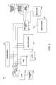
- FIG. 2shows a simplified block diagram of an integrated circuit 200 that incorporates the metal-programmable transistors.
- the integrated circuit 200includes standard cells 235 , power cells 240 , and base cells 245 comprising the metal-programmable transistors, as described in the '263 application.
- Each standard cell 235is a group of transistors designed and configured to perform a predetermined function.
- a standard cell 235may be logic gates, buffers or memory elements.
- the physical layout of each standard cell 235is optimized to consume a minimal amount of area. To this end, each standard cell 235 only includes a minimal number of tightly configured transistors to implement its specific function.
- the power cells 240include voltage supply traces and ground traces. The traces of power cells 240 generally distribute power to their respective rows 250 1 , 250 2 . . . 250 Y .
- the power cells 240are generally interconnected to one another in columns in order to distribute power between the rows 250 1 , 250 2 . . . 250 Y .
- Each base cell 245includes transistors that have unconnected terminals which unlike the predetermined nature of the revision cells enable each base cell 245 to be programmed to implement more than one function.
- a single base cell 245may be programmed to implement various functions such as an inverter, a two input NAND gate, or a D flip-flop.
- each base cell 245includes a high voltage rail V DD , a low voltage rail V SS , several P-type transistors such as P-channel Metal Oxide Semiconductor Field Effect Transistors (MOSFET) M P1 , M P2 . . . M PX , and several N-type transistors such as N-channel MOSFETs M N1 , M N2 . . . M NX .
- MOSFETMetal Oxide Semiconductor Field Effect Transistors
- N-type transistorssuch as N-channel MOSFETs M N1 , M N2 . . . M NX .
- Each P-type MOSFET M P1 , M P2 . . . M PXincludes a source S P1 , S P2 . . .
- each N-type MOSFET M N1 , M N2 . . . M NXincludes a source S N1 , S N2 . . . S NX , a gate G N1 , G N2 .
- D N1 , D N2 . . . D NXwhich are initially not operatively coupled to a standard cell 235 , power V DD , ground V SS , a P-type MOSFET M P1 , M P2 . . . M PX , or another N-type MOSFET M N1 , M N2 . . . M NX .
- each base cell 245includes complementary pairs of P-type and N-type MOSFETs M P1 , M P2 . . . M PX , and M N1 , M N2 . . . M NX .
- CMOScomplementary metal oxide semiconductor
- FIG. 3 BA physical layout of the preferred base cell 245 is shown in FIG. 3 B.
- Each base cell 245is depicted in FIG. 3B as having a high voltage rail V DD , a low voltage rail V SS , a row of four P-type MOSFETs M P1 . . . M P4 , and a row of four N-type MOSFETs M N1 . . . M N4 .
- Each base cell 245is fabricated with several physical layers upon a P-type silicon substrate.
- each P-type MOSFET M P1 . . . M P4includes a n-well layer, an active layer, a poly layer, and a metal one layer that are separated by insulating layers.
- the n-well layerforms several n-wells 302 1 . . . 302 4 by doping the P-type substrate with negative dopants, and the active layer forms several active areas 304 1 . . . 304 4 over the n-wells 302 1 . . . 302 4 by removing a portion of a thick oxide layer (not-shown) in order to leave a thin oxide layer over the n-wells 302 1 . . . 302 4 .
- Each active area 304 1 . . . 304 4 over the n-wells 302 1 . . . 302 4essentially defines an area for a P-type MOSFET M P1 . . . M P4 .
- the poly layerincludes traces of poly-silicon that are deposited over the active areas 304 1 . . . 304 4 in order to form the gates G P1 . . . G P4 of the P-type MOSFETs M P1 . . . M P4 .
- the metal 1 layerincludes metal traces that are deposited over the previous layers.
- the metal 1 layerincludes metal traces 310 1 . . . 310 4 and 312 1 . . . 312 4 which are electrically coupled to the underlying poly-silicon with contacts in order to form terminals for the gates G P1 . . . G P4 of the P-type MOSFETs M P1 . . . M P4 .
- the metal 1 layerincludes metal traces 320 1 . . . 320 4 and 322 1 . . . 322 4 which are electrically coupled to the underlying n-wells 302 1 . . . 302 4 with contacts in order to form terminals for the sources S P1 . .
- the metal 1 layeralso includes metal traces 330 1 . . . 330 4 and 332 1 . . . 332 4 which are electrically coupled to the underlying n-wells 302 1 . . . 302 4 with contacts in order to form terminals for the drains D P1 . . . D P4 of the P-type MOSFETs M P1 . . . M P4 .
- the metal 1 layerincludes the high voltage rail V DD that distributes a high voltage (e.g. 2.8 volts) supplied by the power cells 240 to the base cells 245 .
- each N-type MOSFET M N1 . . . M N4includes an active layer, a poly layer, and a metal 1 layer that are separated by insulating layers.
- the active layerforms several active areas 308 1 . . . 308 4 in the P-type substrate by removing a portion of a thick oxide layer (not shown) in order to leave a thin oxide layer over the P-type substrate.
- Each active area over the P-type substrateessentially defines an area for a N-type MOSFET M N1 . . . M N4 .
- the poly layerincludes traces of poly-silicon that are deposited over the active areas 308 1 . . . 308 4 in order to form the gates G N1 . . . G N4 of the N-type MOSFETs M N1 . . . M N4 .
- the metal 1 layerincludes metal traces that are deposited over the previous layers.
- the metal 1 layerincludes metal traces 340 1 . . . 340 4 and 342 1 . . . 342 4 which are electrically coupled to the underlying poly-silicon with contacts in order to form terminals for the gates G N1 . . . G N4 of the N-type MOSFETs M N1 . . . M N4 .
- the metal 1 layerincludes metal traces 350 1 . . . 350 4 and 352 1 . . . 352 4 which are electrically coupled to the P-type substrate with contacts in order to form terminals for the sources S N1 . . .
- the metal 1 layeralso includes metal traces 360 1 . . . 360 4 and 362 1 . . . 362 4 which are electrically coupled to the P-type substrate with contacts in order to form terminals for the drains D N1 . . . D N4 of the N-type MOSFETs M N1 . . . M N4 .
- the metal 1 layerincludes the low voltage rail V SS that distributes a low voltage (e.g. 0 volts) supplied by the power cells 240 to the base cells 245 .
- the function of the integrated circuit 200may be revised by (i) programming the various base cells 245 to implement various functions, and (ii) interconnecting the programmed base cells 245 to the standard cells 235 .
- a metal 2 layer of conductor traces along with additional traces in the metal 1 layermay be added to the base cells 245 in order to program the base cells 245 and interconnect the base cells 245 with the standard cells 235 .
- these additional tracescouple the terminals of the MOSFETs M P1 . . . M P4 , and M N1 . . . M N4 in order to implement functional units.
- These functional unitsmay then coupled to the standard cells 235 in order to revise, update, correct, or otherwise modify the function of the integrated circuit 200 .
- each base cell 245can be programmed to perform any one of a plurality of functions such as an inverter, an AND gate, an OR gate, a NAND gate, a NOR gate, a XOR gate, a XNOR gate, or a D flip-flop. It should be noted that a single base cell 245 may be programmed to perform more than one function (e.g. a single base cell 245 may be programmed to simultaneously implement a two input NAND gate and an inverter). Furthermore, it should be noted that multiple base cells 245 may be interconnected in order to perform larger functions (e.g.
- base cells 245may be interconnected in order to implement a 4 bit counter).
- the base cells 245may be added to the integrated circuit 200 without concern for future function needs unlike the revision cells. Accordingly, revisions to the integrated circuit 200 may be made to the extent base cells 245 are available.
- base cells 245are inserted into the circuit design layout wherever there is an unused area in the circuit, instead of just placing the base cells 245 at the ends of cell rows or at predesignated places on the circuit.
- an area-based placement/routing toolis used to insert the base cells 245 at unused areas in the circuit to create “ponds” of gates (POG) in many different parts of the circuit by using the base cells 245 .
- the placement of the POGsare not limited to designated areas in the circuit.
- FIG. 4illustrates a circuit with unused areas 401 , 402 , 403 , 404 , 405 and 406 existing next to areas occupied by standard cells.
- the area-based placement/routing toolextracts the unused areas 401 - 406 and then inserts POGs 411 , 412 , 413 , 414 , 415 and 416 into unused areas 401 - 406 , respectively, as shown in FIG. 4 A.
- the POGs 411 - 416are inserted into empty areas after the final standard cell area placement and routing is completed.
- the area-based placement/routing toolinserts the POGs 411 - 416 after the initial netlist is routed.
- the cost to implement the POGsare very minimal since the placement takes place after completing final standard cell placement and routing.
- each of the POGs 411 - 416contains different numbers of the metal-programmable complementary pairs of MOSFETs.
- the number of transistors contained in each of the POGs 411 - 416depends on the size of each of the unused areas 401 - 406 .
- each base cell 245(i) could be implemented with only one type of transistor (e.g. N-type MOSFETs), (ii) could be implemented with other kinds of transistors (e.g. bipolar junction transistors, BJTs, and junction field effect transistors, JFETs), or (iii)-could be implemented with a mix of transistors (e.g. BJTs and MOSFETs).
- the base cell 245could be implemented with only N-type MOSFETs thus enabling easy implementation of NMOS logic which is faster than CMOS logic.
- the metal-programmable transistorsmay be programmed to implement different types of cells that may be needed for the design changes, as explained above.
- the design changescan be implemented by making changes only to the upper layer masks.
- the embodiments of the present inventionare more likely to meet critical timing requirements if design changes are implemented because of the close proximity of the POGs to the standard cells that may need design changes.
- the POGsare placed at any unused areas in the circuit instead of being placed just at the ends of cell rows or at predesignated places. Therefore, the POGs are located in close proximity to the standard cells.
- FIG. 5is block diagram of a general purpose computer system, representing one of many suitable computer platforms for implementing the methods described above.
- FIG. 5shows a general purpose computer system 450 in accordance with the present invention. As shown in FIG.
- computer system 450includes a central processing unit (CPU) 452 , read-only memory (ROM) 454 , random access memory (RAM) 456 , expansion RAM 458 , inpuvoutput (I/O) circuitry 460 , display assembly 462 , input device 464 , and expansion bus 466 .
- Computer system 450may also optionally include a mass storage unit 468 such as a disk drive unit or nonvolatile memory such as flash memory and a real-time clock 470 .
- CPU 452is coupled to ROM 454 by a data bus 472 , control bus 474 , and address bus 476 .
- ROM 454contains the basic operating system for the computer system 450 .
- CPU 452is also connected to RAM 456 by busses 472 , 474 , and 476 .
- Expansion RAM 458is optionally coupled to RAM 456 for use by CPU 452 .
- CPU 452is also coupled to the I/O circuitry 460 by data bus 472 , control bus 474 , and address bus 476 to permit data transfers with peripheral devices.
- I/O circuitry 460typically includes a number of latches, registers and direct memory access (DMA) controllers. The purpose of I/O circuitry 460 is to provide an interface between CPU 452 and such peripheral devices as display assembly 462 , input device 464 , and mass storage 468 .
- DMAdirect memory access
- Display assembly 462 of computer system 450is an output device coupled to I/O circuitry 460 by a data bus 478 .
- Display assembly 462receives data from I/O circuitry 460 via bus 478 and displays that data on a suitable screen.
- the screen for display assembly 462can be a device that uses a cathode-ray tube (CRT), liquid crystal display (LCD), or the like, of the types commercially available from a variety of manufacturers.
- Input device 464can be a keyboard, a mouse, a stylus working in cooperation with a position-sensing display, or the like.
- the aforementioned input devicesare available from a variety of vendors and are well known in the art.
- mass storage 468is generally considered desirable. However, mass storage 468 can be eliminated by providing a sufficient mount of RAM 456 and expansion RAM 458 to store user application programs and data. In that case, RAMs 456 and 458 can optionally be provided with a backup battery to prevent the loss of data even when computer system 450 is turned off. However, it is generally desirable to have some type of long term mass storage 468 such as a commercially available hard disk drive, nonvolatile memory such as flash memory, battery backed RAM, PC-data cards, or the like.
- a removable storage read/write device 469may be coupled to I/O circuitry 460 to read from and to write to a removable storage media 471 .
- Removable storage media 471may represent, for example, a magnetic disk, a magnetic tape, an opto-magnetic disk, an optical disk, or the like. Instructions for implementing the inventive method may be provided, in one embodiment, to a network via such a removable storage media.
- CPU 452In operation, information is input into the computer system 450 by typing on a keyboard, manipulating a mouse or trackball, or “writing” on a tablet or on position-sensing screen of display assembly 462 .
- CPU 452then processes the data under control of an operating system and an application program, such as a program to perform steps of the inventive method described above, stored in ROM 454 and/or RAM 456 .
- CPU 452then typically produces data which is output to the display assembly 462 to produce appropriate images on its screen.
- Expansion bus 466is coupled to data bus 472 , control bus 474 , and address bus 476 . Expansion bus 466 provides extra ports to couple devices such as network interface circuits, modems, display switches, microphones, speakers, etc. to CPU 452 . Network communication is accomplished through the network interface circuit and an appropriate network.
- Suitable computers for use in implementing the present inventionmay be obtained from various vendors. Various computers, however, may be used depending upon the size and complexity of the OPC tasks. Suitable computers include mainframe computers, multiprocessor computers, workstations or personal computers. In addition, although a general purpose computer system has been described above, a special-purpose computer may also be used.
- the present inventionalso relates to machine readable media on which are stored program instructions for performing the methods of this invention.
- Such mediaincludes, by way of example, magnetic disks, magnetic tape, optically readable media such as CD ROMs, semiconductor memory such as PCMCIA cards, etc.
- the mediummay take the form of a portable item such as a small disk, diskette, cassette, etc., or it may take the form of a relatively larger or immobile item such as a hard disk drive or RAM provided in a computer.
Landscapes
- Engineering & Computer Science (AREA)
- Computer Hardware Design (AREA)
- Physics & Mathematics (AREA)
- Theoretical Computer Science (AREA)
- Architecture (AREA)
- Evolutionary Computation (AREA)
- Geometry (AREA)
- General Engineering & Computer Science (AREA)
- General Physics & Mathematics (AREA)
- Design And Manufacture Of Integrated Circuits (AREA)
Abstract
Description
Claims (21)
Priority Applications (1)
| Application Number | Priority Date | Filing Date | Title |
|---|---|---|---|
| US09/493,467US6446248B1 (en) | 2000-01-28 | 2000-01-28 | Spare cells placement methodology |
Applications Claiming Priority (1)
| Application Number | Priority Date | Filing Date | Title |
|---|---|---|---|
| US09/493,467US6446248B1 (en) | 2000-01-28 | 2000-01-28 | Spare cells placement methodology |
Publications (1)
| Publication Number | Publication Date |
|---|---|
| US6446248B1true US6446248B1 (en) | 2002-09-03 |
Family
ID=23960331
Family Applications (1)
| Application Number | Title | Priority Date | Filing Date |
|---|---|---|---|
| US09/493,467Expired - LifetimeUS6446248B1 (en) | 2000-01-28 | 2000-01-28 | Spare cells placement methodology |
Country Status (1)
| Country | Link |
|---|---|
| US (1) | US6446248B1 (en) |
Cited By (28)
| Publication number | Priority date | Publication date | Assignee | Title |
|---|---|---|---|---|
| US20030233625A1 (en)* | 2002-06-18 | 2003-12-18 | Ip-First, Llc. | Method for allocating spare cells in auto-place-route blocks |
| US20040031007A1 (en)* | 2002-08-07 | 2004-02-12 | Mitsubishi Denki Kabushiki Kaisha | Automatic placement and routing apparatus automatically inserting a capacitive cell |
| US20040060034A1 (en)* | 2002-09-23 | 2004-03-25 | Numerical Technologies, Inc. | Accelerated layout processing using OPC pre-processing |
| US20040080334A1 (en)* | 2002-10-25 | 2004-04-29 | Alain Vergnes | Spare cell architecture for fixing design errors in manufactured integrated circuits |
| US20040199879A1 (en)* | 2003-04-04 | 2004-10-07 | Bradfield Travis Alister | System and method for achieving timing closure in fixed placed designs after implementing logic changes |
| US20040205282A1 (en)* | 2003-04-08 | 2004-10-14 | Solomon Richard L. | Methods and systems for improving delayed read handling |
| US20050033434A1 (en)* | 2003-08-06 | 2005-02-10 | Sdgi Holdings, Inc. | Posterior elements motion restoring device |
| US20050120321A1 (en)* | 2003-12-01 | 2005-06-02 | Lsi Logic Corporation | Integrated circuits, and design and manufacture thereof |
| US20050116738A1 (en)* | 2003-12-01 | 2005-06-02 | Lsi Logic Corporation | Integrated circuits, and design and manufacture thereof |
| US20050172253A1 (en)* | 2004-01-30 | 2005-08-04 | Nec Electronics Corporation | Automatic placement and routing device, method for placement and routing of semiconductor device, semiconductor device and manufacturing method of the same |
| US20050229133A1 (en)* | 2004-03-30 | 2005-10-13 | Oki Electric Industry Co., Ltd. | Method of designing a circuit of a semiconductor device |
| US7007259B2 (en) | 2003-07-31 | 2006-02-28 | Lsi Logic Corporation | Method for providing clock-net aware dummy metal using dummy regions |
| US20060123373A1 (en)* | 2004-12-08 | 2006-06-08 | Lsi Logic Corporation | Density driven layout for RRAM configuration module |
| US20060181307A1 (en)* | 2005-02-14 | 2006-08-17 | Kenichi Shibayashi | Semiconductor integrated circuit and method for laying-out and wiring the semiconductor integrated circuit |
| US7215004B1 (en)* | 2004-07-01 | 2007-05-08 | Netlogic Microsystems, Inc. | Integrated circuit device with electronically accessible device identifier |
| US20080005712A1 (en)* | 2006-06-29 | 2008-01-03 | Charlebois Steven E | Method of optimizing customizable filler cells in an integrated circuit physical design process |
| US20090013297A1 (en)* | 2006-05-24 | 2009-01-08 | Texas Instruments Incorporated | Contact resistance and capacitance for semiconductor devices |
| US20090172608A1 (en)* | 2007-12-28 | 2009-07-02 | Hopkins Jeremy T | Techniques for Selecting Spares to Implement a Design Change in an Integrated Circuit |
| US20090250820A1 (en)* | 2004-07-01 | 2009-10-08 | Dimitri Argyres | Configurable non-volatile logic structure for characterizing an integrated circuit device |
| US20090259981A1 (en)* | 2008-04-09 | 2009-10-15 | Shibashish Patel | Integrated Circuit With Areas Having Uniform Voltage Drop and Method Therefor |
| US20110072407A1 (en)* | 2009-09-18 | 2011-03-24 | International Business Machines Corporation | Automatic Positioning of Gate Array Circuits in an Integrated Circuit Design |
| US8234612B2 (en) | 2010-08-25 | 2012-07-31 | International Business Machines Corporation | Cone-aware spare cell placement using hypergraph connectivity analysis |
| US8448100B1 (en) | 2012-04-11 | 2013-05-21 | Taiwan Semiconductor Manufacturing Co., Ltd. | Tool and method for eliminating multi-patterning conflicts |
| US8875084B1 (en) | 2013-07-18 | 2014-10-28 | International Business Machines Corporation | Optimal spare latch selection for metal-only ECOs |
| US9436792B2 (en) | 2014-08-22 | 2016-09-06 | Samsung Electronics Co., Ltd. | Method of designing layout of integrated circuit and method of manufacturing integrated circuit |
| US9953121B2 (en) | 2016-05-03 | 2018-04-24 | International Business Machines Corporation | Accommodating engineering change orders in integrated circuit design |
| US20190147132A1 (en)* | 2016-09-30 | 2019-05-16 | Taiwan Semiconductor Manufacturing Company, Ltd. | Semiconductor device having engineering change order (eco) cells |
| US10817640B2 (en) | 2018-11-09 | 2020-10-27 | Samsung Electronics Co., Ltd. | Integrated circuit including different types of cells, and method and system of designing the same |
Citations (3)
| Publication number | Priority date | Publication date | Assignee | Title |
|---|---|---|---|---|
| US5361041A (en)* | 1993-06-17 | 1994-11-01 | Unitrode Corporation | Push-pull amplifier |
| US6002861A (en)* | 1988-10-05 | 1999-12-14 | Quickturn Design Systems, Inc. | Method for performing simulation using a hardware emulation system |
| US6226775B1 (en)* | 1997-08-25 | 2001-05-01 | Nec Corporation | Semiconductor integrated circuit designing method of an interconnection thereof and recording medium in which the method is recorded for empty area |
- 2000
- 2000-01-28USUS09/493,467patent/US6446248B1/ennot_activeExpired - Lifetime
Patent Citations (3)
| Publication number | Priority date | Publication date | Assignee | Title |
|---|---|---|---|---|
| US6002861A (en)* | 1988-10-05 | 1999-12-14 | Quickturn Design Systems, Inc. | Method for performing simulation using a hardware emulation system |
| US5361041A (en)* | 1993-06-17 | 1994-11-01 | Unitrode Corporation | Push-pull amplifier |
| US6226775B1 (en)* | 1997-08-25 | 2001-05-01 | Nec Corporation | Semiconductor integrated circuit designing method of an interconnection thereof and recording medium in which the method is recorded for empty area |
Cited By (50)
| Publication number | Priority date | Publication date | Assignee | Title |
|---|---|---|---|---|
| US20030233625A1 (en)* | 2002-06-18 | 2003-12-18 | Ip-First, Llc. | Method for allocating spare cells in auto-place-route blocks |
| US6993738B2 (en)* | 2002-06-18 | 2006-01-31 | Ip-First, Llc | Method for allocating spare cells in auto-place-route blocks |
| US20040031007A1 (en)* | 2002-08-07 | 2004-02-12 | Mitsubishi Denki Kabushiki Kaisha | Automatic placement and routing apparatus automatically inserting a capacitive cell |
| US6978431B2 (en)* | 2002-08-07 | 2005-12-20 | Renesas Technology Corp. | Automatic placement and routing apparatus automatically inserting a capacitive cell |
| US20040060034A1 (en)* | 2002-09-23 | 2004-03-25 | Numerical Technologies, Inc. | Accelerated layout processing using OPC pre-processing |
| US6807663B2 (en)* | 2002-09-23 | 2004-10-19 | Numerical Technologies, Inc. | Accelerated layout processing using OPC pre-processing |
| US20040080334A1 (en)* | 2002-10-25 | 2004-04-29 | Alain Vergnes | Spare cell architecture for fixing design errors in manufactured integrated circuits |
| US6791355B2 (en)* | 2002-10-25 | 2004-09-14 | Atmel Corporation | Spare cell architecture for fixing design errors in manufactured integrated circuits |
| US20040199879A1 (en)* | 2003-04-04 | 2004-10-07 | Bradfield Travis Alister | System and method for achieving timing closure in fixed placed designs after implementing logic changes |
| US6922817B2 (en)* | 2003-04-04 | 2005-07-26 | Lsi Logic Corporation | System and method for achieving timing closure in fixed placed designs after implementing logic changes |
| US20040205282A1 (en)* | 2003-04-08 | 2004-10-14 | Solomon Richard L. | Methods and systems for improving delayed read handling |
| US7216194B2 (en) | 2003-04-08 | 2007-05-08 | Lsi Logic Corporation | Methods and systems for improving delayed read handling |
| US7007259B2 (en) | 2003-07-31 | 2006-02-28 | Lsi Logic Corporation | Method for providing clock-net aware dummy metal using dummy regions |
| US20050033434A1 (en)* | 2003-08-06 | 2005-02-10 | Sdgi Holdings, Inc. | Posterior elements motion restoring device |
| US20050116738A1 (en)* | 2003-12-01 | 2005-06-02 | Lsi Logic Corporation | Integrated circuits, and design and manufacture thereof |
| US20050120321A1 (en)* | 2003-12-01 | 2005-06-02 | Lsi Logic Corporation | Integrated circuits, and design and manufacture thereof |
| US7032190B2 (en)* | 2003-12-01 | 2006-04-18 | Lsi Logic Corporation | Integrated circuits, and design and manufacture thereof |
| US20050172253A1 (en)* | 2004-01-30 | 2005-08-04 | Nec Electronics Corporation | Automatic placement and routing device, method for placement and routing of semiconductor device, semiconductor device and manufacturing method of the same |
| US20050229133A1 (en)* | 2004-03-30 | 2005-10-13 | Oki Electric Industry Co., Ltd. | Method of designing a circuit of a semiconductor device |
| US7716626B2 (en)* | 2004-03-30 | 2010-05-11 | Oki Semiconductor Co., Ltd. | Method of designing a circuit layout of a semiconductor device |
| US7943400B2 (en) | 2004-07-01 | 2011-05-17 | Netlogic Microsystems, Inc. | Integrated circuit device with electronically accessible device identifier |
| US7215004B1 (en)* | 2004-07-01 | 2007-05-08 | Netlogic Microsystems, Inc. | Integrated circuit device with electronically accessible device identifier |
| US20070287229A1 (en)* | 2004-07-01 | 2007-12-13 | Nataraj Bindiganavale S | Integrated circuit device with electronically accessible device identifier |
| US20090250820A1 (en)* | 2004-07-01 | 2009-10-08 | Dimitri Argyres | Configurable non-volatile logic structure for characterizing an integrated circuit device |
| US7868383B2 (en)* | 2004-07-01 | 2011-01-11 | Netlogic Microsystems, Inc. | Configurable non-volatile logic structure for characterizing an integrated circuit device |
| US7246337B2 (en)* | 2004-12-08 | 2007-07-17 | Lsi Corporation | Density driven layout for RRAM configuration module |
| US7818703B2 (en) | 2004-12-08 | 2010-10-19 | Lsi Corporation | Density driven layout for RRAM configuration module |
| US20060123373A1 (en)* | 2004-12-08 | 2006-06-08 | Lsi Logic Corporation | Density driven layout for RRAM configuration module |
| US20060181307A1 (en)* | 2005-02-14 | 2006-08-17 | Kenichi Shibayashi | Semiconductor integrated circuit and method for laying-out and wiring the semiconductor integrated circuit |
| US8112737B2 (en)* | 2006-05-24 | 2012-02-07 | Texas Instruments Incorporated | Contact resistance and capacitance for semiconductor devices |
| US20090013297A1 (en)* | 2006-05-24 | 2009-01-08 | Texas Instruments Incorporated | Contact resistance and capacitance for semiconductor devices |
| US20080005712A1 (en)* | 2006-06-29 | 2008-01-03 | Charlebois Steven E | Method of optimizing customizable filler cells in an integrated circuit physical design process |
| US7444609B2 (en) | 2006-06-29 | 2008-10-28 | International Business Machines Corporation | Method of optimizing customizable filler cells in an integrated circuit physical design process |
| US20090172608A1 (en)* | 2007-12-28 | 2009-07-02 | Hopkins Jeremy T | Techniques for Selecting Spares to Implement a Design Change in an Integrated Circuit |
| US8166439B2 (en) | 2007-12-28 | 2012-04-24 | International Business Machines Corporation | Techniques for selecting spares to implement a design change in an integrated circuit |
| US8959470B2 (en)* | 2008-04-09 | 2015-02-17 | Advanced Micro Devices, Inc. | Integrated circuit with areas having uniform voltage drop and method therefor |
| US20090259981A1 (en)* | 2008-04-09 | 2009-10-15 | Shibashish Patel | Integrated Circuit With Areas Having Uniform Voltage Drop and Method Therefor |
| US20110072407A1 (en)* | 2009-09-18 | 2011-03-24 | International Business Machines Corporation | Automatic Positioning of Gate Array Circuits in an Integrated Circuit Design |
| US8276105B2 (en) | 2009-09-18 | 2012-09-25 | International Business Machines Corporation | Automatic positioning of gate array circuits in an integrated circuit design |
| US8234612B2 (en) | 2010-08-25 | 2012-07-31 | International Business Machines Corporation | Cone-aware spare cell placement using hypergraph connectivity analysis |
| US8448100B1 (en) | 2012-04-11 | 2013-05-21 | Taiwan Semiconductor Manufacturing Co., Ltd. | Tool and method for eliminating multi-patterning conflicts |
| US8875084B1 (en) | 2013-07-18 | 2014-10-28 | International Business Machines Corporation | Optimal spare latch selection for metal-only ECOs |
| US9436792B2 (en) | 2014-08-22 | 2016-09-06 | Samsung Electronics Co., Ltd. | Method of designing layout of integrated circuit and method of manufacturing integrated circuit |
| US9953121B2 (en) | 2016-05-03 | 2018-04-24 | International Business Machines Corporation | Accommodating engineering change orders in integrated circuit design |
| US9965576B2 (en) | 2016-05-03 | 2018-05-08 | International Business Machines Corporation | Accommodating engineering change orders in integrated circuit design |
| US20190147132A1 (en)* | 2016-09-30 | 2019-05-16 | Taiwan Semiconductor Manufacturing Company, Ltd. | Semiconductor device having engineering change order (eco) cells |
| US10678977B2 (en)* | 2016-09-30 | 2020-06-09 | Taiwan Semiconductor Manufacturing Company, Ltd. | Semiconductor device having engineering change order (ECO) cells |
| US10970440B2 (en)* | 2016-09-30 | 2021-04-06 | Taiwan Semiconductor Manufacturing Company, Ltd. | Method and system for generating layout diagram for semiconductor device having engineering change order (ECO) cells |
| US11842131B2 (en) | 2016-09-30 | 2023-12-12 | Taiwan Semiconductor Manufacturing Company, Ltd. | Method and system for generating layout diagram for semiconductor device having engineering change order (ECO) cells |
| US10817640B2 (en) | 2018-11-09 | 2020-10-27 | Samsung Electronics Co., Ltd. | Integrated circuit including different types of cells, and method and system of designing the same |
Similar Documents
| Publication | Publication Date | Title |
|---|---|---|
| US6446248B1 (en) | Spare cells placement methodology | |
| US8132142B2 (en) | Various methods and apparatuses to route multiple power rails to a cell | |
| US7137094B2 (en) | Method for reducing layers revision in engineering change order | |
| US4701778A (en) | Semiconductor integrated circuit having overlapping circuit cells and method for designing circuit pattern therefor | |
| US6453447B1 (en) | Method for fabricating integrated circuits | |
| US7269803B2 (en) | System and method for mapping logical components to physical locations in an integrated circuit design environment | |
| US6714903B1 (en) | Placement and routing of circuits using a combined processing/buffer cell | |
| US20140229908A1 (en) | Power Routing in Standard Cells | |
| US12147750B2 (en) | Multiplexer | |
| US5369595A (en) | Method of combining gate array and standard cell circuits on a common semiconductor chip | |
| US6327696B1 (en) | Method and apparatus for zero skew routing from a fixed H trunk | |
| US6820048B1 (en) | 4 point derating scheme for propagation delay and setup/hold time computation | |
| US6484297B1 (en) | 4K derating scheme for propagation delay and setup/hold time computation | |
| TWI771698B (en) | Multiplexer circuit, multiplexer and method for manufacturing multiplexer | |
| US6243849B1 (en) | Method and apparatus for netlist filtering and cell placement | |
| US6925615B2 (en) | Semiconductor device having embedded array | |
| US11092885B2 (en) | Manufacturing methods of semiconductor devices | |
| US20030023946A1 (en) | Standard cell library generation using merged power method | |
| KR20020042507A (en) | A semiconductor device, a method of manufacturing the same and storage media | |
| US6530063B1 (en) | Method and apparatus for detecting equivalent and anti-equivalent pins | |
| US6519746B1 (en) | Method and apparatus for minimization of net delay by optimal buffer insertion | |
| US20120159412A1 (en) | Transistor-level layout synthesis | |
| US6536016B1 (en) | Method and apparatus for locating constants in combinational circuits | |
| Chavez-Martinez et al. | Modified standard cell methodology for VLSI layout compaction | |
| AUTOMATION | ALGORITHMS FOR VLSI PHYSICAL DESIGN AUTOMATION THIRD EDITION |
Legal Events
| Date | Code | Title | Description |
|---|---|---|---|
| AS | Assignment | Owner name:LSI LOGIC CORPORATION, CALIFORNIA Free format text:ASSIGNMENT OF ASSIGNORS INTEREST;ASSIGNORS:SOLOMON, RICHARD L.;SMITH, PAUL J.;REEL/FRAME:010555/0229 Effective date:20000124 | |
| STCF | Information on status: patent grant | Free format text:PATENTED CASE | |
| FPAY | Fee payment | Year of fee payment:4 | |
| FEPP | Fee payment procedure | Free format text:PAYOR NUMBER ASSIGNED (ORIGINAL EVENT CODE: ASPN); ENTITY STATUS OF PATENT OWNER: LARGE ENTITY | |
| FPAY | Fee payment | Year of fee payment:8 | |
| FPAY | Fee payment | Year of fee payment:12 | |
| AS | Assignment | Owner name:DEUTSCHE BANK AG NEW YORK BRANCH, AS COLLATERAL AG Free format text:PATENT SECURITY AGREEMENT;ASSIGNORS:LSI CORPORATION;AGERE SYSTEMS LLC;REEL/FRAME:032856/0031 Effective date:20140506 | |
| AS | Assignment | Owner name:LSI CORPORATION, CALIFORNIA Free format text:CHANGE OF NAME;ASSIGNOR:LSI LOGIC CORPORATION;REEL/FRAME:033102/0270 Effective date:20070406 | |
| AS | Assignment | Owner name:AVAGO TECHNOLOGIES GENERAL IP (SINGAPORE) PTE. LTD Free format text:ASSIGNMENT OF ASSIGNORS INTEREST;ASSIGNOR:LSI CORPORATION;REEL/FRAME:035390/0388 Effective date:20140814 | |
| AS | Assignment | Owner name:AGERE SYSTEMS LLC, PENNSYLVANIA Free format text:TERMINATION AND RELEASE OF SECURITY INTEREST IN PATENT RIGHTS (RELEASES RF 032856-0031);ASSIGNOR:DEUTSCHE BANK AG NEW YORK BRANCH, AS COLLATERAL AGENT;REEL/FRAME:037684/0039 Effective date:20160201 Owner name:LSI CORPORATION, CALIFORNIA Free format text:TERMINATION AND RELEASE OF SECURITY INTEREST IN PATENT RIGHTS (RELEASES RF 032856-0031);ASSIGNOR:DEUTSCHE BANK AG NEW YORK BRANCH, AS COLLATERAL AGENT;REEL/FRAME:037684/0039 Effective date:20160201 | |
| AS | Assignment | Owner name:BANK OF AMERICA, N.A., AS COLLATERAL AGENT, NORTH CAROLINA Free format text:PATENT SECURITY AGREEMENT;ASSIGNOR:AVAGO TECHNOLOGIES GENERAL IP (SINGAPORE) PTE. LTD.;REEL/FRAME:037808/0001 Effective date:20160201 Owner name:BANK OF AMERICA, N.A., AS COLLATERAL AGENT, NORTH Free format text:PATENT SECURITY AGREEMENT;ASSIGNOR:AVAGO TECHNOLOGIES GENERAL IP (SINGAPORE) PTE. LTD.;REEL/FRAME:037808/0001 Effective date:20160201 | |
| AS | Assignment | Owner name:AVAGO TECHNOLOGIES GENERAL IP (SINGAPORE) PTE. LTD., SINGAPORE Free format text:TERMINATION AND RELEASE OF SECURITY INTEREST IN PATENTS;ASSIGNOR:BANK OF AMERICA, N.A., AS COLLATERAL AGENT;REEL/FRAME:041710/0001 Effective date:20170119 Owner name:AVAGO TECHNOLOGIES GENERAL IP (SINGAPORE) PTE. LTD Free format text:TERMINATION AND RELEASE OF SECURITY INTEREST IN PATENTS;ASSIGNOR:BANK OF AMERICA, N.A., AS COLLATERAL AGENT;REEL/FRAME:041710/0001 Effective date:20170119 | |
| AS | Assignment | Owner name:BELL SEMICONDUCTOR, LLC, ILLINOIS Free format text:ASSIGNMENT OF ASSIGNORS INTEREST;ASSIGNORS:AVAGO TECHNOLOGIES GENERAL IP (SINGAPORE) PTE. LTD.;BROADCOM CORPORATION;REEL/FRAME:044887/0109 Effective date:20171208 | |
| AS | Assignment | Owner name:CORTLAND CAPITAL MARKET SERVICES LLC, AS COLLATERA Free format text:SECURITY INTEREST;ASSIGNORS:HILCO PATENT ACQUISITION 56, LLC;BELL SEMICONDUCTOR, LLC;BELL NORTHERN RESEARCH, LLC;REEL/FRAME:045216/0020 Effective date:20180124 | |
| AS | Assignment | Owner name:BELL NORTHERN RESEARCH, LLC, ILLINOIS Free format text:RELEASE BY SECURED PARTY;ASSIGNOR:CORTLAND CAPITAL MARKET SERVICES LLC;REEL/FRAME:059720/0223 Effective date:20220401 Owner name:BELL SEMICONDUCTOR, LLC, ILLINOIS Free format text:RELEASE BY SECURED PARTY;ASSIGNOR:CORTLAND CAPITAL MARKET SERVICES LLC;REEL/FRAME:059720/0223 Effective date:20220401 Owner name:HILCO PATENT ACQUISITION 56, LLC, ILLINOIS Free format text:RELEASE BY SECURED PARTY;ASSIGNOR:CORTLAND CAPITAL MARKET SERVICES LLC;REEL/FRAME:059720/0223 Effective date:20220401 |