US6445554B1 - Method and system for providing edge-junction TMR for high areal density magnetic recording - Google Patents
Method and system for providing edge-junction TMR for high areal density magnetic recordingDownload PDFInfo
- Publication number
- US6445554B1 US6445554B1US09/523,025US52302500AUS6445554B1US 6445554 B1US6445554 B1US 6445554B1US 52302500 AUS52302500 AUS 52302500AUS 6445554 B1US6445554 B1US 6445554B1
- Authority
- US
- United States
- Prior art keywords
- layer
- pinned
- tmr
- free layer
- tmr sensor
- Prior art date
- Legal status (The legal status is an assumption and is not a legal conclusion. Google has not performed a legal analysis and makes no representation as to the accuracy of the status listed.)
- Expired - Lifetime
Links
Images


Classifications
- G—PHYSICS
- G11—INFORMATION STORAGE
- G11B—INFORMATION STORAGE BASED ON RELATIVE MOVEMENT BETWEEN RECORD CARRIER AND TRANSDUCER
- G11B5/00—Recording by magnetisation or demagnetisation of a record carrier; Reproducing by magnetic means; Record carriers therefor
- G11B5/127—Structure or manufacture of heads, e.g. inductive
- G11B5/33—Structure or manufacture of flux-sensitive heads, i.e. for reproduction only; Combination of such heads with means for recording or erasing only
- G11B5/39—Structure or manufacture of flux-sensitive heads, i.e. for reproduction only; Combination of such heads with means for recording or erasing only using magneto-resistive devices or effects
- G11B5/3903—Structure or manufacture of flux-sensitive heads, i.e. for reproduction only; Combination of such heads with means for recording or erasing only using magneto-resistive devices or effects using magnetic thin film layers or their effects, the films being part of integrated structures
- G11B5/3906—Details related to the use of magnetic thin film layers or to their effects
- G11B5/3929—Disposition of magnetic thin films not used for directly coupling magnetic flux from the track to the MR film or for shielding
- G11B5/3932—Magnetic biasing films
- B—PERFORMING OPERATIONS; TRANSPORTING
- B82—NANOTECHNOLOGY
- B82Y—SPECIFIC USES OR APPLICATIONS OF NANOSTRUCTURES; MEASUREMENT OR ANALYSIS OF NANOSTRUCTURES; MANUFACTURE OR TREATMENT OF NANOSTRUCTURES
- B82Y10/00—Nanotechnology for information processing, storage or transmission, e.g. quantum computing or single electron logic
- B—PERFORMING OPERATIONS; TRANSPORTING
- B82—NANOTECHNOLOGY
- B82Y—SPECIFIC USES OR APPLICATIONS OF NANOSTRUCTURES; MEASUREMENT OR ANALYSIS OF NANOSTRUCTURES; MANUFACTURE OR TREATMENT OF NANOSTRUCTURES
- B82Y25/00—Nanomagnetism, e.g. magnetoimpedance, anisotropic magnetoresistance, giant magnetoresistance or tunneling magnetoresistance
- G—PHYSICS
- G11—INFORMATION STORAGE
- G11B—INFORMATION STORAGE BASED ON RELATIVE MOVEMENT BETWEEN RECORD CARRIER AND TRANSDUCER
- G11B5/00—Recording by magnetisation or demagnetisation of a record carrier; Reproducing by magnetic means; Record carriers therefor
- G11B5/127—Structure or manufacture of heads, e.g. inductive
- G11B5/33—Structure or manufacture of flux-sensitive heads, i.e. for reproduction only; Combination of such heads with means for recording or erasing only
- G11B5/39—Structure or manufacture of flux-sensitive heads, i.e. for reproduction only; Combination of such heads with means for recording or erasing only using magneto-resistive devices or effects
- G11B5/3903—Structure or manufacture of flux-sensitive heads, i.e. for reproduction only; Combination of such heads with means for recording or erasing only using magneto-resistive devices or effects using magnetic thin film layers or their effects, the films being part of integrated structures
- G11B5/3906—Details related to the use of magnetic thin film layers or to their effects
- G11B5/3909—Arrangements using a magnetic tunnel junction
- G—PHYSICS
- G11—INFORMATION STORAGE
- G11B—INFORMATION STORAGE BASED ON RELATIVE MOVEMENT BETWEEN RECORD CARRIER AND TRANSDUCER
- G11B5/00—Recording by magnetisation or demagnetisation of a record carrier; Reproducing by magnetic means; Record carriers therefor
- G11B5/127—Structure or manufacture of heads, e.g. inductive
- G11B5/33—Structure or manufacture of flux-sensitive heads, i.e. for reproduction only; Combination of such heads with means for recording or erasing only
- G11B5/39—Structure or manufacture of flux-sensitive heads, i.e. for reproduction only; Combination of such heads with means for recording or erasing only using magneto-resistive devices or effects
- G11B5/3903—Structure or manufacture of flux-sensitive heads, i.e. for reproduction only; Combination of such heads with means for recording or erasing only using magneto-resistive devices or effects using magnetic thin film layers or their effects, the films being part of integrated structures
Definitions
- the present inventionrelates to magnetic recording, and more particularly to a method and system for providing a tunneling magnetoresistance recording junction suitable for high areal density magnetic recording.
- FIG. 1Adepicts diagrams of a conventional TMR sensor 10 as viewed from the side.
- FIG. 1Adepicts the shields first and second shields 24 and 26 , first and second gaps 20 and 22 , leads 11 and 19 , and the TMR sensor 10 .
- FIG. 1Bdepicts the conventional TMR sensor 10 as viewed from the side and from an air-bearing surface or magnetic material with which the TMR sensor 10 is being used.
- FIG. 1Bdepicts leads 11 and 19 and first and second gaps 20 and 22 , respectively.
- conventional shields 24 and 26Not depicted in FIG. 1B are conventional shields 24 and 26 , which partially surround the conventional TMR sensor 10 .
- the conventional TMR sensor 10includes a conventional antiferromagnetic (“AFM”) layer 12 , a conventional pinned layer 14 , a conventional barrier layer 16 , and a conventional free layer 18 .
- the TMR junction for the TMR sensor 10includes the interfaces between the conventional pinned layer 14 , the conventional barrier layer 16 and the conventional free layer 18 .
- the conventional pinned layer 14 and conventional free layer 18are ferromagnetic.
- the conventional pinned layer 14has its magnetization fixed, or pinned, in place because the conventional pinned layer 14 is magnetically coupled to the conventional AFM layer 12 .
- the conventional antiferromagnetic layer 12is approximately one hundred to three hundred Angstroms thick.
- the conventional pinned layer 14is approximately twenty to one hundred Angstroms thick.
- the conventional barrier layer 16is typically five to twenty Angstroms thick and the conventional free layer 18 is typically thirty to one hundred Angstroms thick.
- the magnetization of the conventional free layer 18 of the TMR sensor 10is biased in the plane of the page when there is no external magnetic field, but is free to rotate in response to an external magnetic field.
- the conventional free layer 18is typically composed of Co, Co 90 Fe 10 , or a bilayer of Co 90 Fe 10 and permalloy.
- the magnetization of the conventional pinned layer 14is pinned perpendicular to the plane of the page.
- the conventional pinned layer 14is typically composed of Co, Fe, or Ni.
- the conventional barrier layer 16is typically composed of aluminum oxide (Al 2 O 3 ).
- a bias currentis driven between the leads 11 and 19 , perpendicular to the plane of the layers 12 , 14 , 16 and 18 of the conventional TMR sensor 10 .
- the TMR sensor 10is known as a current perpendicular to the plane (“CPP”) junction.
- the direction of flow of the bias currentis depicted by the arrow 24 .
- the MR effect in the conventional TMR sensor 10is believed to be due to spin polarized tunneling of electrons between the conventional free layer 18 and the conventional pinned layer 14 .
- spin polarized electronstunnel through the conventional barrier layer 16 in order to provide the magnetoresistive effect.
- the resistance of the conventional TMR. sensor 10is minimized or maximized, respectively.
- the magnetization of the conventional free layer 18is biased to be perpendicular to the magnetization of the conventional pinned layer 14 when no external field is applied, as depicted in FIG. 1 B.
- the magnetoresistance, MR, of a MR sensoris the difference between the maximum resistance and the minimum resistance of the MR sensor.
- the MR ratio of the MR sensoris typically called ⁇ R/R, and is typically given as a percent.
- a typical magnetoresistance of the conventional TMR sensoris approximately twenty percent.
- the conventional TMR sensor 10is of interest for MR sensors for high areal density recording applications.
- higher recording densitiesfor example over 40 gigabits (“Gb”) per square inch.
- Gbgigabits
- the signal from the read sensor for a given magnetic fieldis desired to be increased.
- One mechanism for increasing this signalwould be to use an MR sensor having an increased MR ratio.
- the conventional TMR sensor 10has an MR of approximately twenty percent, which is higher than a conventional giant magnetoresistance (“GMR”) sensor having a nonmagnetic conducting layer separating a free layer and a pinned layer. Furthermore, the conventional TMR sensor 10 has a smaller thickness than a conventional GMR sensor, allowing for a smaller spacing between shields (not shown). The smaller spacing between shields allows for more effective shielding of bits not desired to be read by the TMR sensor 10 .
- the width of the TMR sensor 10shown in FIG. 1, can be narrower than a conventional GMR sensor. This also aids in allowing the conventional TMR sensor 10 to read smaller bits at higher recording densities.
- the conventional TMR sensor 10is of interest for high-density recording applications, one of ordinary skill in the art will readily realize that there are several drawbacks to the conventional TMR sensor 10 . Some of these drawbacks are due to the area of the conventional TMR sensor 10 . In particular, the conventional TMR sensor 10 often has a nonuniform bias current and may have a reduced MR ratio due to the large area of the TMR sensor 10 .
- the area of the conventional TMR junctionincludes the area of the interfaces between the conventional pinned layer 14 , the conventional free layer 18 and the conventional barrier layer 18 . The junction area is defined by the width of the conventional TMR sensor 10 , w, depicted in FIG.
- the length of the conventional TMR sensor 10is determined by the stripe height, h, of the conventional TMR sensor 10 as depicted in FIG. 1 A.
- the width w of the conventional TMR sensor 10is determined by the track width (not shown) of the media desired to be read and is typically approximately half of the track width.
- the junction area for the conventional TMR sensor 10is the width multiplied by the stripe height (w ⁇ h).
- the area of the conventional TMR junction for the conventional TMR sensor 10is typically on the order of one square micrometer.
- the conventional barrier layer 16is typically between five and twenty Angstroms thick.
- the conventional barrier layer 16has such a large area but is so thin, pinholes (not shown in FIG. 1) often exist in the conventional barrier layer 16 .
- Currentmore easily flows between the conventional pinned layer 14 and the conventional free layer 18 through these pinholes than through the conventional barrier layer 16 .
- the bias current between the leads 11 and 19is nonuniform.
- the MR effect for the conventional TMR sensor 10can be reduced by the electrons which pass through the pinholes instead of tunneling through the conventional barrier layer 16 . Consequently, not only may the bias current lack uniformity, but the MR ratio for the conventional TMR sensor 10 may also be reduced below the intrinsic percentage (approximately twenty percent).
- the conventional free layer 18 , the conventional barrier layer 16 and the conventional pinned layer 14are two metallic layers separated by an insulating layer. As a result, the conventional free layer 18 , the conventional barrier layer 16 and the conventional pinned layer 14 form a parasitic capacitor. In part because of the large junction area, the parasitic capacitance of the conventional TMR sensor 10 is relatively large. A parasitic capacitance slows the response of the conventional TMR sensor 10 . The characteristic time constant for this delay is proportional to the capacitance of the TMR sensor 10 . Because the capacitance is larger than desired, the delay is larger than desired. As a result, the response of the conventional TMR sensor 10 is relatively slow and results in a slow data transfer rate.
- the conventional TMR sensor 10is fabricated and used in the CPP orientation.
- Typical conventional GMR sensorare fabricated such that a bias current can be driven parallel to the plane of the layers of the conventional GMR sensor.
- the conventional GMR sensoris fabricated and used in a current in plane (“CIP”) configuration.
- CIPcurrent in plane
- the conventional TMR sensor 10may be relatively difficult to manufacture.
- the intrinsic MR ratio for the conventional TMR sensor 10is higher than for a conventional GMR sensor, a higher practical MR ratio is still desired.
- the present inventionprovides a method and system for providing a magnetoresistive sensor for reading data from a recording media.
- the method and systemcomprise providing a first barrier layer and a second barrier layer and providing a free layer disposed between the first barrier layer and the second barrier layer.
- the free layeris magnetic.
- the method and systemalso comprise providing a first pinned layer and a second pinned layer.
- the first pinned layer and the second pinned layerare magnetic.
- the first barrier layeris disposed between the first pinned layer and the free layer.
- the second barrier layeris disposed between the second pinned layer and the free layer.
- the method and systemalso comprise providing a first antiferromagnetic layer and a second antiferromagnetic layer.
- the first pinned layeris magnetically coupled to the first antiferromagnetic layer.
- the second pinned layeris magnetically coupled to the second antiferromagnetic layer.
- the first barrier layeris sufficiently thin to allow tunneling of charge carriers between the first pinned layer and the free layer.
- the second barrier layeris sufficiently thin to allow tunneling of charge carriers between the second pinned layer and the free layer.
- the present inventionprovides a magnetoresistive sensor that has a higher magnetoresistive ratio, is relatively simple to fabricate, which is less subject to nonuniform bias current, and which is suitable for high areal density recording applications.
- FIG. 1Ais a side view of a conventional TMR sensor.
- FIG. 1Bis a diagram of the conventional TMR sensor as viewed from an airbearing surface.
- FIG. 2Ais a side view of one embodiment of a TMR sensor in accordance with the present invention.
- FIG. 2Bis a diagram of one embodiment of the TMR sensor in accordance with the present invention as viewed from an air-bearing surface.
- FIG. 3is a graph depicting the relationship between the areal density and track pitch for different bit aspect ratios (bits per inch/tracks per inch).
- FIG. 4is a high-level flow chart of a method in accordance with the present invention for providing a TMR sensor in accordance with the present invention.
- FIG. 5is a more detailed flow chart of a method in accordance with the present invention for providing a TMR sensor in accordance with the present invention.
- FIGS. 6A through 6Gdepict one embodiment of a TMR sensor in accordance with the present invention during fabrication.
- FIG. 6Hdepicts another embodiment of a TMR sensor in accordance with the present invention.
- the present inventionrelates to an improvement in magnetic recording technology.
- the following descriptionis presented to enable one of ordinary skill in the art to make and use the invention and is provided in the context of a patent application and its requirements.
- Various modifications to the preferred embodimentwill be readily apparent to those skilled in the art and the generic principles herein may be applied to other embodiments.
- the present inventionis not intended to be limited to the embodiment shown, but is to be accorded the widest scope consistent with the principles and features described herein.
- TMR sensorsare of interest for high areal density recording applications. For example, current conventional TMR sensors are of interest for reading materials recorded at a density of on the order of forty Gb/in 2 and higher.
- Conventional TMR sensorshave a large junction area and, therefore, are subject to pinholes that cause a nonuniform bias currents and a reduced MR ratio.
- conventional TMR sensorshave a relatively large capacitance, which causes a slower response and lower data transfer rates.
- a higher signal from the MR ratio of the sensoris still desired, particularly for higher densities of over forty Gb/in 2 , including a recording density of one hundred Gb/in 2 .
- the present inventionprovides a method and system for providing a magnetoresistive sensor for reading data from a recording media.
- the method and systemcomprise providing a first barrier layer and a second barrier layer and providing a free layer disposed between the first barrier layer and the second barrier layer.
- the free layeris magnetic.
- the method and systemalso comprise providing a first pinned layer and a second pinned layer.
- the first pinned layer and the second pinned layerare magnetic.
- the first barrier layeris disposed between the first pinned layer and the free layer.
- the second barrier layeris disposed between the second pinned layer and the free layer.
- the method and systemalso comprise providing a first antiferromagnetic layer and a second antiferromagnetic layer.
- the first pinned layeris magnetically coupled to the first antiferromagnetic layer.
- the second pinned layeris magnetically coupled to the second antiferromagnetic layer.
- the first barrier layeris sufficiently thin to allow tunneling of charge carriers between the first pinned layer and the free layer.
- the second barrier layeris sufficiently thin to allow tunneling of charge carriers between the second pinned layer and the free layer.
- the present inventionwill be described in terms of particular embodiments of a TMR sensor. However, one of ordinary skill in the art will readily recognize that this method and system will operate effectively for alternate embodiments using other materials or having other components. In addition, the present invention is described in the context of particular methods for forming a TMR sensor in accordance with the present invention. However, one of ordinary skill in the art will readily recognize that the present invention is consistent with other methods employing different steps in alternate orders.
- FIGS. 2A and 2Bdepicting a side view and air-bearing surface view, respectively, of a TMR sensor 100 in accordance with the present invention.
- FIG. 2Adepicts the TMR sensor 100 , first lead 128 , second lead 130 , first gap 104 , second gap 124 , first shield 102 and second shield 126 .
- the stripe height, h, of the TMR sensor 100 and the air-bearing surface of the magnetic material 101 desired to be readare also depicted in FIG. 2 A.
- the first shield 102 and second shield 126are magnetically permeable and thus generally conductive.
- the first and second shields 102 and 126shield the TMR sensor 100 from exposure to magnetic fields other than that of the bit (not explicitly indicated in FIG. 2A) in the magnetic material 101 that is desired to be read.
- the first gap 104 and the second gap 124are typically insulators and electrically isolate the TMR sensor 100 from the shields 102 and 126 .
- the first gap 104is preferably on the order of one hundred to five hundred Angstroms in thickness and composed of aluminum oxide.
- the second gap 124is preferably approximately one hundred to four hundred Angstroms in thickness and composed of aluminum oxide.
- FIG. 2Bdepicts the TMR sensor 100 as viewed from the air bearing surface, or the magnetic material 101 shown in FIG. 2 A.
- FIG. 2Bdepicts the TMR sensor 100 , first gap 104 , second gap 124 , first shield 102 , second shield 126 , and leads 128 and 130 .
- the second gap 124is depicted as having two separate portions, the second gap A 124 a and the second gap B 124 b .
- the TMR sensor 100includes a free layer 110 , a first barrier layer 112 , a second barrier layer 114 , a first pinned layer 116 , a second pinned layer 118 , a first antiferromagnetic (“AFM”) layer 120 and a second AFM layer 122 .
- AFMantiferromagnetic
- a seed layermay be provided between the free layer 110 and the first gap 104 .
- Such a seed layerwould preferably be composed of a tantalum layer having a thickness of approximately twenty to fifty Angstroms.
- a capping layermay also be provided between the free layer 110 and the second gap a 124 a .
- Such a capping layeris preferably formed of tantalum having a thickness of approximately twenty to fifty Angstroms.
- the free layer 10is ferromagnetic and is preferably between approximately twenty and one hundred Angstroms.
- the free layer 110preferably includes NiFe, Co, CoFe, Ni, or some combination thereof. In one preferred embodiment, the free layer 110 is NiFe having approximately nineteen percent Fe.
- the pinned layers 116 and 118are magnetic and preferably have a thickness between approximately thirty and one hundred Angstroms.
- the pinned layers 116 and 118preferably include Co, CoFe, Ni, NiFe or some combination thereof.
- the pinned layers 116 and 118are magnetically coupled to the AFM layers 120 and 122 , respectively.
- the materials used in the pinned layers 116 and 118 and the free layer 110are preferably selected to increase the MR ration for the TMR junction 100 .
- the MR ratio for a TMR junctionis proportional to 2P 1 P 2 /(1+P 1 P 2 ), where P 1 and P 2 are the spin polarizations of the free layer and pinned layer, respectively, for the junction.
- the spin polarizationsare typically expressed as a percentage.
- the materials for the pinned layers 116 and 118 and the free layer 110are preferably selected to have a higher spin polarization, resulting in a higher MR ratio.
- the materials used in free layer 110should also be selected to have a low coercivity, allowing the free layer 110 to easily respond to an external magnetic field.
- the preferred materials for the pinned layers 116 and 118 and the free layer 110discussed above, are selected with these considerations in mind.
- the first and second barrier layers 112 and 114are preferably between approximately five and fifty Angstroms in thickness.
- the barrier layers 112 and 114are thin enough to allow spin polarized tunneling of charge carriers (e.g. electrons) between the free layer 110 and the pinned layers 116 and 118 , respectively.
- the barrier layers 112 and 114preferably include aluminum oxide.
- the AFM layers 120 and 122are preferably between approximately fifty and five hundred Angstroms.
- the AFM layer 120 and 122preferably include PtMn, MnFe or IrMn. However, nothing prevents the use of other materials in the TMR sensor 100 . Moreover, as depicted in FIG.
- the magnetizations of the pinned layers 116 and 118are preferably biased perpendicular to the magnetization of the free layer 110 in the absence of an external magnetic field.
- the magnetizations of the pinned layers 116 and 118are preferably pinned out of the plane of the page.
- the TMR sensor 100preferably includes two TMR junctions.
- One TMR junctionis formed by the first pinned layer 116 , the first barrier layer 112 and the free layer 110 .
- the second TMR junctionis formed by the second pinned layer 118 , the second barrier layer 114 and the free layer 110 .
- the TMR junctions for the TMR sensor 100are preferably formed at the edges of the free layer 110 . Because of the geometry of the TMR junctions for the TMR sensor 100 , current is driven in the direction depicted by the arrow 125 . Thus, the TMR sensor 100 is thus a current in plane (“CIP”) sensor, similar to current GMR sensors.
- CIPcurrent in plane
- the area of each TMR junctionis significantly reduced.
- the area of each TMR junctionis the thickness of the free layer 110 multiplied by the stripe height, h, which is into the plane of the page in FIG. 2 B.
- the area of each TMR junctionis decoupled from the width, w, of the free layer 110 .
- the thickness of the free layer 110is preferably on the order of approximately ten to three hundred Angstroms.
- the stripe height for the TMR sensor 100is approximately the same as a conventional TMR sensor 10
- the area for each of the TMR junctions in the TMR sensor 100is substantially less than for the conventional TMR sensor 10 . This is significantly reduces the surface area of each TMR junction in the TMR sensor from that of a conventional TMR sensor 10 depicted in FIGS. 1A and 1B.
- the TMR sensor 100enjoys several advantages over a conventional TMR sensor 10 .
- the reduction in the areas of the TMR junctions for the TMR sensor 100reduces the probability of pinholes in the barrier layers 112 and 114 .
- the TMR sensor 100has a more uniform bias current.
- the reduction in the TMR junction areaalso reduces the parasitic capacitance for the TMR sensor 100 .
- the response time of the TMR sensor 100is improved and the data transfer rate using the TMR sensor 100 can be increased.
- a smaller bias currentcan be used.
- the conventional TMR sensor 10 depicted in FIGS. 1A and 1Butilizes a bias current on the order of four to five milliamps.
- the TMR sensor 100may use a bias current of between ten and one hundred microamps. Use of a lower bias current allows the TMR sensor 100 to have reduced power dissipation, which is desirable.
- the TMR sensor 100also has an increased signal. As discussed above, the TMR sensor 100 has two TMR junctions, one at each edge of the free layer 110 .
- the bias currentis also driven parallel to the plane of the page, in the direction depicted by arrow 125 . This is because the bias current is driven between the leads 128 and 130 As a result, the current passes through two TMR junctions when traveling between the leads 128 and 130 .
- the signal from the TMR sensor 100may be twice what it would be for the conventional TMR sensor 10 , depicted in FIGS. 1A and 1B, because the TMR sensor 100 of FIGS. 2A and 2B includes two TMR junctions rather than just one.
- the TMR sensor 100has an increased signal, which makes the TMR sensor 100 more suitable for higher density recording application.
- the free layer 110is single domain, making magnetic biasing for the TMR sensor 100 unnecessary. If the free layer 110 has multiple magnetic domains, then when the magnetization of the free layer 110 responds to an external magnetic field, the walls of the domains move. This domain wall motion can be a source of non-repeatable noise, which is undesirable. This noise can be avoided by ensuring that the free layer 110 has a single magnetic domain. In GMR sensors, the free layer is magnetically biased by hard magnets in order to ensure that the free layer has a single domain.
- the free layer 110will be single domain.
- a free layer 110will be single domain if its width, w, approximately less than or. equal to ten times the exchange length for the material of which the free layer 110 is made.
- the free layer 110will be single domain if the free layer 110 has a width that is less than or equal to approximately 0.1 micron.
- the free layer 110is less than or equal to 0.1 micron in length.
- the free layer 110is single domain without magnetic biasing.
- the free layer 110 having a width of approximately 0.1 micronis suitable for reading a magnetic material having a recording density of approximately one hundred Gb/in 2 .
- the size of a bitcan be described by the bits per inch (“BPI”) along the track and the tacks per inch (“TPI”).
- FIG. 3is a graph of the track pitch versus areal density for four curves, 202 , 204 , 206 and 208 .
- the curves 202 , 204 , 206 and 208represent a BPI/TPI ratio of 4, 8, 12 and 18, respectively.
- Points 210 , 212 , 214 and 216depict experimental results for media having a particular areal density. The highest areal density media is depicted by the point 210 .
- the point 210represents a BPI/TPI of 7.8 and an areal density of 35.3 Gb/in 2 .
- the BPIdecreases more rapidly than the TPI.
- the BPI/TPIdecreases for higher areal densities.
- a smaller bit aspect ratiois also beneficial because the signal to noise ratio decreases for smaller bit aspect ratios. It is currently believed that a BPI/TPI of approximately four and a track pitch of about 0.2 micron will result in an areal density of approximately one hundred Gb/in 2 .
- the width of the free layer 110is preferably approximately one-half of the track pitch.
- a free layer 110 having a width of approximately 0.1 micronshould be suitable for a track pitch of approximately 0.2 micron and, therefore, an areal density of approximately one hundred Gb/in 2 .
- the TMR sensor 100is suitable for use with a one hundred Gb/in 2 media when the free layer 110 has a width that is small enough to ensure that the free layer 110 is single domain.
- the TMR sensor 100has a higher MR ratio, while having a higher data transfer rate.
- the TMR sensor 100can be used for very high recording densities, including densities of one hundred Gb/in 2 .
- the TMR sensor 100is relatively simple to manufacture. This simplicity comes in part from the fact that the TMR sensor 100 is in a CIP configuration and can thus be manufactured using very similar techniques to conventional CIP GMR sensors. In other words, it is relatively simple to integrate the processing of the TMR sensor 100 into current processing technologies.
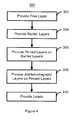
- FIG. 4depicts a high-level flow chart of a method 300 for providing a TMR sensor in accordance with the present invention.
- the free layer 110is provided, via step 302 .
- the free layer 110is preferably made up of approximately twenty to one hundred Angstroms of permalloy.
- the barrier layers 112 and 114are provided, via step 304 .
- the barrier layers 112 and 114are preferably formed of five to twenty Angstroms of aluminum oxide.
- the barrier layers 112 and 114will preferably remain at the edges of the free layer.
- the pinned layers 116 and 118 and the AFM layers 120 and 122are provided, via steps 306 and 308 , respectively.
- the pinned layers 116 and 118are provided on the barrier layers 112 and 114 .
- the pinned layers 116 and 118are preferably between thirty and one hundred Angstroms of a magnetic material having a high spin polarization, such as CoFe or NiFe.
- the AFM layers 120 and 122are provided on the pinned layer 116 and 118 .
- the AFM layer 120 and 122are preferably between fifty and three hundred Angstroms of a material such as PtMn, MnFe or IrMn.
- the leadsare provided, via step 310 , allowing current to be driven to and from the TMR sensor 100 .
- FIG. 5depicts a more detailed flow chart of the method 350 in accordance with the present invention.
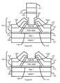
- the method 350will also be described in conjunction with FIGS. 6A through 6G, which depict another embodiment of a TMR sensor 100 ′ during processing.
- the first shieldis provided, via step 352 .
- the first gapis provided on the first shield, via step 354 .
- An optional seed layer for the free layercan then be deposited, via step 356 .
- the seed layeris composed of approximately twenty to fifty Angstroms of Tantalum.
- the material for the free layeris then deposited, via step 358 .
- An optional capping layercan then be provided on the free layer, via step 360 .
- FIG. 6Adepicts the TMR sensor 100 ′ after deposition of the gap 2 a layer, 124 a ′. Also shown are the first shield 102 ′, the first gap 104 ′, the optional seed layer 106 ′, the free layer 110 ′ and the optional capping layer 108 ′.
- Step 364preferably includes providing a bilayer photoresist structure 132 ′, as depicted in FIG. 6 B.
- the gap 2 a layer 124 a ′, the capping layer 108 ′, the free layer 110 ′ and the seed layer 106 ′are then etched using the bilayer photoresist structure 132 ′ as a mask, also in step 364 .
- the width desired for the free layer 110 ′is determined using step 364 .
- These layers 106 ′, 110 ′, 108 ′ and 124 a ′are then ion milled to allow the TMR junctions to be formed at the edges of the free layer 110 ′, via step 366 .
- FIG. 6Cdepicts the TMR sensor 100 ′ after the track width has been defined in step 364 and the free layer has been milled in step 366 .
- FIG. 6Ddepicts the TMR sensor 100 ′ after the insulating layer has been deposited.
- the single insulating layeris shown as being made up of layers 112 ′ and 114 ′ that will be the barrier layers for the TMR sensor 100 ′ and the layer 113 ′ on the bilayer photoresist structure 132 ′.
- a single magnetic layer that will become the pinned layers for the TMR sensor 100 ′is deposited, via step 370 .
- a single AFM layer that will become the AFM layers for the TMR sensor 100 ′is deposited, in step 372 .
- FIG. 6Edepicts the TMR sensor 100 ′ after the steps 370 and 372 have been completed.
- the single magnetic layer that will be used for the pinned layersis indicated by layers 116 ′, 117 ′ and 118 ′.
- the single AFM layer that will be used for the AFM layers of the TMR sensor 100 ′is depicted as layers 120 ′, 121 ′ and 122 ′.
- the portions 113 ′, 117 ′ and 121 ′ of the barrier layer, the magnetic layer and the AFM layer, respectively,are on the bilayer photoresist structure 132 ′.
- FIG. 6Fdepicts the TMR sensor 100 ′ after the lift-off process is performed in step 374 .
- two barrier layers 112 ′ and 114 ′, two pinned layers 116 ′ and 118 ′ and two AFM layers 120 ′ and 122 ′remain.
- TMR junctionsare formed at the edges of the free layer 110 ′.
- a first TMR junctionis formed by an edge of the free layer 110 ′, the first barrier layer 112 ′ and the first pinned layer 116 ′, while a second TMR junction is formed by another edge of the free layer 110 ′, the second barrier layer 114 ′ and the second pinned layer 118 ′.
- the leadsare provided, via step 375 .
- a second portion of the second gaptermed gap 2 b
- the magnetic orientations of the AFM layers 120 ′ and 122 ′are set, via step 378 .
- the magnetic orientations of the AFM layers 120 ′ and 122 ′are set such that the magnetization of the pinned layers 116 ′ and 118 ′, respectively, are perpendicular to the air bearing surface and, preferably, perpendicular to the direction current flows.
- the second shieldis also provided, via step 380 .
- the completed TMR sensor 100 ′, including the gap 2 b 124 b ′ and the second shield 126is depicted in FIG. 6 G.
- the leads to the TMR sensor 100 ′are also depicted in FIG. 6G, however the leads structure of Ta/Au/Ta for GMR heads could also be used to make contact to the free layer 110 ′ in this embodiment.
- the leads or 100 ′has essentially the same benefits as the TMR sensor 100 .
- FIG. 6Hdepicts another embodiment of the TMR sensor 100 ′′.
- the TMR sensor 100 ′′is substantially the same as the TMR sensors 100 and 100 ′. Therefore, the TMR sensor 100 ′′ has substantially the same benefits as the TMR sensors 100 and 100 ′.
- the leads 128 ′′ and 130 ′′are coupled to the outside edge of the TMR sensor 100 ′′, rather than being above the AFM layers 120 ′′ and 122 ′′.
- the leads 128 and 130 , 128 ′ and 130 ′ and 128 ′′ and 130 ′′are depicted as touching the AFM layers 120 and 122 , 120 ′ and 122 ′ and 12 ′′ and 122 ′′ in FIGS.
- the leads 128 and 130 , 128 ′ and 130 ′ and 128 ′′ and 130 ′′are preferably a non-magnetic metal. Furthermore, although the leads 128 and 130 , 128 ′ and 130 ′ and 128 ′′ and 130 ′′ are depicted in FIGS. 2A, 6 G and 6 H are as seen from the air-bearing surface, the leads 128 and 130 , 128 ′ and 130 ′ and 128 ′′ and 130 ′′ need not reach the air-bearing surface.
- the methods 300 and 350 used to provide the TMR sensors 100 and 100 ′are similar to techniques used in forming conventional GMR sensors.
- the methods 300 and 350can be easily integrated into current processing technology.
- the methods 300 and 350can provide a superior TMR sensor 100 or 100 ′ having a more uniform bias current, having a higher signal and that is suitable for use in high areal density recording applications, including for areal densities of one hundred Gb/in 2 .
- the methods 300 and 350are also relatively simple to carry out, facilitating processing of the TMR sensors 100 and 100 ′.
Landscapes
- Engineering & Computer Science (AREA)
- Chemical & Material Sciences (AREA)
- Nanotechnology (AREA)
- Manufacturing & Machinery (AREA)
- Crystallography & Structural Chemistry (AREA)
- Physics & Mathematics (AREA)
- Mathematical Physics (AREA)
- Theoretical Computer Science (AREA)
- Hall/Mr Elements (AREA)
- Measuring Magnetic Variables (AREA)
- Magnetic Heads (AREA)
- Thin Magnetic Films (AREA)
Abstract
Description
Claims (8)
Priority Applications (2)
| Application Number | Priority Date | Filing Date | Title |
|---|---|---|---|
| US09/523,025US6445554B1 (en) | 2000-03-10 | 2000-03-10 | Method and system for providing edge-junction TMR for high areal density magnetic recording |
| JP2001066856AJP2001319313A (en) | 2000-03-10 | 2001-03-09 | Method and device for forming end face junction tmr for high surface density magnetic recording |
Applications Claiming Priority (1)
| Application Number | Priority Date | Filing Date | Title |
|---|---|---|---|
| US09/523,025US6445554B1 (en) | 2000-03-10 | 2000-03-10 | Method and system for providing edge-junction TMR for high areal density magnetic recording |
Publications (1)
| Publication Number | Publication Date |
|---|---|
| US6445554B1true US6445554B1 (en) | 2002-09-03 |
Family
ID=24083370
Family Applications (1)
| Application Number | Title | Priority Date | Filing Date |
|---|---|---|---|
| US09/523,025Expired - LifetimeUS6445554B1 (en) | 2000-03-10 | 2000-03-10 | Method and system for providing edge-junction TMR for high areal density magnetic recording |
Country Status (2)
| Country | Link |
|---|---|
| US (1) | US6445554B1 (en) |
| JP (1) | JP2001319313A (en) |
Cited By (140)
| Publication number | Priority date | Publication date | Assignee | Title |
|---|---|---|---|---|
| US20010014001A1 (en)* | 1999-12-07 | 2001-08-16 | Fujitsu Limited | Magnetoresistance effect magnetic head and magnetic effect reproducing apparatus |
| US20030112564A1 (en)* | 2001-11-27 | 2003-06-19 | Seagate Technology Llc | Magnetoresistive element using an organic nonmagnetic layer |
| US20050041463A1 (en)* | 2003-08-22 | 2005-02-24 | Drewes Joel A. | Mram layer having domain wall traps |
| US20050128651A1 (en)* | 2003-12-16 | 2005-06-16 | Seagate Technology Llc | Spin polarization enhancement artificial magnet |
| US20050243474A1 (en)* | 2004-04-30 | 2005-11-03 | Hitachi Global Storage Technologies | Self-pinned dual CPP sensor exchange pinned at stripe back-end to avoid amplitude flipping |
| US20050243475A1 (en)* | 2004-04-30 | 2005-11-03 | Heim David E | Spin valve sensor having antiferromagnetic (AFM) pinning layer structures formed in the end regions |
| US20050253181A1 (en)* | 2004-05-14 | 2005-11-17 | Nec Electronics Corporation | Semiconductor device |
| US20060234483A1 (en)* | 2005-04-19 | 2006-10-19 | Hitachi Global Storage Technologies Netherlands B.V. | CPP read sensor fabrication using heat resistant photomask |
| CN1305028C (en)* | 2003-11-27 | 2007-03-14 | 株式会社东芝 | Method and apparatus for testing magnetic head with TMR element |
| WO2011115794A3 (en)* | 2010-03-16 | 2012-01-19 | Massachusetts Institute Of Technology | Switching mechanism of magnetic storage cell and logic unit using current induced domain wall motions |
| US8830628B1 (en) | 2009-02-23 | 2014-09-09 | Western Digital (Fremont), Llc | Method and system for providing a perpendicular magnetic recording head |
| US8879207B1 (en) | 2011-12-20 | 2014-11-04 | Western Digital (Fremont), Llc | Method for providing a side shield for a magnetic recording transducer using an air bridge |
| US8883017B1 (en) | 2013-03-12 | 2014-11-11 | Western Digital (Fremont), Llc | Method and system for providing a read transducer having seamless interfaces |
| US8917581B1 (en) | 2013-12-18 | 2014-12-23 | Western Digital Technologies, Inc. | Self-anneal process for a near field transducer and chimney in a hard disk drive assembly |
| US8923102B1 (en) | 2013-07-16 | 2014-12-30 | Western Digital (Fremont), Llc | Optical grating coupling for interferometric waveguides in heat assisted magnetic recording heads |
| US8947985B1 (en) | 2013-07-16 | 2015-02-03 | Western Digital (Fremont), Llc | Heat assisted magnetic recording transducers having a recessed pole |
| US8953422B1 (en) | 2014-06-10 | 2015-02-10 | Western Digital (Fremont), Llc | Near field transducer using dielectric waveguide core with fine ridge feature |
| US8958272B1 (en) | 2014-06-10 | 2015-02-17 | Western Digital (Fremont), Llc | Interfering near field transducer for energy assisted magnetic recording |
| US8971160B1 (en) | 2013-12-19 | 2015-03-03 | Western Digital (Fremont), Llc | Near field transducer with high refractive index pin for heat assisted magnetic recording |
| US8970988B1 (en) | 2013-12-31 | 2015-03-03 | Western Digital (Fremont), Llc | Electric gaps and method for making electric gaps for multiple sensor arrays |
| US8976635B1 (en) | 2014-06-10 | 2015-03-10 | Western Digital (Fremont), Llc | Near field transducer driven by a transverse electric waveguide for energy assisted magnetic recording |
| US8982508B1 (en) | 2011-10-31 | 2015-03-17 | Western Digital (Fremont), Llc | Method for providing a side shield for a magnetic recording transducer |
| US8980109B1 (en) | 2012-12-11 | 2015-03-17 | Western Digital (Fremont), Llc | Method for providing a magnetic recording transducer using a combined main pole and side shield CMP for a wraparound shield scheme |
| US8988812B1 (en) | 2013-11-27 | 2015-03-24 | Western Digital (Fremont), Llc | Multi-sensor array configuration for a two-dimensional magnetic recording (TDMR) operation |
| US8988825B1 (en) | 2014-02-28 | 2015-03-24 | Western Digital (Fremont, LLC | Method for fabricating a magnetic writer having half-side shields |
| US8984740B1 (en) | 2012-11-30 | 2015-03-24 | Western Digital (Fremont), Llc | Process for providing a magnetic recording transducer having a smooth magnetic seed layer |
| US8993217B1 (en) | 2013-04-04 | 2015-03-31 | Western Digital (Fremont), Llc | Double exposure technique for high resolution disk imaging |
| US8995087B1 (en) | 2006-11-29 | 2015-03-31 | Western Digital (Fremont), Llc | Perpendicular magnetic recording write head having a wrap around shield |
| US9001628B1 (en) | 2013-12-16 | 2015-04-07 | Western Digital (Fremont), Llc | Assistant waveguides for evaluating main waveguide coupling efficiency and diode laser alignment tolerances for hard disk |
| US9001467B1 (en) | 2014-03-05 | 2015-04-07 | Western Digital (Fremont), Llc | Method for fabricating side shields in a magnetic writer |
| US8997832B1 (en) | 2010-11-23 | 2015-04-07 | Western Digital (Fremont), Llc | Method of fabricating micrometer scale components |
| US9007879B1 (en) | 2014-06-10 | 2015-04-14 | Western Digital (Fremont), Llc | Interfering near field transducer having a wide metal bar feature for energy assisted magnetic recording |
| US9007725B1 (en) | 2014-10-07 | 2015-04-14 | Western Digital (Fremont), Llc | Sensor with positive coupling between dual ferromagnetic free layer laminates |
| US9007719B1 (en) | 2013-10-23 | 2015-04-14 | Western Digital (Fremont), Llc | Systems and methods for using double mask techniques to achieve very small features |
| US9013836B1 (en) | 2013-04-02 | 2015-04-21 | Western Digital (Fremont), Llc | Method and system for providing an antiferromagnetically coupled return pole |
| US9042057B1 (en) | 2013-01-09 | 2015-05-26 | Western Digital (Fremont), Llc | Methods for providing magnetic storage elements with high magneto-resistance using Heusler alloys |
| US9042208B1 (en) | 2013-03-11 | 2015-05-26 | Western Digital Technologies, Inc. | Disk drive measuring fly height by applying a bias voltage to an electrically insulated write component of a head |
| US9042058B1 (en) | 2013-10-17 | 2015-05-26 | Western Digital Technologies, Inc. | Shield designed for middle shields in a multiple sensor array |
| US9042051B2 (en) | 2013-08-15 | 2015-05-26 | Western Digital (Fremont), Llc | Gradient write gap for perpendicular magnetic recording writer |
| US9042052B1 (en) | 2014-06-23 | 2015-05-26 | Western Digital (Fremont), Llc | Magnetic writer having a partially shunted coil |
| US9053735B1 (en) | 2014-06-20 | 2015-06-09 | Western Digital (Fremont), Llc | Method for fabricating a magnetic writer using a full-film metal planarization |
| US9064528B1 (en) | 2013-05-17 | 2015-06-23 | Western Digital Technologies, Inc. | Interferometric waveguide usable in shingled heat assisted magnetic recording in the absence of a near-field transducer |
| US9064527B1 (en) | 2013-04-12 | 2015-06-23 | Western Digital (Fremont), Llc | High order tapered waveguide for use in a heat assisted magnetic recording head |
| US9065043B1 (en) | 2012-06-29 | 2015-06-23 | Western Digital (Fremont), Llc | Tunnel magnetoresistance read head with narrow shield-to-shield spacing |
| US9064507B1 (en) | 2009-07-31 | 2015-06-23 | Western Digital (Fremont), Llc | Magnetic etch-stop layer for magnetoresistive read heads |
| US9070381B1 (en) | 2013-04-12 | 2015-06-30 | Western Digital (Fremont), Llc | Magnetic recording read transducer having a laminated free layer |
| US9082423B1 (en) | 2013-12-18 | 2015-07-14 | Western Digital (Fremont), Llc | Magnetic recording write transducer having an improved trailing surface profile |
| US9087527B1 (en) | 2014-10-28 | 2015-07-21 | Western Digital (Fremont), Llc | Apparatus and method for middle shield connection in magnetic recording transducers |
| US9087534B1 (en) | 2011-12-20 | 2015-07-21 | Western Digital (Fremont), Llc | Method and system for providing a read transducer having soft and hard magnetic bias structures |
| US9093639B2 (en) | 2012-02-21 | 2015-07-28 | Western Digital (Fremont), Llc | Methods for manufacturing a magnetoresistive structure utilizing heating and cooling |
| US9104107B1 (en) | 2013-04-03 | 2015-08-11 | Western Digital (Fremont), Llc | DUV photoresist process |
| US9111564B1 (en) | 2013-04-02 | 2015-08-18 | Western Digital (Fremont), Llc | Magnetic recording writer having a main pole with multiple flare angles |
| US9111558B1 (en) | 2014-03-14 | 2015-08-18 | Western Digital (Fremont), Llc | System and method of diffractive focusing of light in a waveguide |
| US9111550B1 (en) | 2014-12-04 | 2015-08-18 | Western Digital (Fremont), Llc | Write transducer having a magnetic buffer layer spaced between a side shield and a write pole by non-magnetic layers |
| US9123362B1 (en) | 2011-03-22 | 2015-09-01 | Western Digital (Fremont), Llc | Methods for assembling an electrically assisted magnetic recording (EAMR) head |
| US9123359B1 (en) | 2010-12-22 | 2015-09-01 | Western Digital (Fremont), Llc | Magnetic recording transducer with sputtered antiferromagnetic coupling trilayer between plated ferromagnetic shields and method of fabrication |
| US9123374B1 (en) | 2015-02-12 | 2015-09-01 | Western Digital (Fremont), Llc | Heat assisted magnetic recording writer having an integrated polarization rotation plate |
| US9123358B1 (en) | 2012-06-11 | 2015-09-01 | Western Digital (Fremont), Llc | Conformal high moment side shield seed layer for perpendicular magnetic recording writer |
| US9135937B1 (en) | 2014-05-09 | 2015-09-15 | Western Digital (Fremont), Llc | Current modulation on laser diode for energy assisted magnetic recording transducer |
| US9135930B1 (en) | 2014-03-06 | 2015-09-15 | Western Digital (Fremont), Llc | Method for fabricating a magnetic write pole using vacuum deposition |
| US9142233B1 (en) | 2014-02-28 | 2015-09-22 | Western Digital (Fremont), Llc | Heat assisted magnetic recording writer having a recessed pole |
| US9147408B1 (en) | 2013-12-19 | 2015-09-29 | Western Digital (Fremont), Llc | Heated AFM layer deposition and cooling process for TMR magnetic recording sensor with high pinning field |
| US9147404B1 (en) | 2015-03-31 | 2015-09-29 | Western Digital (Fremont), Llc | Method and system for providing a read transducer having a dual free layer |
| US9153255B1 (en) | 2014-03-05 | 2015-10-06 | Western Digital (Fremont), Llc | Method for fabricating a magnetic writer having an asymmetric gap and shields |
| US9183854B2 (en) | 2014-02-24 | 2015-11-10 | Western Digital (Fremont), Llc | Method to make interferometric taper waveguide for HAMR light delivery |
| US9190079B1 (en) | 2014-09-22 | 2015-11-17 | Western Digital (Fremont), Llc | Magnetic write pole having engineered radius of curvature and chisel angle profiles |
| US9190085B1 (en) | 2014-03-12 | 2015-11-17 | Western Digital (Fremont), Llc | Waveguide with reflective grating for localized energy intensity |
| US9194692B1 (en) | 2013-12-06 | 2015-11-24 | Western Digital (Fremont), Llc | Systems and methods for using white light interferometry to measure undercut of a bi-layer structure |
| US9202493B1 (en) | 2014-02-28 | 2015-12-01 | Western Digital (Fremont), Llc | Method of making an ultra-sharp tip mode converter for a HAMR head |
| US9202480B2 (en) | 2009-10-14 | 2015-12-01 | Western Digital (Fremont), LLC. | Double patterning hard mask for damascene perpendicular magnetic recording (PMR) writer |
| US9214172B2 (en) | 2013-10-23 | 2015-12-15 | Western Digital (Fremont), Llc | Method of manufacturing a magnetic read head |
| US9214169B1 (en) | 2014-06-20 | 2015-12-15 | Western Digital (Fremont), Llc | Magnetic recording read transducer having a laminated free layer |
| US9213322B1 (en) | 2012-08-16 | 2015-12-15 | Western Digital (Fremont), Llc | Methods for providing run to run process control using a dynamic tuner |
| US9214165B1 (en) | 2014-12-18 | 2015-12-15 | Western Digital (Fremont), Llc | Magnetic writer having a gradient in saturation magnetization of the shields |
| US9230565B1 (en) | 2014-06-24 | 2016-01-05 | Western Digital (Fremont), Llc | Magnetic shield for magnetic recording head |
| US9236560B1 (en) | 2014-12-08 | 2016-01-12 | Western Digital (Fremont), Llc | Spin transfer torque tunneling magnetoresistive device having a laminated free layer with perpendicular magnetic anisotropy |
| US9245545B1 (en) | 2013-04-12 | 2016-01-26 | Wester Digital (Fremont), Llc | Short yoke length coils for magnetic heads in disk drives |
| US9245543B1 (en) | 2010-06-25 | 2016-01-26 | Western Digital (Fremont), Llc | Method for providing an energy assisted magnetic recording head having a laser integrally mounted to the slider |
| US9245562B1 (en) | 2015-03-30 | 2016-01-26 | Western Digital (Fremont), Llc | Magnetic recording writer with a composite main pole |
| US9251813B1 (en) | 2009-04-19 | 2016-02-02 | Western Digital (Fremont), Llc | Method of making a magnetic recording head |
| US9263071B1 (en) | 2015-03-31 | 2016-02-16 | Western Digital (Fremont), Llc | Flat NFT for heat assisted magnetic recording |
| US9263067B1 (en) | 2013-05-29 | 2016-02-16 | Western Digital (Fremont), Llc | Process for making PMR writer with constant side wall angle |
| US9269382B1 (en) | 2012-06-29 | 2016-02-23 | Western Digital (Fremont), Llc | Method and system for providing a read transducer having improved pinning of the pinned layer at higher recording densities |
| US9275657B1 (en) | 2013-08-14 | 2016-03-01 | Western Digital (Fremont), Llc | Process for making PMR writer with non-conformal side gaps |
| US9280990B1 (en) | 2013-12-11 | 2016-03-08 | Western Digital (Fremont), Llc | Method for fabricating a magnetic writer using multiple etches |
| US9286919B1 (en) | 2014-12-17 | 2016-03-15 | Western Digital (Fremont), Llc | Magnetic writer having a dual side gap |
| US9287494B1 (en) | 2013-06-28 | 2016-03-15 | Western Digital (Fremont), Llc | Magnetic tunnel junction (MTJ) with a magnesium oxide tunnel barrier |
| US9305583B1 (en) | 2014-02-18 | 2016-04-05 | Western Digital (Fremont), Llc | Method for fabricating a magnetic writer using multiple etches of damascene materials |
| US9312064B1 (en) | 2015-03-02 | 2016-04-12 | Western Digital (Fremont), Llc | Method to fabricate a magnetic head including ion milling of read gap using dual layer hard mask |
| US9318130B1 (en) | 2013-07-02 | 2016-04-19 | Western Digital (Fremont), Llc | Method to fabricate tunneling magnetic recording heads with extended pinned layer |
| US9336814B1 (en) | 2013-03-12 | 2016-05-10 | Western Digital (Fremont), Llc | Inverse tapered waveguide for use in a heat assisted magnetic recording head |
| US9343087B1 (en) | 2014-12-21 | 2016-05-17 | Western Digital (Fremont), Llc | Method for fabricating a magnetic writer having half shields |
| US9343098B1 (en) | 2013-08-23 | 2016-05-17 | Western Digital (Fremont), Llc | Method for providing a heat assisted magnetic recording transducer having protective pads |
| US9343086B1 (en) | 2013-09-11 | 2016-05-17 | Western Digital (Fremont), Llc | Magnetic recording write transducer having an improved sidewall angle profile |
| US9349392B1 (en) | 2012-05-24 | 2016-05-24 | Western Digital (Fremont), Llc | Methods for improving adhesion on dielectric substrates |
| US9349394B1 (en) | 2013-10-18 | 2016-05-24 | Western Digital (Fremont), Llc | Method for fabricating a magnetic writer having a gradient side gap |
| US9361914B1 (en) | 2014-06-18 | 2016-06-07 | Western Digital (Fremont), Llc | Magnetic sensor with thin capping layer |
| US9361913B1 (en) | 2013-06-03 | 2016-06-07 | Western Digital (Fremont), Llc | Recording read heads with a multi-layer AFM layer methods and apparatuses |
| US9368134B1 (en) | 2010-12-16 | 2016-06-14 | Western Digital (Fremont), Llc | Method and system for providing an antiferromagnetically coupled writer |
| US9384765B1 (en) | 2015-09-24 | 2016-07-05 | Western Digital (Fremont), Llc | Method and system for providing a HAMR writer having improved optical efficiency |
| US9384763B1 (en) | 2015-03-26 | 2016-07-05 | Western Digital (Fremont), Llc | Dual free layer magnetic reader having a rear bias structure including a soft bias layer |
| US9396742B1 (en) | 2012-11-30 | 2016-07-19 | Western Digital (Fremont), Llc | Magnetoresistive sensor for a magnetic storage system read head, and fabrication method thereof |
| US9396743B1 (en) | 2014-02-28 | 2016-07-19 | Western Digital (Fremont), Llc | Systems and methods for controlling soft bias thickness for tunnel magnetoresistance readers |
| US9406331B1 (en) | 2013-06-17 | 2016-08-02 | Western Digital (Fremont), Llc | Method for making ultra-narrow read sensor and read transducer device resulting therefrom |
| US9424866B1 (en) | 2015-09-24 | 2016-08-23 | Western Digital (Fremont), Llc | Heat assisted magnetic recording write apparatus having a dielectric gap |
| US9431039B1 (en) | 2013-05-21 | 2016-08-30 | Western Digital (Fremont), Llc | Multiple sensor array usable in two-dimensional magnetic recording |
| US9431031B1 (en) | 2015-03-24 | 2016-08-30 | Western Digital (Fremont), Llc | System and method for magnetic transducers having multiple sensors and AFC shields |
| US9431032B1 (en) | 2013-08-14 | 2016-08-30 | Western Digital (Fremont), Llc | Electrical connection arrangement for a multiple sensor array usable in two-dimensional magnetic recording |
| US9431038B1 (en) | 2015-06-29 | 2016-08-30 | Western Digital (Fremont), Llc | Method for fabricating a magnetic write pole having an improved sidewall angle profile |
| US9431047B1 (en) | 2013-05-01 | 2016-08-30 | Western Digital (Fremont), Llc | Method for providing an improved AFM reader shield |
| US9437251B1 (en) | 2014-12-22 | 2016-09-06 | Western Digital (Fremont), Llc | Apparatus and method having TDMR reader to reader shunts |
| US9441938B1 (en) | 2013-10-08 | 2016-09-13 | Western Digital (Fremont), Llc | Test structures for measuring near field transducer disc length |
| US9443541B1 (en) | 2015-03-24 | 2016-09-13 | Western Digital (Fremont), Llc | Magnetic writer having a gradient in saturation magnetization of the shields and return pole |
| US9449625B1 (en) | 2014-12-24 | 2016-09-20 | Western Digital (Fremont), Llc | Heat assisted magnetic recording head having a plurality of diffusion barrier layers |
| US9449621B1 (en) | 2015-03-26 | 2016-09-20 | Western Digital (Fremont), Llc | Dual free layer magnetic reader having a rear bias structure having a high aspect ratio |
| US9472216B1 (en) | 2015-09-23 | 2016-10-18 | Western Digital (Fremont), Llc | Differential dual free layer magnetic reader |
| US9484051B1 (en) | 2015-11-09 | 2016-11-01 | The Provost, Fellows, Foundation Scholars and the other members of Board, of the College of the Holy and Undivided Trinity of Queen Elizabeth near Dublin | Method and system for reducing undesirable reflections in a HAMR write apparatus |
| US9508363B1 (en) | 2014-06-17 | 2016-11-29 | Western Digital (Fremont), Llc | Method for fabricating a magnetic write pole having a leading edge bevel |
| US9508372B1 (en) | 2015-06-03 | 2016-11-29 | Western Digital (Fremont), Llc | Shingle magnetic writer having a low sidewall angle pole |
| US9508365B1 (en) | 2015-06-24 | 2016-11-29 | Western Digital (Fremont), LLC. | Magnetic reader having a crystal decoupling structure |
| US9530443B1 (en) | 2015-06-25 | 2016-12-27 | Western Digital (Fremont), Llc | Method for fabricating a magnetic recording device having a high aspect ratio structure |
| US9564150B1 (en) | 2015-11-24 | 2017-02-07 | Western Digital (Fremont), Llc | Magnetic read apparatus having an improved read sensor isolation circuit |
| US9595273B1 (en) | 2015-09-30 | 2017-03-14 | Western Digital (Fremont), Llc | Shingle magnetic writer having nonconformal shields |
| US9646639B2 (en) | 2015-06-26 | 2017-05-09 | Western Digital (Fremont), Llc | Heat assisted magnetic recording writer having integrated polarization rotation waveguides |
| US9666214B1 (en) | 2015-09-23 | 2017-05-30 | Western Digital (Fremont), Llc | Free layer magnetic reader that may have a reduced shield-to-shield spacing |
| US9721595B1 (en) | 2014-12-04 | 2017-08-01 | Western Digital (Fremont), Llc | Method for providing a storage device |
| US9740805B1 (en) | 2015-12-01 | 2017-08-22 | Western Digital (Fremont), Llc | Method and system for detecting hotspots for photolithographically-defined devices |
| US9741366B1 (en) | 2014-12-18 | 2017-08-22 | Western Digital (Fremont), Llc | Method for fabricating a magnetic writer having a gradient in saturation magnetization of the shields |
| US9754611B1 (en) | 2015-11-30 | 2017-09-05 | Western Digital (Fremont), Llc | Magnetic recording write apparatus having a stepped conformal trailing shield |
| US9767831B1 (en) | 2015-12-01 | 2017-09-19 | Western Digital (Fremont), Llc | Magnetic writer having convex trailing surface pole and conformal write gap |
| US9786301B1 (en) | 2014-12-02 | 2017-10-10 | Western Digital (Fremont), Llc | Apparatuses and methods for providing thin shields in a multiple sensor array |
| US9799351B1 (en) | 2015-11-30 | 2017-10-24 | Western Digital (Fremont), Llc | Short yoke length writer having assist coils |
| US9812155B1 (en) | 2015-11-23 | 2017-11-07 | Western Digital (Fremont), Llc | Method and system for fabricating high junction angle read sensors |
| US9842615B1 (en) | 2015-06-26 | 2017-12-12 | Western Digital (Fremont), Llc | Magnetic reader having a nonmagnetic insertion layer for the pinning layer |
| US9858951B1 (en) | 2015-12-01 | 2018-01-02 | Western Digital (Fremont), Llc | Method for providing a multilayer AFM layer in a read sensor |
| US9881638B1 (en) | 2014-12-17 | 2018-01-30 | Western Digital (Fremont), Llc | Method for providing a near-field transducer (NFT) for a heat assisted magnetic recording (HAMR) device |
| US9934811B1 (en) | 2014-03-07 | 2018-04-03 | Western Digital (Fremont), Llc | Methods for controlling stray fields of magnetic features using magneto-elastic anisotropy |
| US9953670B1 (en) | 2015-11-10 | 2018-04-24 | Western Digital (Fremont), Llc | Method and system for providing a HAMR writer including a multi-mode interference device |
| US10037770B1 (en) | 2015-11-12 | 2018-07-31 | Western Digital (Fremont), Llc | Method for providing a magnetic recording write apparatus having a seamless pole |
| US10074387B1 (en) | 2014-12-21 | 2018-09-11 | Western Digital (Fremont), Llc | Method and system for providing a read transducer having symmetric antiferromagnetically coupled shields |
Families Citing this family (3)
| Publication number | Priority date | Publication date | Assignee | Title |
|---|---|---|---|---|
| JP2006148039A (en)* | 2004-03-03 | 2006-06-08 | Toshiba Corp | Magnetoresistive element and magnetic memory |
| JP5157891B2 (en)* | 2008-12-26 | 2013-03-06 | 富士通株式会社 | Magnetic detecting element and magnetic reproducing apparatus |
| JP6072478B2 (en)* | 2012-09-07 | 2017-02-01 | 株式会社日立ハイテクノロジーズ | Method for manufacturing magnetoresistive element |
Citations (2)
| Publication number | Priority date | Publication date | Assignee | Title |
|---|---|---|---|---|
| US6178074B1 (en)* | 1998-11-19 | 2001-01-23 | International Business Machines Corporation | Double tunnel junction with magnetoresistance enhancement layer |
| US6185079B1 (en)* | 1998-11-09 | 2001-02-06 | International Business Machines Corporation | Disk drive with thermal asperity reduction circuitry using a magnetic tunnel junction sensor |
- 2000
- 2000-03-10USUS09/523,025patent/US6445554B1/ennot_activeExpired - Lifetime
- 2001
- 2001-03-09JPJP2001066856Apatent/JP2001319313A/enactivePending
Patent Citations (2)
| Publication number | Priority date | Publication date | Assignee | Title |
|---|---|---|---|---|
| US6185079B1 (en)* | 1998-11-09 | 2001-02-06 | International Business Machines Corporation | Disk drive with thermal asperity reduction circuitry using a magnetic tunnel junction sensor |
| US6178074B1 (en)* | 1998-11-19 | 2001-01-23 | International Business Machines Corporation | Double tunnel junction with magnetoresistance enhancement layer |
Cited By (169)
| Publication number | Priority date | Publication date | Assignee | Title |
|---|---|---|---|---|
| US6721147B2 (en)* | 1999-12-07 | 2004-04-13 | Fujitsu Limited | Longitudinally biased magnetoresistance effect magnetic head and magnetic reproducing apparatus |
| US20010014001A1 (en)* | 1999-12-07 | 2001-08-16 | Fujitsu Limited | Magnetoresistance effect magnetic head and magnetic effect reproducing apparatus |
| US20030112564A1 (en)* | 2001-11-27 | 2003-06-19 | Seagate Technology Llc | Magnetoresistive element using an organic nonmagnetic layer |
| US7248446B2 (en) | 2001-11-27 | 2007-07-24 | Seagate Technology Llc | Magnetoresistive element using an organic nonmagnetic layer |
| US7517704B2 (en) | 2003-08-22 | 2009-04-14 | Micron Technology, Inc. | MRAM layer having domain wall traps |
| US20050041463A1 (en)* | 2003-08-22 | 2005-02-24 | Drewes Joel A. | Mram layer having domain wall traps |
| US20070292973A1 (en)* | 2003-08-22 | 2007-12-20 | Micron Technology, Inc. | Mram layer having domain wall traps |
| US7267999B2 (en) | 2003-08-22 | 2007-09-11 | Micron Technology, Inc. | MRAM layer having domain wall traps |
| US7034374B2 (en)* | 2003-08-22 | 2006-04-25 | Micron Technology, Inc. | MRAM layer having domain wall traps |
| US20060108655A1 (en)* | 2003-08-22 | 2006-05-25 | Micron Technology, Inc. | MRAM layer having domain wall traps |
| CN1305028C (en)* | 2003-11-27 | 2007-03-14 | 株式会社东芝 | Method and apparatus for testing magnetic head with TMR element |
| US7099122B2 (en) | 2003-12-16 | 2006-08-29 | Seagate Technology Llc | Spin polarization enhancement artificial magnet |
| US20050128651A1 (en)* | 2003-12-16 | 2005-06-16 | Seagate Technology Llc | Spin polarization enhancement artificial magnet |
| US7324310B2 (en) | 2004-04-30 | 2008-01-29 | Hitachi Global Storage Technologies Netherlands B.V. | Self-pinned dual CPP sensor exchange pinned at stripe back-end to avoid amplitude flipping |
| US20050243475A1 (en)* | 2004-04-30 | 2005-11-03 | Heim David E | Spin valve sensor having antiferromagnetic (AFM) pinning layer structures formed in the end regions |
| US20050243474A1 (en)* | 2004-04-30 | 2005-11-03 | Hitachi Global Storage Technologies | Self-pinned dual CPP sensor exchange pinned at stripe back-end to avoid amplitude flipping |
| US7268981B2 (en) | 2004-04-30 | 2007-09-11 | Hitachi Global Storage Technologies Netherlands B.V. | Spin valve sensor having antiferromagnetic (AFM) pinning layer structures formed in the end regions |
| US20050253181A1 (en)* | 2004-05-14 | 2005-11-17 | Nec Electronics Corporation | Semiconductor device |
| US20060234483A1 (en)* | 2005-04-19 | 2006-10-19 | Hitachi Global Storage Technologies Netherlands B.V. | CPP read sensor fabrication using heat resistant photomask |
| US7530158B2 (en) | 2005-04-19 | 2009-05-12 | Hitachi Global Storage Technologies Netherlands B.V. | CPP read sensor fabrication using heat resistant photomask |
| US8995087B1 (en) | 2006-11-29 | 2015-03-31 | Western Digital (Fremont), Llc | Perpendicular magnetic recording write head having a wrap around shield |
| US8830628B1 (en) | 2009-02-23 | 2014-09-09 | Western Digital (Fremont), Llc | Method and system for providing a perpendicular magnetic recording head |
| US9251813B1 (en) | 2009-04-19 | 2016-02-02 | Western Digital (Fremont), Llc | Method of making a magnetic recording head |
| US9064507B1 (en) | 2009-07-31 | 2015-06-23 | Western Digital (Fremont), Llc | Magnetic etch-stop layer for magnetoresistive read heads |
| US9202480B2 (en) | 2009-10-14 | 2015-12-01 | Western Digital (Fremont), LLC. | Double patterning hard mask for damascene perpendicular magnetic recording (PMR) writer |
| WO2011115794A3 (en)* | 2010-03-16 | 2012-01-19 | Massachusetts Institute Of Technology | Switching mechanism of magnetic storage cell and logic unit using current induced domain wall motions |
| US9245543B1 (en) | 2010-06-25 | 2016-01-26 | Western Digital (Fremont), Llc | Method for providing an energy assisted magnetic recording head having a laser integrally mounted to the slider |
| US9159345B1 (en) | 2010-11-23 | 2015-10-13 | Western Digital (Fremont), Llc | Micrometer scale components |
| US8997832B1 (en) | 2010-11-23 | 2015-04-07 | Western Digital (Fremont), Llc | Method of fabricating micrometer scale components |
| US9672847B2 (en) | 2010-11-23 | 2017-06-06 | Western Digital (Fremont), Llc | Micrometer scale components |
| US9368134B1 (en) | 2010-12-16 | 2016-06-14 | Western Digital (Fremont), Llc | Method and system for providing an antiferromagnetically coupled writer |
| US9123359B1 (en) | 2010-12-22 | 2015-09-01 | Western Digital (Fremont), Llc | Magnetic recording transducer with sputtered antiferromagnetic coupling trilayer between plated ferromagnetic shields and method of fabrication |
| US9123362B1 (en) | 2011-03-22 | 2015-09-01 | Western Digital (Fremont), Llc | Methods for assembling an electrically assisted magnetic recording (EAMR) head |
| US8982508B1 (en) | 2011-10-31 | 2015-03-17 | Western Digital (Fremont), Llc | Method for providing a side shield for a magnetic recording transducer |
| US9087534B1 (en) | 2011-12-20 | 2015-07-21 | Western Digital (Fremont), Llc | Method and system for providing a read transducer having soft and hard magnetic bias structures |
| US8879207B1 (en) | 2011-12-20 | 2014-11-04 | Western Digital (Fremont), Llc | Method for providing a side shield for a magnetic recording transducer using an air bridge |
| US9093639B2 (en) | 2012-02-21 | 2015-07-28 | Western Digital (Fremont), Llc | Methods for manufacturing a magnetoresistive structure utilizing heating and cooling |
| US9940950B2 (en) | 2012-05-24 | 2018-04-10 | Western Digital (Fremont), Llc | Methods for improving adhesion on dielectric substrates |
| US9349392B1 (en) | 2012-05-24 | 2016-05-24 | Western Digital (Fremont), Llc | Methods for improving adhesion on dielectric substrates |
| US9123358B1 (en) | 2012-06-11 | 2015-09-01 | Western Digital (Fremont), Llc | Conformal high moment side shield seed layer for perpendicular magnetic recording writer |
| US9412400B2 (en) | 2012-06-29 | 2016-08-09 | Western Digital (Fremont), Llc | Tunnel magnetoresistance read head with narrow shield-to-shield spacing |
| US9269382B1 (en) | 2012-06-29 | 2016-02-23 | Western Digital (Fremont), Llc | Method and system for providing a read transducer having improved pinning of the pinned layer at higher recording densities |
| US9065043B1 (en) | 2012-06-29 | 2015-06-23 | Western Digital (Fremont), Llc | Tunnel magnetoresistance read head with narrow shield-to-shield spacing |
| US9213322B1 (en) | 2012-08-16 | 2015-12-15 | Western Digital (Fremont), Llc | Methods for providing run to run process control using a dynamic tuner |
| US8984740B1 (en) | 2012-11-30 | 2015-03-24 | Western Digital (Fremont), Llc | Process for providing a magnetic recording transducer having a smooth magnetic seed layer |
| US9396742B1 (en) | 2012-11-30 | 2016-07-19 | Western Digital (Fremont), Llc | Magnetoresistive sensor for a magnetic storage system read head, and fabrication method thereof |
| US8980109B1 (en) | 2012-12-11 | 2015-03-17 | Western Digital (Fremont), Llc | Method for providing a magnetic recording transducer using a combined main pole and side shield CMP for a wraparound shield scheme |
| US9042057B1 (en) | 2013-01-09 | 2015-05-26 | Western Digital (Fremont), Llc | Methods for providing magnetic storage elements with high magneto-resistance using Heusler alloys |
| US9042208B1 (en) | 2013-03-11 | 2015-05-26 | Western Digital Technologies, Inc. | Disk drive measuring fly height by applying a bias voltage to an electrically insulated write component of a head |
| US9336814B1 (en) | 2013-03-12 | 2016-05-10 | Western Digital (Fremont), Llc | Inverse tapered waveguide for use in a heat assisted magnetic recording head |
| US8883017B1 (en) | 2013-03-12 | 2014-11-11 | Western Digital (Fremont), Llc | Method and system for providing a read transducer having seamless interfaces |
| US9013836B1 (en) | 2013-04-02 | 2015-04-21 | Western Digital (Fremont), Llc | Method and system for providing an antiferromagnetically coupled return pole |
| US9111564B1 (en) | 2013-04-02 | 2015-08-18 | Western Digital (Fremont), Llc | Magnetic recording writer having a main pole with multiple flare angles |
| US9104107B1 (en) | 2013-04-03 | 2015-08-11 | Western Digital (Fremont), Llc | DUV photoresist process |
| US8993217B1 (en) | 2013-04-04 | 2015-03-31 | Western Digital (Fremont), Llc | Double exposure technique for high resolution disk imaging |
| US9064527B1 (en) | 2013-04-12 | 2015-06-23 | Western Digital (Fremont), Llc | High order tapered waveguide for use in a heat assisted magnetic recording head |
| US9070381B1 (en) | 2013-04-12 | 2015-06-30 | Western Digital (Fremont), Llc | Magnetic recording read transducer having a laminated free layer |
| US9245545B1 (en) | 2013-04-12 | 2016-01-26 | Wester Digital (Fremont), Llc | Short yoke length coils for magnetic heads in disk drives |
| US9431047B1 (en) | 2013-05-01 | 2016-08-30 | Western Digital (Fremont), Llc | Method for providing an improved AFM reader shield |
| US9064528B1 (en) | 2013-05-17 | 2015-06-23 | Western Digital Technologies, Inc. | Interferometric waveguide usable in shingled heat assisted magnetic recording in the absence of a near-field transducer |
| US9431039B1 (en) | 2013-05-21 | 2016-08-30 | Western Digital (Fremont), Llc | Multiple sensor array usable in two-dimensional magnetic recording |
| US9263067B1 (en) | 2013-05-29 | 2016-02-16 | Western Digital (Fremont), Llc | Process for making PMR writer with constant side wall angle |
| US9361913B1 (en) | 2013-06-03 | 2016-06-07 | Western Digital (Fremont), Llc | Recording read heads with a multi-layer AFM layer methods and apparatuses |
| US9406331B1 (en) | 2013-06-17 | 2016-08-02 | Western Digital (Fremont), Llc | Method for making ultra-narrow read sensor and read transducer device resulting therefrom |
| US9287494B1 (en) | 2013-06-28 | 2016-03-15 | Western Digital (Fremont), Llc | Magnetic tunnel junction (MTJ) with a magnesium oxide tunnel barrier |
| US9318130B1 (en) | 2013-07-02 | 2016-04-19 | Western Digital (Fremont), Llc | Method to fabricate tunneling magnetic recording heads with extended pinned layer |
| US8923102B1 (en) | 2013-07-16 | 2014-12-30 | Western Digital (Fremont), Llc | Optical grating coupling for interferometric waveguides in heat assisted magnetic recording heads |
| US8947985B1 (en) | 2013-07-16 | 2015-02-03 | Western Digital (Fremont), Llc | Heat assisted magnetic recording transducers having a recessed pole |
| US9431032B1 (en) | 2013-08-14 | 2016-08-30 | Western Digital (Fremont), Llc | Electrical connection arrangement for a multiple sensor array usable in two-dimensional magnetic recording |
| US9275657B1 (en) | 2013-08-14 | 2016-03-01 | Western Digital (Fremont), Llc | Process for making PMR writer with non-conformal side gaps |
| US9940951B2 (en)* | 2013-08-14 | 2018-04-10 | Western Digital (Fremont), Llc | PMR writer with non-conformal side gaps |
| US9042051B2 (en) | 2013-08-15 | 2015-05-26 | Western Digital (Fremont), Llc | Gradient write gap for perpendicular magnetic recording writer |
| US9343098B1 (en) | 2013-08-23 | 2016-05-17 | Western Digital (Fremont), Llc | Method for providing a heat assisted magnetic recording transducer having protective pads |
| US9343086B1 (en) | 2013-09-11 | 2016-05-17 | Western Digital (Fremont), Llc | Magnetic recording write transducer having an improved sidewall angle profile |
| US9441938B1 (en) | 2013-10-08 | 2016-09-13 | Western Digital (Fremont), Llc | Test structures for measuring near field transducer disc length |
| US9042058B1 (en) | 2013-10-17 | 2015-05-26 | Western Digital Technologies, Inc. | Shield designed for middle shields in a multiple sensor array |
| US9349394B1 (en) | 2013-10-18 | 2016-05-24 | Western Digital (Fremont), Llc | Method for fabricating a magnetic writer having a gradient side gap |
| US9214172B2 (en) | 2013-10-23 | 2015-12-15 | Western Digital (Fremont), Llc | Method of manufacturing a magnetic read head |
| US9007719B1 (en) | 2013-10-23 | 2015-04-14 | Western Digital (Fremont), Llc | Systems and methods for using double mask techniques to achieve very small features |
| US9830936B2 (en) | 2013-10-23 | 2017-11-28 | Western Digital (Fremont), Llc | Magnetic read head with antiferromagentic layer |
| US8988812B1 (en) | 2013-11-27 | 2015-03-24 | Western Digital (Fremont), Llc | Multi-sensor array configuration for a two-dimensional magnetic recording (TDMR) operation |
| US9194692B1 (en) | 2013-12-06 | 2015-11-24 | Western Digital (Fremont), Llc | Systems and methods for using white light interferometry to measure undercut of a bi-layer structure |
| US9280990B1 (en) | 2013-12-11 | 2016-03-08 | Western Digital (Fremont), Llc | Method for fabricating a magnetic writer using multiple etches |
| US9001628B1 (en) | 2013-12-16 | 2015-04-07 | Western Digital (Fremont), Llc | Assistant waveguides for evaluating main waveguide coupling efficiency and diode laser alignment tolerances for hard disk |
| US9082423B1 (en) | 2013-12-18 | 2015-07-14 | Western Digital (Fremont), Llc | Magnetic recording write transducer having an improved trailing surface profile |
| US8917581B1 (en) | 2013-12-18 | 2014-12-23 | Western Digital Technologies, Inc. | Self-anneal process for a near field transducer and chimney in a hard disk drive assembly |
| US9147408B1 (en) | 2013-12-19 | 2015-09-29 | Western Digital (Fremont), Llc | Heated AFM layer deposition and cooling process for TMR magnetic recording sensor with high pinning field |
| US8971160B1 (en) | 2013-12-19 | 2015-03-03 | Western Digital (Fremont), Llc | Near field transducer with high refractive index pin for heat assisted magnetic recording |
| US8970988B1 (en) | 2013-12-31 | 2015-03-03 | Western Digital (Fremont), Llc | Electric gaps and method for making electric gaps for multiple sensor arrays |
| US9305583B1 (en) | 2014-02-18 | 2016-04-05 | Western Digital (Fremont), Llc | Method for fabricating a magnetic writer using multiple etches of damascene materials |
| US9183854B2 (en) | 2014-02-24 | 2015-11-10 | Western Digital (Fremont), Llc | Method to make interferometric taper waveguide for HAMR light delivery |
| US8988825B1 (en) | 2014-02-28 | 2015-03-24 | Western Digital (Fremont, LLC | Method for fabricating a magnetic writer having half-side shields |
| US9142233B1 (en) | 2014-02-28 | 2015-09-22 | Western Digital (Fremont), Llc | Heat assisted magnetic recording writer having a recessed pole |
| US9396743B1 (en) | 2014-02-28 | 2016-07-19 | Western Digital (Fremont), Llc | Systems and methods for controlling soft bias thickness for tunnel magnetoresistance readers |
| US9202493B1 (en) | 2014-02-28 | 2015-12-01 | Western Digital (Fremont), Llc | Method of making an ultra-sharp tip mode converter for a HAMR head |
| US9153255B1 (en) | 2014-03-05 | 2015-10-06 | Western Digital (Fremont), Llc | Method for fabricating a magnetic writer having an asymmetric gap and shields |
| US9349393B2 (en) | 2014-03-05 | 2016-05-24 | Western Digital (Fremont), Llc | Magnetic writer having an asymmetric gap and shields |
| US9001467B1 (en) | 2014-03-05 | 2015-04-07 | Western Digital (Fremont), Llc | Method for fabricating side shields in a magnetic writer |
| US9135930B1 (en) | 2014-03-06 | 2015-09-15 | Western Digital (Fremont), Llc | Method for fabricating a magnetic write pole using vacuum deposition |
| US9934811B1 (en) | 2014-03-07 | 2018-04-03 | Western Digital (Fremont), Llc | Methods for controlling stray fields of magnetic features using magneto-elastic anisotropy |
| US9495984B2 (en) | 2014-03-12 | 2016-11-15 | Western Digital (Fremont), Llc | Waveguide with reflective grating for localized energy intensity |
| US9190085B1 (en) | 2014-03-12 | 2015-11-17 | Western Digital (Fremont), Llc | Waveguide with reflective grating for localized energy intensity |
| US9111558B1 (en) | 2014-03-14 | 2015-08-18 | Western Digital (Fremont), Llc | System and method of diffractive focusing of light in a waveguide |
| US9135937B1 (en) | 2014-05-09 | 2015-09-15 | Western Digital (Fremont), Llc | Current modulation on laser diode for energy assisted magnetic recording transducer |
| US8958272B1 (en) | 2014-06-10 | 2015-02-17 | Western Digital (Fremont), Llc | Interfering near field transducer for energy assisted magnetic recording |
| US9311952B2 (en) | 2014-06-10 | 2016-04-12 | Western Digital (Fremont), Llc | Interfering near field transducer for energy assisted magnetic recording |
| US8976635B1 (en) | 2014-06-10 | 2015-03-10 | Western Digital (Fremont), Llc | Near field transducer driven by a transverse electric waveguide for energy assisted magnetic recording |
| US8953422B1 (en) | 2014-06-10 | 2015-02-10 | Western Digital (Fremont), Llc | Near field transducer using dielectric waveguide core with fine ridge feature |
| US9159346B1 (en) | 2014-06-10 | 2015-10-13 | Western Digital (Fremont), Llc | Near field transducer using dielectric waveguide core with fine ridge feature |
| US9007879B1 (en) | 2014-06-10 | 2015-04-14 | Western Digital (Fremont), Llc | Interfering near field transducer having a wide metal bar feature for energy assisted magnetic recording |
| US9508363B1 (en) | 2014-06-17 | 2016-11-29 | Western Digital (Fremont), Llc | Method for fabricating a magnetic write pole having a leading edge bevel |
| US9361914B1 (en) | 2014-06-18 | 2016-06-07 | Western Digital (Fremont), Llc | Magnetic sensor with thin capping layer |
| US9053735B1 (en) | 2014-06-20 | 2015-06-09 | Western Digital (Fremont), Llc | Method for fabricating a magnetic writer using a full-film metal planarization |
| US9214169B1 (en) | 2014-06-20 | 2015-12-15 | Western Digital (Fremont), Llc | Magnetic recording read transducer having a laminated free layer |
| US9042052B1 (en) | 2014-06-23 | 2015-05-26 | Western Digital (Fremont), Llc | Magnetic writer having a partially shunted coil |
| US9230565B1 (en) | 2014-06-24 | 2016-01-05 | Western Digital (Fremont), Llc | Magnetic shield for magnetic recording head |
| US9190079B1 (en) | 2014-09-22 | 2015-11-17 | Western Digital (Fremont), Llc | Magnetic write pole having engineered radius of curvature and chisel angle profiles |
| US9007725B1 (en) | 2014-10-07 | 2015-04-14 | Western Digital (Fremont), Llc | Sensor with positive coupling between dual ferromagnetic free layer laminates |
| US9087527B1 (en) | 2014-10-28 | 2015-07-21 | Western Digital (Fremont), Llc | Apparatus and method for middle shield connection in magnetic recording transducers |
| US9786301B1 (en) | 2014-12-02 | 2017-10-10 | Western Digital (Fremont), Llc | Apparatuses and methods for providing thin shields in a multiple sensor array |
| US9111550B1 (en) | 2014-12-04 | 2015-08-18 | Western Digital (Fremont), Llc | Write transducer having a magnetic buffer layer spaced between a side shield and a write pole by non-magnetic layers |
| US9721595B1 (en) | 2014-12-04 | 2017-08-01 | Western Digital (Fremont), Llc | Method for providing a storage device |
| US9236560B1 (en) | 2014-12-08 | 2016-01-12 | Western Digital (Fremont), Llc | Spin transfer torque tunneling magnetoresistive device having a laminated free layer with perpendicular magnetic anisotropy |
| US9705072B2 (en) | 2014-12-08 | 2017-07-11 | Western Digital (Fremont), Llc | Spin transfer torque tunneling magnetoresistive device having a laminated free layer with perpendicular magnetic anisotropy |
| US10553241B2 (en) | 2014-12-17 | 2020-02-04 | Western Digital Technologies, Inc. | Near-field transducer (NFT) for a heat assisted magnetic recording (HAMR) device |
| US9881638B1 (en) | 2014-12-17 | 2018-01-30 | Western Digital (Fremont), Llc | Method for providing a near-field transducer (NFT) for a heat assisted magnetic recording (HAMR) device |
| US9286919B1 (en) | 2014-12-17 | 2016-03-15 | Western Digital (Fremont), Llc | Magnetic writer having a dual side gap |
| US9214165B1 (en) | 2014-12-18 | 2015-12-15 | Western Digital (Fremont), Llc | Magnetic writer having a gradient in saturation magnetization of the shields |
| US9741366B1 (en) | 2014-12-18 | 2017-08-22 | Western Digital (Fremont), Llc | Method for fabricating a magnetic writer having a gradient in saturation magnetization of the shields |
| US10074387B1 (en) | 2014-12-21 | 2018-09-11 | Western Digital (Fremont), Llc | Method and system for providing a read transducer having symmetric antiferromagnetically coupled shields |
| US9343087B1 (en) | 2014-12-21 | 2016-05-17 | Western Digital (Fremont), Llc | Method for fabricating a magnetic writer having half shields |
| US9437251B1 (en) | 2014-12-22 | 2016-09-06 | Western Digital (Fremont), Llc | Apparatus and method having TDMR reader to reader shunts |
| US9449625B1 (en) | 2014-12-24 | 2016-09-20 | Western Digital (Fremont), Llc | Heat assisted magnetic recording head having a plurality of diffusion barrier layers |
| US9123374B1 (en) | 2015-02-12 | 2015-09-01 | Western Digital (Fremont), Llc | Heat assisted magnetic recording writer having an integrated polarization rotation plate |
| US9312064B1 (en) | 2015-03-02 | 2016-04-12 | Western Digital (Fremont), Llc | Method to fabricate a magnetic head including ion milling of read gap using dual layer hard mask |
| US9443541B1 (en) | 2015-03-24 | 2016-09-13 | Western Digital (Fremont), Llc | Magnetic writer having a gradient in saturation magnetization of the shields and return pole |
| US9431031B1 (en) | 2015-03-24 | 2016-08-30 | Western Digital (Fremont), Llc | System and method for magnetic transducers having multiple sensors and AFC shields |
| US9922672B1 (en) | 2015-03-26 | 2018-03-20 | Western Digital (Fremont), Llc | Dual free layer magnetic reader having a rear bias structure having a high aspect ratio |
| US9449621B1 (en) | 2015-03-26 | 2016-09-20 | Western Digital (Fremont), Llc | Dual free layer magnetic reader having a rear bias structure having a high aspect ratio |
| US9384763B1 (en) | 2015-03-26 | 2016-07-05 | Western Digital (Fremont), Llc | Dual free layer magnetic reader having a rear bias structure including a soft bias layer |
| US9245562B1 (en) | 2015-03-30 | 2016-01-26 | Western Digital (Fremont), Llc | Magnetic recording writer with a composite main pole |
| US9147404B1 (en) | 2015-03-31 | 2015-09-29 | Western Digital (Fremont), Llc | Method and system for providing a read transducer having a dual free layer |
| US9263071B1 (en) | 2015-03-31 | 2016-02-16 | Western Digital (Fremont), Llc | Flat NFT for heat assisted magnetic recording |
| US9508372B1 (en) | 2015-06-03 | 2016-11-29 | Western Digital (Fremont), Llc | Shingle magnetic writer having a low sidewall angle pole |
| US9508365B1 (en) | 2015-06-24 | 2016-11-29 | Western Digital (Fremont), LLC. | Magnetic reader having a crystal decoupling structure |
| US9530443B1 (en) | 2015-06-25 | 2016-12-27 | Western Digital (Fremont), Llc | Method for fabricating a magnetic recording device having a high aspect ratio structure |
| US9842615B1 (en) | 2015-06-26 | 2017-12-12 | Western Digital (Fremont), Llc | Magnetic reader having a nonmagnetic insertion layer for the pinning layer |
| US9646639B2 (en) | 2015-06-26 | 2017-05-09 | Western Digital (Fremont), Llc | Heat assisted magnetic recording writer having integrated polarization rotation waveguides |
| US10037773B2 (en) | 2015-06-26 | 2018-07-31 | Western Digital (Fremont), Llc | Heat assisted magnetic recording writer having integrated polarization rotation waveguides |
| US10242700B2 (en) | 2015-06-26 | 2019-03-26 | Western Digital (Fremont), Llc | Magnetic reader having a nonmagnetic insertion layer for the pinning layer |
| US9431038B1 (en) | 2015-06-29 | 2016-08-30 | Western Digital (Fremont), Llc | Method for fabricating a magnetic write pole having an improved sidewall angle profile |
| US9472216B1 (en) | 2015-09-23 | 2016-10-18 | Western Digital (Fremont), Llc | Differential dual free layer magnetic reader |
| US9666214B1 (en) | 2015-09-23 | 2017-05-30 | Western Digital (Fremont), Llc | Free layer magnetic reader that may have a reduced shield-to-shield spacing |
| US9424866B1 (en) | 2015-09-24 | 2016-08-23 | Western Digital (Fremont), Llc | Heat assisted magnetic recording write apparatus having a dielectric gap |
| US9384765B1 (en) | 2015-09-24 | 2016-07-05 | Western Digital (Fremont), Llc | Method and system for providing a HAMR writer having improved optical efficiency |
| US9595273B1 (en) | 2015-09-30 | 2017-03-14 | Western Digital (Fremont), Llc | Shingle magnetic writer having nonconformal shields |
| US9484051B1 (en) | 2015-11-09 | 2016-11-01 | The Provost, Fellows, Foundation Scholars and the other members of Board, of the College of the Holy and Undivided Trinity of Queen Elizabeth near Dublin | Method and system for reducing undesirable reflections in a HAMR write apparatus |
| US10381029B2 (en) | 2015-11-10 | 2019-08-13 | Western Digital (Fremont), Llc | Method and system for providing a HAMR writer including a multi-mode interference device |
| US9953670B1 (en) | 2015-11-10 | 2018-04-24 | Western Digital (Fremont), Llc | Method and system for providing a HAMR writer including a multi-mode interference device |
| US10037770B1 (en) | 2015-11-12 | 2018-07-31 | Western Digital (Fremont), Llc | Method for providing a magnetic recording write apparatus having a seamless pole |
| US9812155B1 (en) | 2015-11-23 | 2017-11-07 | Western Digital (Fremont), Llc | Method and system for fabricating high junction angle read sensors |
| US9564150B1 (en) | 2015-11-24 | 2017-02-07 | Western Digital (Fremont), Llc | Magnetic read apparatus having an improved read sensor isolation circuit |
| US9799351B1 (en) | 2015-11-30 | 2017-10-24 | Western Digital (Fremont), Llc | Short yoke length writer having assist coils |
| US10121495B2 (en) | 2015-11-30 | 2018-11-06 | Western Digital (Fremont), Llc | Magnetic recording write apparatus having a stepped conformal trailing shield |
| US9754611B1 (en) | 2015-11-30 | 2017-09-05 | Western Digital (Fremont), Llc | Magnetic recording write apparatus having a stepped conformal trailing shield |
| US9767831B1 (en) | 2015-12-01 | 2017-09-19 | Western Digital (Fremont), Llc | Magnetic writer having convex trailing surface pole and conformal write gap |
| US9997177B2 (en) | 2015-12-01 | 2018-06-12 | Western Digital (Fremont), Llc | Magnetic writer having convex trailing surface pole and conformal write gap |
| US9858951B1 (en) | 2015-12-01 | 2018-01-02 | Western Digital (Fremont), Llc | Method for providing a multilayer AFM layer in a read sensor |
| US9740805B1 (en) | 2015-12-01 | 2017-08-22 | Western Digital (Fremont), Llc | Method and system for detecting hotspots for photolithographically-defined devices |
Also Published As
| Publication number | Publication date |
|---|---|
| JP2001319313A (en) | 2001-11-16 |
Similar Documents
| Publication | Publication Date | Title |
|---|---|---|
| US6445554B1 (en) | Method and system for providing edge-junction TMR for high areal density magnetic recording | |
| US6515573B1 (en) | Method and system for providing edge-junction TMR utilizing a hard magnet as a pinned layer | |
| US6512661B1 (en) | Vertical giant magnetoresistance sensor utilizing an insulating bias layer | |
| US11222656B1 (en) | Method to reduce baseline shift for a SOT differential reader | |
| US6456465B1 (en) | Vertical giant magnetoresistance sensor using a recessed shield | |
| US6519124B1 (en) | Magnetic tunnel junction read head using a hybrid, low-magnetization flux guide | |
| US8077435B1 (en) | Current perpendicular-to-plane read sensor with back shield | |
| US8576518B1 (en) | Current-perpendicular-to-the-plane (CPP) magnetoresistive (MR) sensor with exchange-coupled side shield structure | |
| US6833982B2 (en) | Magnetic tunnel junction sensor with a free layer biased by longitudinal layers interfacing top surfaces of free layer extensions which extend beyond an active region of the sensor | |
| US7283333B2 (en) | Self-pinned double tunnel junction head | |
| US6700760B1 (en) | Tunneling magnetoresistive head in current perpendicular to plane mode | |
| US6201673B1 (en) | System for biasing a synthetic free layer in a magnetoresistance sensor | |
| US6473275B1 (en) | Dual hybrid magnetic tunnel junction/giant magnetoresistive sensor | |
| US6947264B2 (en) | Self-pinned in-stack bias structure for magnetoresistive read heads | |
| US6934133B2 (en) | Three terminal magnetic head having a magnetic semiconductor and a tunnel magnetoresistive film and magnetic recording apparatus including the head | |
| US20090080125A1 (en) | Magnetic head | |
| US7573675B2 (en) | Thin film magnetic head | |
| US7639459B2 (en) | Three terminal magnetic sensor having an in-stack longitudinal biasing layer structure | |
| US20160005428A1 (en) | Graded side shield gap reader | |
| CN1538386A (en) | Magnetoresistive Sensors with Antiparallel Coupled Lead/Sensor Overlap | |
| US6426853B1 (en) | Magnetoresistive effect sensor, thin-film magnetic head and thin-film wafer with the thin-film magnetic heads | |
| US20020163767A1 (en) | Magnetoresistive sensor and a thin film magnetic head | |
| US7057865B1 (en) | High sensitivity tunneling GMR sensors with synthetic antiferromagnet free layer | |
| US7426096B2 (en) | Magnetoresistive effective element with high output stability and reduced read bleeding at track edges | |
| US7259942B2 (en) | Three terminal magnetic sensor having an in-stack longitudinal biasing layer structure in the collector or emitter region |
Legal Events
| Date | Code | Title | Description |
|---|---|---|---|
| AS | Assignment | Owner name:READ-RITE CORPORATION, CALIFORNIA Free format text:ASSIGNMENT OF ASSIGNORS INTEREST;ASSIGNORS:DONG, ZI-WENG;SHI, ZHUPEI;REEL/FRAME:010619/0161 Effective date:20000306 | |
| STCF | Information on status: patent grant | Free format text:PATENTED CASE | |
| AS | Assignment | Owner name:TENNENBAUM CAPITAL PARTNERS, LLC, CALIFORNIA Free format text:SECURITY INTEREST;ASSIGNOR:READ-RITE CORPORATION;REEL/FRAME:013616/0399 Effective date:20021224 | |
| AS | Assignment | Owner name:WESTERN DIGITAL (FREMONT), INC., CALIFORNIA Free format text:ASSIGNMENT OF ASSIGNORS INTEREST;ASSIGNOR:READ-RITE CORPORATION;REEL/FRAME:014506/0765 Effective date:20030731 | |
| AS | Assignment | Owner name:READ-RITE CORPORATION, CALIFORNIA Free format text:RELEASE OF SECURITY INTEREST;ASSIGNOR:TENNENBAUM CAPITAL PARTNERS, LLC;REEL/FRAME:014499/0476 Effective date:20030731 | |
| AS | Assignment | Owner name:GENERAL ELECTRIC CAPITAL CORPORATION, AS AGENT, CA Free format text:SECURITY INTEREST;ASSIGNORS:WESTERN DIGITAL TECHNOLOGIES, INC.;WESTERN DIGITAL (FREMONT), INC.;REEL/FRAME:014830/0957 Effective date:20030919 | |
| FPAY | Fee payment | Year of fee payment:4 | |
| AS | Assignment | Owner name:WESTERN DIGITAL (FREMONT), INC., CALIFORNIA Free format text:RELEASE BY SECURED PARTY;ASSIGNOR:GENERAL ELECTRIC CAPITAL CORPORATION, AS AGENT;REEL/FRAME:020599/0489 Effective date:20070809 Owner name:WESTERN DIGITAL TECHNOLOGIES, INC., CALIFORNIA Free format text:RELEASE BY SECURED PARTY;ASSIGNOR:GENERAL ELECTRIC CAPITAL CORPORATION, AS AGENT;REEL/FRAME:020599/0489 Effective date:20070809 | |
| FPAY | Fee payment | Year of fee payment:8 | |
| REMI | Maintenance fee reminder mailed | ||
| FPAY | Fee payment | Year of fee payment:12 | |
| SULP | Surcharge for late payment | Year of fee payment:11 | |
| AS | Assignment | Owner name:JPMORGAN CHASE BANK, N.A., AS COLLATERAL AGENT, IL Free format text:SECURITY AGREEMENT;ASSIGNOR:WESTERN DIGITAL (FREMONT), LLC;REEL/FRAME:038710/0845 Effective date:20160512 Owner name:U.S. BANK NATIONAL ASSOCIATION, AS COLLATERAL AGEN Free format text:SECURITY AGREEMENT;ASSIGNOR:WESTERN DIGITAL (FREMONT), LLC;REEL/FRAME:038744/0675 Effective date:20160512 Owner name:JPMORGAN CHASE BANK, N.A., AS COLLATERAL AGENT, IL Free format text:SECURITY AGREEMENT;ASSIGNOR:WESTERN DIGITAL (FREMONT), LLC;REEL/FRAME:038744/0755 Effective date:20160512 | |
| AS | Assignment | Owner name:WESTERN DIGITAL (FREMONT), LLC, CALIFORNIA Free format text:RELEASE BY SECURED PARTY;ASSIGNOR:U.S. BANK NATIONAL ASSOCIATION, AS COLLATERAL AGENT;REEL/FRAME:045501/0158 Effective date:20180227 | |
| AS | Assignment | Owner name:WESTERN DIGITAL (FREMONT), LLC, CALIFORNIA Free format text:ENTITY CONVERSION FROM INC TO LLC;ASSIGNOR:WESTERN DIGITAL (FREMONT), INC;REEL/FRAME:048501/0925 Effective date:20070629 | |
| AS | Assignment | Owner name:WESTERN DIGITAL TECHNOLOGIES, INC., CALIFORNIA Free format text:ASSIGNMENT OF ASSIGNORS INTEREST;ASSIGNOR:WESTERN DIGITAL (FREMONT), LLC;REEL/FRAME:050450/0582 Effective date:20190508 | |
| AS | Assignment | Owner name:WESTERN DIGITAL TECHNOLOGIES, INC., CALIFORNIA Free format text:RELEASE OF SECURITY INTEREST AT REEL 038710 FRAME 0845;ASSIGNOR:JPMORGAN CHASE BANK, N.A.;REEL/FRAME:058965/0445 Effective date:20220203 Owner name:WESTERN DIGITAL (FREMONT), LLC, CALIFORNIA Free format text:RELEASE OF SECURITY INTEREST AT REEL 038710 FRAME 0845;ASSIGNOR:JPMORGAN CHASE BANK, N.A.;REEL/FRAME:058965/0445 Effective date:20220203 |