US6445536B1 - Dielectric stencil-defined write head for MR, GMR, and spin valve high density recording heads - Google Patents
Dielectric stencil-defined write head for MR, GMR, and spin valve high density recording headsDownload PDFInfo
- Publication number
- US6445536B1 US6445536B1US09/140,903US14090398AUS6445536B1US 6445536 B1US6445536 B1US 6445536B1US 14090398 AUS14090398 AUS 14090398AUS 6445536 B1US6445536 B1US 6445536B1
- Authority
- US
- United States
- Prior art keywords
- thin film
- hbsat
- layer
- film head
- dielectric layer
- Prior art date
- Legal status (The legal status is an assumption and is not a legal conclusion. Google has not performed a legal analysis and makes no representation as to the accuracy of the status listed.)
- Expired - Fee Related
Links
Images


Classifications
- G—PHYSICS
- G11—INFORMATION STORAGE
- G11B—INFORMATION STORAGE BASED ON RELATIVE MOVEMENT BETWEEN RECORD CARRIER AND TRANSDUCER
- G11B5/00—Recording by magnetisation or demagnetisation of a record carrier; Reproducing by magnetic means; Record carriers therefor
- G11B5/127—Structure or manufacture of heads, e.g. inductive
- G11B5/31—Structure or manufacture of heads, e.g. inductive using thin films
- G11B5/3163—Fabrication methods or processes specially adapted for a particular head structure, e.g. using base layers for electroplating, using functional layers for masking, using energy or particle beams for shaping the structure or modifying the properties of the basic layers
- G—PHYSICS
- G11—INFORMATION STORAGE
- G11B—INFORMATION STORAGE BASED ON RELATIVE MOVEMENT BETWEEN RECORD CARRIER AND TRANSDUCER
- G11B5/00—Recording by magnetisation or demagnetisation of a record carrier; Reproducing by magnetic means; Record carriers therefor
- G11B5/127—Structure or manufacture of heads, e.g. inductive
- G11B5/31—Structure or manufacture of heads, e.g. inductive using thin films
- G11B5/3109—Details
- G11B5/3116—Shaping of layers, poles or gaps for improving the form of the electrical signal transduced, e.g. for shielding, contour effect, equalizing, side flux fringing, cross talk reduction between heads or between heads and information tracks
- G—PHYSICS
- G11—INFORMATION STORAGE
- G11B—INFORMATION STORAGE BASED ON RELATIVE MOVEMENT BETWEEN RECORD CARRIER AND TRANSDUCER
- G11B5/00—Recording by magnetisation or demagnetisation of a record carrier; Reproducing by magnetic means; Record carriers therefor
- G11B5/127—Structure or manufacture of heads, e.g. inductive
- G11B5/31—Structure or manufacture of heads, e.g. inductive using thin films
- G11B5/3109—Details
- G11B5/313—Disposition of layers
- G—PHYSICS
- G11—INFORMATION STORAGE
- G11B—INFORMATION STORAGE BASED ON RELATIVE MOVEMENT BETWEEN RECORD CARRIER AND TRANSDUCER
- G11B5/00—Recording by magnetisation or demagnetisation of a record carrier; Reproducing by magnetic means; Record carriers therefor
- G11B5/127—Structure or manufacture of heads, e.g. inductive
- G11B5/33—Structure or manufacture of flux-sensitive heads, i.e. for reproduction only; Combination of such heads with means for recording or erasing only
- G11B5/39—Structure or manufacture of flux-sensitive heads, i.e. for reproduction only; Combination of such heads with means for recording or erasing only using magneto-resistive devices or effects
- G11B5/3903—Structure or manufacture of flux-sensitive heads, i.e. for reproduction only; Combination of such heads with means for recording or erasing only using magneto-resistive devices or effects using magnetic thin film layers or their effects, the films being part of integrated structures
- G11B5/3967—Composite structural arrangements of transducers, e.g. inductive write and magnetoresistive read
Definitions
- the present inventionrelates to thin film magnetic structures.
- the present inventionpertains to a thin film inductive write head.
- the sacrificial layeris removed only to the upper surface of an initial P 2 pole layer, and a key feature of the claimed structure is the substantially equal width of the P 1 and P 2 poles at the write gap in conjunction with a substantially vertical profile of each.
- a key feature of the claimed structureis the substantially equal width of the P 1 and P 2 poles at the write gap in conjunction with a substantially vertical profile of each.
- U.S. Pat. No. 5,285,340 to Ju et al.recites the use of a chemical etching process to produce a cavity on a patternable dielectric material. This cavity is substantially filled by electroplating a first pole layer, a non-magnetic write gap, and a second pole layer. A final P 2 element is stitched in to the remaining cavity to complete the transducer.
- a key feature of the claimsis the substantially equal width of the P 1 and P 2 poles at the write gap in conjunction with a substantially vertical profile of each.
- Write gap thicknessis typically in the range of 1000-5000 angstroms and it is desirable to control this to a tolerance of approximately 200 angstroms or better. Measurement and control of a plated write gap in such an approach can complicate the process requirements for the device or limit the range of the application of this technique as such tight control of thin plated layers can be difficult.
- U.S. Pat. No. 4,947,541 to Toyoda et al.recites a method for producing a thin film head.
- the thin film head formation processes of the Toyoda et al. referenceutilize conventional core formation materials.
- the Toyoda et al. referenceexplicitly recites using conventional permalloy (NiFe) to form the upper and lower cores of a thin film head.
- the Toyoda et al. referencerecites forming the upper core of the thin film head using conventional electroplating techniques.
- HBsat materialsare ideally suited for forming the upper and lower cores of a thin film inductive head.
- most HBsat materialscannot be formed into upper or lower cores using typical fabrication methods.
- many HBsat materialshave physical characteristics rendering them unsuited for electroplating processes.
- such HBsat materialscould not be effectively used, in the manner recited in the Toyoda et al. reference, to form the upper core of a thin film inductive head.
- a needhas arisen for a thin film head formation method which is not limited to use only with conventional core formation materials.
- the present inventionprovides a thin film head formation method which is not limited to use only with conventional core formation materials.
- the present inventionfurther provides a thin film head and a thin film head formation method which utilize advantageous HBsat materials.
- the present inventionalso provides a thin film head formation method which utilizes advantageous HBsat materials but which does not suffer from increased magnetostriction associated with conventional HBsat materials.
- the present inventionrecites forming a cavity in a dielectric layer.
- a layer of high magnetic field saturation (HBsat) materialis sputter-deposited over the dielectric layer such that the HBsat material is deposited into the cavity formed in the dielectric layer.
- the cavity in the dielectric layerfunctions as a mold or “stencil” for the HBsat material.
- the HBsat material deposited into the cavityis used to form the first core of a thin film head.
- a gap layer of materialis deposited above the dielectric layer and above the first core.
- a layer of HBsat materialis sputter-deposited above the gap layer of material and above the first core of the thin film head.
- the layer of HBsat material sputter-deposited above the gap layer of material and above the first coreis used to form the second core of the thin film head.
- this inventionforms first and second cores of a thin film head using sputter-deposition processes.
- selected HBsat materialswhich were not well suited to conventional thin film head formation methods can now be used to form the cores of thin film head structures.
- the present inventionspecifically recites the formation of the above-mentioned cavity in the dielectric layer.
- the present inventionfirst surrounds a sacrificial metal structure with the above-mentioned dielectric layer.
- the present embodimentremoves the sacrificial metal structure. In so doing, an opening remains in the dielectric layer. In this embodiment, the opening defines the cavity in the dielectric layer.
- FIGS. 1A, 1 B, 1 C, 1 D, 1 E, IF, 1 G, 1 H, 1 I, 1 J, 1 K, 1 L, 1 M, 1 N, and 1 Oare side sectional views illustrating process steps employed during the fabrication of a stencil-defined thin film magnetic structure in accordance with the present claimed invention.
- FIGS. 2A, 2 B, 2 C, 2 D, 2 E, 2 F, 2 G, 2 H, 2 I, 2 J, and 2 Kare side sectional views illustrating process steps employed during the fabrication of a stencil-defined thin film magnetic structure in accordance with another embodiment of the present claimed invention.
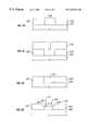
- FIGS. 1A-1Oside sectional views illustrating process steps employed during the fabrication of a stencil-defined thin film magnetic structure in accordance with the present claimed invention are shown.
- layer 100comprises a shield 2 layer of a thin film head.
- layer 100is comprised, for example, of permalloy and has a thickness of approximately 1-3 microns.
- buffer layer 102above layer 100 .
- buffer layeris comprised, for example, of approximately 100-1000 angstroms of a suitable material such as tantalum, chromium, and the like.
- the present embodimentdeposits a layer 104 of photosensitive material (e.g. photoresist) above buffer layer 102 .
- a layer 104 of photosensitive materiale.g. photoresist
- an opening 106is formed in layer 104 of photosensitive material.
- a sacrificial metal structure 108is formed within opening 106 of layer 104 of photosensitive material. More specifically, in this embodiment, sacrificial metal structure 108 has a thickness of approximately several microns. Sacrificial metal structure 108 is further comprised of, for example, permalloy, copper, chromium, and the like which is electroplated onto buffer layer 102 . In the present embodiment, for a reason which will be described below, sacrificial metal structure 108 should be formed of a material which is different than the material used to form buffer layer 102 .
- the present embodimentthen removes layer 104 of photosensitive material. As a result, only sacrificial metal structure 108 remains disposed above buffer layer 102 .
- a dielectric layer 110is deposited above buffer layer 102 and sacrificial metal structure 108 . In so doing, sacrificial metal structure 108 is surrounded by dielectric layer 110 .
- dielectric layer 110is comprised of alumina (Al 2 O 3 ).
- the present inventionis, however, well suited to the use of various of dielectric materials such as, for example, silicon dioxide.
- Dielectric layer 110is deposited to a depth at least as great as the thickness of sacrificial metal structure 108 (i.e. a thickness of approximately several microns).
- a lapping and planing processsuch as chemical mechanical polishing (CMP) is then performed to planarize dielectric layer 110 and remove dielectric material from above sacrificial metal structure 108 .
- CMPchemical mechanical polishing
- an etching processis performed to remove sacrificial metal structure 108 .
- a sulfuric acid wet etchis used to remove sacrificial metal structure 108 .
- the particular etchant employedwill depend upon the type of metal used to form sacrificial metal structure 108 .
- the opening formed after the removal of sacrificial metal structure 108defines a cavity which will be used as a stencil to form a lower core of a thin film head.
- sacrificial metal structure 108should be formed of a material which is different than the material used to form buffer layer 102 .
- buffer layer 102prevents overetching. That is, by using different materials for buffer layer 102 and sacrificial metal structure 108 , an etchant can be selected which will etch through sacrificial metal structure 108 but which will not significantly etch buffer layer 102 . As a result, buffer layer 102 functions as an etch stop and limits the etching step such that only sacrificial metal structure 108 is removed.
- the present embodimentthen dry etches buffer layer 102 disposed at the base of opening 112 .
- a dry etchis used to etch buffer layer 102 in this embodiment
- the present inventionis well suited to using various other etching processes to remove the desired portion of buffer layer 102 .
- a cavity 114has been completed. Cavity 114 of the present embodiment will be used as a stencil for the formation of a lower core of a thin film head.
- the present embodimentthen sputter-deposits a layer of high magnetic field saturation (HBsat) material 116 over dielectric layer 110 such that HBsat material 116 is deposited into cavity 114 .
- HBsat material 116 deposited into cavity 114will be used to form the lower core of a thin film head.
- the HBsat material 116 of the present embodimentis selected from the group consisting of cobalt zirconium tantalum (CoZrTa), cobalt zirconium nitride (CoZRN), and cobalt zirconium chromium (CoZrCr) although other alloys may be suitable.
- the present inventionis not limited to use with permalloy having an altered physical composition. That is, the present invention enables the use of desired HBsat materials such as CoZrTa, CoZrN, and CoZrCr for the lower core of a thin film head.
- the present inventionunlike conventional thin film head processes, uses a “stencil” (i.e. cavity 114 in dielectric layer 110 ) to define the shape and dimensions of the lower core. In so doing, the present invention precisely controls the placement of the lower core without impact to shield 2 ( 100 ).
- a lapping and planing processsuch as CMP is then performed to planarize the HBsat material 116 and remove HBsat material 116 from above dielectric layer 110 .
- CMPa lapping and planing process
- the top surfaces of dielectric layer 110 and HBsat material 116 disposed in cavity 114 of FIG. 1Hare smooth and substantially coplanar.
- the present embodimentemploys, for example, ion milling to etch dielectric layer 110 . Due to variations in the etch rate between dielectric layer 110 and HBsat material 116 , dielectric layer 110 attains a sloped profile 115 proximate to cavity 114 . The etching process is continued until HBsat material 116 deposited into cavity 114 is of a desired thickness. In this embodiment HBsat material 116 is etched until a thickness of several write gap lengths remains. The HBsat material 116 remaining in cavity 114 after the etching process comprises the lower core of the thin film head. It will be understood that various other features such as coils will be subsequently formed on the lower core. For purposes of clarity, such features are not shown in the Figures so as not to obscure aspects of the present embodiment unnecessary.
- gap layer 118is deposited above dielectric layer 110 and above HBsat material 116 comprising the lower core.
- gap layer 118is comprised of a dielectric such as, for example, alumina. Additionally, in the present embodiment gap layer 118 has a thickness of approximately 1000-5000 angstroms. Although such a dielectric is recited in the present embodiment, the present invention is also well suited to the use of various other dielectric materials (e.g. silicon dioxide) or non-magnetic metals and to having various other thicknesses.
- the present embodimentsputter-deposits a layer of HBsat material 120 over gap layer 118 .
- the HBsat material 120 deposited above gap layer 118is used to form the upper core of a thin film head.
- the HBsat material 120 of the present embodimentis selected from the group consisting of cobalt zirconium tantalum (CoZrTa), cobalt zirconium nitride (CoZrN), and cobalt zirconium chromium (CoZrCr), although other alloys may be suitable.
- the present inventionis not limited only to materials which can be applied using an electroplating processes. That is, unlike prior art approaches, the present invention is not limited to use with materials which may be electrochemically plated.
- the present inventionenables the use of desired HBsat materials such as CoZrTa, CoZrN, and CoZrCr for the upper core of a thin film head. Consequently, the present invention achieves the formation of upper and lower cores in a thin film head using beneficial HBsat materials, and the present invention realizes this achievement without an unwanted increase in magnetostriction. Therefore, unlike prior art devices, the thin film magnetic structure of the present invention is capable of having upper and lower cores formed of sputtered HBsat material.
- the lower surface 119 of the upper corewill have substantially the same width as the upper surface 117 of lower core 116 . That is, due to the sloped profile 115 of dielectric layer 110 the lower surface 119 of the upper core, formed of HBsat layer 120 , is confined by dielectric layer 110 , and has the same width as the upper surface 117 of lower core 116 . In so doing, the present embodiment eliminates upper and lower core misalignment, thereby preventing undesirable write field gradients due to the variation in the relative placement of the edges of the poletips.
- the present embodimentdeposits a layer of photosensitive material (e.g. photoresist) above HBsat layer 120 .
- a layer of photosensitive materiale.g. photoresist
- plating dams 122are formed of photosensitive material. Plating dams 122 are used to control the location where electroplating will occur in subsequent process steps.
- the present embodimentemploys an electroplating process to plate a metallic layer 124 (e.g. permalloy) above HBsat layer 120 .
- metallic layer 124is shown confined between plating dams 122 in FIG. 1O, it will be understood that metallic layer 124 will also plate above HBsat layer 120 in regions outside of the area confined between plating dams 122 .
- additional process stepswill be employed to remove excess regions of, for example, metallic layer 124 and HBsat material 120 . More particularly, regions of metallic layer 124 and HBsat material 120 which are not confined between photoresist structures 122 will be removed using, for example, ion milling, selected etchants, and the like. The process steps associated with the removal of these and other excess regions are not shown for purposes of clarity.
- the present embodimentrecites a stencil-defined inductive head and a method for forming such a device.
- the present embodimentrecites sputter-depositing of the HBsat materials into a cavity (i.e. a stencil) which precisely defines the location and shape of the lower core of the thin film head.
- the present inventionis well suited to the use of HBsat materials such as, for example, cobalt zirconium tantalum (CoZrTa), cobalt zirconium nitride (CoZrN), and cobalt zirconium chromium (CoZrCr). That is, unlike conventional processes which are limited to electroplating of permalloy, the present invention provides for the use of advantageous HBsat materials.
- the HBsat (e.g. CoZrTa, CoZrN, and CoZrCr) materials utilized in conjunction with the present inventionare not subject to the deleterious increase in magnetostriction associated with the prior art.
- FIGS. 2A-2Kside sectional views illustrating processes steps employed during the fabrication of a stencil-defined thin film magnetic structure in accordance with another embodiment of the present claimed invention are shown.
- the present embodiment of the formation of the present stencil-defined thin film magnetic structurebegins with layer 200 .
- layer 200comprises a shield 2 layer of a thin film head.
- layer 200is comprised, for example, of permalloy and has a thickness of approximately 1-3 microns.
- the structure of FIG. 2Aalso includes a dielectric layer 202 disposed above layer 200 .
- dielectric layer 202is comprised of alumina (Al 2 O 3 ).
- the present inventionis, however, well suited to the use of various of dielectric materials such as, for example, silicon dioxide.
- Dielectric layer 202is deposited to a depth of approximately several microns in this embodiment.
- the present embodimentdeposits a layer 204 of photosensitive material (e.g. photoresist) above dielectric layer 202 .
- a layer 204 of photosensitive materiale.g. photoresist
- an opening 206is formed in layer 204 of photosensitive material. Opening 206 exposes a region of underlying dielectric layer 202 .
- the exposed region of dielectric layer 202is exposed to an etching process.
- the etching processis comprised, for example, of a reactive ion etching (RIE) process, or a reactive ion beam etching (RIBE) process, and the like.
- RIEreactive ion etching
- RIBEreactive ion beam etching
- the present inventionremoves the remaining photosensitive material disposed above dielectric layer 202 .
- a cavity 208is formed in dielectric layer 202 .
- Cavity 208is used to define the location and shape (i.e. the dimensions) of a lower core of a thin film inductive head.
- cavity 208is formed without the use of a sacrificial metal structure.
- the present embodimentlike the embodiment of FIGS. 1A-1O, uses a “stencil” (i.e. cavity 208 in dielectric layer 202 ) to define the shape and dimensions of the lower core. In so doing, the present invention is able to precisely control the placement of the lower core without impact to shield 2 ( 100 ).
- the present embodimentthen sputter-deposits a layer of high magnetic field saturation (HBsat) material 210 over dielectric layer 202 such that HBsat material 210 is deposited into cavity 208 .
- HBsat material 210 deposited into cavity 208will be used to form the lower core of a thin film head.
- the HBsat material 210 of the present embodimentis selected from the group consisting of cobalt zirconium tantalum (CoZrTa), cobalt zirconium nitride (CoZrN), and cobalt zirconium chromium (CoZrN);, although other alloys may be suitable.
- the present inventionis not limited to use with permalloy having an altered physical composition. That is, the present invention enables the use of desired HBsat materials such as CoZrTa, CoZrN, and CoZrCr for the lower core of a thin film head.
- a lapping and planing processsuch as CMP is then performed to planarize the HBsat material 210 and remove HBsat material 210 from above dielectric layer 202 .
- CMPa lapping and planing process
- the top surfaces of dielectric layer 202 and HBsat material 210 disposed in cavity 208 of FIG. 2Dare smooth and substantially coplanar.
- the present embodimentemploys, for example, ion milling to etch HBsat material 210 disposed in cavity 208 of FIG. 2 D and to etch dielectric layer 202 . Due to variations in the etch rate between dielectric layer 202 and HBsat material 210 , dielectric layer 202 attains a sloped profile 209 proximate to cavity 208 . The etching process is continued until HBsat material 210 deposited into cavity 208 is of a desired thickness. In this embodiment HBsat material 210 is etched until a thickness of several write gap lengths remains.
- the HBsat material 210 remaining in cavity 208 after the etching processcomprises the lower core of the thin film head. It will be understood that various other features such as coils will be subsequently formed on the lower core. For purposes of clarity, such features are not shown in the Figures so as not to obscure aspects of the present embodiment unnecessarily.
- gap layer 212is deposited above dielectric layer 202 and above HBsat material 210 comprising the lower core.
- gap layer 212is comprised of a dielectric such as, for example, alumina. Additionally, in the present embodiment gap layer 212 has a thickness of approximately 1000-5000 angstroms. Although such a dielectric is recited in the present embodiment, the present invention is also well suited to the use of various other dielectric materials (e.g. silicon dioxide) or non-magnetic metals and to having various other thicknesses.
- the present embodimentsputter-deposits a layer of HBsat material 214 over gap layer 212 .
- the HBsat material 214 deposited above gap layer 212is used to form the upper core of a thin film head. Similar to the HBsat material of lower core 210 , the HBsat material 214 of the present embodiment is selected from the group consisting of cobalt zirconium tantalum (CoZrTa), cobalt zirconium nitride(CoZrN),and cobalt zirconium chromium (CoZrCr).
- CoZrTacobalt zirconium tantalum
- CoZrNcobalt zirconium nitride
- CoZrCrcobalt zirconium chromium
- the present inventionis not limited only to materials which can be applied using an electroplating processes. That is, unlike prior art approaches, the present invention is not limited to use with permalloy having an altered physical composition.
- the present inventionenables the use of desired HBsat materials such as CoZrTa, CoZrN, and CoZrCr for the upper core of a thin film head. Consequently, the present invention achieves the formation of upper and lower cores in a thin film head using beneficial HBsat materials, and the present invention realizes this achievement without an unwanted increase in magnetostriction.
- the lower surface 213 of the upper corewill have substantially the same width as the upper surface 211 of lower core 210 . That is, due to the sloped profile 209 of dielectric layer 202 the lower surface 213 of the upper core, formed of HBsat layer 120 , is confined by dielectric layer 202 , and has the same width as the upper surface 211 of lower core 210 . In so doing, the present embodiment eliminates upper and lower core misalignment, thereby preventing problems such as undesirable write field gradients due to variation in the relative placement of the edges of the poletips.
- the present embodimentdeposits a layer of photosensitive material (e.g. photoresist) above HBsat layer 214 .
- a layer of photosensitive materiale.g. photoresist
- plating dams 216are formed of photosensitive material. Plating dams 216 are used to control the location where electroplating will occur in subsequent process steps.
- the present embodimentemploys an electroplating process to plate a metallic layer 218 (e.g. permalloy) above HBsat layer 214 .
- metallic layer 218is shown confined between plating dams 216 in FIG. 2K, it will be understood that metallic layer 218 will also plate above HBsat layer 214 in regions outside of the area confined between plating dams 216 .
- additional process stepswill be employed to remove excess regions of, for example, metallic layer 218 and HBsat material 214 . More particularly, regions of metallic layer 218 and HBsat material 214 which are not confined between photoresist structures 216 will be removed using, for example, selected etchants and the like. The process steps associated with the removal of these and other excess regions are not shown for purposes of clarity.
- the present inventionprovides a thin film head formation method which is not limited to use with conventional core formation materials only.
- the present inventionfurther provides a thin film head and a thin film head formation method which utilize advantageous HBsat materials.
- the present inventionalso provides a thin film head formation method which utilizes advantageous HBsat materials but which does not suffer from increased magnetostriction associated with conventional HBsat materials.
Landscapes
- Engineering & Computer Science (AREA)
- Manufacturing & Machinery (AREA)
- Magnetic Heads (AREA)
Abstract
Description
Claims (10)
Priority Applications (1)
| Application Number | Priority Date | Filing Date | Title |
|---|---|---|---|
| US09/140,903US6445536B1 (en) | 1998-08-27 | 1998-08-27 | Dielectric stencil-defined write head for MR, GMR, and spin valve high density recording heads |
Applications Claiming Priority (1)
| Application Number | Priority Date | Filing Date | Title |
|---|---|---|---|
| US09/140,903US6445536B1 (en) | 1998-08-27 | 1998-08-27 | Dielectric stencil-defined write head for MR, GMR, and spin valve high density recording heads |
Publications (1)
| Publication Number | Publication Date |
|---|---|
| US6445536B1true US6445536B1 (en) | 2002-09-03 |
Family
ID=22493300
Family Applications (1)
| Application Number | Title | Priority Date | Filing Date |
|---|---|---|---|
| US09/140,903Expired - Fee RelatedUS6445536B1 (en) | 1998-08-27 | 1998-08-27 | Dielectric stencil-defined write head for MR, GMR, and spin valve high density recording heads |
Country Status (1)
| Country | Link |
|---|---|
| US (1) | US6445536B1 (en) |
Cited By (139)
| Publication number | Priority date | Publication date | Assignee | Title |
|---|---|---|---|---|
| US20020023338A1 (en)* | 2000-07-27 | 2002-02-28 | Seigler Michael Allen | Method for making a magnetoresistive sensor |
| US20030112554A1 (en)* | 2001-12-19 | 2003-06-19 | Storage Technology Corporation | Magnetic transducer having inverted write element with zero delta in pole tip width |
| US6714387B1 (en)* | 2001-01-08 | 2004-03-30 | Headway Technologies, Inc. | Spin valve head with reduced element gap |
| US20040087037A1 (en)* | 2002-10-31 | 2004-05-06 | Honeywell International Inc. | Etch-stop material for improved manufacture of magnetic devices |
| US6900963B1 (en)* | 1999-07-06 | 2005-05-31 | Alps Electric Co., Ltd. | Thin film magnetic head with track width restricting groove formed to fully reach lower core layer, and manufacturing method for the same |
| US20050201011A1 (en)* | 2004-03-10 | 2005-09-15 | Hitachi Global Storage Technologies, Inc. | Planarized perpendicular pole tip system and method for manufacturing the same |
| US20070263322A1 (en)* | 2004-04-13 | 2007-11-15 | Seagate Technology Llc | Magnetic devices having magnetic features with CMP stop layers |
| US20080156197A1 (en)* | 2005-03-15 | 2008-07-03 | Seb S.A. | Easy-to-clean cooking surface and electrical household appliance comprising such a surface |
| US20090117407A1 (en)* | 2007-11-02 | 2009-05-07 | Yi Zheng | Short flare definition by additive process for perpendicular head |
| US8830628B1 (en) | 2009-02-23 | 2014-09-09 | Western Digital (Fremont), Llc | Method and system for providing a perpendicular magnetic recording head |
| US8879207B1 (en) | 2011-12-20 | 2014-11-04 | Western Digital (Fremont), Llc | Method for providing a side shield for a magnetic recording transducer using an air bridge |
| US8883017B1 (en) | 2013-03-12 | 2014-11-11 | Western Digital (Fremont), Llc | Method and system for providing a read transducer having seamless interfaces |
| US8917581B1 (en) | 2013-12-18 | 2014-12-23 | Western Digital Technologies, Inc. | Self-anneal process for a near field transducer and chimney in a hard disk drive assembly |
| US8923102B1 (en) | 2013-07-16 | 2014-12-30 | Western Digital (Fremont), Llc | Optical grating coupling for interferometric waveguides in heat assisted magnetic recording heads |
| US8947985B1 (en) | 2013-07-16 | 2015-02-03 | Western Digital (Fremont), Llc | Heat assisted magnetic recording transducers having a recessed pole |
| US8953422B1 (en) | 2014-06-10 | 2015-02-10 | Western Digital (Fremont), Llc | Near field transducer using dielectric waveguide core with fine ridge feature |
| US8958272B1 (en) | 2014-06-10 | 2015-02-17 | Western Digital (Fremont), Llc | Interfering near field transducer for energy assisted magnetic recording |
| US8970988B1 (en) | 2013-12-31 | 2015-03-03 | Western Digital (Fremont), Llc | Electric gaps and method for making electric gaps for multiple sensor arrays |
| US8971160B1 (en) | 2013-12-19 | 2015-03-03 | Western Digital (Fremont), Llc | Near field transducer with high refractive index pin for heat assisted magnetic recording |
| US8976635B1 (en) | 2014-06-10 | 2015-03-10 | Western Digital (Fremont), Llc | Near field transducer driven by a transverse electric waveguide for energy assisted magnetic recording |
| US8980109B1 (en) | 2012-12-11 | 2015-03-17 | Western Digital (Fremont), Llc | Method for providing a magnetic recording transducer using a combined main pole and side shield CMP for a wraparound shield scheme |
| US8982508B1 (en) | 2011-10-31 | 2015-03-17 | Western Digital (Fremont), Llc | Method for providing a side shield for a magnetic recording transducer |
| US8988812B1 (en) | 2013-11-27 | 2015-03-24 | Western Digital (Fremont), Llc | Multi-sensor array configuration for a two-dimensional magnetic recording (TDMR) operation |
| US8988825B1 (en) | 2014-02-28 | 2015-03-24 | Western Digital (Fremont, LLC | Method for fabricating a magnetic writer having half-side shields |
| US8984740B1 (en) | 2012-11-30 | 2015-03-24 | Western Digital (Fremont), Llc | Process for providing a magnetic recording transducer having a smooth magnetic seed layer |
| US8995087B1 (en) | 2006-11-29 | 2015-03-31 | Western Digital (Fremont), Llc | Perpendicular magnetic recording write head having a wrap around shield |
| US8993217B1 (en) | 2013-04-04 | 2015-03-31 | Western Digital (Fremont), Llc | Double exposure technique for high resolution disk imaging |
| US8997832B1 (en) | 2010-11-23 | 2015-04-07 | Western Digital (Fremont), Llc | Method of fabricating micrometer scale components |
| US9001467B1 (en) | 2014-03-05 | 2015-04-07 | Western Digital (Fremont), Llc | Method for fabricating side shields in a magnetic writer |
| US9001628B1 (en) | 2013-12-16 | 2015-04-07 | Western Digital (Fremont), Llc | Assistant waveguides for evaluating main waveguide coupling efficiency and diode laser alignment tolerances for hard disk |
| US9007879B1 (en) | 2014-06-10 | 2015-04-14 | Western Digital (Fremont), Llc | Interfering near field transducer having a wide metal bar feature for energy assisted magnetic recording |
| US9007719B1 (en) | 2013-10-23 | 2015-04-14 | Western Digital (Fremont), Llc | Systems and methods for using double mask techniques to achieve very small features |
| US9007725B1 (en) | 2014-10-07 | 2015-04-14 | Western Digital (Fremont), Llc | Sensor with positive coupling between dual ferromagnetic free layer laminates |
| US9013836B1 (en) | 2013-04-02 | 2015-04-21 | Western Digital (Fremont), Llc | Method and system for providing an antiferromagnetically coupled return pole |
| US9042208B1 (en) | 2013-03-11 | 2015-05-26 | Western Digital Technologies, Inc. | Disk drive measuring fly height by applying a bias voltage to an electrically insulated write component of a head |
| US9042052B1 (en) | 2014-06-23 | 2015-05-26 | Western Digital (Fremont), Llc | Magnetic writer having a partially shunted coil |
| US9042057B1 (en) | 2013-01-09 | 2015-05-26 | Western Digital (Fremont), Llc | Methods for providing magnetic storage elements with high magneto-resistance using Heusler alloys |
| US9042051B2 (en) | 2013-08-15 | 2015-05-26 | Western Digital (Fremont), Llc | Gradient write gap for perpendicular magnetic recording writer |
| US9042058B1 (en) | 2013-10-17 | 2015-05-26 | Western Digital Technologies, Inc. | Shield designed for middle shields in a multiple sensor array |
| US9053735B1 (en) | 2014-06-20 | 2015-06-09 | Western Digital (Fremont), Llc | Method for fabricating a magnetic writer using a full-film metal planarization |
| US9064528B1 (en) | 2013-05-17 | 2015-06-23 | Western Digital Technologies, Inc. | Interferometric waveguide usable in shingled heat assisted magnetic recording in the absence of a near-field transducer |
| US9064527B1 (en) | 2013-04-12 | 2015-06-23 | Western Digital (Fremont), Llc | High order tapered waveguide for use in a heat assisted magnetic recording head |
| US9064507B1 (en) | 2009-07-31 | 2015-06-23 | Western Digital (Fremont), Llc | Magnetic etch-stop layer for magnetoresistive read heads |
| US9065043B1 (en) | 2012-06-29 | 2015-06-23 | Western Digital (Fremont), Llc | Tunnel magnetoresistance read head with narrow shield-to-shield spacing |
| US9070381B1 (en) | 2013-04-12 | 2015-06-30 | Western Digital (Fremont), Llc | Magnetic recording read transducer having a laminated free layer |
| US9082423B1 (en) | 2013-12-18 | 2015-07-14 | Western Digital (Fremont), Llc | Magnetic recording write transducer having an improved trailing surface profile |
| US9087527B1 (en) | 2014-10-28 | 2015-07-21 | Western Digital (Fremont), Llc | Apparatus and method for middle shield connection in magnetic recording transducers |
| US9087534B1 (en) | 2011-12-20 | 2015-07-21 | Western Digital (Fremont), Llc | Method and system for providing a read transducer having soft and hard magnetic bias structures |
| US9093639B2 (en) | 2012-02-21 | 2015-07-28 | Western Digital (Fremont), Llc | Methods for manufacturing a magnetoresistive structure utilizing heating and cooling |
| US9104107B1 (en) | 2013-04-03 | 2015-08-11 | Western Digital (Fremont), Llc | DUV photoresist process |
| US9111564B1 (en) | 2013-04-02 | 2015-08-18 | Western Digital (Fremont), Llc | Magnetic recording writer having a main pole with multiple flare angles |
| US9111558B1 (en) | 2014-03-14 | 2015-08-18 | Western Digital (Fremont), Llc | System and method of diffractive focusing of light in a waveguide |
| US9111550B1 (en) | 2014-12-04 | 2015-08-18 | Western Digital (Fremont), Llc | Write transducer having a magnetic buffer layer spaced between a side shield and a write pole by non-magnetic layers |
| US9123358B1 (en) | 2012-06-11 | 2015-09-01 | Western Digital (Fremont), Llc | Conformal high moment side shield seed layer for perpendicular magnetic recording writer |
| US9123362B1 (en) | 2011-03-22 | 2015-09-01 | Western Digital (Fremont), Llc | Methods for assembling an electrically assisted magnetic recording (EAMR) head |
| US9123359B1 (en) | 2010-12-22 | 2015-09-01 | Western Digital (Fremont), Llc | Magnetic recording transducer with sputtered antiferromagnetic coupling trilayer between plated ferromagnetic shields and method of fabrication |
| US9123374B1 (en) | 2015-02-12 | 2015-09-01 | Western Digital (Fremont), Llc | Heat assisted magnetic recording writer having an integrated polarization rotation plate |
| US9135930B1 (en) | 2014-03-06 | 2015-09-15 | Western Digital (Fremont), Llc | Method for fabricating a magnetic write pole using vacuum deposition |
| US9135937B1 (en) | 2014-05-09 | 2015-09-15 | Western Digital (Fremont), Llc | Current modulation on laser diode for energy assisted magnetic recording transducer |
| US9142233B1 (en) | 2014-02-28 | 2015-09-22 | Western Digital (Fremont), Llc | Heat assisted magnetic recording writer having a recessed pole |
| US9147408B1 (en) | 2013-12-19 | 2015-09-29 | Western Digital (Fremont), Llc | Heated AFM layer deposition and cooling process for TMR magnetic recording sensor with high pinning field |
| US9147404B1 (en) | 2015-03-31 | 2015-09-29 | Western Digital (Fremont), Llc | Method and system for providing a read transducer having a dual free layer |
| US9153255B1 (en) | 2014-03-05 | 2015-10-06 | Western Digital (Fremont), Llc | Method for fabricating a magnetic writer having an asymmetric gap and shields |
| US9183854B2 (en) | 2014-02-24 | 2015-11-10 | Western Digital (Fremont), Llc | Method to make interferometric taper waveguide for HAMR light delivery |
| US9190079B1 (en) | 2014-09-22 | 2015-11-17 | Western Digital (Fremont), Llc | Magnetic write pole having engineered radius of curvature and chisel angle profiles |
| US9190085B1 (en) | 2014-03-12 | 2015-11-17 | Western Digital (Fremont), Llc | Waveguide with reflective grating for localized energy intensity |
| US9194692B1 (en) | 2013-12-06 | 2015-11-24 | Western Digital (Fremont), Llc | Systems and methods for using white light interferometry to measure undercut of a bi-layer structure |
| US9202480B2 (en) | 2009-10-14 | 2015-12-01 | Western Digital (Fremont), LLC. | Double patterning hard mask for damascene perpendicular magnetic recording (PMR) writer |
| US9202493B1 (en) | 2014-02-28 | 2015-12-01 | Western Digital (Fremont), Llc | Method of making an ultra-sharp tip mode converter for a HAMR head |
| US9213322B1 (en) | 2012-08-16 | 2015-12-15 | Western Digital (Fremont), Llc | Methods for providing run to run process control using a dynamic tuner |
| US9214165B1 (en) | 2014-12-18 | 2015-12-15 | Western Digital (Fremont), Llc | Magnetic writer having a gradient in saturation magnetization of the shields |
| US9214172B2 (en) | 2013-10-23 | 2015-12-15 | Western Digital (Fremont), Llc | Method of manufacturing a magnetic read head |
| US9214169B1 (en) | 2014-06-20 | 2015-12-15 | Western Digital (Fremont), Llc | Magnetic recording read transducer having a laminated free layer |
| US9230565B1 (en) | 2014-06-24 | 2016-01-05 | Western Digital (Fremont), Llc | Magnetic shield for magnetic recording head |
| US9236560B1 (en) | 2014-12-08 | 2016-01-12 | Western Digital (Fremont), Llc | Spin transfer torque tunneling magnetoresistive device having a laminated free layer with perpendicular magnetic anisotropy |
| US9245543B1 (en) | 2010-06-25 | 2016-01-26 | Western Digital (Fremont), Llc | Method for providing an energy assisted magnetic recording head having a laser integrally mounted to the slider |
| US9245545B1 (en) | 2013-04-12 | 2016-01-26 | Wester Digital (Fremont), Llc | Short yoke length coils for magnetic heads in disk drives |
| US9245562B1 (en) | 2015-03-30 | 2016-01-26 | Western Digital (Fremont), Llc | Magnetic recording writer with a composite main pole |
| US9251813B1 (en) | 2009-04-19 | 2016-02-02 | Western Digital (Fremont), Llc | Method of making a magnetic recording head |
| US9263067B1 (en) | 2013-05-29 | 2016-02-16 | Western Digital (Fremont), Llc | Process for making PMR writer with constant side wall angle |
| US9263071B1 (en) | 2015-03-31 | 2016-02-16 | Western Digital (Fremont), Llc | Flat NFT for heat assisted magnetic recording |
| US9269382B1 (en) | 2012-06-29 | 2016-02-23 | Western Digital (Fremont), Llc | Method and system for providing a read transducer having improved pinning of the pinned layer at higher recording densities |
| US9275657B1 (en) | 2013-08-14 | 2016-03-01 | Western Digital (Fremont), Llc | Process for making PMR writer with non-conformal side gaps |
| US9280990B1 (en) | 2013-12-11 | 2016-03-08 | Western Digital (Fremont), Llc | Method for fabricating a magnetic writer using multiple etches |
| US9287494B1 (en) | 2013-06-28 | 2016-03-15 | Western Digital (Fremont), Llc | Magnetic tunnel junction (MTJ) with a magnesium oxide tunnel barrier |
| US9286919B1 (en) | 2014-12-17 | 2016-03-15 | Western Digital (Fremont), Llc | Magnetic writer having a dual side gap |
| US9305583B1 (en) | 2014-02-18 | 2016-04-05 | Western Digital (Fremont), Llc | Method for fabricating a magnetic writer using multiple etches of damascene materials |
| US9312064B1 (en) | 2015-03-02 | 2016-04-12 | Western Digital (Fremont), Llc | Method to fabricate a magnetic head including ion milling of read gap using dual layer hard mask |
| US9318130B1 (en) | 2013-07-02 | 2016-04-19 | Western Digital (Fremont), Llc | Method to fabricate tunneling magnetic recording heads with extended pinned layer |
| US9336814B1 (en) | 2013-03-12 | 2016-05-10 | Western Digital (Fremont), Llc | Inverse tapered waveguide for use in a heat assisted magnetic recording head |
| US9343098B1 (en) | 2013-08-23 | 2016-05-17 | Western Digital (Fremont), Llc | Method for providing a heat assisted magnetic recording transducer having protective pads |
| US9343086B1 (en) | 2013-09-11 | 2016-05-17 | Western Digital (Fremont), Llc | Magnetic recording write transducer having an improved sidewall angle profile |
| US9343087B1 (en) | 2014-12-21 | 2016-05-17 | Western Digital (Fremont), Llc | Method for fabricating a magnetic writer having half shields |
| US9349394B1 (en) | 2013-10-18 | 2016-05-24 | Western Digital (Fremont), Llc | Method for fabricating a magnetic writer having a gradient side gap |
| US9349392B1 (en) | 2012-05-24 | 2016-05-24 | Western Digital (Fremont), Llc | Methods for improving adhesion on dielectric substrates |
| US9361913B1 (en) | 2013-06-03 | 2016-06-07 | Western Digital (Fremont), Llc | Recording read heads with a multi-layer AFM layer methods and apparatuses |
| US9361914B1 (en) | 2014-06-18 | 2016-06-07 | Western Digital (Fremont), Llc | Magnetic sensor with thin capping layer |
| US9368134B1 (en) | 2010-12-16 | 2016-06-14 | Western Digital (Fremont), Llc | Method and system for providing an antiferromagnetically coupled writer |
| US9384763B1 (en) | 2015-03-26 | 2016-07-05 | Western Digital (Fremont), Llc | Dual free layer magnetic reader having a rear bias structure including a soft bias layer |
| US9384765B1 (en) | 2015-09-24 | 2016-07-05 | Western Digital (Fremont), Llc | Method and system for providing a HAMR writer having improved optical efficiency |
| US9396742B1 (en) | 2012-11-30 | 2016-07-19 | Western Digital (Fremont), Llc | Magnetoresistive sensor for a magnetic storage system read head, and fabrication method thereof |
| US9396743B1 (en) | 2014-02-28 | 2016-07-19 | Western Digital (Fremont), Llc | Systems and methods for controlling soft bias thickness for tunnel magnetoresistance readers |
| US9406331B1 (en) | 2013-06-17 | 2016-08-02 | Western Digital (Fremont), Llc | Method for making ultra-narrow read sensor and read transducer device resulting therefrom |
| US9424866B1 (en) | 2015-09-24 | 2016-08-23 | Western Digital (Fremont), Llc | Heat assisted magnetic recording write apparatus having a dielectric gap |
| US9431031B1 (en) | 2015-03-24 | 2016-08-30 | Western Digital (Fremont), Llc | System and method for magnetic transducers having multiple sensors and AFC shields |
| US9431038B1 (en) | 2015-06-29 | 2016-08-30 | Western Digital (Fremont), Llc | Method for fabricating a magnetic write pole having an improved sidewall angle profile |
| US9431039B1 (en) | 2013-05-21 | 2016-08-30 | Western Digital (Fremont), Llc | Multiple sensor array usable in two-dimensional magnetic recording |
| US9431047B1 (en) | 2013-05-01 | 2016-08-30 | Western Digital (Fremont), Llc | Method for providing an improved AFM reader shield |
| US9431032B1 (en) | 2013-08-14 | 2016-08-30 | Western Digital (Fremont), Llc | Electrical connection arrangement for a multiple sensor array usable in two-dimensional magnetic recording |
| US9437251B1 (en) | 2014-12-22 | 2016-09-06 | Western Digital (Fremont), Llc | Apparatus and method having TDMR reader to reader shunts |
| US9441938B1 (en) | 2013-10-08 | 2016-09-13 | Western Digital (Fremont), Llc | Test structures for measuring near field transducer disc length |
| US9443541B1 (en) | 2015-03-24 | 2016-09-13 | Western Digital (Fremont), Llc | Magnetic writer having a gradient in saturation magnetization of the shields and return pole |
| US9449621B1 (en) | 2015-03-26 | 2016-09-20 | Western Digital (Fremont), Llc | Dual free layer magnetic reader having a rear bias structure having a high aspect ratio |
| US9449625B1 (en) | 2014-12-24 | 2016-09-20 | Western Digital (Fremont), Llc | Heat assisted magnetic recording head having a plurality of diffusion barrier layers |
| US9472216B1 (en) | 2015-09-23 | 2016-10-18 | Western Digital (Fremont), Llc | Differential dual free layer magnetic reader |
| US9484051B1 (en) | 2015-11-09 | 2016-11-01 | The Provost, Fellows, Foundation Scholars and the other members of Board, of the College of the Holy and Undivided Trinity of Queen Elizabeth near Dublin | Method and system for reducing undesirable reflections in a HAMR write apparatus |
| US9508363B1 (en) | 2014-06-17 | 2016-11-29 | Western Digital (Fremont), Llc | Method for fabricating a magnetic write pole having a leading edge bevel |
| US9508372B1 (en) | 2015-06-03 | 2016-11-29 | Western Digital (Fremont), Llc | Shingle magnetic writer having a low sidewall angle pole |
| US9508365B1 (en) | 2015-06-24 | 2016-11-29 | Western Digital (Fremont), LLC. | Magnetic reader having a crystal decoupling structure |
| US9530443B1 (en) | 2015-06-25 | 2016-12-27 | Western Digital (Fremont), Llc | Method for fabricating a magnetic recording device having a high aspect ratio structure |
| US9564150B1 (en) | 2015-11-24 | 2017-02-07 | Western Digital (Fremont), Llc | Magnetic read apparatus having an improved read sensor isolation circuit |
| US9595273B1 (en) | 2015-09-30 | 2017-03-14 | Western Digital (Fremont), Llc | Shingle magnetic writer having nonconformal shields |
| US9646639B2 (en) | 2015-06-26 | 2017-05-09 | Western Digital (Fremont), Llc | Heat assisted magnetic recording writer having integrated polarization rotation waveguides |
| US9666214B1 (en) | 2015-09-23 | 2017-05-30 | Western Digital (Fremont), Llc | Free layer magnetic reader that may have a reduced shield-to-shield spacing |
| US9721595B1 (en) | 2014-12-04 | 2017-08-01 | Western Digital (Fremont), Llc | Method for providing a storage device |
| US9741366B1 (en) | 2014-12-18 | 2017-08-22 | Western Digital (Fremont), Llc | Method for fabricating a magnetic writer having a gradient in saturation magnetization of the shields |
| US9740805B1 (en) | 2015-12-01 | 2017-08-22 | Western Digital (Fremont), Llc | Method and system for detecting hotspots for photolithographically-defined devices |
| US9754611B1 (en) | 2015-11-30 | 2017-09-05 | Western Digital (Fremont), Llc | Magnetic recording write apparatus having a stepped conformal trailing shield |
| US9767831B1 (en) | 2015-12-01 | 2017-09-19 | Western Digital (Fremont), Llc | Magnetic writer having convex trailing surface pole and conformal write gap |
| US9786301B1 (en) | 2014-12-02 | 2017-10-10 | Western Digital (Fremont), Llc | Apparatuses and methods for providing thin shields in a multiple sensor array |
| US9799351B1 (en) | 2015-11-30 | 2017-10-24 | Western Digital (Fremont), Llc | Short yoke length writer having assist coils |
| US9812155B1 (en) | 2015-11-23 | 2017-11-07 | Western Digital (Fremont), Llc | Method and system for fabricating high junction angle read sensors |
| US9842615B1 (en) | 2015-06-26 | 2017-12-12 | Western Digital (Fremont), Llc | Magnetic reader having a nonmagnetic insertion layer for the pinning layer |
| US9858951B1 (en) | 2015-12-01 | 2018-01-02 | Western Digital (Fremont), Llc | Method for providing a multilayer AFM layer in a read sensor |
| US9881638B1 (en) | 2014-12-17 | 2018-01-30 | Western Digital (Fremont), Llc | Method for providing a near-field transducer (NFT) for a heat assisted magnetic recording (HAMR) device |
| US9934811B1 (en) | 2014-03-07 | 2018-04-03 | Western Digital (Fremont), Llc | Methods for controlling stray fields of magnetic features using magneto-elastic anisotropy |
| US9953670B1 (en) | 2015-11-10 | 2018-04-24 | Western Digital (Fremont), Llc | Method and system for providing a HAMR writer including a multi-mode interference device |
| US10037770B1 (en) | 2015-11-12 | 2018-07-31 | Western Digital (Fremont), Llc | Method for providing a magnetic recording write apparatus having a seamless pole |
| US10074387B1 (en) | 2014-12-21 | 2018-09-11 | Western Digital (Fremont), Llc | Method and system for providing a read transducer having symmetric antiferromagnetically coupled shields |
Citations (23)
| Publication number | Priority date | Publication date | Assignee | Title |
|---|---|---|---|---|
| US4947541A (en)* | 1988-09-02 | 1990-08-14 | Yamaha Corporation | Method for producing a thin film head |
| JPH03252907A (en)* | 1990-02-15 | 1991-11-12 | Seagate Technol Internatl | Manufacture of thin film magnetic head and thin film magnet- ic head |
| US5285340A (en)* | 1992-02-28 | 1994-02-08 | International Business Machines Corporation | Thin film magnetic head with conformable pole tips |
| US5283942A (en)* | 1992-12-29 | 1994-02-08 | International Business Machines Corporation | Sacrificial layer planarization process for fabricating a narrow thin film inductive head |
| US5406434A (en)* | 1990-11-06 | 1995-04-11 | Seagate Technology, Inc. | Thin film head with contoured pole face edges for undershoot reduction |
| US5473491A (en)* | 1993-04-30 | 1995-12-05 | Victor Company Of Japan, Ltd. | Thin film magnetic head having an improved magnetic core |
| US5479696A (en)* | 1991-07-25 | 1996-01-02 | Applied Magnetics Corporation | Method of making combination read/write magnetic head |
| US5590008A (en)* | 1991-04-25 | 1996-12-31 | Hitachi, Ltd. | Magnetic disc unit having a plurality of magnetic heads which include multilayer magnetic films |
| US5695656A (en)* | 1995-05-29 | 1997-12-09 | Samsung Electro-Mechanics Co., Ltd. | Method for fabricating a magnetic thin-film head |
| US5802700A (en)* | 1994-04-19 | 1998-09-08 | International Business Machines Corporation | Method of making a planarized thin film magnetic write head with submicron trackwidth |
| US5872693A (en)* | 1993-08-10 | 1999-02-16 | Kabushiki Kaisha Toshiba | Thin-film magnetic head having a portion of the upper magnetic core coplanar with a portion of the lower magnetic core |
| US5874010A (en)* | 1996-07-17 | 1999-02-23 | Headway Technologies, Inc. | Pole trimming technique for high data rate thin film heads |
| US5926348A (en)* | 1996-08-28 | 1999-07-20 | Yamaha Corporation | Magnetoresistive head having a magnetoresistive element with bent portions located at points of high longitudinal bias magnetic field intensity |
| US5966800A (en)* | 1997-07-28 | 1999-10-19 | Read-Rite Corporation | Method of making a magnetic head with aligned pole tips and pole layers formed of high magnetic moment material |
| US5997381A (en)* | 1997-09-29 | 1999-12-07 | Storage Technology Corporation | Lapping sensor for thin film recording elements and method for manufacturing same |
| US6043959A (en)* | 1998-03-23 | 2000-03-28 | Read-Rite Corporation | Inductive write head formed with flat yoke and merged with magnetoresistive read transducer |
| US6104576A (en)* | 1998-04-10 | 2000-08-15 | International Business Machines Corporation | Inductive head with reduced height insulation stack due to partial coverage zero throat height defining insulation layer |
| US6108167A (en)* | 1997-09-10 | 2000-08-22 | Kabushiki Kaisha Toshiba | Magnetic head |
| US6169642B1 (en)* | 1997-10-15 | 2001-01-02 | Tdk Corporation | Thin-film magnetic head having a three-layer pole tip structure |
| US6195229B1 (en)* | 1998-01-30 | 2001-02-27 | Read-Rite Corporation | Thin film MR head and method of making wherein pole trim takes place at the wafer level |
| US6295186B1 (en)* | 1996-10-07 | 2001-09-25 | Alps Electric Co., Ltd. | Spin-valve magnetoresistive Sensor including a first antiferromagnetic layer for increasing a coercive force and a second antiferromagnetic layer for imposing a longitudinal bias |
| US6305072B1 (en)* | 1996-11-28 | 2001-10-23 | Kabushiki Kaisha Toshiba | Method for manufacturing thin film magnetic head |
| JP3252907B2 (en) | 1989-08-08 | 2002-02-04 | ローベルト ボツシユ ゲゼルシヤフト ミツト ベシユレンクテル ハフツング | Function monitoring device for multiple control devices in vehicle |
- 1998
- 1998-08-27USUS09/140,903patent/US6445536B1/ennot_activeExpired - Fee Related
Patent Citations (24)
| Publication number | Priority date | Publication date | Assignee | Title |
|---|---|---|---|---|
| US4947541A (en)* | 1988-09-02 | 1990-08-14 | Yamaha Corporation | Method for producing a thin film head |
| JP3252907B2 (en) | 1989-08-08 | 2002-02-04 | ローベルト ボツシユ ゲゼルシヤフト ミツト ベシユレンクテル ハフツング | Function monitoring device for multiple control devices in vehicle |
| JPH03252907A (en)* | 1990-02-15 | 1991-11-12 | Seagate Technol Internatl | Manufacture of thin film magnetic head and thin film magnet- ic head |
| US5406434A (en)* | 1990-11-06 | 1995-04-11 | Seagate Technology, Inc. | Thin film head with contoured pole face edges for undershoot reduction |
| US5590008A (en)* | 1991-04-25 | 1996-12-31 | Hitachi, Ltd. | Magnetic disc unit having a plurality of magnetic heads which include multilayer magnetic films |
| US5479696A (en)* | 1991-07-25 | 1996-01-02 | Applied Magnetics Corporation | Method of making combination read/write magnetic head |
| US5285340A (en)* | 1992-02-28 | 1994-02-08 | International Business Machines Corporation | Thin film magnetic head with conformable pole tips |
| US5283942A (en)* | 1992-12-29 | 1994-02-08 | International Business Machines Corporation | Sacrificial layer planarization process for fabricating a narrow thin film inductive head |
| US5473491A (en)* | 1993-04-30 | 1995-12-05 | Victor Company Of Japan, Ltd. | Thin film magnetic head having an improved magnetic core |
| US5872693A (en)* | 1993-08-10 | 1999-02-16 | Kabushiki Kaisha Toshiba | Thin-film magnetic head having a portion of the upper magnetic core coplanar with a portion of the lower magnetic core |
| US5802700A (en)* | 1994-04-19 | 1998-09-08 | International Business Machines Corporation | Method of making a planarized thin film magnetic write head with submicron trackwidth |
| US5695656A (en)* | 1995-05-29 | 1997-12-09 | Samsung Electro-Mechanics Co., Ltd. | Method for fabricating a magnetic thin-film head |
| US5874010A (en)* | 1996-07-17 | 1999-02-23 | Headway Technologies, Inc. | Pole trimming technique for high data rate thin film heads |
| US5926348A (en)* | 1996-08-28 | 1999-07-20 | Yamaha Corporation | Magnetoresistive head having a magnetoresistive element with bent portions located at points of high longitudinal bias magnetic field intensity |
| US6295186B1 (en)* | 1996-10-07 | 2001-09-25 | Alps Electric Co., Ltd. | Spin-valve magnetoresistive Sensor including a first antiferromagnetic layer for increasing a coercive force and a second antiferromagnetic layer for imposing a longitudinal bias |
| US6305072B1 (en)* | 1996-11-28 | 2001-10-23 | Kabushiki Kaisha Toshiba | Method for manufacturing thin film magnetic head |
| US5966800A (en)* | 1997-07-28 | 1999-10-19 | Read-Rite Corporation | Method of making a magnetic head with aligned pole tips and pole layers formed of high magnetic moment material |
| US6108167A (en)* | 1997-09-10 | 2000-08-22 | Kabushiki Kaisha Toshiba | Magnetic head |
| US6304415B1 (en)* | 1997-09-10 | 2001-10-16 | Kabushiki Kaisha Toshiba | Magnetic head |
| US5997381A (en)* | 1997-09-29 | 1999-12-07 | Storage Technology Corporation | Lapping sensor for thin film recording elements and method for manufacturing same |
| US6169642B1 (en)* | 1997-10-15 | 2001-01-02 | Tdk Corporation | Thin-film magnetic head having a three-layer pole tip structure |
| US6195229B1 (en)* | 1998-01-30 | 2001-02-27 | Read-Rite Corporation | Thin film MR head and method of making wherein pole trim takes place at the wafer level |
| US6043959A (en)* | 1998-03-23 | 2000-03-28 | Read-Rite Corporation | Inductive write head formed with flat yoke and merged with magnetoresistive read transducer |
| US6104576A (en)* | 1998-04-10 | 2000-08-15 | International Business Machines Corporation | Inductive head with reduced height insulation stack due to partial coverage zero throat height defining insulation layer |
Cited By (162)
| Publication number | Priority date | Publication date | Assignee | Title |
|---|---|---|---|---|
| US6900963B1 (en)* | 1999-07-06 | 2005-05-31 | Alps Electric Co., Ltd. | Thin film magnetic head with track width restricting groove formed to fully reach lower core layer, and manufacturing method for the same |
| US20020023338A1 (en)* | 2000-07-27 | 2002-02-28 | Seigler Michael Allen | Method for making a magnetoresistive sensor |
| US6714387B1 (en)* | 2001-01-08 | 2004-03-30 | Headway Technologies, Inc. | Spin valve head with reduced element gap |
| US20030112554A1 (en)* | 2001-12-19 | 2003-06-19 | Storage Technology Corporation | Magnetic transducer having inverted write element with zero delta in pole tip width |
| US6683749B2 (en)* | 2001-12-19 | 2004-01-27 | Storage Technology Corporation | Magnetic transducer having inverted write element with zero delta in pole tip width |
| US7183120B2 (en) | 2002-10-31 | 2007-02-27 | Honeywell International Inc. | Etch-stop material for improved manufacture of magnetic devices |
| US20040087037A1 (en)* | 2002-10-31 | 2004-05-06 | Honeywell International Inc. | Etch-stop material for improved manufacture of magnetic devices |
| US20050201011A1 (en)* | 2004-03-10 | 2005-09-15 | Hitachi Global Storage Technologies, Inc. | Planarized perpendicular pole tip system and method for manufacturing the same |
| US7248434B2 (en)* | 2004-03-10 | 2007-07-24 | Hitachi Global Storage Technologies Netherlands B.V. | Planarized perpendicular pole tip system and method for manufacturing the same |
| US20070263322A1 (en)* | 2004-04-13 | 2007-11-15 | Seagate Technology Llc | Magnetic devices having magnetic features with CMP stop layers |
| US20080156197A1 (en)* | 2005-03-15 | 2008-07-03 | Seb S.A. | Easy-to-clean cooking surface and electrical household appliance comprising such a surface |
| US7833637B2 (en)* | 2005-03-15 | 2010-11-16 | Seb S.A. | Easy-to-clean cooking surface and electrical household appliance comprising such a surface |
| US8995087B1 (en) | 2006-11-29 | 2015-03-31 | Western Digital (Fremont), Llc | Perpendicular magnetic recording write head having a wrap around shield |
| US8503131B2 (en) | 2007-11-02 | 2013-08-06 | HGST Netherlands B.V. | Perpendicular magnetic write head having a novel shield structure |
| US8108985B2 (en) | 2007-11-02 | 2012-02-07 | Hitachi Global Storage Technologies Netherlands B.V. | Method for manufacturing a perpendicular magnetic write head |
| US20090117407A1 (en)* | 2007-11-02 | 2009-05-07 | Yi Zheng | Short flare definition by additive process for perpendicular head |
| US8830628B1 (en) | 2009-02-23 | 2014-09-09 | Western Digital (Fremont), Llc | Method and system for providing a perpendicular magnetic recording head |
| US9251813B1 (en) | 2009-04-19 | 2016-02-02 | Western Digital (Fremont), Llc | Method of making a magnetic recording head |
| US9064507B1 (en) | 2009-07-31 | 2015-06-23 | Western Digital (Fremont), Llc | Magnetic etch-stop layer for magnetoresistive read heads |
| US9202480B2 (en) | 2009-10-14 | 2015-12-01 | Western Digital (Fremont), LLC. | Double patterning hard mask for damascene perpendicular magnetic recording (PMR) writer |
| US9245543B1 (en) | 2010-06-25 | 2016-01-26 | Western Digital (Fremont), Llc | Method for providing an energy assisted magnetic recording head having a laser integrally mounted to the slider |
| US9159345B1 (en) | 2010-11-23 | 2015-10-13 | Western Digital (Fremont), Llc | Micrometer scale components |
| US9672847B2 (en) | 2010-11-23 | 2017-06-06 | Western Digital (Fremont), Llc | Micrometer scale components |
| US8997832B1 (en) | 2010-11-23 | 2015-04-07 | Western Digital (Fremont), Llc | Method of fabricating micrometer scale components |
| US9368134B1 (en) | 2010-12-16 | 2016-06-14 | Western Digital (Fremont), Llc | Method and system for providing an antiferromagnetically coupled writer |
| US9123359B1 (en) | 2010-12-22 | 2015-09-01 | Western Digital (Fremont), Llc | Magnetic recording transducer with sputtered antiferromagnetic coupling trilayer between plated ferromagnetic shields and method of fabrication |
| US9123362B1 (en) | 2011-03-22 | 2015-09-01 | Western Digital (Fremont), Llc | Methods for assembling an electrically assisted magnetic recording (EAMR) head |
| US8982508B1 (en) | 2011-10-31 | 2015-03-17 | Western Digital (Fremont), Llc | Method for providing a side shield for a magnetic recording transducer |
| US8879207B1 (en) | 2011-12-20 | 2014-11-04 | Western Digital (Fremont), Llc | Method for providing a side shield for a magnetic recording transducer using an air bridge |
| US9087534B1 (en) | 2011-12-20 | 2015-07-21 | Western Digital (Fremont), Llc | Method and system for providing a read transducer having soft and hard magnetic bias structures |
| US9093639B2 (en) | 2012-02-21 | 2015-07-28 | Western Digital (Fremont), Llc | Methods for manufacturing a magnetoresistive structure utilizing heating and cooling |
| US9349392B1 (en) | 2012-05-24 | 2016-05-24 | Western Digital (Fremont), Llc | Methods for improving adhesion on dielectric substrates |
| US9940950B2 (en) | 2012-05-24 | 2018-04-10 | Western Digital (Fremont), Llc | Methods for improving adhesion on dielectric substrates |
| US9123358B1 (en) | 2012-06-11 | 2015-09-01 | Western Digital (Fremont), Llc | Conformal high moment side shield seed layer for perpendicular magnetic recording writer |
| US9412400B2 (en) | 2012-06-29 | 2016-08-09 | Western Digital (Fremont), Llc | Tunnel magnetoresistance read head with narrow shield-to-shield spacing |
| US9269382B1 (en) | 2012-06-29 | 2016-02-23 | Western Digital (Fremont), Llc | Method and system for providing a read transducer having improved pinning of the pinned layer at higher recording densities |
| US9065043B1 (en) | 2012-06-29 | 2015-06-23 | Western Digital (Fremont), Llc | Tunnel magnetoresistance read head with narrow shield-to-shield spacing |
| US9213322B1 (en) | 2012-08-16 | 2015-12-15 | Western Digital (Fremont), Llc | Methods for providing run to run process control using a dynamic tuner |
| US8984740B1 (en) | 2012-11-30 | 2015-03-24 | Western Digital (Fremont), Llc | Process for providing a magnetic recording transducer having a smooth magnetic seed layer |
| US9396742B1 (en) | 2012-11-30 | 2016-07-19 | Western Digital (Fremont), Llc | Magnetoresistive sensor for a magnetic storage system read head, and fabrication method thereof |
| US8980109B1 (en) | 2012-12-11 | 2015-03-17 | Western Digital (Fremont), Llc | Method for providing a magnetic recording transducer using a combined main pole and side shield CMP for a wraparound shield scheme |
| US9042057B1 (en) | 2013-01-09 | 2015-05-26 | Western Digital (Fremont), Llc | Methods for providing magnetic storage elements with high magneto-resistance using Heusler alloys |
| US9042208B1 (en) | 2013-03-11 | 2015-05-26 | Western Digital Technologies, Inc. | Disk drive measuring fly height by applying a bias voltage to an electrically insulated write component of a head |
| US9336814B1 (en) | 2013-03-12 | 2016-05-10 | Western Digital (Fremont), Llc | Inverse tapered waveguide for use in a heat assisted magnetic recording head |
| US8883017B1 (en) | 2013-03-12 | 2014-11-11 | Western Digital (Fremont), Llc | Method and system for providing a read transducer having seamless interfaces |
| US9013836B1 (en) | 2013-04-02 | 2015-04-21 | Western Digital (Fremont), Llc | Method and system for providing an antiferromagnetically coupled return pole |
| US9111564B1 (en) | 2013-04-02 | 2015-08-18 | Western Digital (Fremont), Llc | Magnetic recording writer having a main pole with multiple flare angles |
| US9104107B1 (en) | 2013-04-03 | 2015-08-11 | Western Digital (Fremont), Llc | DUV photoresist process |
| US8993217B1 (en) | 2013-04-04 | 2015-03-31 | Western Digital (Fremont), Llc | Double exposure technique for high resolution disk imaging |
| US9064527B1 (en) | 2013-04-12 | 2015-06-23 | Western Digital (Fremont), Llc | High order tapered waveguide for use in a heat assisted magnetic recording head |
| US9070381B1 (en) | 2013-04-12 | 2015-06-30 | Western Digital (Fremont), Llc | Magnetic recording read transducer having a laminated free layer |
| US9245545B1 (en) | 2013-04-12 | 2016-01-26 | Wester Digital (Fremont), Llc | Short yoke length coils for magnetic heads in disk drives |
| US9431047B1 (en) | 2013-05-01 | 2016-08-30 | Western Digital (Fremont), Llc | Method for providing an improved AFM reader shield |
| US9064528B1 (en) | 2013-05-17 | 2015-06-23 | Western Digital Technologies, Inc. | Interferometric waveguide usable in shingled heat assisted magnetic recording in the absence of a near-field transducer |
| US9431039B1 (en) | 2013-05-21 | 2016-08-30 | Western Digital (Fremont), Llc | Multiple sensor array usable in two-dimensional magnetic recording |
| US9263067B1 (en) | 2013-05-29 | 2016-02-16 | Western Digital (Fremont), Llc | Process for making PMR writer with constant side wall angle |
| US9361913B1 (en) | 2013-06-03 | 2016-06-07 | Western Digital (Fremont), Llc | Recording read heads with a multi-layer AFM layer methods and apparatuses |
| US9406331B1 (en) | 2013-06-17 | 2016-08-02 | Western Digital (Fremont), Llc | Method for making ultra-narrow read sensor and read transducer device resulting therefrom |
| US9287494B1 (en) | 2013-06-28 | 2016-03-15 | Western Digital (Fremont), Llc | Magnetic tunnel junction (MTJ) with a magnesium oxide tunnel barrier |
| US9318130B1 (en) | 2013-07-02 | 2016-04-19 | Western Digital (Fremont), Llc | Method to fabricate tunneling magnetic recording heads with extended pinned layer |
| US8947985B1 (en) | 2013-07-16 | 2015-02-03 | Western Digital (Fremont), Llc | Heat assisted magnetic recording transducers having a recessed pole |
| US8923102B1 (en) | 2013-07-16 | 2014-12-30 | Western Digital (Fremont), Llc | Optical grating coupling for interferometric waveguides in heat assisted magnetic recording heads |
| US9431032B1 (en) | 2013-08-14 | 2016-08-30 | Western Digital (Fremont), Llc | Electrical connection arrangement for a multiple sensor array usable in two-dimensional magnetic recording |
| US9275657B1 (en) | 2013-08-14 | 2016-03-01 | Western Digital (Fremont), Llc | Process for making PMR writer with non-conformal side gaps |
| US9042051B2 (en) | 2013-08-15 | 2015-05-26 | Western Digital (Fremont), Llc | Gradient write gap for perpendicular magnetic recording writer |
| US9343098B1 (en) | 2013-08-23 | 2016-05-17 | Western Digital (Fremont), Llc | Method for providing a heat assisted magnetic recording transducer having protective pads |
| US9343086B1 (en) | 2013-09-11 | 2016-05-17 | Western Digital (Fremont), Llc | Magnetic recording write transducer having an improved sidewall angle profile |
| US9441938B1 (en) | 2013-10-08 | 2016-09-13 | Western Digital (Fremont), Llc | Test structures for measuring near field transducer disc length |
| US9042058B1 (en) | 2013-10-17 | 2015-05-26 | Western Digital Technologies, Inc. | Shield designed for middle shields in a multiple sensor array |
| US9349394B1 (en) | 2013-10-18 | 2016-05-24 | Western Digital (Fremont), Llc | Method for fabricating a magnetic writer having a gradient side gap |
| US9830936B2 (en) | 2013-10-23 | 2017-11-28 | Western Digital (Fremont), Llc | Magnetic read head with antiferromagentic layer |
| US9214172B2 (en) | 2013-10-23 | 2015-12-15 | Western Digital (Fremont), Llc | Method of manufacturing a magnetic read head |
| US9007719B1 (en) | 2013-10-23 | 2015-04-14 | Western Digital (Fremont), Llc | Systems and methods for using double mask techniques to achieve very small features |
| US8988812B1 (en) | 2013-11-27 | 2015-03-24 | Western Digital (Fremont), Llc | Multi-sensor array configuration for a two-dimensional magnetic recording (TDMR) operation |
| US9194692B1 (en) | 2013-12-06 | 2015-11-24 | Western Digital (Fremont), Llc | Systems and methods for using white light interferometry to measure undercut of a bi-layer structure |
| US9280990B1 (en) | 2013-12-11 | 2016-03-08 | Western Digital (Fremont), Llc | Method for fabricating a magnetic writer using multiple etches |
| US9001628B1 (en) | 2013-12-16 | 2015-04-07 | Western Digital (Fremont), Llc | Assistant waveguides for evaluating main waveguide coupling efficiency and diode laser alignment tolerances for hard disk |
| US9082423B1 (en) | 2013-12-18 | 2015-07-14 | Western Digital (Fremont), Llc | Magnetic recording write transducer having an improved trailing surface profile |
| US8917581B1 (en) | 2013-12-18 | 2014-12-23 | Western Digital Technologies, Inc. | Self-anneal process for a near field transducer and chimney in a hard disk drive assembly |
| US9147408B1 (en) | 2013-12-19 | 2015-09-29 | Western Digital (Fremont), Llc | Heated AFM layer deposition and cooling process for TMR magnetic recording sensor with high pinning field |
| US8971160B1 (en) | 2013-12-19 | 2015-03-03 | Western Digital (Fremont), Llc | Near field transducer with high refractive index pin for heat assisted magnetic recording |
| US8970988B1 (en) | 2013-12-31 | 2015-03-03 | Western Digital (Fremont), Llc | Electric gaps and method for making electric gaps for multiple sensor arrays |
| US9305583B1 (en) | 2014-02-18 | 2016-04-05 | Western Digital (Fremont), Llc | Method for fabricating a magnetic writer using multiple etches of damascene materials |
| US9183854B2 (en) | 2014-02-24 | 2015-11-10 | Western Digital (Fremont), Llc | Method to make interferometric taper waveguide for HAMR light delivery |
| US9396743B1 (en) | 2014-02-28 | 2016-07-19 | Western Digital (Fremont), Llc | Systems and methods for controlling soft bias thickness for tunnel magnetoresistance readers |
| US9142233B1 (en) | 2014-02-28 | 2015-09-22 | Western Digital (Fremont), Llc | Heat assisted magnetic recording writer having a recessed pole |
| US9202493B1 (en) | 2014-02-28 | 2015-12-01 | Western Digital (Fremont), Llc | Method of making an ultra-sharp tip mode converter for a HAMR head |
| US8988825B1 (en) | 2014-02-28 | 2015-03-24 | Western Digital (Fremont, LLC | Method for fabricating a magnetic writer having half-side shields |
| US9153255B1 (en) | 2014-03-05 | 2015-10-06 | Western Digital (Fremont), Llc | Method for fabricating a magnetic writer having an asymmetric gap and shields |
| US9001467B1 (en) | 2014-03-05 | 2015-04-07 | Western Digital (Fremont), Llc | Method for fabricating side shields in a magnetic writer |
| US9349393B2 (en) | 2014-03-05 | 2016-05-24 | Western Digital (Fremont), Llc | Magnetic writer having an asymmetric gap and shields |
| US9135930B1 (en) | 2014-03-06 | 2015-09-15 | Western Digital (Fremont), Llc | Method for fabricating a magnetic write pole using vacuum deposition |
| US9934811B1 (en) | 2014-03-07 | 2018-04-03 | Western Digital (Fremont), Llc | Methods for controlling stray fields of magnetic features using magneto-elastic anisotropy |
| US9190085B1 (en) | 2014-03-12 | 2015-11-17 | Western Digital (Fremont), Llc | Waveguide with reflective grating for localized energy intensity |
| US9495984B2 (en) | 2014-03-12 | 2016-11-15 | Western Digital (Fremont), Llc | Waveguide with reflective grating for localized energy intensity |
| US9111558B1 (en) | 2014-03-14 | 2015-08-18 | Western Digital (Fremont), Llc | System and method of diffractive focusing of light in a waveguide |
| US9135937B1 (en) | 2014-05-09 | 2015-09-15 | Western Digital (Fremont), Llc | Current modulation on laser diode for energy assisted magnetic recording transducer |
| US9007879B1 (en) | 2014-06-10 | 2015-04-14 | Western Digital (Fremont), Llc | Interfering near field transducer having a wide metal bar feature for energy assisted magnetic recording |
| US9311952B2 (en) | 2014-06-10 | 2016-04-12 | Western Digital (Fremont), Llc | Interfering near field transducer for energy assisted magnetic recording |
| US8953422B1 (en) | 2014-06-10 | 2015-02-10 | Western Digital (Fremont), Llc | Near field transducer using dielectric waveguide core with fine ridge feature |
| US8958272B1 (en) | 2014-06-10 | 2015-02-17 | Western Digital (Fremont), Llc | Interfering near field transducer for energy assisted magnetic recording |
| US8976635B1 (en) | 2014-06-10 | 2015-03-10 | Western Digital (Fremont), Llc | Near field transducer driven by a transverse electric waveguide for energy assisted magnetic recording |
| US9159346B1 (en) | 2014-06-10 | 2015-10-13 | Western Digital (Fremont), Llc | Near field transducer using dielectric waveguide core with fine ridge feature |
| US9508363B1 (en) | 2014-06-17 | 2016-11-29 | Western Digital (Fremont), Llc | Method for fabricating a magnetic write pole having a leading edge bevel |
| US9361914B1 (en) | 2014-06-18 | 2016-06-07 | Western Digital (Fremont), Llc | Magnetic sensor with thin capping layer |
| US9053735B1 (en) | 2014-06-20 | 2015-06-09 | Western Digital (Fremont), Llc | Method for fabricating a magnetic writer using a full-film metal planarization |
| US9214169B1 (en) | 2014-06-20 | 2015-12-15 | Western Digital (Fremont), Llc | Magnetic recording read transducer having a laminated free layer |
| US9042052B1 (en) | 2014-06-23 | 2015-05-26 | Western Digital (Fremont), Llc | Magnetic writer having a partially shunted coil |
| US9230565B1 (en) | 2014-06-24 | 2016-01-05 | Western Digital (Fremont), Llc | Magnetic shield for magnetic recording head |
| US9190079B1 (en) | 2014-09-22 | 2015-11-17 | Western Digital (Fremont), Llc | Magnetic write pole having engineered radius of curvature and chisel angle profiles |
| US9007725B1 (en) | 2014-10-07 | 2015-04-14 | Western Digital (Fremont), Llc | Sensor with positive coupling between dual ferromagnetic free layer laminates |
| US9087527B1 (en) | 2014-10-28 | 2015-07-21 | Western Digital (Fremont), Llc | Apparatus and method for middle shield connection in magnetic recording transducers |
| US9786301B1 (en) | 2014-12-02 | 2017-10-10 | Western Digital (Fremont), Llc | Apparatuses and methods for providing thin shields in a multiple sensor array |
| US9721595B1 (en) | 2014-12-04 | 2017-08-01 | Western Digital (Fremont), Llc | Method for providing a storage device |
| US9111550B1 (en) | 2014-12-04 | 2015-08-18 | Western Digital (Fremont), Llc | Write transducer having a magnetic buffer layer spaced between a side shield and a write pole by non-magnetic layers |
| US9705072B2 (en) | 2014-12-08 | 2017-07-11 | Western Digital (Fremont), Llc | Spin transfer torque tunneling magnetoresistive device having a laminated free layer with perpendicular magnetic anisotropy |
| US9236560B1 (en) | 2014-12-08 | 2016-01-12 | Western Digital (Fremont), Llc | Spin transfer torque tunneling magnetoresistive device having a laminated free layer with perpendicular magnetic anisotropy |
| US9881638B1 (en) | 2014-12-17 | 2018-01-30 | Western Digital (Fremont), Llc | Method for providing a near-field transducer (NFT) for a heat assisted magnetic recording (HAMR) device |
| US10553241B2 (en) | 2014-12-17 | 2020-02-04 | Western Digital Technologies, Inc. | Near-field transducer (NFT) for a heat assisted magnetic recording (HAMR) device |
| US9286919B1 (en) | 2014-12-17 | 2016-03-15 | Western Digital (Fremont), Llc | Magnetic writer having a dual side gap |
| US9741366B1 (en) | 2014-12-18 | 2017-08-22 | Western Digital (Fremont), Llc | Method for fabricating a magnetic writer having a gradient in saturation magnetization of the shields |
| US9214165B1 (en) | 2014-12-18 | 2015-12-15 | Western Digital (Fremont), Llc | Magnetic writer having a gradient in saturation magnetization of the shields |
| US9343087B1 (en) | 2014-12-21 | 2016-05-17 | Western Digital (Fremont), Llc | Method for fabricating a magnetic writer having half shields |
| US10074387B1 (en) | 2014-12-21 | 2018-09-11 | Western Digital (Fremont), Llc | Method and system for providing a read transducer having symmetric antiferromagnetically coupled shields |
| US9437251B1 (en) | 2014-12-22 | 2016-09-06 | Western Digital (Fremont), Llc | Apparatus and method having TDMR reader to reader shunts |
| US9449625B1 (en) | 2014-12-24 | 2016-09-20 | Western Digital (Fremont), Llc | Heat assisted magnetic recording head having a plurality of diffusion barrier layers |
| US9123374B1 (en) | 2015-02-12 | 2015-09-01 | Western Digital (Fremont), Llc | Heat assisted magnetic recording writer having an integrated polarization rotation plate |
| US9312064B1 (en) | 2015-03-02 | 2016-04-12 | Western Digital (Fremont), Llc | Method to fabricate a magnetic head including ion milling of read gap using dual layer hard mask |
| US9443541B1 (en) | 2015-03-24 | 2016-09-13 | Western Digital (Fremont), Llc | Magnetic writer having a gradient in saturation magnetization of the shields and return pole |
| US9431031B1 (en) | 2015-03-24 | 2016-08-30 | Western Digital (Fremont), Llc | System and method for magnetic transducers having multiple sensors and AFC shields |
| US9922672B1 (en) | 2015-03-26 | 2018-03-20 | Western Digital (Fremont), Llc | Dual free layer magnetic reader having a rear bias structure having a high aspect ratio |
| US9384763B1 (en) | 2015-03-26 | 2016-07-05 | Western Digital (Fremont), Llc | Dual free layer magnetic reader having a rear bias structure including a soft bias layer |
| US9449621B1 (en) | 2015-03-26 | 2016-09-20 | Western Digital (Fremont), Llc | Dual free layer magnetic reader having a rear bias structure having a high aspect ratio |
| US9245562B1 (en) | 2015-03-30 | 2016-01-26 | Western Digital (Fremont), Llc | Magnetic recording writer with a composite main pole |
| US9147404B1 (en) | 2015-03-31 | 2015-09-29 | Western Digital (Fremont), Llc | Method and system for providing a read transducer having a dual free layer |
| US9263071B1 (en) | 2015-03-31 | 2016-02-16 | Western Digital (Fremont), Llc | Flat NFT for heat assisted magnetic recording |
| US9508372B1 (en) | 2015-06-03 | 2016-11-29 | Western Digital (Fremont), Llc | Shingle magnetic writer having a low sidewall angle pole |
| US9508365B1 (en) | 2015-06-24 | 2016-11-29 | Western Digital (Fremont), LLC. | Magnetic reader having a crystal decoupling structure |
| US9530443B1 (en) | 2015-06-25 | 2016-12-27 | Western Digital (Fremont), Llc | Method for fabricating a magnetic recording device having a high aspect ratio structure |
| US10242700B2 (en) | 2015-06-26 | 2019-03-26 | Western Digital (Fremont), Llc | Magnetic reader having a nonmagnetic insertion layer for the pinning layer |
| US9646639B2 (en) | 2015-06-26 | 2017-05-09 | Western Digital (Fremont), Llc | Heat assisted magnetic recording writer having integrated polarization rotation waveguides |
| US10037773B2 (en) | 2015-06-26 | 2018-07-31 | Western Digital (Fremont), Llc | Heat assisted magnetic recording writer having integrated polarization rotation waveguides |
| US9842615B1 (en) | 2015-06-26 | 2017-12-12 | Western Digital (Fremont), Llc | Magnetic reader having a nonmagnetic insertion layer for the pinning layer |
| US9431038B1 (en) | 2015-06-29 | 2016-08-30 | Western Digital (Fremont), Llc | Method for fabricating a magnetic write pole having an improved sidewall angle profile |
| US9666214B1 (en) | 2015-09-23 | 2017-05-30 | Western Digital (Fremont), Llc | Free layer magnetic reader that may have a reduced shield-to-shield spacing |
| US9472216B1 (en) | 2015-09-23 | 2016-10-18 | Western Digital (Fremont), Llc | Differential dual free layer magnetic reader |
| US9424866B1 (en) | 2015-09-24 | 2016-08-23 | Western Digital (Fremont), Llc | Heat assisted magnetic recording write apparatus having a dielectric gap |
| US9384765B1 (en) | 2015-09-24 | 2016-07-05 | Western Digital (Fremont), Llc | Method and system for providing a HAMR writer having improved optical efficiency |
| US9595273B1 (en) | 2015-09-30 | 2017-03-14 | Western Digital (Fremont), Llc | Shingle magnetic writer having nonconformal shields |
| US9484051B1 (en) | 2015-11-09 | 2016-11-01 | The Provost, Fellows, Foundation Scholars and the other members of Board, of the College of the Holy and Undivided Trinity of Queen Elizabeth near Dublin | Method and system for reducing undesirable reflections in a HAMR write apparatus |
| US9953670B1 (en) | 2015-11-10 | 2018-04-24 | Western Digital (Fremont), Llc | Method and system for providing a HAMR writer including a multi-mode interference device |
| US10381029B2 (en) | 2015-11-10 | 2019-08-13 | Western Digital (Fremont), Llc | Method and system for providing a HAMR writer including a multi-mode interference device |
| US10037770B1 (en) | 2015-11-12 | 2018-07-31 | Western Digital (Fremont), Llc | Method for providing a magnetic recording write apparatus having a seamless pole |
| US9812155B1 (en) | 2015-11-23 | 2017-11-07 | Western Digital (Fremont), Llc | Method and system for fabricating high junction angle read sensors |
| US9564150B1 (en) | 2015-11-24 | 2017-02-07 | Western Digital (Fremont), Llc | Magnetic read apparatus having an improved read sensor isolation circuit |
| US9799351B1 (en) | 2015-11-30 | 2017-10-24 | Western Digital (Fremont), Llc | Short yoke length writer having assist coils |
| US10121495B2 (en) | 2015-11-30 | 2018-11-06 | Western Digital (Fremont), Llc | Magnetic recording write apparatus having a stepped conformal trailing shield |
| US9754611B1 (en) | 2015-11-30 | 2017-09-05 | Western Digital (Fremont), Llc | Magnetic recording write apparatus having a stepped conformal trailing shield |
| US9858951B1 (en) | 2015-12-01 | 2018-01-02 | Western Digital (Fremont), Llc | Method for providing a multilayer AFM layer in a read sensor |
| US9997177B2 (en) | 2015-12-01 | 2018-06-12 | Western Digital (Fremont), Llc | Magnetic writer having convex trailing surface pole and conformal write gap |
| US9767831B1 (en) | 2015-12-01 | 2017-09-19 | Western Digital (Fremont), Llc | Magnetic writer having convex trailing surface pole and conformal write gap |
| US9740805B1 (en) | 2015-12-01 | 2017-08-22 | Western Digital (Fremont), Llc | Method and system for detecting hotspots for photolithographically-defined devices |
Similar Documents
| Publication | Publication Date | Title |
|---|---|---|
| US6445536B1 (en) | Dielectric stencil-defined write head for MR, GMR, and spin valve high density recording heads | |
| US6173486B1 (en) | Thin film magnetic head with self-aligned pole tips | |
| US6775902B1 (en) | Method of making a magnetic head with aligned pole tips | |
| US6504676B1 (en) | Magnetic head with low stack height and self-aligned pole tips | |
| JP4633155B2 (en) | Manufacturing method of thin film magnetic head | |
| US8861134B1 (en) | Method and system for providing perpendicular magnetic recording transducers utilizing a damascene approach | |
| US6451514B1 (en) | Method for formation of upper magnetic pole layer of thin film magnetic head, method of forming miniature block pattern with high aspect ratio on bottom part of step on surface with step, and thin film magnetic head | |
| JP3503874B2 (en) | Method for manufacturing thin-film magnetic head | |
| US6524491B1 (en) | Double plate-up process for fabrication of composite magnetoresistive shared poles | |
| JPH11110718A (en) | Magnetic head and its manufacture | |
| JP4609981B2 (en) | Thin film magnetic head and manufacturing method thereof | |
| US6393692B1 (en) | Method of manufacture of a composite shared pole design for magnetoresistive merged heads | |
| US20050024767A1 (en) | Thin film magnetic head and magnetic disk apparatus including the same | |
| US5875542A (en) | Method of making thin film merged magnetoresistive heads | |
| US6010753A (en) | Thin film magnetic head with special shaped pole and manufacture method thereof | |
| US20030053251A1 (en) | Thin film magnetic head and method of manufacturing same | |
| US6477765B1 (en) | Method of fabricating a magnetic write transducer | |
| US6320726B1 (en) | Thin film magnetic head and method of manufacturing the same, and method of forming thin film coil | |
| US6901651B2 (en) | Method of manufacturing thin-film magnetic head | |
| US5923506A (en) | Recording head element with improved coil tap and method for manufacturing same | |
| US5894389A (en) | Thin-film Magnetic head having a narrow core width and process for its production | |
| KR20010075105A (en) | Thin film magnetic head with tip sub-magnetic pole and method of manufacturing the same | |
| US7037421B2 (en) | Thin-film magnetic head having magnetic gap formed of NiP | |
| US6345435B1 (en) | Method to make laminated yoke for high data rate giant magneto-resistive head | |
| US6416677B1 (en) | Narrow track stitched GMR head |
Legal Events
| Date | Code | Title | Description |
|---|---|---|---|
| AS | Assignment | Owner name:READ-RITE CORPORATION, CALIFORNIA Free format text:ASSIGNMENT OF ASSIGNORS INTEREST;ASSIGNORS:RUDY, STEVEN C.;HINER, HUGH C.;WANG, LIEN-CHANG;AND OTHERS;REEL/FRAME:009415/0644 Effective date:19980811 | |
| AS | Assignment | Owner name:CANADIAN IMPERIAL BANK OF COMMERCE, NEW YORK AGENY Free format text:SECURITY INTEREST;ASSIGNOR:READ-RITE CORPORATION, A DELAWARE CORPORATION;REEL/FRAME:009707/0145 Effective date:19980814 | |
| AS | Assignment | Owner name:READ-RITE CORPORATION, CALIFORNIA Free format text:ASSIGNMENT AND RELEASE OF INTELLECTUAL PROPERTY SECURITY;ASSIGNOR:CANADIAN IMPERIAL BANK OF COMMERCE NEW YORK AGENCY, AS AGENT;REEL/FRAME:011712/0238 Effective date:20010326 | |
| AS | Assignment | Owner name:TENNENBAUM CAPITAL PARTNERS, LLC, CALIFORNIA Free format text:SECURITY INTEREST;ASSIGNOR:READ-RITE CORPORATION;REEL/FRAME:013616/0399 Effective date:20021224 | |
| CC | Certificate of correction | ||
| AS | Assignment | Owner name:WESTERN DIGITAL (FREMONT), INC., CALIFORNIA Free format text:ASSIGNMENT OF ASSIGNORS INTEREST;ASSIGNOR:READ-RITE CORPORATION;REEL/FRAME:014506/0765 Effective date:20030731 | |
| AS | Assignment | Owner name:READ-RITE CORPORATION, CALIFORNIA Free format text:RELEASE OF SECURITY INTEREST;ASSIGNOR:TENNENBAUM CAPITAL PARTNERS, LLC;REEL/FRAME:014499/0476 Effective date:20030731 | |
| AS | Assignment | Owner name:GENERAL ELECTRIC CAPITAL CORPORATION, AS AGENT, CA Free format text:SECURITY INTEREST;ASSIGNORS:WESTERN DIGITAL TECHNOLOGIES, INC.;WESTERN DIGITAL (FREMONT), INC.;REEL/FRAME:014830/0957 Effective date:20030919 | |
| FPAY | Fee payment | Year of fee payment:4 | |
| AS | Assignment | Owner name:WESTERN DIGITAL TECHNOLOGIES, INC., CALIFORNIA Free format text:RELEASE BY SECURED PARTY;ASSIGNOR:GENERAL ELECTRIC CAPITAL CORPORATION, AS AGENT;REEL/FRAME:020599/0489 Effective date:20070809 Owner name:WESTERN DIGITAL (FREMONT), INC., CALIFORNIA Free format text:RELEASE BY SECURED PARTY;ASSIGNOR:GENERAL ELECTRIC CAPITAL CORPORATION, AS AGENT;REEL/FRAME:020599/0489 Effective date:20070809 | |
| FPAY | Fee payment | Year of fee payment:8 | |
| REMI | Maintenance fee reminder mailed | ||
| LAPS | Lapse for failure to pay maintenance fees | ||
| STCH | Information on status: patent discontinuation | Free format text:PATENT EXPIRED DUE TO NONPAYMENT OF MAINTENANCE FEES UNDER 37 CFR 1.362 | |
| FP | Lapsed due to failure to pay maintenance fee | Effective date:20140903 | |
| AS | Assignment | Owner name:WESTERN DIGITAL TECHNOLOGIES, INC., CALIFORNIA Free format text:ASSIGNMENT OF ASSIGNORS INTEREST;ASSIGNOR:WESTERN DIGITAL (FREMONT), LLC;REEL/FRAME:050450/0582 Effective date:20190508 |