US6444593B1 - Surface treatment of low-K SiOF to prevent metal interaction - Google Patents
Surface treatment of low-K SiOF to prevent metal interactionDownload PDFInfo
- Publication number
- US6444593B1 US6444593B1US09/373,483US37348399AUS6444593B1US 6444593 B1US6444593 B1US 6444593B1US 37348399 AUS37348399 AUS 37348399AUS 6444593 B1US6444593 B1US 6444593B1
- Authority
- US
- United States
- Prior art keywords
- plasma
- layer
- top surface
- dielectric layer
- depleting
- Prior art date
- Legal status (The legal status is an assumption and is not a legal conclusion. Google has not performed a legal analysis and makes no representation as to the accuracy of the status listed.)
- Expired - Lifetime
Links
Images


Classifications
- H—ELECTRICITY
- H01—ELECTRIC ELEMENTS
- H01L—SEMICONDUCTOR DEVICES NOT COVERED BY CLASS H10
- H01L21/00—Processes or apparatus adapted for the manufacture or treatment of semiconductor or solid state devices or of parts thereof
- H01L21/02—Manufacture or treatment of semiconductor devices or of parts thereof
- H01L21/02104—Forming layers
- H01L21/02107—Forming insulating materials on a substrate
- H01L21/02109—Forming insulating materials on a substrate characterised by the type of layer, e.g. type of material, porous/non-porous, pre-cursors, mixtures or laminates
- H01L21/02112—Forming insulating materials on a substrate characterised by the type of layer, e.g. type of material, porous/non-porous, pre-cursors, mixtures or laminates characterised by the material of the layer
- H01L21/02123—Forming insulating materials on a substrate characterised by the type of layer, e.g. type of material, porous/non-porous, pre-cursors, mixtures or laminates characterised by the material of the layer the material containing silicon
- H01L21/02126—Forming insulating materials on a substrate characterised by the type of layer, e.g. type of material, porous/non-porous, pre-cursors, mixtures or laminates characterised by the material of the layer the material containing silicon the material containing Si, O, and at least one of H, N, C, F, or other non-metal elements, e.g. SiOC, SiOC:H or SiONC
- H01L21/02131—Forming insulating materials on a substrate characterised by the type of layer, e.g. type of material, porous/non-porous, pre-cursors, mixtures or laminates characterised by the material of the layer the material containing silicon the material containing Si, O, and at least one of H, N, C, F, or other non-metal elements, e.g. SiOC, SiOC:H or SiONC the material being halogen doped silicon oxides, e.g. FSG
- H—ELECTRICITY
- H01—ELECTRIC ELEMENTS
- H01L—SEMICONDUCTOR DEVICES NOT COVERED BY CLASS H10
- H01L21/00—Processes or apparatus adapted for the manufacture or treatment of semiconductor or solid state devices or of parts thereof
- H01L21/02—Manufacture or treatment of semiconductor devices or of parts thereof
- H01L21/02104—Forming layers
- H01L21/02107—Forming insulating materials on a substrate
- H01L21/02225—Forming insulating materials on a substrate characterised by the process for the formation of the insulating layer
- H01L21/0226—Forming insulating materials on a substrate characterised by the process for the formation of the insulating layer formation by a deposition process
- H01L21/02263—Forming insulating materials on a substrate characterised by the process for the formation of the insulating layer formation by a deposition process deposition from the gas or vapour phase
- H01L21/02271—Forming insulating materials on a substrate characterised by the process for the formation of the insulating layer formation by a deposition process deposition from the gas or vapour phase deposition by decomposition or reaction of gaseous or vapour phase compounds, i.e. chemical vapour deposition
- H01L21/02274—Forming insulating materials on a substrate characterised by the process for the formation of the insulating layer formation by a deposition process deposition from the gas or vapour phase deposition by decomposition or reaction of gaseous or vapour phase compounds, i.e. chemical vapour deposition in the presence of a plasma [PECVD]
- H—ELECTRICITY
- H01—ELECTRIC ELEMENTS
- H01L—SEMICONDUCTOR DEVICES NOT COVERED BY CLASS H10
- H01L21/00—Processes or apparatus adapted for the manufacture or treatment of semiconductor or solid state devices or of parts thereof
- H01L21/02—Manufacture or treatment of semiconductor devices or of parts thereof
- H01L21/02104—Forming layers
- H01L21/02107—Forming insulating materials on a substrate
- H01L21/02296—Forming insulating materials on a substrate characterised by the treatment performed before or after the formation of the layer
- H01L21/02318—Forming insulating materials on a substrate characterised by the treatment performed before or after the formation of the layer post-treatment
- H01L21/02321—Forming insulating materials on a substrate characterised by the treatment performed before or after the formation of the layer post-treatment introduction of substances into an already existing insulating layer
- H01L21/02329—Forming insulating materials on a substrate characterised by the treatment performed before or after the formation of the layer post-treatment introduction of substances into an already existing insulating layer introduction of nitrogen
- H01L21/02332—Forming insulating materials on a substrate characterised by the treatment performed before or after the formation of the layer post-treatment introduction of substances into an already existing insulating layer introduction of nitrogen into an oxide layer, e.g. changing SiO to SiON
- H—ELECTRICITY
- H01—ELECTRIC ELEMENTS
- H01L—SEMICONDUCTOR DEVICES NOT COVERED BY CLASS H10
- H01L21/00—Processes or apparatus adapted for the manufacture or treatment of semiconductor or solid state devices or of parts thereof
- H01L21/02—Manufacture or treatment of semiconductor devices or of parts thereof
- H01L21/02104—Forming layers
- H01L21/02107—Forming insulating materials on a substrate
- H01L21/02296—Forming insulating materials on a substrate characterised by the treatment performed before or after the formation of the layer
- H01L21/02318—Forming insulating materials on a substrate characterised by the treatment performed before or after the formation of the layer post-treatment
- H01L21/02337—Forming insulating materials on a substrate characterised by the treatment performed before or after the formation of the layer post-treatment treatment by exposure to a gas or vapour
- H01L21/0234—Forming insulating materials on a substrate characterised by the treatment performed before or after the formation of the layer post-treatment treatment by exposure to a gas or vapour treatment by exposure to a plasma
- H—ELECTRICITY
- H01—ELECTRIC ELEMENTS
- H01L—SEMICONDUCTOR DEVICES NOT COVERED BY CLASS H10
- H01L21/00—Processes or apparatus adapted for the manufacture or treatment of semiconductor or solid state devices or of parts thereof
- H01L21/02—Manufacture or treatment of semiconductor devices or of parts thereof
- H01L21/02104—Forming layers
- H01L21/02107—Forming insulating materials on a substrate
- H01L21/02296—Forming insulating materials on a substrate characterised by the treatment performed before or after the formation of the layer
- H01L21/02318—Forming insulating materials on a substrate characterised by the treatment performed before or after the formation of the layer post-treatment
- H01L21/02362—Forming insulating materials on a substrate characterised by the treatment performed before or after the formation of the layer post-treatment formation of intermediate layers, e.g. capping layers or diffusion barriers
- H—ELECTRICITY
- H01—ELECTRIC ELEMENTS
- H01L—SEMICONDUCTOR DEVICES NOT COVERED BY CLASS H10
- H01L21/00—Processes or apparatus adapted for the manufacture or treatment of semiconductor or solid state devices or of parts thereof
- H01L21/70—Manufacture or treatment of devices consisting of a plurality of solid state components formed in or on a common substrate or of parts thereof; Manufacture of integrated circuit devices or of parts thereof
- H01L21/71—Manufacture of specific parts of devices defined in group H01L21/70
- H01L21/768—Applying interconnections to be used for carrying current between separate components within a device comprising conductors and dielectrics
- H01L21/76801—Applying interconnections to be used for carrying current between separate components within a device comprising conductors and dielectrics characterised by the formation and the after-treatment of the dielectrics, e.g. smoothing
- H01L21/76802—Applying interconnections to be used for carrying current between separate components within a device comprising conductors and dielectrics characterised by the formation and the after-treatment of the dielectrics, e.g. smoothing by forming openings in dielectrics
- H01L21/76807—Applying interconnections to be used for carrying current between separate components within a device comprising conductors and dielectrics characterised by the formation and the after-treatment of the dielectrics, e.g. smoothing by forming openings in dielectrics for dual damascene structures
- H—ELECTRICITY
- H01—ELECTRIC ELEMENTS
- H01L—SEMICONDUCTOR DEVICES NOT COVERED BY CLASS H10
- H01L21/00—Processes or apparatus adapted for the manufacture or treatment of semiconductor or solid state devices or of parts thereof
- H01L21/70—Manufacture or treatment of devices consisting of a plurality of solid state components formed in or on a common substrate or of parts thereof; Manufacture of integrated circuit devices or of parts thereof
- H01L21/71—Manufacture of specific parts of devices defined in group H01L21/70
- H01L21/768—Applying interconnections to be used for carrying current between separate components within a device comprising conductors and dielectrics
- H01L21/76801—Applying interconnections to be used for carrying current between separate components within a device comprising conductors and dielectrics characterised by the formation and the after-treatment of the dielectrics, e.g. smoothing
- H01L21/76802—Applying interconnections to be used for carrying current between separate components within a device comprising conductors and dielectrics characterised by the formation and the after-treatment of the dielectrics, e.g. smoothing by forming openings in dielectrics
- H01L21/76814—Applying interconnections to be used for carrying current between separate components within a device comprising conductors and dielectrics characterised by the formation and the after-treatment of the dielectrics, e.g. smoothing by forming openings in dielectrics post-treatment or after-treatment, e.g. cleaning or removal of oxides on underlying conductors
- H—ELECTRICITY
- H01—ELECTRIC ELEMENTS
- H01L—SEMICONDUCTOR DEVICES NOT COVERED BY CLASS H10
- H01L21/00—Processes or apparatus adapted for the manufacture or treatment of semiconductor or solid state devices or of parts thereof
- H01L21/70—Manufacture or treatment of devices consisting of a plurality of solid state components formed in or on a common substrate or of parts thereof; Manufacture of integrated circuit devices or of parts thereof
- H01L21/71—Manufacture of specific parts of devices defined in group H01L21/70
- H01L21/768—Applying interconnections to be used for carrying current between separate components within a device comprising conductors and dielectrics
- H01L21/76801—Applying interconnections to be used for carrying current between separate components within a device comprising conductors and dielectrics characterised by the formation and the after-treatment of the dielectrics, e.g. smoothing
- H01L21/76822—Modification of the material of dielectric layers, e.g. grading, after-treatment to improve the stability of the layers, to increase their density etc.
- H01L21/76826—Modification of the material of dielectric layers, e.g. grading, after-treatment to improve the stability of the layers, to increase their density etc. by contacting the layer with gases, liquids or plasmas
- H—ELECTRICITY
- H01—ELECTRIC ELEMENTS
- H01L—SEMICONDUCTOR DEVICES NOT COVERED BY CLASS H10
- H01L21/00—Processes or apparatus adapted for the manufacture or treatment of semiconductor or solid state devices or of parts thereof
- H01L21/70—Manufacture or treatment of devices consisting of a plurality of solid state components formed in or on a common substrate or of parts thereof; Manufacture of integrated circuit devices or of parts thereof
- H01L21/71—Manufacture of specific parts of devices defined in group H01L21/70
- H01L21/768—Applying interconnections to be used for carrying current between separate components within a device comprising conductors and dielectrics
- H01L21/76801—Applying interconnections to be used for carrying current between separate components within a device comprising conductors and dielectrics characterised by the formation and the after-treatment of the dielectrics, e.g. smoothing
- H01L21/76829—Applying interconnections to be used for carrying current between separate components within a device comprising conductors and dielectrics characterised by the formation and the after-treatment of the dielectrics, e.g. smoothing characterised by the formation of thin functional dielectric layers, e.g. dielectric etch-stop, barrier, capping or liner layers
- H01L21/76831—Applying interconnections to be used for carrying current between separate components within a device comprising conductors and dielectrics characterised by the formation and the after-treatment of the dielectrics, e.g. smoothing characterised by the formation of thin functional dielectric layers, e.g. dielectric etch-stop, barrier, capping or liner layers in via holes or trenches, e.g. non-conductive sidewall liners
- H—ELECTRICITY
- H01—ELECTRIC ELEMENTS
- H01L—SEMICONDUCTOR DEVICES NOT COVERED BY CLASS H10
- H01L21/00—Processes or apparatus adapted for the manufacture or treatment of semiconductor or solid state devices or of parts thereof
- H01L21/70—Manufacture or treatment of devices consisting of a plurality of solid state components formed in or on a common substrate or of parts thereof; Manufacture of integrated circuit devices or of parts thereof
- H01L21/71—Manufacture of specific parts of devices defined in group H01L21/70
- H01L21/768—Applying interconnections to be used for carrying current between separate components within a device comprising conductors and dielectrics
- H01L21/76801—Applying interconnections to be used for carrying current between separate components within a device comprising conductors and dielectrics characterised by the formation and the after-treatment of the dielectrics, e.g. smoothing
- H01L21/76829—Applying interconnections to be used for carrying current between separate components within a device comprising conductors and dielectrics characterised by the formation and the after-treatment of the dielectrics, e.g. smoothing characterised by the formation of thin functional dielectric layers, e.g. dielectric etch-stop, barrier, capping or liner layers
- H01L21/76832—Multiple layers
- H—ELECTRICITY
- H01—ELECTRIC ELEMENTS
- H01L—SEMICONDUCTOR DEVICES NOT COVERED BY CLASS H10
- H01L21/00—Processes or apparatus adapted for the manufacture or treatment of semiconductor or solid state devices or of parts thereof
- H01L21/70—Manufacture or treatment of devices consisting of a plurality of solid state components formed in or on a common substrate or of parts thereof; Manufacture of integrated circuit devices or of parts thereof
- H01L21/71—Manufacture of specific parts of devices defined in group H01L21/70
- H01L21/768—Applying interconnections to be used for carrying current between separate components within a device comprising conductors and dielectrics
- H01L21/76801—Applying interconnections to be used for carrying current between separate components within a device comprising conductors and dielectrics characterised by the formation and the after-treatment of the dielectrics, e.g. smoothing
- H01L21/76829—Applying interconnections to be used for carrying current between separate components within a device comprising conductors and dielectrics characterised by the formation and the after-treatment of the dielectrics, e.g. smoothing characterised by the formation of thin functional dielectric layers, e.g. dielectric etch-stop, barrier, capping or liner layers
- H01L21/76834—Applying interconnections to be used for carrying current between separate components within a device comprising conductors and dielectrics characterised by the formation and the after-treatment of the dielectrics, e.g. smoothing characterised by the formation of thin functional dielectric layers, e.g. dielectric etch-stop, barrier, capping or liner layers formation of thin insulating films on the sidewalls or on top of conductors
- H—ELECTRICITY
- H01—ELECTRIC ELEMENTS
- H01L—SEMICONDUCTOR DEVICES NOT COVERED BY CLASS H10
- H01L23/00—Details of semiconductor or other solid state devices
- H01L23/52—Arrangements for conducting electric current within the device in operation from one component to another, i.e. interconnections, e.g. wires, lead frames
- H01L23/522—Arrangements for conducting electric current within the device in operation from one component to another, i.e. interconnections, e.g. wires, lead frames including external interconnections consisting of a multilayer structure of conductive and insulating layers inseparably formed on the semiconductor body
- H01L23/5226—Via connections in a multilevel interconnection structure
- H—ELECTRICITY
- H01—ELECTRIC ELEMENTS
- H01L—SEMICONDUCTOR DEVICES NOT COVERED BY CLASS H10
- H01L23/00—Details of semiconductor or other solid state devices
- H01L23/52—Arrangements for conducting electric current within the device in operation from one component to another, i.e. interconnections, e.g. wires, lead frames
- H01L23/522—Arrangements for conducting electric current within the device in operation from one component to another, i.e. interconnections, e.g. wires, lead frames including external interconnections consisting of a multilayer structure of conductive and insulating layers inseparably formed on the semiconductor body
- H01L23/532—Arrangements for conducting electric current within the device in operation from one component to another, i.e. interconnections, e.g. wires, lead frames including external interconnections consisting of a multilayer structure of conductive and insulating layers inseparably formed on the semiconductor body characterised by the materials
- H01L23/5329—Insulating materials
- H—ELECTRICITY
- H01—ELECTRIC ELEMENTS
- H01L—SEMICONDUCTOR DEVICES NOT COVERED BY CLASS H10
- H01L2924/00—Indexing scheme for arrangements or methods for connecting or disconnecting semiconductor or solid-state bodies as covered by H01L24/00
- H01L2924/0001—Technical content checked by a classifier
- H01L2924/0002—Not covered by any one of groups H01L24/00, H01L24/00 and H01L2224/00
Definitions
- the present inventionrelates generally to the field of semiconductor chip processing or integrated circuit (IC) fabrication. More particularly, the present invention is related to an interlayer dielectric and the processing steps associated with the interlayer dielectric.
- Integrated circuitsoften include a number of conductive or metal layers separated by insulative or dielectric layers.
- the metal layersare generally provided over an insulative layer (ILDO) that covers transistors disposed in a substrate.
- ILDOinsulative layer
- Each metal layer or stackgenerally is a composition of several conductive materials, such as, tantalum (Ta), copper (Cu), aluminum (Al), titanium (Ti), tungsten (W), and compounds of copper, tantalum, aluminum, tungsten, nitrogen (N), and titanium.
- the dielectric layersare generally silicon dioxide (SiO 2 ) and are often referred to as interlayer dielectrics or interlevel insulators. The interlayer dielectrics electrically isolate metal layers from each other (e.g., a metal 1 layer from a metal 2 layer).
- the interlayer dielectricis typically deposited as silicon dioxide in a chemical vapor deposition (CVD) process.
- the interlayer dielectriccan be provided over a metal layer in a tetraorthosilicate (TEOS) process.
- TEOStetraorthosilicate
- One technique for reducing the capacitance associated with the metal layersis to reduce the dielectric constant associated with the interlayer dielectric (e.g., the insulating layer between metal layers).
- Fluorinated silicon dioxide (SiOF) materialcan be used as the interlayer dielectric instead of silicon dioxide material to lower the capacitance associated with the metal layers.
- Fluorinated silicon dioxidehas a lower dielectric constant than silicon dioxide.
- fluorinated silicon dioxidehas a dielectric constant in a range from 3.6 to 3.8, while silicon dioxide has a dielectric constant of 4.0 or more.
- Fluorinated silicon dioxideis typically provided by plasma enhanced chemical vapor deposition (PECVD) or a high density plasma (HDP) application technique. Therefore, utilizing fluorinated silicon dioxide can reduce the capacitance associated with the semiconductor device and thereby increase its speed and performance.
- PECVDplasma enhanced chemical vapor deposition
- HDPhigh density plasma
- Fluorine atoms in fluorinated silicon dioxidecan react with barrier metals (Ti, TiN, Ta, TaN, Al, Cu, etc) associated with the metal layers.
- the barrier metalsare typically deposited (BMD) by plasma vapor deposition (PVD) or chemical vapor deposition (CVD) on the surface of the fluorinated silicon dioxide.
- PVDplasma vapor deposition
- CVDchemical vapor deposition
- a barrier metal for the second metal layeris deposited on the interlayer dielectric which covers the first metal layer.
- the barrier metal layeris typically located on the bottom of the composite metal layer.
- the reactioncan cause delamination and adhesion problems inside vias (e.g., holes) which extend through the fluorinated silicon dioxide. Contacts or electrical connections between metal layers are made through vias in the interlayer dielectric. Delamination and adhesion problems can also exist at the interface between the titanium nitride layer and the fluorinated silicon dioxide layer.
- the titanium and titaniumnitride layersare typically located at the top of the composite metal layers.
- the present inventionrelates generally to an integrated circuit including a first metal stack, a second metal stack, and a fluorinated silicon dioxide material.
- the fluorinated silicon dioxide materialis disposed between the first metal stack and second metal stack.
- the materialhas a surface that is depleted by a process that utilizes ammonia and is passivated in a process that utilizes nitrite.
- the present inventionfurther relates to an integrated circuit including a first conductive layer, a second conductive layer, and an insulative layer.
- the insulative layerincludes fluorinated silicon dioxide.
- the insulative layerhas a surface in contact with the second conductive layer. The surface is depleted of fluorine to a first depth and is passivated to a second depth. The second depth is less than the first depth.
- the surfaceis depleted by a process including ammonia, or the surface is passivated in a process including nitrite.
- the present inventionalso relates generally to a method for fabricating an integrated circuit.
- the integrated circuitincludes a first metal stack, a dielectric layer, and a second metal stack.
- the dielectric layeris between the first metal stack and the second metal stack.
- the methodincludes steps of providing the first metal stack, providing the dielectric layer as a layer of SiOF, depleting the fluorine from a surface of the layer of SiOF with a plasma including NH 3 , and providing the second metal layer.
- the present inventionfurther relates to a method for using low dielectric constant SiOF in a process to manufacture semiconductor integrated circuits.
- the methodincludes steps of obtaining a layer of SiOF and treating the surface of the layer of SiOF with a plasma containing ammonia to deplete fluorine from the surface.
- the present inventionfurther still relates to a semiconductor chip.
- the semiconductor chipincludes an integrated circuit with at least a first layer and a second layer.
- a dielectric layer of SiOFis disposed between the first layer and the second layer.
- the dielectric layerhas a surface depleted of fluorine to a depth.
- the dielectric layeris depleted in an ammonia process.
- the present inventioneven further relates to a method of forming metal layers in an integrated circuit.
- the methodincludes providing a first metal stack, providing a dielectric layer including fluorine, depleting the fluorine from an exposed surface of the dielectric layer with an ammonia treatment, and providing a second metal stack over the dielectric layer.
- FIG. 1is a process flow diagram for a method in accordance with an exemplary embodiment of the present invention
- FIG. 2is a cross-sectional view of a select group of layers on a semiconductor chip in accordance with an exemplary embodiment
- FIG. 3is a process flow diagram for a method in accordance with another exemplary embodiment of the present invention.
- FIG. 4is a cross-sectional view of an integrated circuit including an interlevel dielectric fabricated in accordance with the process illustrated in FIG. 3;
- FIG. 5is a more detailed cross-sectional view of a via hole in the integrated circuit illustrated in FIG. 4;
- FIG. 6is a more detailed cross-sectional view of a top surface of the interlayer dielectric illustrated in FIG. 4;
- FIG. 7is a cross-sectional view of an integrated circuit showing a fluorinated silicon dioxide deposition step in accordance with an exemplary embodiment of the process of the present invention
- FIG. 8is a cross-sectional view of the integrated circuit illustrated in FIG. 7, showing a chemical mechanical planarization step in accordance with an exemplary embodiment of the process of the present invention
- FIG. 9is a cross-sectional view of the integrated circuit illustrated in FIG. 8, showing a surface treatment step in accordance with an exemplary embodiment of the process of the present invention.
- FIG. 10is cross-sectional view of the integrated circuit illustrated in FIG. 9, showing a contact mask and etch step in accordance with an exemplary embodiment of the process of the present invention
- FIG. 11is a cross-sectional view of the integrated circuit illustrated in FIG. 10, showing a tungsten deposition step in accordance with an exemplary embodiment of the process of the present invention
- FIG. 12is cross-sectional view of the integrated circuit illustrated in FIG. 11, showing a tungsten chemical mechanical polish and surface treatment step in accordance with an exemplary embodiment of the process of the present invention.
- FIG. 13is a cross-sectional view of the integrated circuit illustrated in FIG. 12, showing a metal layer deposition step in accordance with an exemplary embodiment of the process of the present invention.
- the present inventionwill be described in its context of use with an interlayer dielectric layer in a conducting layer stack on a semiconductor chip. However, the invention has broad application in any situation where SiOF material is utilized as a layer.
- FIG. 1is a process flow diagram for a method in accordance with an embodiment the present invention.
- the methodadvantageously utilizes a depleting step 8 , which treats the surface of the layer of SiOF resulting from a step 7 with a plasma containing hydrogen to yield a treated surface.
- the treating or depleting step 8is carried out in a CVD deposition chamber, and the depleting step 8 forms a depletion layer that is preferably greater than or equal to 30 ⁇ in thickness.
- the methodcan further advantageously include passivating the treated surface in a step 9 .
- the passivating step 9can apply substantially pure nitrogen plasma to the treated surface.
- the passivating step 9comprises the step of forming a passivation layer that is preferably less than or equal to 25 ⁇ in thickness.
- the nitrogen plasmais applied at a lower plasma bias power and a higher pressure than the hydrogen-containing plasma used in the treating step 8 .
- FIG. 2illustrates a semiconductor chip 10 in accordance with the present invention comprising a bulk substrate and various process layers, designated generally by the numeral 12 .
- a further layer 14is then deposited.
- this further layer 14might be a composite or a single conducting layer, such as, a metallic layer.
- a fluorinated silicon dioxide (SiOF) layer 16is shown as being deposited on layer 14 in a step 7 (FIG. 1 ).
- the SiOF layer 16may be formed, by way of example, but not by way of limitation, by introducing a fluorine species during an SiO 2 PECVD or HDP.
- viasare etched through the SiOF layer 16 . This via etch step is followed by a resist strip step and a solvent clean step, in the well-known manner.
- Process step 8depletes the fluorine from the top surface of the SiOF layer 16 to yield a depleted region or layer 18 having a desired thickness.
- this thickness of the depleted layer 18is equal to or greater than 30 ⁇ .
- step 8(used to form the depletion layer 18 ) is accomplished by treating the surface of the SiOF layer 16 with a plasma containing hydrogen.
- the plasmamay be pure hydrogen, or it may be a diluted H 2 plasma, e.g., an H 2 /N 2 plasma.
- the purpose of diluting the hydrogen plasmais to make the hydrogen less volatile.
- the hydrogen in the plasmawill bond with the fluorine atoms to form HF, which, because of its high vapor pressure and low boiling point, will be vaporized and evacuated from the system.
- the hydrogen plasma treatment(step 8 ) is performed in a CVD deposition chamber, such as, for example, an Applied Material CVD deposition chamber.
- the CVD chambermay be the same chamber used to deposit a subsequent conducting layer, such as, TiN.
- the CVD chamber for the plasma treatmentshould have a slightly elevated temperature (5-50° C. higher) relative to the temperature used to deposit the subsequent conducting layer. For example, if a temperature falling in the range of 375° C. to 450° C. is to be used to deposit a subsequent conducting layer 22 , then a slightly elevated temperature that is 5° C. to 50° C. higher than the conducting layer 22 CVD deposition temperature is used during the hydrogen plasma treatment step.
- the purpose for using this elevated temperatureis to lower the probability that heating during the subsequent conducting layer deposition step may drive the fluorine atoms from the bulk SiOF layer 16 into the fluorine-depleted layer 18 .
- the other parameters for the hydrogen plasma treatmentwill be determined empirically.
- the pressure in the CVD chamberwill be in the millitorr to torr range; the energy parameter will be in the several hundred watt range, and the plasma treatment time will range from 20 seconds to several minutes.
- Optimized parameterswill be determined based on the desired thickness of the depletion layer 18 .
- the depleted layer 18is then passivated in a step 9 (FIG. 1) to form a passivation layer 20 that is less than the thickness of layer 18 .
- passivation step 9is to bond non-volatile atoms into the depleted layer 18 to lessen the probability for fluorine atoms from the bulk SiOF layer 16 to diffuse up into the depleted layer 18 and, thereafter, to react with the conducting layer atoms of the subsequently deposited layer 22 .
- Passivation step 9may be carried out by switching to a pure N 2 plasma in the CVD chamber to form SiON to a thickness that is less than the thickness of the depleted layer 18 .
- the passivation layer 20could have a thickness of 25 ⁇ or less.
- a higher source powerwill be used in the CVD chamber, such as, 300-400 watts, to cause the nitrogen to bond with the SiO 2 surface to yield an SiON dielectric barrier.
- This passivated dielectric barrier layerlessens the probability that fluorine atoms will diffuse up to the surface of layer 16 and react with, for example, a Ti or TiN barrier metal.
- bias poweris different than the plasma power
- a higher pressure conditionshould be used to treat sidewalls and vias in the SiOF layer 16 .
- a bias power of less than 100 wattscould be utilized.
- One purpose for the lower bias poweris to make the plasma less directional so that it will affect the sidewalls.
- the exact thickness of the passivation layer 20may be optimized empirically. Note that a SIMS analysis may be performed to measure both the thickness of the depleted layer 18 and the thickness of the passivation layer 20 . Ultimately, optimization is achieved when the depleted and passivation layer thicknesses are such that it can be assumed that the subsequent layer 22 will not peel off during the remaining processing steps for the semiconductor chip.
- a typical device realized using the present invention methodmight have a bulk SiOF layer 16 of 8,000 to 15,000 ⁇ , with a depleted layer 18 of 50 ⁇ , and a passivation layer 20 of 25 ⁇ .
- a conducting layer 22is deposited.
- an in-situ deposition of optimized CVD-TiNmay be accomplished in the previously mentioned CVD chamber using a nitrogen-rich initial layer.
- the present inventionis not limited to TiN and TaN.
- a variety of metalsare available to form these conducting layers, including Ti, Ta, Al, and Cu, for example. This deposition would then be followed by a standard blanket tungsten deposition to form a layer 24 .
- a process flow diagramincludes an SiOF providing step 52 , an ammonia (NH3) plasma treatment step 54 and a passivation step 56 .
- the process flow diagram illustrated in FIG. 3is a modified version of the process flow diagram discussed with reference to FIG. 1 .
- Step 52is similar to step 7
- step 54is similar to step 8
- step 56is similar to step 9 .
- the process flow diagram in FIG. 3can be utilized to manufacture an integrated circuit 60 having a metal layer 62 , an interlevel dielectric layer 64 , and a metal layer 66 .
- Metal layers 62 and 66include a bottom layer 72 , a middle layer 74 , and a top layer 76 .
- Layer 72is preferably a 200-1500 ⁇ thick barrier metal layer, including Ti, TiN, Ta, TaN, Al, Cu, or other conductor.
- Layer 72can be a composite layer of TiN (200-1000 ⁇ thick). Alternatively, layer 72 can be a 200-1000 ⁇ thick TiN layer.
- Middle layer 74is preferably a 4000-10,000 ⁇ thick aluminum layer or an alloy of aluminum, such as, an aluminum copper layer.
- Layer 76is preferably a Ti 500-150/TiN 200-1000 ⁇ thick titanium or titanium nitride layer.
- layer 64is initially deposited as silicon dioxide on top of layer 76 of layer 62 .
- the silicon dioxideis fluorinated to yield fluorinated silicon dioxide.
- Layer 64preferably has a lower dielectric constant than silicon dioxide. Fluorine species can be introduced during SiO 2 PECVD or HDP.
- Layer 64can be a 5000-10,000 ⁇ thick layer of fluorinated silicon dioxide (SiOF).
- layer 64can be a compound layer comprised of a SiOF layer 65 and a silicon dioxide layer (SiO 2 ) layer 67 .
- layer 64is etched to form holes for vias 82 .
- Vias 82can be a contact or an interlevel connection comprised of aluminum, tungsten, or any of the materials associated with layer 72 , 74 , or 76 .
- layer 64is subjected to an ammonia (NH 3 ) plasma treatment to deplete fluorine at the surface of layer 64 in step 54 .
- a top surface 84(FIG. 6) is depleted by the plasma in step 54 to form a layer or region 94 .
- a surface 86(FIG. 5) within the hole for via 82 is also depleted to form a layer or region 98 .
- step 54depletes fluorine to a distance of 50-80 ⁇ (i.e., through regions 98 and 94 at a thickness of 50-80 ⁇ ).
- Step 54is preferably a PECVD step performed at dual frequencies 13.5 kHz-5 kHz and with high ion bombardment.
- step 56surfaces 84 and 86 are passivated by a nitrite (NO 2 ⁇ ) plasma. Step 56 forms region 96 on surface 84 and region 99 on surface 86 .
- Step 54is performed in-situ with passivation step 56 .
- Steps 54 and 56improve the adhesion of layer 72 of metal layer 66 to layer 64 , and the adhesion of metal fill material in via 82 to layer 64 .
- Regions 96 and 99extend a distance of 20-25 ⁇ below surfaces 84 and 86 , respectively.
- layer 72 of metal layer 66is deposited.
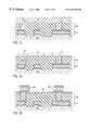
- Integrated circuit 100includes a substrate layer 102 , a first metal layer or stack 104 , and an interlayer dielectric 106 .
- Stack 104is 4400-13,000 ⁇ thick and comprised of layers similar to layer 72 , 74 , and 76 (FIG. 4 ).
- Interlayer dielectric 106is comprised of a first fluorinated silicon dioxide layer 108 and a second fluorinated silicon dioxide layer 109 .
- Fluorinated silicon dioxide layers 108 and 109have a dielectric constant between 3.5 and 3.7.
- the combination of layers 108 and 109have a thickness of 2.4 times the thickness of metal stack 104 .
- layer 106can be made of a single layer 108 of fluorinated silicon dioxide.
- a gap-filled fluorinated silicon dioxide depositionis utilized.
- a high etch/depth (HDP) ratio with high bias poweris utilized to form vias, as described below.
- the thickness of layer 108is 1.2 times the thickness of stack 104 .
- layer 106is subject to a chemical mechanical polish (CMP) and a cleaning treatment.
- CMPchemical mechanical polish
- an ammonia surface treatmentis performed to remove fluorine from a top surface 112 of region 106 .
- surface 112is depleted in a similar manner as surface 84 , discussed with reference to FIG. 6 .
- surface 112is subjected to an ammonia (NH 3 ) plasma.
- NH 3ammonia
- surface 112is subject to a passivation step similar to surface 64 , discussed with reference to FIG. 4, by utilizing a nitrite (NO 2 ⁇ ) plasma.
- layer 106is masked and etched to form holes for vias or contacts.
- surfaces 114are subject to depletion and passivation steps similar to the treatments, described with reference to FIG. 9 .
- Surfaces 114are similar to surface 96 , discussed with reference to FIG. 6 .
- apertures 116are filled with a metal, such as, a conformal layer 122 of tungsten.
- Conformal layer 122is subject to a CMP.
- the CMPcan effect the treatment on surface 112 .
- surface 112is again subjected to the depletion and passivation treatment, discussed with reference to FIG. 8, to remove the effects of the CMP treatment.
- a second metal layer 126is deposited over surface 112 .
- the second metal layer 126can be masked and etched.
Landscapes
- Engineering & Computer Science (AREA)
- Physics & Mathematics (AREA)
- Condensed Matter Physics & Semiconductors (AREA)
- General Physics & Mathematics (AREA)
- Computer Hardware Design (AREA)
- Microelectronics & Electronic Packaging (AREA)
- Power Engineering (AREA)
- Manufacturing & Machinery (AREA)
- Plasma & Fusion (AREA)
- Chemical & Material Sciences (AREA)
- Chemical Kinetics & Catalysis (AREA)
- Internal Circuitry In Semiconductor Integrated Circuit Devices (AREA)
Abstract
Description
Claims (20)
Priority Applications (1)
| Application Number | Priority Date | Filing Date | Title |
|---|---|---|---|
| US09/373,483US6444593B1 (en) | 1998-12-02 | 1999-08-12 | Surface treatment of low-K SiOF to prevent metal interaction |
Applications Claiming Priority (2)
| Application Number | Priority Date | Filing Date | Title |
|---|---|---|---|
| US09/203,572US6252303B1 (en) | 1998-12-02 | 1998-12-02 | Intergration of low-K SiOF as inter-layer dielectric |
| US09/373,483US6444593B1 (en) | 1998-12-02 | 1999-08-12 | Surface treatment of low-K SiOF to prevent metal interaction |
Related Parent Applications (1)
| Application Number | Title | Priority Date | Filing Date |
|---|---|---|---|
| US09/203,572Continuation-In-PartUS6252303B1 (en) | 1998-12-02 | 1998-12-02 | Intergration of low-K SiOF as inter-layer dielectric |
Publications (1)
| Publication Number | Publication Date |
|---|---|
| US6444593B1true US6444593B1 (en) | 2002-09-03 |
Family
ID=46276456
Family Applications (1)
| Application Number | Title | Priority Date | Filing Date |
|---|---|---|---|
| US09/373,483Expired - LifetimeUS6444593B1 (en) | 1998-12-02 | 1999-08-12 | Surface treatment of low-K SiOF to prevent metal interaction |
Country Status (1)
| Country | Link |
|---|---|
| US (1) | US6444593B1 (en) |
Cited By (10)
| Publication number | Priority date | Publication date | Assignee | Title |
|---|---|---|---|---|
| US20010033997A1 (en)* | 1998-02-25 | 2001-10-25 | Richard Holscher | Semiconductor processing methods |
| US20020020919A1 (en)* | 1998-12-23 | 2002-02-21 | Weimin Li | Semiconductor devices, and semiconductor processing methods |
| US20020146910A1 (en)* | 2000-01-18 | 2002-10-10 | Deboer Scott Jeffrey | Semiconductor processing methods of transferring patterns from patterned photoresists to materials, and structures comprising silicon nitride |
| US20030168745A1 (en)* | 2002-03-05 | 2003-09-11 | Yu-Sik Kim | Multi-layer structure for reducing capacitance and manufacturing method thereof |
| US6727173B2 (en) | 1998-09-03 | 2004-04-27 | Micron Technology, Inc. | Semiconductor processing methods of forming an utilizing antireflective material layers, and methods of forming transistor gate stacks |
| US7067414B1 (en)* | 1999-09-01 | 2006-06-27 | Micron Technology, Inc. | Low k interlevel dielectric layer fabrication methods |
| US20080176400A1 (en)* | 2007-01-23 | 2008-07-24 | Sumitomo Electric Industries, Ltd. | III-V Compound Semiconductor Substrate Manufacturing Method |
| US7576400B1 (en) | 1998-09-03 | 2009-08-18 | Micron Technology, Inc. | Circuitry and gate stacks |
| US7804115B2 (en) | 1998-02-25 | 2010-09-28 | Micron Technology, Inc. | Semiconductor constructions having antireflective portions |
| US20150123250A1 (en)* | 2013-11-04 | 2015-05-07 | Globalfoundries Inc. | Methods of fabricating defect-free semiconductor structures |
Citations (13)
| Publication number | Priority date | Publication date | Assignee | Title |
|---|---|---|---|---|
| US5703404A (en) | 1995-10-23 | 1997-12-30 | Mitsubishi Denki Kabushiki Kaisha | Semiconductor device comprising an SiOF insulative film |
| US5753975A (en) | 1994-09-01 | 1998-05-19 | Kabushiki Kaisha Toshiba | Semiconductor device with improved adhesion between titanium-based metal wiring layer and insulation film |
| US5789315A (en) | 1996-07-17 | 1998-08-04 | Advanced Micro Devices, Inc. | Eliminating metal extrusions by controlling the liner deposition temperature |
| US5807785A (en) | 1996-08-02 | 1998-09-15 | Applied Materials, Inc. | Low dielectric constant silicon dioxide sandwich layer |
| US5869149A (en)* | 1997-06-30 | 1999-02-09 | Lam Research Corporation | Method for preparing nitrogen surface treated fluorine doped silicon dioxide films |
| US5896149A (en) | 1995-06-12 | 1999-04-20 | Seiko Epson Corporation | Ink jet type recording head having a flow passage substrate with a stepped configuration and recesses formed in a surface thereof |
| US5994778A (en) | 1998-09-18 | 1999-11-30 | Advanced Micro Devices, Inc. | Surface treatment of low-k SiOF to prevent metal interaction |
| US6008120A (en) | 1998-07-22 | 1999-12-28 | Siemens Aktiengesellschaft | Silicon oxynitride cap for fluorinated silicate glass film in intermetal dielectric semiconductor fabrication |
| US6051321A (en) | 1997-10-24 | 2000-04-18 | Quester Technology, Inc. | Low dielectric constant materials and method |
| US6070550A (en) | 1996-09-12 | 2000-06-06 | Applied Materials, Inc. | Apparatus for the stabilization of halogen-doped films through the use of multiple sealing layers |
| US6103601A (en)* | 1995-10-26 | 2000-08-15 | Applied Materials, Inc. | Method and apparatus for improving film stability of halogen-doped silicon oxide films |
| US6136685A (en)* | 1997-06-03 | 2000-10-24 | Applied Materials, Inc. | High deposition rate recipe for low dielectric constant films |
| US6252303B1 (en) | 1998-12-02 | 2001-06-26 | Advanced Micro Devices, Inc. | Intergration of low-K SiOF as inter-layer dielectric |
- 1999
- 1999-08-12USUS09/373,483patent/US6444593B1/ennot_activeExpired - Lifetime
Patent Citations (13)
| Publication number | Priority date | Publication date | Assignee | Title |
|---|---|---|---|---|
| US5753975A (en) | 1994-09-01 | 1998-05-19 | Kabushiki Kaisha Toshiba | Semiconductor device with improved adhesion between titanium-based metal wiring layer and insulation film |
| US5896149A (en) | 1995-06-12 | 1999-04-20 | Seiko Epson Corporation | Ink jet type recording head having a flow passage substrate with a stepped configuration and recesses formed in a surface thereof |
| US5703404A (en) | 1995-10-23 | 1997-12-30 | Mitsubishi Denki Kabushiki Kaisha | Semiconductor device comprising an SiOF insulative film |
| US6103601A (en)* | 1995-10-26 | 2000-08-15 | Applied Materials, Inc. | Method and apparatus for improving film stability of halogen-doped silicon oxide films |
| US5789315A (en) | 1996-07-17 | 1998-08-04 | Advanced Micro Devices, Inc. | Eliminating metal extrusions by controlling the liner deposition temperature |
| US5807785A (en) | 1996-08-02 | 1998-09-15 | Applied Materials, Inc. | Low dielectric constant silicon dioxide sandwich layer |
| US6070550A (en) | 1996-09-12 | 2000-06-06 | Applied Materials, Inc. | Apparatus for the stabilization of halogen-doped films through the use of multiple sealing layers |
| US6136685A (en)* | 1997-06-03 | 2000-10-24 | Applied Materials, Inc. | High deposition rate recipe for low dielectric constant films |
| US5869149A (en)* | 1997-06-30 | 1999-02-09 | Lam Research Corporation | Method for preparing nitrogen surface treated fluorine doped silicon dioxide films |
| US6051321A (en) | 1997-10-24 | 2000-04-18 | Quester Technology, Inc. | Low dielectric constant materials and method |
| US6008120A (en) | 1998-07-22 | 1999-12-28 | Siemens Aktiengesellschaft | Silicon oxynitride cap for fluorinated silicate glass film in intermetal dielectric semiconductor fabrication |
| US5994778A (en) | 1998-09-18 | 1999-11-30 | Advanced Micro Devices, Inc. | Surface treatment of low-k SiOF to prevent metal interaction |
| US6252303B1 (en) | 1998-12-02 | 2001-06-26 | Advanced Micro Devices, Inc. | Intergration of low-K SiOF as inter-layer dielectric |
Non-Patent Citations (1)
| Title |
|---|
| Takeishi et al. ("Stabilizing dielectric constants of fluorine-doped SiO2 films by N20-plasma annealing", Journal of the Electrochemical Society, Jan. 1996, vol. 143, pp. 381-5).* |
Cited By (28)
| Publication number | Priority date | Publication date | Assignee | Title |
|---|---|---|---|---|
| US20010033997A1 (en)* | 1998-02-25 | 2001-10-25 | Richard Holscher | Semiconductor processing methods |
| US7825443B2 (en) | 1998-02-25 | 2010-11-02 | Micron Technology, Inc. | Semiconductor constructions |
| US7804115B2 (en) | 1998-02-25 | 2010-09-28 | Micron Technology, Inc. | Semiconductor constructions having antireflective portions |
| US7626238B2 (en) | 1998-02-25 | 2009-12-01 | Micron Technology, Inc. | Semiconductor devices having antireflective material |
| US6878507B2 (en) | 1998-02-25 | 2005-04-12 | Micron Technology, Inc. | Semiconductor processing methods |
| US20040180537A1 (en)* | 1998-09-03 | 2004-09-16 | Micron Technology, Inc. | Semiconductor processing methods of forming and utilizing antireflective material layers, and methods of forming transistor gate stacks |
| US7151054B2 (en) | 1998-09-03 | 2006-12-19 | Micron Technology, Inc. | Semiconductor processing methods of forming and utilizing antireflective material layers, and methods of forming transistor gate stacks |
| US6727173B2 (en) | 1998-09-03 | 2004-04-27 | Micron Technology, Inc. | Semiconductor processing methods of forming an utilizing antireflective material layers, and methods of forming transistor gate stacks |
| US7576400B1 (en) | 1998-09-03 | 2009-08-18 | Micron Technology, Inc. | Circuitry and gate stacks |
| US20020020919A1 (en)* | 1998-12-23 | 2002-02-21 | Weimin Li | Semiconductor devices, and semiconductor processing methods |
| US7279118B2 (en) | 1998-12-23 | 2007-10-09 | Micron Technology, Inc. | Compositions of matter and barrier layer compositions |
| US7067414B1 (en)* | 1999-09-01 | 2006-06-27 | Micron Technology, Inc. | Low k interlevel dielectric layer fabrication methods |
| US7521354B2 (en) | 1999-09-01 | 2009-04-21 | Micron Technology, Inc. | Low k interlevel dielectric layer fabrication methods |
| US7078356B2 (en) | 1999-09-01 | 2006-07-18 | Micron Technology, Inc. | Low K interlevel dielectric layer fabrication methods |
| US6858523B2 (en) | 2000-01-18 | 2005-02-22 | Micron Technology, Inc. | Semiconductor processing methods of transferring patterns from patterned photoresists to materials, and structures comprising silicon nitride |
| US20020151160A1 (en)* | 2000-01-18 | 2002-10-17 | Deboer Scott Jeffrey | Semiconductor processing methods of transferring patterns from patterned photoresists to materials, and structures comprising silicon nitride |
| US7045277B2 (en) | 2000-01-18 | 2006-05-16 | Micron Technology, Inc. | Semiconductor processing methods of transferring patterns from patterned photoresists to materials, and structures comprising silicon nitride |
| US7078328B2 (en) | 2000-01-18 | 2006-07-18 | Micron Technology, Inc. | Semiconductor processing methods of transferring patterns from patterned photoresists to materials, and structures comprising silicon nitride |
| US7435688B2 (en) | 2000-01-18 | 2008-10-14 | Micron Technology, Inc. | Semiconductor processing methods of transferring patterns from patterned photoresists to materials, and structures comprising silicon nitride |
| US20020146910A1 (en)* | 2000-01-18 | 2002-10-10 | Deboer Scott Jeffrey | Semiconductor processing methods of transferring patterns from patterned photoresists to materials, and structures comprising silicon nitride |
| US7638436B2 (en) | 2000-01-18 | 2009-12-29 | Micron Technology, Inc. | Semiconductor processing methods of transferring patterns from patterned photoresists to materials |
| US7208805B2 (en) | 2000-01-18 | 2007-04-24 | Micron Technology, Inc. | Structures comprising a layer free of nitrogen between silicon nitride and photoresist |
| US20030168745A1 (en)* | 2002-03-05 | 2003-09-11 | Yu-Sik Kim | Multi-layer structure for reducing capacitance and manufacturing method thereof |
| US6747292B2 (en)* | 2002-03-05 | 2004-06-08 | Samsung Electronics Co., Ltd. | Multi-layer structure for reducing capacitance and manufacturing method thereof |
| US20080176400A1 (en)* | 2007-01-23 | 2008-07-24 | Sumitomo Electric Industries, Ltd. | III-V Compound Semiconductor Substrate Manufacturing Method |
| US7960284B2 (en)* | 2007-01-23 | 2011-06-14 | Sumitomo Electric Industries, Ltd. | III-V compound semiconductor substrate manufacturing method |
| US20150123250A1 (en)* | 2013-11-04 | 2015-05-07 | Globalfoundries Inc. | Methods of fabricating defect-free semiconductor structures |
| US9142422B2 (en)* | 2013-11-04 | 2015-09-22 | Globalfoundries Inc | Methods of fabricating defect-free semiconductor structures |
Similar Documents
| Publication | Publication Date | Title |
|---|---|---|
| US7799693B2 (en) | Method for manufacturing a semiconductor device | |
| US7888261B2 (en) | Barrier-metal-free copper damascene technology using atomic hydrogen enhanced reflow | |
| US6400023B2 (en) | Integration of low-k SiOF for damascene structure | |
| US6136680A (en) | Methods to improve copper-fluorinated silica glass interconnects | |
| US6479380B2 (en) | Semiconductor device and manufacturing method thereof | |
| US6177364B1 (en) | Integration of low-K SiOF for damascene structure | |
| US6335273B2 (en) | Surface treatment of low-K SiOF to prevent metal interaction | |
| US20070197023A1 (en) | Entire encapsulation of Cu interconnects using self-aligned CuSiN film | |
| US20040084680A1 (en) | Barrier layer for a copper metallization layer including a low k dielectric | |
| US20020173142A1 (en) | Method of fabricating a semiconductor device | |
| JPH10189733A (en) | Metal coating method for porous dielectric | |
| US20100301486A1 (en) | High-aspect ratio contact element with superior shape in a semiconductor device for improving liner deposition | |
| US6146996A (en) | Semiconductor device with conductive via and method of making same | |
| US6444593B1 (en) | Surface treatment of low-K SiOF to prevent metal interaction | |
| JP2000091422A (en) | Method for manufacturing multilayer wiring structure | |
| US20050242430A1 (en) | Multi-level semiconductor device with capping layer with improved adhesion | |
| US6281584B1 (en) | Integrated circuit with improved adhesion between interfaces of conductive and dielectric surfaces | |
| US20030209805A1 (en) | Flourine doped SiO2 film and method of fabrication | |
| US6599838B1 (en) | Method for forming metal filled semiconductor features to improve a subsequent metal CMP process | |
| US7381660B2 (en) | Dielectric barrier layer for a copper metallization layer having a varying silicon concentration along its thickness | |
| JP5217272B2 (en) | Wiring forming method and semiconductor device manufacturing method | |
| US20070037378A1 (en) | Method for forming metal pad in semiconductor device | |
| JP2000323569A (en) | Semiconductor integrated circuit device and method of manufacturing the same | |
| KR100738578B1 (en) | Metal wiring formation method of semiconductor device | |
| JP2000277611A (en) | Manufacture of semiconductor device |
Legal Events
| Date | Code | Title | Description |
|---|---|---|---|
| AS | Assignment | Owner name:ADVANCED MICRO DEVICES, INC., CALIFORNIA Free format text:ASSIGNMENT OF ASSIGNORS INTEREST;ASSIGNORS:NGO, MINH VAN;HUANG, RICHARD J.;MORALES, GUARIONEX;REEL/FRAME:010174/0288;SIGNING DATES FROM 19990719 TO 19990729 | |
| STCF | Information on status: patent grant | Free format text:PATENTED CASE | |
| FEPP | Fee payment procedure | Free format text:PAYOR NUMBER ASSIGNED (ORIGINAL EVENT CODE: ASPN); ENTITY STATUS OF PATENT OWNER: LARGE ENTITY | |
| FPAY | Fee payment | Year of fee payment:4 | |
| AS | Assignment | Owner name:GLOBALFOUNDRIES INC., CAYMAN ISLANDS Free format text:AFFIRMATION OF PATENT ASSIGNMENT;ASSIGNOR:ADVANCED MICRO DEVICES, INC.;REEL/FRAME:023119/0083 Effective date:20090630 | |
| FPAY | Fee payment | Year of fee payment:8 | |
| FPAY | Fee payment | Year of fee payment:12 | |
| AS | Assignment | Owner name:WILMINGTON TRUST, NATIONAL ASSOCIATION, DELAWARE Free format text:SECURITY AGREEMENT;ASSIGNOR:GLOBALFOUNDRIES INC.;REEL/FRAME:049490/0001 Effective date:20181127 | |
| AS | Assignment | Owner name:GLOBALFOUNDRIES INC., CAYMAN ISLANDS Free format text:RELEASE BY SECURED PARTY;ASSIGNOR:WILMINGTON TRUST, NATIONAL ASSOCIATION;REEL/FRAME:054636/0001 Effective date:20201117 | |
| AS | Assignment | Owner name:GLOBALFOUNDRIES U.S. INC., NEW YORK Free format text:RELEASE BY SECURED PARTY;ASSIGNOR:WILMINGTON TRUST, NATIONAL ASSOCIATION;REEL/FRAME:056987/0001 Effective date:20201117 |