US6444586B2 - Method of etching doped silicon dioxide with selectivity to undoped silicon dioxide with a high density plasma etcher - Google Patents
Method of etching doped silicon dioxide with selectivity to undoped silicon dioxide with a high density plasma etcherDownload PDFInfo
- Publication number
- US6444586B2 US6444586B2US09/932,601US93260101AUS6444586B2US 6444586 B2US6444586 B2US 6444586B2US 93260101 AUS93260101 AUS 93260101AUS 6444586 B2US6444586 B2US 6444586B2
- Authority
- US
- United States
- Prior art keywords
- layer
- silicon dioxide
- high density
- doped silicon
- density plasma
- Prior art date
- Legal status (The legal status is an assumption and is not a legal conclusion. Google has not performed a legal analysis and makes no representation as to the accuracy of the status listed.)
- Expired - Lifetime
Links
Images


Classifications
- H—ELECTRICITY
- H01—ELECTRIC ELEMENTS
- H01L—SEMICONDUCTOR DEVICES NOT COVERED BY CLASS H10
- H01L21/00—Processes or apparatus adapted for the manufacture or treatment of semiconductor or solid state devices or of parts thereof
- H01L21/70—Manufacture or treatment of devices consisting of a plurality of solid state components formed in or on a common substrate or of parts thereof; Manufacture of integrated circuit devices or of parts thereof
- H01L21/71—Manufacture of specific parts of devices defined in group H01L21/70
- H01L21/768—Applying interconnections to be used for carrying current between separate components within a device comprising conductors and dielectrics
- H01L21/76801—Applying interconnections to be used for carrying current between separate components within a device comprising conductors and dielectrics characterised by the formation and the after-treatment of the dielectrics, e.g. smoothing
- H01L21/76802—Applying interconnections to be used for carrying current between separate components within a device comprising conductors and dielectrics characterised by the formation and the after-treatment of the dielectrics, e.g. smoothing by forming openings in dielectrics
- H01L21/76807—Applying interconnections to be used for carrying current between separate components within a device comprising conductors and dielectrics characterised by the formation and the after-treatment of the dielectrics, e.g. smoothing by forming openings in dielectrics for dual damascene structures
- H01L21/76808—Applying interconnections to be used for carrying current between separate components within a device comprising conductors and dielectrics characterised by the formation and the after-treatment of the dielectrics, e.g. smoothing by forming openings in dielectrics for dual damascene structures involving intermediate temporary filling with material
- H—ELECTRICITY
- H01—ELECTRIC ELEMENTS
- H01L—SEMICONDUCTOR DEVICES NOT COVERED BY CLASS H10
- H01L21/00—Processes or apparatus adapted for the manufacture or treatment of semiconductor or solid state devices or of parts thereof
- H01L21/02—Manufacture or treatment of semiconductor devices or of parts thereof
- H01L21/04—Manufacture or treatment of semiconductor devices or of parts thereof the devices having potential barriers, e.g. a PN junction, depletion layer or carrier concentration layer
- H01L21/18—Manufacture or treatment of semiconductor devices or of parts thereof the devices having potential barriers, e.g. a PN junction, depletion layer or carrier concentration layer the devices having semiconductor bodies comprising elements of Group IV of the Periodic Table or AIIIBV compounds with or without impurities, e.g. doping materials
- H01L21/30—Treatment of semiconductor bodies using processes or apparatus not provided for in groups H01L21/20 - H01L21/26
- H01L21/31—Treatment of semiconductor bodies using processes or apparatus not provided for in groups H01L21/20 - H01L21/26 to form insulating layers thereon, e.g. for masking or by using photolithographic techniques; After treatment of these layers; Selection of materials for these layers
- H01L21/3105—After-treatment
- H01L21/311—Etching the insulating layers by chemical or physical means
- H01L21/31105—Etching inorganic layers
- H01L21/31111—Etching inorganic layers by chemical means
- H01L21/31116—Etching inorganic layers by chemical means by dry-etching
- H—ELECTRICITY
- H01—ELECTRIC ELEMENTS
- H01L—SEMICONDUCTOR DEVICES NOT COVERED BY CLASS H10
- H01L21/00—Processes or apparatus adapted for the manufacture or treatment of semiconductor or solid state devices or of parts thereof
- H01L21/70—Manufacture or treatment of devices consisting of a plurality of solid state components formed in or on a common substrate or of parts thereof; Manufacture of integrated circuit devices or of parts thereof
- H01L21/71—Manufacture of specific parts of devices defined in group H01L21/70
- H01L21/768—Applying interconnections to be used for carrying current between separate components within a device comprising conductors and dielectrics
- H01L21/76801—Applying interconnections to be used for carrying current between separate components within a device comprising conductors and dielectrics characterised by the formation and the after-treatment of the dielectrics, e.g. smoothing
- H01L21/76802—Applying interconnections to be used for carrying current between separate components within a device comprising conductors and dielectrics characterised by the formation and the after-treatment of the dielectrics, e.g. smoothing by forming openings in dielectrics
- H—ELECTRICITY
- H01—ELECTRIC ELEMENTS
- H01L—SEMICONDUCTOR DEVICES NOT COVERED BY CLASS H10
- H01L21/00—Processes or apparatus adapted for the manufacture or treatment of semiconductor or solid state devices or of parts thereof
- H01L21/70—Manufacture or treatment of devices consisting of a plurality of solid state components formed in or on a common substrate or of parts thereof; Manufacture of integrated circuit devices or of parts thereof
- H01L21/71—Manufacture of specific parts of devices defined in group H01L21/70
- H01L21/768—Applying interconnections to be used for carrying current between separate components within a device comprising conductors and dielectrics
- H01L21/76897—Formation of self-aligned vias or contact plugs, i.e. involving a lithographically uncritical step
- H—ELECTRICITY
- H01—ELECTRIC ELEMENTS
- H01L—SEMICONDUCTOR DEVICES NOT COVERED BY CLASS H10
- H01L2221/00—Processes or apparatus adapted for the manufacture or treatment of semiconductor or solid state devices or of parts thereof covered by H01L21/00
- H01L2221/10—Applying interconnections to be used for carrying current between separate components within a device
- H01L2221/1005—Formation and after-treatment of dielectrics
- H01L2221/101—Forming openings in dielectrics
- H01L2221/1015—Forming openings in dielectrics for dual damascene structures
- H01L2221/1031—Dual damascene by forming vias in the via-level dielectric prior to deposition of the trench-level dielectric
Definitions
- the present inventionrelates to removing doped silicon dioxide from a structure in a process that is selective to undoped silicon dioxide. More particularly, the present invention is directed to a method of using a high density plasma etcher such that doped silicon dioxide is removed from a structure at a material removal rate that is greater than that of undoped silicon dioxide.
- semiconductor substrateis defined to mean any construction comprising semiconductive material, including but not limited to bulk semiconductive material such as a semiconductive wafer, either alone or in assemblies comprising other materials thereon, and semiconductive material layers, either alone or in assemblies comprising other materials.
- substraterefers to any supporting structure including but not limited to the semiconductive substrates described above.
- doped silicon dioxiderefers to silicon dioxide having a dopant concentration greater than or equal to about 3% by weight.
- the term “undoped silicon dioxide”is defined as silicon dioxide having a dopant concentration less than about 3% by weight.
- semiconductor industryis attempting to increase the speed at which integrated circuits operate, to increase the density of devices on integrated circuits, and to reduce the price of integrated circuits.
- semiconductor devicesincluding capacitors, resistors, transistors, diodes, and the like, are continually being increased in number and decreased in dimension in a process known as miniaturization.
- miniaturizationIn advanced manufacturing of integrated circuits, hundreds of thousands of these semiconductor devices are formed on a single semiconductor substrate. Efficient packing of these devices requires multilayer topographical design.
- One common process for forming a topographical design on a semiconductor substrateinvolves etching of semiconductor material.
- the dimensional extent of material removal during an etch processis typically controlled by providing etch-resistant materials in predetermined regions of a semiconductor substrate.
- An etch-resistant structure that shields underlying material from an etchis known as an etch mask, while etch-resistant material positioned beneath material to be removed is an etch stop.
- the etch processis substantially selective to the etch stop or etch mask, while being not selective to the material to be removed.
- an etch-resistant masking layeris deposited and patterned over the semiconductor material to be etched.
- the pattern formed on the layer of masking materialdefines a series of openings in the masking material and corresponds to the topographical design to be formed during the etching process.
- an etchantis applied to the semiconductor material through the pattern openings.
- a material, which may be doped silicon dioxide,is removed through the pattern openings, while the etch mask protects material positioned directly therebelow.
- photoresist materialis commonly used as an etch mask.
- photoresist material in an etch processinvolves forming, developing, and patterning the photoresist material, applying an etchant to etch the silicon dioxide, and then removing the photoresist material.
- the multiple steps involved in using photoresist materialrequire time and resources that can increase the cost of producing integrated circuits.
- an etch-resistant materialsuch as silicon nitride is commonly used as an etch stop or etch mask material, particularly in connection with etch processes of silicon dioxide with a fluorinated etch chemistry.
- silicon nitrideis usually used on top of a gate stack as an etch stop. The silicon nitride cap prevents overetching and ensures that the resulting contact hole is aligned directly atop the active region.
- silicon nitride capis the simultaneous formation of a silicon nitride layer on the back side of a semiconductor wafer.
- the particular problemsdepend on the process flow. For instance, where a low pressure chemical vapor deposition is used to deposit silicon nitride, both sides of the semiconductor wafer would receive deposits of silicon nitride.
- the presence of silicon nitride on the back side of the semiconductor wafercauses stress which deforms the shape of the semiconductor wafer, and can also potentially cause deformation of the crystal structure as well as cause defects in the circuit.
- silicon nitride depositionis inherently a dirty operation having particulate matter in abundance which tends to reduce yield. When a low pressure chemical vapor deposition process is utilized, the silicon nitride layering on the back side of the semiconductor wafer must be removed later in the process flow.
- the present inventionrelates to etching doped silicon dioxide from a structure in a process that is selective to undoped silicon dioxide.
- a structureis provided having a first region substantially composed of doped silicon dioxide and a second region substantially composed of undoped silicon dioxide. The first and second regions are configured to define a topographical structure to be formed by the selective etch process.
- a high density plasma systemis used to remove doped silicon dioxide from the topographical structure.
- a high density plasma systemhas two electrodes.
- the two electrodesare the upper electrode and lower electrode. There is a space or gap between the two electrodes.
- the upper electrodeis sometimes referred to as the upper window.
- An inductively coupled plasmais usually applied to the upper electrode (or upper window).
- the power that is applied to the upper electrodecan be divided into two parts, such as an outer coil and an inner coil.
- the power that is applied to the upper electrodeis usually referred to, and is referred to herein, as the source power.
- a semiconductor substrate of a wafer being etchedis situated on the lower electrode where an optional RF power is usually applied thereto. This power is usually referred as to the bias power.
- the etch under these conditionhas a plasma density not less than about 10 9 cm ⁇ 3 , and the operating pressure is usually at 10 Millitorr (mT) or below.
- a high density plasma source with a fluorinated etch chemistryis applied to the structure such that an inductively-coupled power is delivered to the upper electrode in an amount less than about 1000 Watts (W) per 200 mm-diameter wafer surface. Stated otherwise, the source power density can be expressed as an amount less than about 0.032 W/mm 2 or 19.89 W/in 2 . Accordingly, doped silicon dioxide is removed from the structure at a material removal rate that is greater than the rate of removal of undoped silicon dioxide.
- the bottom electrodeIn a reactive ion etcher (RIE), only the bottom electrode where the wafer is situated is powered. Thus, the bottom electrode is preferably the same size as the wafer.
- the power densityis defined as the ratio between the power and the wafer surface area.
- the source power which generates a plasma in the etcheris applied to the upper electrode or upper window.
- a coilis situated on the upper window. There is generally no definite shape or size of the coil that sits on the upper window and the size or volume of the plasma zone is not necessarily the same as the size of the coil.
- the power densityis defined as the source power applied to the upper window over the surface area of the wafer situated upon the bottom electrode.
- the method of the inventionextends to any structure from which doped silicon dioxide may be removed selectively to undoped silicon dioxide.
- the inventionhas been found particularly advantageous for use in semiconductor structure fabrication.
- a doped silicon dioxide layeris formed over a semiconductor substrate.
- An undoped silicon dioxide layeris then formed over the doped silicon dioxide and patterned to provide one or more openings therein extending to the doped silicon dioxide layer.
- the high density plasma etch process described aboveis conducted, thereby selectively removing doped silicon dioxide through the openings in the pattern and forming a predetermined topographical structure.
- the undoped silicon dioxide layeracts as an etch mask during the etching process. Under this embodiment, the undoped silicon dioxide etch mask does not need to be removed after the etching process is completed.
- the positions of the doped and the undoped silicon dioxide layers within the structureare reversed.
- the undoped silicon dioxide layeris formed over the semiconductor substrate, with the doped silicon dioxide layer formed thereupon.
- Photoresistis deposited and patterned on doped silicon dioxide to provide openings.
- the high density plasma etchis directed onto the structure, thereby removing doped silicon dioxide to form an opening that terminates at the undoped silicon dioxide layer.
- the inventionis useful with a variety of applications wherein doped silicon dioxide is etched from a semiconductor structure.
- undoped silicon dioxide layersmay be positioned both over and under a doped silicon dioxide layer.
- the inventionmay be used for forming a self-aligned contact hole to a contact surface on a semiconductor substrate.
- the self-aligned contact holeis formed by first providing a multilayer structure over the semiconductor substrate that comprises a thin silicon dioxide layer, a layer of conductor material, and a refractory metal silicide layer.
- the multilayer structuremay include a gate oxide layer, a polysilicon layer, and a refractory metal silicide layer successively formed over a semiconductor substrate.
- An undoped silicon dioxide layeris then formed over the multilayer structure.
- the multilayer structureis patterned to form the designated topography, with openings extending to the semiconductor substrate.
- Doped silicon dioxideis next formed over the semiconductor substrate.
- a patterned etch mask layeris utilized to expose selected portions of the doped silicon dioxide layer that are intended to be etched.
- One example of a topographical structure created utilizing this processare gate stacks.
- a high density plasma etch as described aboveis conducted to selectively and anisotropically remove doped silicon dioxide such that a self-aligned contact opening extends to a contact surface on the semiconductor substrate between the gate stacks.
- the present inventionprovides undoped silicon dioxide as an alternative to silicon nitride that has previously been used in many selective etch processes.
- the use of photoresist material that must be removed after etchingis reduced or eliminated under the invention.
- the etching process of the inventionmay be conducted with high density plasma etchers.
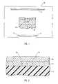
- FIG. 1is a partial cross-sectional elevation view of a multilayer structure in a high density plasma etcher that is etched according to one embodiment of the invention.
- An undoped silicon dioxide layeris formed over a doped silicon dioxide layer and patterned.
- a high density plasma etchis conducted to selectively remove doped silicon dioxide.
- FIG. 2is a partial cross-sectional elevation view of a preliminary step according to another embodiment of the invention, wherein an opening is formed in an undoped silicon dioxide layer.
- FIG. 3is a partial cross-sectional elevation view of the structure of FIG. 2.
- a doped silicon dioxide layeris formed and selectively removed with a high density plasma etch such that the underlying undoped silicon dioxide layer acts as an etch stop.
- FIG. 4is a partial cross-sectional elevation view of a structure from which gate stacks are to be formed according to the invention.
- FIG. 5is a partial cross-sectional elevation view of formation of a contact opening between a pair of gate stacks.
- the gate stackshave an upper undoped silicon dioxide layer and undoped silicon dioxide spacers to which a high density plasma etch is selective.
- FIG. 6is a partial cross-sectional elevation view of another embodiment of the invention in which two contact openings are successively formed.
- Undoped silicon dioxideis used as both an etch stop and an etch mask during the formation of contact openings between pairs of gate stacks.
- a photoresist layeris used to substantially fill a second opening during etching through a first opening in an intermediate step of the process.
- FIG. 7is a partial cross-sectional elevation view of a variation of the embodiment of FIG. 5 .
- An upper pair of gate stackseach of which has an undoped silicon dioxide upper layer and an undoped silicon dioxide spacer, is positioned to be an etch mask for the high density plasma etch.
- a lower pair of gate stacksare positioned to be an etch stop and to form a self-aligned contact opening.
- the present inventionrelates to etching doped silicon dioxide from a structure in a process that is selective to undoped silicon dioxide.
- a structureis provided having a first region substantially composed of doped silicon dioxide and a second region substantially composed of undoped silicon dioxide.
- the first and second regionsare configured to define a topographical structure to be formed by the selective etch process. Often, the first and second regions will be in physical contact one with another.
- a high density plasma etch with a fluorinated etch chemistryis applied to the structure such that a power density is delivered to both of the first and second regions in an amount less than about 1000 W per 200-mm diameter wafer. Accordingly, doped silicon dioxide is removed from the structure at a material removal rate that is greater than the rate of removal of undoped silicon dioxide.
- high density plasma etchis any plasma etch conducted in a high density plasma etcher in which there is an ion density higher than about 10 9 ions/cm 3 .
- RIEreactive ion etching
- MIEmagnetically enhanced reactive ion etching
- High density plasma etchersare notable for the high material removal rates which they produce. Typical high density plasma etch rates of silicon dioxide are in a range from about 5,000 ⁇ /min to about 10,000 ⁇ /min. RIE processes ordinarily do not exceed about 5,000 ⁇ /min.
- material removal rateis expressed as a unit length per unit time.
- a material removal rate as expressed hereinis measured only over the amount of time during which a surface of the material is actually exposed to an etch chemistry. For example, if a certain embodiment includes a second layer exposed by etching an opening through a first layer, the material removal rate of the first layer is calculated only during the time in which the opening is being formed therein, while the material removal rate of the second layer is measured only during the time after which a surface thereof is exposed to an etch chemistry through the opening. This method of measuring material removal rates allows objective and consistent comparison between surfaces that may be exposed during different lengths of time.
- High density etchersmay be used in a range of operating parameters, including those of power density, which is defined as the energy rate delivered to a surface of a structure to be etched per unit area.
- power densitywhich is defined as the energy rate delivered to a surface of a structure to be etched per unit area.
- high density plasma etchershave been used at or near their maximum power density, in a range of about 1000 W per 200-mm diameter wafer or higher. This range of power density is referred to herein as “high power density.”
- High density plasma etchersare also capable of delivering less energy, including “medium power density” which is herein defined as a range from less than about 1000 W per 200-mm diameter wafer and “low power density” which is herein defined as a range less than about 300 W per 200-mm diameter wafer.
- medium power densitywhich is herein defined as a range from less than about 1000 W per 200-mm diameter wafer
- low power densitywhich is herein defined as a range less than about 300 W per 200-mm diameter wa
- doped silicon dioxidemay be removed according to the invention at rates 10 times or more greater than the material removal rate of undoped silicon dioxide removal. While not fully understood, it is believed that deposition of polymers on exposed undoped silicon dioxide during the high density plasma etch plays some role in providing the selectivity to undoped silicon dioxide. Such polymers are generated during the chemical reactions between the etch chemistry and the material that is removed during the etch.
- the general etch process according to the preferred embodiments of the inventionis conducted by placing a wafer or other structure to be etched within a chamber of a high density plasma etcher.
- a typical waferis roughly circular and has a diameter of about 8 inches.
- Medium and low power densitiesare generated by controlling the power supply delivered to an upper electrode and a lower electrode within the chamber of the high density plasma etcher. Accordingly, for an 8 inch wafer, a source power is applied to the upper electrode in a range from about 500 Watts to about 1,000 Watts for medium power density or in a range less than about 500 Watts for low power density.
- a bias power, P Bis delivered to the lower electrode at an amount defined as P S ⁇ 200 ⁇ P B ⁇ P S +200, where P S is the source power as defined above.
- P Sis the source power as defined above.
- P S ⁇ 100 ⁇ P B ⁇ P S +100, and most preferably, the source power and the bias powerare about equal.
- the high density plasma etcherpreferably uses a fluorinated etch chemistry selected from the group of C 2 F 6 , CF 4 , C 3 F 8 , C 4 F 10 , CH 2 F 2 , CHF 3 , C 2 HF 5 , CH 3 F and combinations thereof.
- fluorinated etchantsin a substantially gas phase that can be employed during the etching of the structure.
- An inert gasis often used in combination with the fluorinated etchant.
- Argon, nitrogen, and heliumare examples of such an inert gas.
- the most preferred gassesare C 2 HF 5 , CH 2 F 2 , CHF 3 and Ar.
- CH 3 Fmay be used in place of CH 2 F 2 .
- preferred etchantsinclude a fluorine deficient gas, which is defined as a gas without enough fluorine atoms to saturate the bonding for the carbon atoms.
- temperature during a high density plasma etchis controlled by cooling the lower electrode with a fluid , such as water, having a temperature in a range from about 0° C. to about 30° C.
- a fluidsuch as water
- the upper limit of acceptable wafer temperaturesis defined by the softening temperature of photoresist material at about 130° C.
- the appropriate operating pressureis a function of the etch chemistry, among other factors, and will be understood by one skilled in the art. In most cases, however, the preferred pressure for a high density plasma etcher will be in a range from about 1 millitorr to about 10 millitorr.
- the high density plasma etch with the associated medium and low power densities as disclosed aboveare generally applicable to the various embodiments of the inventive methods as described herein.
- an 8 inch semiconductor waferwas placed within a high density plasma etcher.
- a source power of about 800 Wattswas delivered to the upper electrode, and a bias power of about 800 Watts was applied to the lower electrode.
- the etchwas conducted in a chemistry of C 2 HF 5 , CHF 3 and CH 2 F 2 , in a ratio of about 4:3:3, and at an operating pressure of about 3 millitorr.
- FIGS. 1-7illustrate methods of the invention as directed to several structures that may be formed by removal of doped silicon dioxide selective to undoped silicon dioxide.
- FIG. 1shows a high density plasma etcher 10 having an upper electrode 11 , a lower electrode 13 , and a stream of a cooling fluid 15 .
- a semiconductor substrate 12that preferably comprises silicon, and may be substantially composed of monocrystalline silicon, is also illustrated in FIG. 1 .
- Overlying semiconductor substrate 12is a first layer 14 substantially composed of doped silicon dioxide.
- first layer 14 and other doped silicon dioxide structures disclosed hereinare substantially composed of borophosphosilicate glass (BPSG), borosilicate glass (BSG), or phosphosilicate glass (PSG).
- BPSGborophosphosilicate glass
- BSGborosilicate glass
- PSGphosphosilicate glass
- first layer 14is substantially composed of silicon dioxide having a boron dopant concentration of about 3% or more by weight and a phosphorus dopant concentration of about 3% or more by weight.
- first layerrefers to a layer substantially composed of doped silicon dioxide.
- a second layer 16 substantially composed of undoped silicon dioxideis formed over first layer 14 .
- second layerrefers to a layer substantially composed of undoped silicon dioxide.
- the undoped silicon dioxide of second layer 16may be formed, for example, by a thermal process, by a plasma enhanced deposition process, by conventional TEOS precursor deposition that is preferably rich in carbon or hydrogen, or by a precursor of gaseous silane (SiH 4 ) with oxygen.
- Second layer 16is processed to form a first selected pattern 18 through which first layer 14 is exposed.
- the structure seen in FIG. 1is then etched according to the high density plasma etch described above.
- the preferred etchremoves doped silicon dioxide anisotropically from first layer 14 in a region aligned with first selected pattern 18 down to semiconductor substrate 12 .
- the high density plasma etchwill form an opening 20 (shown in phantom) having lateral dimensions substantially corresponding to those of first selected pattern 18 .
- opening 20will be defined by a contact surface 24 situated on semiconductor substrate 12 and a sidewall 22 that is substantially orthogonal to semiconductor substrate 12 .
- Second layer 16prevents the high density plasma etch from removing material from first layer 14 except as aligned with first selected pattern 18 .
- a contact plugsubstantially composed of a conductive material may be formed within opening 20 to provide electrical connection between contact surface 24 and overlying layers.
- a contact plugis defined by first selected pattern 18 and opening 20 and is illustrated by phantom lines in FIG. 1 .
- the contact plugis formed according to well-understood processes in the art.
- a structuresuch a contact plug may be formed in contact openings that extend to a contact surface on a semiconductor substrate.
- FIGS. 2 and 3depict another structure to which the etch process of the invention is applied wherein doped silicon dioxide is formed over undoped silicon dioxide.
- a second layer 16 substantially composed of undoped silicon dioxideis formed over a semiconductor substrate 12 .
- the undoped silicon dioxidemay be formed by any conventional process, including a thermal process, a plasma enhanced deposition process, a conventional TEOS precursor deposition that is preferably rich in carbon or hydrogen, or a precursor of gaseous silane (SiH 4 ) with oxygen.
- a photoresist layer 26is formed over second layer 16 and patterned to produce a first selected pattern 28 .
- Second layer 16is then anisotropically etched through first selected pattern 28 to selectively remove undoped silicon dioxide therefrom.
- the anisotropic etch of second layer 16may be any conventional etch process used in the art. Accordingly, opening 30 (shown in phantom) is formed through second layer 16 , thereby exposing semiconductor substrate 12 and forming undoped silicon dioxide caps 17 as seen in FIG. 3.
- a first layer 14 substantially composed of doped silicon dioxideis deposited over undoped silicon dioxide caps 17 and semiconductor substrate 12 as a passivation layer.
- An etch mask layer 32is formed over first layer 14 , and may be substantially composed of undoped silicon dioxide. Alternatively etch mask layer 32 may consist of a photoresist material or another suitable material that is resistant to a high density plasma etch. Etch mask layer 32 is patterned to form second selected pattern 34 substantially vertically aligned with opening 30 .
- the structure seen in FIG. 3is then etched according to the high density plasma etch of the invention as described above.
- the preferred etchremoves doped silicon dioxide anisotropically from first layer 14 in a region aligned with second selected pattern 34 down to semiconductor substrate 12 and second layer 16 .
- the high density plasma etchwill form contact opening 36 having lateral dimensions substantially corresponding to those of second selected pattern 34 and opening 30 .
- Undoped silicon dioxide caps 17prevent overetching of contact opening 36 , restricting the extent of exposure of semiconductor substrate 12 to contact surface 24 that is positioned between undoped silicon dioxide caps 17 .
- etch mask layer 32prevents the high density plasma etch from removing material from first layer 14 except as aligned with second selected pattern 34 . Accordingly, contact opening 36 is self-aligned with contact surface 24 .
- the high density plasma etch of the inventionthat is selective to undoped silicon dioxide avoids the need to use silicon nitride as an etch stop structure.
- a further embodiment of the method of the inventionis used to form one or more gate stacks as illustrated in FIGS. 4 and 5.
- a multilayer structure 50is formed over semiconductor substrate 12 .
- Multilayer structure 50comprises a gate oxide layer 38 that covers semiconductor substrate 12 .
- Gate oxide layer 38may be relatively thin in comparison with the other layers of multilayer structure 50 .
- a polysilicon layer 40is formed over gate oxide layer 38 .
- Overlying polysilicon layer 40is a refractory metal silicide layer 42 .
- a known benefit of refractory metal silicidesis their low resistivity.
- Refractory metal silicide layer 42for purposes of the invention described herein includes a silicide of at least one of titanium, chromium, tantalum, platinum, tungsten and zirconium, and also molybdenum.
- refractory metal silicide layer 42is substantially composed of tungsten silicide (WSi x ).
- refractory metal silicide layer 42Overlying refractory metal silicide layer 42 is a second layer 16 that is substantially composed of undoped silicon dioxide which can be formed by any known means including thermally, by plasma enhanced deposition, by a conventional TEOS precursor deposition that is preferably rich in carbon or hydrogen, or by a precursor of gaseous silane (SiH 4 ) with oxygen.
- a photoresist layer 26is provided and patterned over second layer 16 to form first selected pattern 28 .
- Multilayer structure 50is anisotropically etched through first selected pattern 28 to selectively remove material therefrom so as to form gate stacks 48 as illustrated in FIG. 5 .
- the etch of multilayer structure 50may be any conventional etch process used in the art.
- Each gate stack 48has an undoped silicon dioxide cap 44 thereon which is formed during the etch of second layer 16 .
- a spacer 46is positioned on a lateral surface of each gate stack 48 .
- Spacers 46are formed by subjecting a layer of silicon nitride deposited over gate stacks 48 to a spacer etch. Spacers 46 are generally perpendicular to semiconductor substrate 12 .
- spacers 46can be substantially composed of undoped silicon dioxide. As such, both spacers 46 and undoped silicon dioxide caps 44 can be made from the same materials and each acts as an etch stop.
- a contact surface 24is defined therebetween upon semiconductor substrate 12 .
- a first layer 14substantially composed of doped silicon dioxide, and preferably of a material such as PSG, BSG, or BPSG, is deposited over gate stacks 48 and semiconductor substrate 12 .
- An etch mask layer 32is then applied over first layer 14 .
- Etch mask layer 32is processed to create a second selected pattern 34 that is shown in phantom.
- the structure of FIG. 5is then etched according to the high density plasma etch of the invention as described above. The preferred etch removes doped silicon dioxide anisotropically from first layer 14 in a region aligned with second selected pattern 34 and between gate stacks 48 to expose contact surface 24 .
- Undoped silicon dioxide caps 44 and spacers 46prevent overetching into gate stack 48 and restrict exposure of semiconductor substrate 12 to contact surface 24 . Accordingly, contact opening 36 is defined by contact surface 24 and by spacers 46 .
- spacers 46 and undoped silicon dioxide cap 44protect gate stacks 48 from the high density plasma etch.
- the etchremoves doped silicon dioxide from first layer 14 at a material removal rate greater than that of undoped silicon dioxide cap 44 and silicon nitride or undoped silicon dioxide spacers 46 .
- the etchhas a material removal rate for doped silicon dioxide is at least 10 times higher than that of undoped silicon dioxide.
- contact opening 36is self-aligned between spacers 46 of gate stacks 48 .
- the self-aligning aspect of contact opening 36is due to the selectivity of the etch which assures that even in cases of misalignment of second selected pattern 34 , the high density plasma etch of first layer 14 will properly place contact opening 36 directly on contact surface 24 between adjacent spacers 46 .
- the high density plasma etchalso produces a material removal rate of doped silicon dioxide that is greater, and preferably at least 10 times greater, than removal rates of semiconductive material from semiconductor substrate 12 , any silicon nitride that is found in spacers 46 , and any photoresist material that is found in etch mask layer 32 .
- FIG. 6illustrates formation of a contact opening between a pair of gate stacks as conducted in FIGS. 4 and 5, with an additional structure formed over first layer 14 .
- etch mask layer 32 of FIG. 5is replaced with an upper multilayer structure 56 as seen in FIG. 6 .
- upper multilayer structure 56comprises a polysilicon layer 40 , a refractory metal silicide layer 42 , and an undoped silicon dioxide layer 54 that are successively formed over first layer 14 .
- a primary opening 51 and a secondary opening 52 as shown in FIG. 6are formed within upper multilayer structure 56 .
- Primary opening 51is positioned generally over one pair of gate stacks 48
- secondary opening 52is located over another pair of gate stacks 48 .
- Primary opening 51is provided to align a primary high density plasma etch of first layer 14 .
- a photoresist layer 58is then formed on undoped silicon dioxide layer 54 , such that secondary opening 52 is substantially filled, while primary opening 51 remains exposed.
- the photoresist patternis such that the alignment with primary opening 51 is not critical.
- a high density plasma etch of the invention as described aboveis then applied.
- doped silicon dioxideis removed from first layer 14 and contact opening 36 is formed therein as described above in reference to FIG. 5 .
- Spacers and undoped silicon dioxide caps of gate stacks 48are etch stops for the etch process and direct the etch so as to be self-aligning with contact surface 24 .
- undoped silicon dioxide layer 54 of upper multilayer structure 56is an etch mask that protects underlying material from the etch process in this embodiment.
- the structure of FIG. 6may be etched using any suitable etching system that is selective to both photoresist layer 58 and to undoped silicon dioxide layer 54 but is not selective to doped silicon dioxide in first layer 14 .
- FIG. 7illustrates another method for using a high density plasma etch process for selectively removing doped silicon dioxide, whereby contact openings to a semiconductor substrate are formed.
- an upper series of gate stacks 48are substituted for the etch mask layer 32 of FIG. 5.
- a lower series of substantially parallel gate stacks 48 indicated generally at 60are formed on semiconductor substrate 12 , preferably according to the process disclosed above in reference to gate stacks 48 of FIGS. 4 and 5.
- a first layer 14 substantially composed of doped silicon dioxideis positioned on first series 60 and is supported by semiconductor substrate 12 .
- a second series of substantially parallel gate stacks 48 indicated generally at 62is supported by first layer 14 .
- second series 62 of gate stacks 48are preferably formed according to the process disclosed above in reference to gate stacks 48 of FIGS. 4 and 5.
- each gate stack 48 of first series 60has a longitudinal axis extending into the page that defines a directional component of first series 60 .
- each gate stack 48 of second series 62has a longitudinal axis extending into the page that defines a directional component of second series 62 .
- the directional component of first series 60is substantially parallel to the directional component of second series 62 .
- first and second series 60 and 62may be aligned in some other manner, including but not limited to being positioned such that the respective directional components thereof are substantially orthogonal with respect to each other.
- Gate stacks 48 of second series 62define a second selected pattern 64 having a series of elongated openings between adjacent gate stacks 48 of second series 62 and substantially parallel thereto.
- a high density plasma etch as described hereinis applied through second selected pattern 64 to form a contact opening 36 as indicated in phantom.
- Undoped silicon dioxide cap 52 on each gate stack 48 of second series 62acts as an etch mask, thereby preventing the high density plasma etch from removing material from first layer 14 except as aligned with second selected pattern 64 .
- Spacers 46 of second series 62whether they are substantially composed of silicon nitride or undoped silicon dioxide, also act as an etch mask.
- Undoped silicon dioxide caps 44 and spacers 46 of first series 60act as an etch stop surface, thereby preventing the etching system from substantially removing material from first series 60 .
- the combined function of the etch stop and etch mask structures of FIG. 7provide contact opening 36 that is self-aligned with contact surface 24 .
- the present methods of the inventionhave application to a wide variety of structures that are not limited to those used in manufacturing integrated circuits and the like. Any structure containing both undoped and doped silicon dioxide that is susceptible to etching is contemplated by the invention. A high density plasma etch may be applied to such a structure to remove doped silicon dioxide selectively to undoped silicon dioxide to form various types of structures other than those specifically described herein.
Landscapes
- Engineering & Computer Science (AREA)
- Computer Hardware Design (AREA)
- Physics & Mathematics (AREA)
- Condensed Matter Physics & Semiconductors (AREA)
- General Physics & Mathematics (AREA)
- Manufacturing & Machinery (AREA)
- Microelectronics & Electronic Packaging (AREA)
- Power Engineering (AREA)
- Chemical & Material Sciences (AREA)
- General Chemical & Material Sciences (AREA)
- Inorganic Chemistry (AREA)
- Chemical Kinetics & Catalysis (AREA)
- Drying Of Semiconductors (AREA)
- Internal Circuitry In Semiconductor Integrated Circuit Devices (AREA)
Abstract
Description
Claims (57)
Priority Applications (1)
| Application Number | Priority Date | Filing Date | Title |
|---|---|---|---|
| US09/932,601US6444586B2 (en) | 1998-07-23 | 2001-08-17 | Method of etching doped silicon dioxide with selectivity to undoped silicon dioxide with a high density plasma etcher |
Applications Claiming Priority (2)
| Application Number | Priority Date | Filing Date | Title |
|---|---|---|---|
| US09/121,732US6277758B1 (en) | 1998-07-23 | 1998-07-23 | Method of etching doped silicon dioxide with selectivity to undoped silicon dioxide with a high density plasma etcher |
| US09/932,601US6444586B2 (en) | 1998-07-23 | 2001-08-17 | Method of etching doped silicon dioxide with selectivity to undoped silicon dioxide with a high density plasma etcher |
Related Parent Applications (1)
| Application Number | Title | Priority Date | Filing Date |
|---|---|---|---|
| US09/121,732ContinuationUS6277758B1 (en) | 1998-07-23 | 1998-07-23 | Method of etching doped silicon dioxide with selectivity to undoped silicon dioxide with a high density plasma etcher |
Publications (2)
| Publication Number | Publication Date |
|---|---|
| US20010053609A1 US20010053609A1 (en) | 2001-12-20 |
| US6444586B2true US6444586B2 (en) | 2002-09-03 |
Family
ID=22398474
Family Applications (2)
| Application Number | Title | Priority Date | Filing Date |
|---|---|---|---|
| US09/121,732Expired - LifetimeUS6277758B1 (en) | 1998-07-23 | 1998-07-23 | Method of etching doped silicon dioxide with selectivity to undoped silicon dioxide with a high density plasma etcher |
| US09/932,601Expired - LifetimeUS6444586B2 (en) | 1998-07-23 | 2001-08-17 | Method of etching doped silicon dioxide with selectivity to undoped silicon dioxide with a high density plasma etcher |
Family Applications Before (1)
| Application Number | Title | Priority Date | Filing Date |
|---|---|---|---|
| US09/121,732Expired - LifetimeUS6277758B1 (en) | 1998-07-23 | 1998-07-23 | Method of etching doped silicon dioxide with selectivity to undoped silicon dioxide with a high density plasma etcher |
Country Status (2)
| Country | Link |
|---|---|
| US (2) | US6277758B1 (en) |
| TW (1) | TW413866B (en) |
Cited By (2)
| Publication number | Priority date | Publication date | Assignee | Title |
|---|---|---|---|---|
| US20020019087A1 (en)* | 1999-03-01 | 2002-02-14 | Hu Yongjun Jeff | Method of forming a stack of refractory metal nitride over refractory metal silicide over silicon |
| US20040248413A1 (en)* | 2000-04-27 | 2004-12-09 | Micron Technology, Inc. | Etchant and method of use |
Families Citing this family (15)
| Publication number | Priority date | Publication date | Assignee | Title |
|---|---|---|---|---|
| US6849557B1 (en) | 1997-04-30 | 2005-02-01 | Micron Technology, Inc. | Undoped silicon dioxide as etch stop for selective etch of doped silicon dioxide |
| US6277758B1 (en)* | 1998-07-23 | 2001-08-21 | Micron Technology, Inc. | Method of etching doped silicon dioxide with selectivity to undoped silicon dioxide with a high density plasma etcher |
| US6486060B2 (en) | 1998-09-03 | 2002-11-26 | Micron Technology, Inc. | Low resistance semiconductor process and structures |
| US6333220B1 (en)* | 1999-06-04 | 2001-12-25 | International Business Machines Corporation | Method and apparatus for providing low-GIDL dual workfunction gate doping with borderless diffusion contact |
| US6432833B1 (en)* | 1999-12-20 | 2002-08-13 | Micron Technology, Inc. | Method of forming a self aligned contact opening |
| WO2001050518A1 (en) | 2000-01-03 | 2001-07-12 | Micron Technology, Inc. | Method of forming a self-aligned contact opening |
| US6989108B2 (en)* | 2001-08-30 | 2006-01-24 | Micron Technology, Inc. | Etchant gas composition |
| JP2006501634A (en)* | 2001-12-13 | 2006-01-12 | アプライド マテリアルズ インコーポレイテッド | Method and apparatus for etching a substrate |
| US7547635B2 (en)* | 2002-06-14 | 2009-06-16 | Lam Research Corporation | Process for etching dielectric films with improved resist and/or etch profile characteristics |
| US20040171260A1 (en)* | 2002-06-14 | 2004-09-02 | Lam Research Corporation | Line edge roughness control |
| US7541270B2 (en)* | 2002-08-13 | 2009-06-02 | Micron Technology, Inc. | Methods for forming openings in doped silicon dioxide |
| US7344965B2 (en)* | 2003-12-10 | 2008-03-18 | International Business Machines Corporation | Method of etching dual pre-doped polysilicon gate stacks using carbon-containing gaseous additions |
| US7129164B2 (en)* | 2004-10-18 | 2006-10-31 | Taiwan Semiconductor Manufacturing Co., Ltd. | Method for forming a multi-layer low-K dual damascene |
| US7462534B2 (en)* | 2005-08-02 | 2008-12-09 | Micron Technology, Inc. | Methods of forming memory circuitry |
| US9466491B2 (en)* | 2014-05-02 | 2016-10-11 | Globalfoundries Inc. | Methods of forming a semiconductor device with a spacer etch block cap and the resulting device |
Citations (56)
| Publication number | Priority date | Publication date | Assignee | Title |
|---|---|---|---|---|
| JPS56114355A (en) | 1980-02-14 | 1981-09-08 | Chiyou Lsi Gijutsu Kenkyu Kumiai | Manufacture of semiconductor device |
| US4381201A (en) | 1980-03-11 | 1983-04-26 | Fujitsu Limited | Method for production of semiconductor devices |
| US4472729A (en) | 1981-08-31 | 1984-09-18 | Tokyo Shibaura Denki Kabushiki Kaisha | Recrystallized three dimensional integrated circuit |
| US4489478A (en) | 1981-09-29 | 1984-12-25 | Fujitsu Limited | Process for producing a three-dimensional semiconductor device |
| JPS6042821A (en) | 1983-08-17 | 1985-03-07 | Mitsubishi Electric Corp | Manufacture of semiconductor device |
| JPS61133555A (en) | 1984-11-29 | 1986-06-20 | ヴアルタ・バツテリー・アクチエンゲゼルシヤフト | Anti-violence sealed battery |
| US4681657A (en) | 1985-10-31 | 1987-07-21 | International Business Machines Corporation | Preferential chemical etch for doped silicon |
| EP0265584A2 (en) | 1986-10-30 | 1988-05-04 | International Business Machines Corporation | Method and materials for etching silicon dioxide using silicon nitride or silicon rich dioxide as an etch barrier |
| US4753709A (en) | 1987-02-05 | 1988-06-28 | Texas Instuments Incorporated | Method for etching contact vias in a semiconductor device |
| US4807016A (en) | 1985-07-15 | 1989-02-21 | Texas Instruments Incorporated | Dry etch of phosphosilicate glass with selectivity to undoped oxide |
| US4818335A (en) | 1988-05-13 | 1989-04-04 | The United States Of America As Represented By The Director Of The National Security Agency | Tapered wet etching of contacts using a trilayer silox structure |
| US4966865A (en) | 1987-02-05 | 1990-10-30 | Texas Instruments Incorporated | Method for planarization of a semiconductor device prior to metallization |
| US5037777A (en) | 1990-07-02 | 1991-08-06 | Motorola Inc. | Method for forming a multi-layer semiconductor device using selective planarization |
| EP0465044A2 (en) | 1990-06-27 | 1992-01-08 | AT&T Corp. | Method of etching for integrated circuits with planarized dielectric |
| US5084417A (en) | 1989-01-06 | 1992-01-28 | International Business Machines Corporation | Method for selective deposition of refractory metals on silicon substrates and device formed thereby |
| EP0496614A1 (en) | 1991-01-23 | 1992-07-29 | Nec Corporation | Method for forming contact hole in process of manufacturing semiconductor device |
| US5150276A (en) | 1992-01-24 | 1992-09-22 | Micron Technology, Inc. | Method of fabricating a vertical parallel cell capacitor having a storage node capacitor plate comprising a center fin effecting electrical communication between itself and parallel annular rings |
| JPH04345054A (en) | 1991-05-22 | 1992-12-01 | Ricoh Co Ltd | Semiconductor device and its manufacture |
| JPH04360570A (en) | 1991-06-06 | 1992-12-14 | Mitsubishi Electric Corp | Stacked semiconductor device |
| US5252517A (en) | 1992-12-10 | 1993-10-12 | Micron Semiconductor, Inc. | Method of conductor isolation from a conductive contact plug |
| JPH05335482A (en) | 1992-05-29 | 1993-12-17 | Semiconductor Energy Lab Co Ltd | Multilayer semiconductor integrated circuit having thin film transistor |
| US5286344A (en) | 1992-06-15 | 1994-02-15 | Micron Technology, Inc. | Process for selectively etching a layer of silicon dioxide on an underlying stop layer of silicon nitride |
| US5321286A (en) | 1991-11-26 | 1994-06-14 | Nec Corporation | Non-volatile semiconductor memory device having thin film memory transistors stacked over associated selecting transistors |
| US5323047A (en) | 1992-01-31 | 1994-06-21 | Sgs-Thomson Microelectronics, Inc. | Structure formed by a method of patterning a submicron semiconductor layer |
| US5362666A (en) | 1992-09-18 | 1994-11-08 | Micron Technology, Inc. | Method of producing a self-aligned contact penetrating cell plate |
| US5366590A (en)* | 1993-03-19 | 1994-11-22 | Sony Corporation | Dry etching method |
| US5374332A (en) | 1991-02-20 | 1994-12-20 | Canon Kabushiki Kaisha | Method for etching silicon compound film and process for forming article by utilizing the method |
| US5401681A (en) | 1993-02-12 | 1995-03-28 | Micron Technology, Inc. | Method of forming a bit line over capacitor array of memory cells |
| US5422308A (en) | 1989-04-07 | 1995-06-06 | Inmos Limited | Method of fabricating a tungsten contact |
| US5423945A (en) | 1992-09-08 | 1995-06-13 | Applied Materials, Inc. | Selectivity for etching an oxide over a nitride |
| US5429070A (en) | 1989-06-13 | 1995-07-04 | Plasma & Materials Technologies, Inc. | High density plasma deposition and etching apparatus |
| US5445712A (en) | 1992-03-25 | 1995-08-29 | Sony Corporation | Dry etching method |
| US5485035A (en) | 1992-03-31 | 1996-01-16 | Sgs-Thomson Microelectronics, Inc. | Method for planarization of an integrated circuit |
| US5611888A (en) | 1995-09-29 | 1997-03-18 | Lam Research Corporation | Plasma etching of semiconductors |
| EP0763850A1 (en) | 1995-09-01 | 1997-03-19 | Applied Materials, Inc. | Etch process for forming contacts over a silicide layer |
| US5643819A (en) | 1995-10-30 | 1997-07-01 | Vanguard International Semiconductor Corporation | Method of fabricating fork-shaped stacked capacitors for DRAM cells |
| US5677227A (en) | 1996-09-09 | 1997-10-14 | Vanguard International Semiconductor Corporation | Method of fabricating single crown, extendible to triple crown, stacked capacitor structures, using a self-aligned capacitor node contact |
| US5685951A (en)* | 1996-02-15 | 1997-11-11 | Micron Technology, Inc. | Methods and etchants for etching oxides of silicon with low selectivity in a vapor phase system |
| US5700731A (en) | 1995-12-07 | 1997-12-23 | Vanguard International Semiconductor Corporation | Method for manufacturing crown-shaped storage capacitors on dynamic random access memory cells |
| US5712202A (en) | 1995-12-27 | 1998-01-27 | Vanguard International Semiconductor Corporation | Method for fabricating a multiple walled crown capacitor of a semiconductor device |
| US5731130A (en) | 1996-11-12 | 1998-03-24 | Vanguard International Semiconductor Corporation | Method for fabricating stacked capacitors on dynamic random access memory cells |
| US5736455A (en) | 1995-12-22 | 1998-04-07 | Micron Technology, Inc. | Method for passivating the sidewalls of a tungsten word line |
| US5747369A (en) | 1997-01-13 | 1998-05-05 | Chartered Semiconductor Manufacturing Ltd. | Formation of a capacitor using a sacrificial etch stop |
| US5792689A (en) | 1997-04-11 | 1998-08-11 | Vanguard International Semiconducter Corporation | Method for manufacturing double-crown capacitors self-aligned to node contacts on dynamic random access memory |
| US5821594A (en) | 1997-02-25 | 1998-10-13 | Nec Corporation | Semiconductor device having a self-aligned type contact hole |
| US5851896A (en) | 1994-08-01 | 1998-12-22 | Texas Instruments Incorporated | Conductive exotic-nitride barrier layer for high-dielectric-constant material electrodes |
| US5883436A (en) | 1994-11-18 | 1999-03-16 | Intel Corporation | Contact and via fabrication technologies |
| US5897352A (en) | 1998-03-25 | 1999-04-27 | Vanguard International Semiconductor Corporation | Method of manufacturing hemispherical grained polysilicon with improved adhesion and reduced capacitance depletion |
| US5918120A (en) | 1998-07-24 | 1999-06-29 | Taiwan Semiconductor Manufacturing Company, Ltd. | Method for fabricating capacitor-over-bit line (COB) dynamic random access memory (DRAM) using tungsten landing plug contacts and Ti/TiN bit lines |
| US5936272A (en) | 1995-06-23 | 1999-08-10 | Samsung Electronics Co., Ltd. | DRAM transistor cells with a self-aligned storage electrode contact |
| US5986229A (en) | 1997-04-07 | 1999-11-16 | Schneider Electric Sa | Push-button providing tactile and audible signals |
| US5990507A (en) | 1996-07-09 | 1999-11-23 | Kabushiki Kaisha Toshiba | Semiconductor device having ferroelectric capacitor structures |
| US6124191A (en) | 1997-12-31 | 2000-09-26 | Intel Corporation | Self-aligned contact process using low density/low k dielectric |
| US6242759B1 (en) | 1991-03-27 | 2001-06-05 | Semiconductor Energy Laboratory Co., Ltd. | Semiconductor device and method for forming the same |
| US6271542B1 (en) | 1997-12-08 | 2001-08-07 | International Business Machines Corporation | Merged logic and memory combining thin film and bulk Si transistors |
| US6277758B1 (en)* | 1998-07-23 | 2001-08-21 | Micron Technology, Inc. | Method of etching doped silicon dioxide with selectivity to undoped silicon dioxide with a high density plasma etcher |
Family Cites Families (2)
| Publication number | Priority date | Publication date | Assignee | Title |
|---|---|---|---|---|
| JPS61133666A (en) | 1984-12-03 | 1986-06-20 | Nec Corp | Manufacturing method of semiconductor device |
| JPH10135425A (en) | 1996-11-05 | 1998-05-22 | Hitachi Ltd | Semiconductor integrated circuit device and method of manufacturing the same |
- 1998
- 1998-07-23USUS09/121,732patent/US6277758B1/ennot_activeExpired - Lifetime
- 1998-10-26TWTW087117684Apatent/TW413866B/ennot_activeIP Right Cessation
- 2001
- 2001-08-17USUS09/932,601patent/US6444586B2/ennot_activeExpired - Lifetime
Patent Citations (57)
| Publication number | Priority date | Publication date | Assignee | Title |
|---|---|---|---|---|
| JPS56114355A (en) | 1980-02-14 | 1981-09-08 | Chiyou Lsi Gijutsu Kenkyu Kumiai | Manufacture of semiconductor device |
| US4381201A (en) | 1980-03-11 | 1983-04-26 | Fujitsu Limited | Method for production of semiconductor devices |
| US4472729A (en) | 1981-08-31 | 1984-09-18 | Tokyo Shibaura Denki Kabushiki Kaisha | Recrystallized three dimensional integrated circuit |
| US4489478A (en) | 1981-09-29 | 1984-12-25 | Fujitsu Limited | Process for producing a three-dimensional semiconductor device |
| JPS6042821A (en) | 1983-08-17 | 1985-03-07 | Mitsubishi Electric Corp | Manufacture of semiconductor device |
| JPS61133555A (en) | 1984-11-29 | 1986-06-20 | ヴアルタ・バツテリー・アクチエンゲゼルシヤフト | Anti-violence sealed battery |
| US4807016A (en) | 1985-07-15 | 1989-02-21 | Texas Instruments Incorporated | Dry etch of phosphosilicate glass with selectivity to undoped oxide |
| US4681657A (en) | 1985-10-31 | 1987-07-21 | International Business Machines Corporation | Preferential chemical etch for doped silicon |
| EP0265584A2 (en) | 1986-10-30 | 1988-05-04 | International Business Machines Corporation | Method and materials for etching silicon dioxide using silicon nitride or silicon rich dioxide as an etch barrier |
| US4753709A (en) | 1987-02-05 | 1988-06-28 | Texas Instuments Incorporated | Method for etching contact vias in a semiconductor device |
| US4966865A (en) | 1987-02-05 | 1990-10-30 | Texas Instruments Incorporated | Method for planarization of a semiconductor device prior to metallization |
| US4818335A (en) | 1988-05-13 | 1989-04-04 | The United States Of America As Represented By The Director Of The National Security Agency | Tapered wet etching of contacts using a trilayer silox structure |
| US5084417A (en) | 1989-01-06 | 1992-01-28 | International Business Machines Corporation | Method for selective deposition of refractory metals on silicon substrates and device formed thereby |
| US5422308A (en) | 1989-04-07 | 1995-06-06 | Inmos Limited | Method of fabricating a tungsten contact |
| US5429070A (en) | 1989-06-13 | 1995-07-04 | Plasma & Materials Technologies, Inc. | High density plasma deposition and etching apparatus |
| EP0465044A2 (en) | 1990-06-27 | 1992-01-08 | AT&T Corp. | Method of etching for integrated circuits with planarized dielectric |
| US5037777A (en) | 1990-07-02 | 1991-08-06 | Motorola Inc. | Method for forming a multi-layer semiconductor device using selective planarization |
| EP0496614A1 (en) | 1991-01-23 | 1992-07-29 | Nec Corporation | Method for forming contact hole in process of manufacturing semiconductor device |
| US5374332A (en) | 1991-02-20 | 1994-12-20 | Canon Kabushiki Kaisha | Method for etching silicon compound film and process for forming article by utilizing the method |
| US6242759B1 (en) | 1991-03-27 | 2001-06-05 | Semiconductor Energy Laboratory Co., Ltd. | Semiconductor device and method for forming the same |
| JPH04345054A (en) | 1991-05-22 | 1992-12-01 | Ricoh Co Ltd | Semiconductor device and its manufacture |
| JPH04360570A (en) | 1991-06-06 | 1992-12-14 | Mitsubishi Electric Corp | Stacked semiconductor device |
| US5321286A (en) | 1991-11-26 | 1994-06-14 | Nec Corporation | Non-volatile semiconductor memory device having thin film memory transistors stacked over associated selecting transistors |
| US5150276A (en) | 1992-01-24 | 1992-09-22 | Micron Technology, Inc. | Method of fabricating a vertical parallel cell capacitor having a storage node capacitor plate comprising a center fin effecting electrical communication between itself and parallel annular rings |
| US5323047A (en) | 1992-01-31 | 1994-06-21 | Sgs-Thomson Microelectronics, Inc. | Structure formed by a method of patterning a submicron semiconductor layer |
| US5445712A (en) | 1992-03-25 | 1995-08-29 | Sony Corporation | Dry etching method |
| US5485035A (en) | 1992-03-31 | 1996-01-16 | Sgs-Thomson Microelectronics, Inc. | Method for planarization of an integrated circuit |
| JPH05335482A (en) | 1992-05-29 | 1993-12-17 | Semiconductor Energy Lab Co Ltd | Multilayer semiconductor integrated circuit having thin film transistor |
| US5286344A (en) | 1992-06-15 | 1994-02-15 | Micron Technology, Inc. | Process for selectively etching a layer of silicon dioxide on an underlying stop layer of silicon nitride |
| US5423945A (en) | 1992-09-08 | 1995-06-13 | Applied Materials, Inc. | Selectivity for etching an oxide over a nitride |
| US5362666A (en) | 1992-09-18 | 1994-11-08 | Micron Technology, Inc. | Method of producing a self-aligned contact penetrating cell plate |
| US5252517A (en) | 1992-12-10 | 1993-10-12 | Micron Semiconductor, Inc. | Method of conductor isolation from a conductive contact plug |
| US5401681A (en) | 1993-02-12 | 1995-03-28 | Micron Technology, Inc. | Method of forming a bit line over capacitor array of memory cells |
| US5366590A (en)* | 1993-03-19 | 1994-11-22 | Sony Corporation | Dry etching method |
| US5851896A (en) | 1994-08-01 | 1998-12-22 | Texas Instruments Incorporated | Conductive exotic-nitride barrier layer for high-dielectric-constant material electrodes |
| US5883436A (en) | 1994-11-18 | 1999-03-16 | Intel Corporation | Contact and via fabrication technologies |
| US5936272A (en) | 1995-06-23 | 1999-08-10 | Samsung Electronics Co., Ltd. | DRAM transistor cells with a self-aligned storage electrode contact |
| EP0763850A1 (en) | 1995-09-01 | 1997-03-19 | Applied Materials, Inc. | Etch process for forming contacts over a silicide layer |
| US5611888A (en) | 1995-09-29 | 1997-03-18 | Lam Research Corporation | Plasma etching of semiconductors |
| US5626716A (en) | 1995-09-29 | 1997-05-06 | Lam Research Corporation | Plasma etching of semiconductors |
| US5643819A (en) | 1995-10-30 | 1997-07-01 | Vanguard International Semiconductor Corporation | Method of fabricating fork-shaped stacked capacitors for DRAM cells |
| US5700731A (en) | 1995-12-07 | 1997-12-23 | Vanguard International Semiconductor Corporation | Method for manufacturing crown-shaped storage capacitors on dynamic random access memory cells |
| US5736455A (en) | 1995-12-22 | 1998-04-07 | Micron Technology, Inc. | Method for passivating the sidewalls of a tungsten word line |
| US5712202A (en) | 1995-12-27 | 1998-01-27 | Vanguard International Semiconductor Corporation | Method for fabricating a multiple walled crown capacitor of a semiconductor device |
| US5685951A (en)* | 1996-02-15 | 1997-11-11 | Micron Technology, Inc. | Methods and etchants for etching oxides of silicon with low selectivity in a vapor phase system |
| US5990507A (en) | 1996-07-09 | 1999-11-23 | Kabushiki Kaisha Toshiba | Semiconductor device having ferroelectric capacitor structures |
| US5677227A (en) | 1996-09-09 | 1997-10-14 | Vanguard International Semiconductor Corporation | Method of fabricating single crown, extendible to triple crown, stacked capacitor structures, using a self-aligned capacitor node contact |
| US5731130A (en) | 1996-11-12 | 1998-03-24 | Vanguard International Semiconductor Corporation | Method for fabricating stacked capacitors on dynamic random access memory cells |
| US5747369A (en) | 1997-01-13 | 1998-05-05 | Chartered Semiconductor Manufacturing Ltd. | Formation of a capacitor using a sacrificial etch stop |
| US5821594A (en) | 1997-02-25 | 1998-10-13 | Nec Corporation | Semiconductor device having a self-aligned type contact hole |
| US5986229A (en) | 1997-04-07 | 1999-11-16 | Schneider Electric Sa | Push-button providing tactile and audible signals |
| US5792689A (en) | 1997-04-11 | 1998-08-11 | Vanguard International Semiconducter Corporation | Method for manufacturing double-crown capacitors self-aligned to node contacts on dynamic random access memory |
| US6271542B1 (en) | 1997-12-08 | 2001-08-07 | International Business Machines Corporation | Merged logic and memory combining thin film and bulk Si transistors |
| US6124191A (en) | 1997-12-31 | 2000-09-26 | Intel Corporation | Self-aligned contact process using low density/low k dielectric |
| US5897352A (en) | 1998-03-25 | 1999-04-27 | Vanguard International Semiconductor Corporation | Method of manufacturing hemispherical grained polysilicon with improved adhesion and reduced capacitance depletion |
| US6277758B1 (en)* | 1998-07-23 | 2001-08-21 | Micron Technology, Inc. | Method of etching doped silicon dioxide with selectivity to undoped silicon dioxide with a high density plasma etcher |
| US5918120A (en) | 1998-07-24 | 1999-06-29 | Taiwan Semiconductor Manufacturing Company, Ltd. | Method for fabricating capacitor-over-bit line (COB) dynamic random access memory (DRAM) using tungsten landing plug contacts and Ti/TiN bit lines |
Non-Patent Citations (2)
| Title |
|---|
| Ikegami, et al. "Mechanisms of High PSG/SiO2 Seletive Teching in a Highly Polymerized Fluorocarbon Plasma" Japanese Journal of Applied Physics, vol. 30, No. 7, Jul., 1991, pp. 1556-1561. |
| Van den Hoek, et al, "Vacuum, Surfaces, and Films", Journal of Vacuum Scientce & Technology A, Second Series vol. 7, No. 3, Part 1, May/Jun. 1989 pp. 670-675. |
Cited By (4)
| Publication number | Priority date | Publication date | Assignee | Title |
|---|---|---|---|---|
| US20020019087A1 (en)* | 1999-03-01 | 2002-02-14 | Hu Yongjun Jeff | Method of forming a stack of refractory metal nitride over refractory metal silicide over silicon |
| US6951786B2 (en)* | 1999-03-01 | 2005-10-04 | Micron Technology, Inc. | Method of forming a stack of refractory metal nitride over refractory metal silicide over silicon |
| US20040248413A1 (en)* | 2000-04-27 | 2004-12-09 | Micron Technology, Inc. | Etchant and method of use |
| US7074724B2 (en)* | 2000-04-27 | 2006-07-11 | Micron Technology, Inc. | Etchant and method of use |
Also Published As
| Publication number | Publication date |
|---|---|
| US6277758B1 (en) | 2001-08-21 |
| US20010053609A1 (en) | 2001-12-20 |
| TW413866B (en) | 2000-12-01 |
Similar Documents
| Publication | Publication Date | Title |
|---|---|---|
| US6479864B1 (en) | Semiconductor structure having a plurality of gate stacks | |
| US6939806B2 (en) | Etching memory | |
| US6444586B2 (en) | Method of etching doped silicon dioxide with selectivity to undoped silicon dioxide with a high density plasma etcher | |
| CN100524642C (en) | Semiconductor device | |
| US7105431B2 (en) | Masking methods | |
| US6232209B1 (en) | Semiconductor device and manufacturing method thereof | |
| US5935877A (en) | Etch process for forming contacts over titanium silicide | |
| US5990019A (en) | Selective etching of oxides | |
| US6583065B1 (en) | Sidewall polymer forming gas additives for etching processes | |
| US5013398A (en) | Anisotropic etch method for a sandwich structure | |
| KR100320830B1 (en) | Anisotropic nitride etch process with high selectivity to oxide and photoresist layers in a damascene etch scheme | |
| US6319822B1 (en) | Process for forming an integrated contact or via | |
| EP0439101B1 (en) | Dry etching method | |
| US20060186087A1 (en) | Etchant and method of use | |
| JPH0744175B2 (en) | Etching method | |
| US6239011B1 (en) | Method of self-aligned contact hole etching by fluorine-containing discharges | |
| WO2001017004A2 (en) | Method of forming a conductive silicide layer on a silicon comprising substrate and method of forming a conductive silicide contact | |
| EP1110238B1 (en) | Method of etching doped silicon dioxide with selectivity to undoped silicon dioxide with a high density plasma etcher | |
| US6576557B1 (en) | Semiconductor processing methods | |
| JPH08316207A (en) | Wire forming method | |
| Wise et al. | for ULSI semiconductor | |
| JP2000100782A (en) | Method for manufacturing semiconductor device |
Legal Events
| Date | Code | Title | Description |
|---|---|---|---|
| STCF | Information on status: patent grant | Free format text:PATENTED CASE | |
| CC | Certificate of correction | ||
| FPAY | Fee payment | Year of fee payment:4 | |
| FEPP | Fee payment procedure | Free format text:PAYOR NUMBER ASSIGNED (ORIGINAL EVENT CODE: ASPN); ENTITY STATUS OF PATENT OWNER: LARGE ENTITY | |
| FPAY | Fee payment | Year of fee payment:8 | |
| FPAY | Fee payment | Year of fee payment:12 | |
| AS | Assignment | Owner name:U.S. BANK NATIONAL ASSOCIATION, AS COLLATERAL AGENT, CALIFORNIA Free format text:SECURITY INTEREST;ASSIGNOR:MICRON TECHNOLOGY, INC.;REEL/FRAME:038669/0001 Effective date:20160426 Owner name:U.S. BANK NATIONAL ASSOCIATION, AS COLLATERAL AGEN Free format text:SECURITY INTEREST;ASSIGNOR:MICRON TECHNOLOGY, INC.;REEL/FRAME:038669/0001 Effective date:20160426 | |
| AS | Assignment | Owner name:MORGAN STANLEY SENIOR FUNDING, INC., AS COLLATERAL AGENT, MARYLAND Free format text:PATENT SECURITY AGREEMENT;ASSIGNOR:MICRON TECHNOLOGY, INC.;REEL/FRAME:038954/0001 Effective date:20160426 Owner name:MORGAN STANLEY SENIOR FUNDING, INC., AS COLLATERAL Free format text:PATENT SECURITY AGREEMENT;ASSIGNOR:MICRON TECHNOLOGY, INC.;REEL/FRAME:038954/0001 Effective date:20160426 | |
| AS | Assignment | Owner name:U.S. BANK NATIONAL ASSOCIATION, AS COLLATERAL AGENT, CALIFORNIA Free format text:CORRECTIVE ASSIGNMENT TO CORRECT THE REPLACE ERRONEOUSLY FILED PATENT #7358718 WITH THE CORRECT PATENT #7358178 PREVIOUSLY RECORDED ON REEL 038669 FRAME 0001. ASSIGNOR(S) HEREBY CONFIRMS THE SECURITY INTEREST;ASSIGNOR:MICRON TECHNOLOGY, INC.;REEL/FRAME:043079/0001 Effective date:20160426 Owner name:U.S. BANK NATIONAL ASSOCIATION, AS COLLATERAL AGEN Free format text:CORRECTIVE ASSIGNMENT TO CORRECT THE REPLACE ERRONEOUSLY FILED PATENT #7358718 WITH THE CORRECT PATENT #7358178 PREVIOUSLY RECORDED ON REEL 038669 FRAME 0001. ASSIGNOR(S) HEREBY CONFIRMS THE SECURITY INTEREST;ASSIGNOR:MICRON TECHNOLOGY, INC.;REEL/FRAME:043079/0001 Effective date:20160426 | |
| AS | Assignment | Owner name:JPMORGAN CHASE BANK, N.A., AS COLLATERAL AGENT, ILLINOIS Free format text:SECURITY INTEREST;ASSIGNORS:MICRON TECHNOLOGY, INC.;MICRON SEMICONDUCTOR PRODUCTS, INC.;REEL/FRAME:047540/0001 Effective date:20180703 Owner name:JPMORGAN CHASE BANK, N.A., AS COLLATERAL AGENT, IL Free format text:SECURITY INTEREST;ASSIGNORS:MICRON TECHNOLOGY, INC.;MICRON SEMICONDUCTOR PRODUCTS, INC.;REEL/FRAME:047540/0001 Effective date:20180703 | |
| AS | Assignment | Owner name:MICRON TECHNOLOGY, INC., IDAHO Free format text:RELEASE BY SECURED PARTY;ASSIGNOR:U.S. BANK NATIONAL ASSOCIATION, AS COLLATERAL AGENT;REEL/FRAME:047243/0001 Effective date:20180629 | |
| AS | Assignment | Owner name:MICRON TECHNOLOGY, INC., IDAHO Free format text:RELEASE BY SECURED PARTY;ASSIGNOR:MORGAN STANLEY SENIOR FUNDING, INC., AS COLLATERAL AGENT;REEL/FRAME:050937/0001 Effective date:20190731 | |
| AS | Assignment | Owner name:MICRON TECHNOLOGY, INC., IDAHO Free format text:RELEASE BY SECURED PARTY;ASSIGNOR:JPMORGAN CHASE BANK, N.A., AS COLLATERAL AGENT;REEL/FRAME:051028/0001 Effective date:20190731 Owner name:MICRON SEMICONDUCTOR PRODUCTS, INC., IDAHO Free format text:RELEASE BY SECURED PARTY;ASSIGNOR:JPMORGAN CHASE BANK, N.A., AS COLLATERAL AGENT;REEL/FRAME:051028/0001 Effective date:20190731 |