US6444039B1 - Three-dimensional showerhead apparatus - Google Patents
Three-dimensional showerhead apparatusDownload PDFInfo
- Publication number
- US6444039B1 US6444039B1US09/520,108US52010800AUS6444039B1US 6444039 B1US6444039 B1US 6444039B1US 52010800 AUS52010800 AUS 52010800AUS 6444039 B1US6444039 B1US 6444039B1
- Authority
- US
- United States
- Prior art keywords
- showerhead
- wall
- precursor
- interior volume
- dimensional
- Prior art date
- Legal status (The legal status is an assumption and is not a legal conclusion. Google has not performed a legal analysis and makes no representation as to the accuracy of the status listed.)
- Expired - Lifetime
Links
Images


Classifications
- C—CHEMISTRY; METALLURGY
- C23—COATING METALLIC MATERIAL; COATING MATERIAL WITH METALLIC MATERIAL; CHEMICAL SURFACE TREATMENT; DIFFUSION TREATMENT OF METALLIC MATERIAL; COATING BY VACUUM EVAPORATION, BY SPUTTERING, BY ION IMPLANTATION OR BY CHEMICAL VAPOUR DEPOSITION, IN GENERAL; INHIBITING CORROSION OF METALLIC MATERIAL OR INCRUSTATION IN GENERAL
- C23C—COATING METALLIC MATERIAL; COATING MATERIAL WITH METALLIC MATERIAL; SURFACE TREATMENT OF METALLIC MATERIAL BY DIFFUSION INTO THE SURFACE, BY CHEMICAL CONVERSION OR SUBSTITUTION; COATING BY VACUUM EVAPORATION, BY SPUTTERING, BY ION IMPLANTATION OR BY CHEMICAL VAPOUR DEPOSITION, IN GENERAL
- C23C16/00—Chemical coating by decomposition of gaseous compounds, without leaving reaction products of surface material in the coating, i.e. chemical vapour deposition [CVD] processes
- C23C16/44—Chemical coating by decomposition of gaseous compounds, without leaving reaction products of surface material in the coating, i.e. chemical vapour deposition [CVD] processes characterised by the method of coating
- C23C16/455—Chemical coating by decomposition of gaseous compounds, without leaving reaction products of surface material in the coating, i.e. chemical vapour deposition [CVD] processes characterised by the method of coating characterised by the method used for introducing gases into reaction chamber or for modifying gas flows in reaction chamber
- C23C16/45563—Gas nozzles
- C23C16/45565—Shower nozzles
- C—CHEMISTRY; METALLURGY
- C23—COATING METALLIC MATERIAL; COATING MATERIAL WITH METALLIC MATERIAL; CHEMICAL SURFACE TREATMENT; DIFFUSION TREATMENT OF METALLIC MATERIAL; COATING BY VACUUM EVAPORATION, BY SPUTTERING, BY ION IMPLANTATION OR BY CHEMICAL VAPOUR DEPOSITION, IN GENERAL; INHIBITING CORROSION OF METALLIC MATERIAL OR INCRUSTATION IN GENERAL
- C23C—COATING METALLIC MATERIAL; COATING MATERIAL WITH METALLIC MATERIAL; SURFACE TREATMENT OF METALLIC MATERIAL BY DIFFUSION INTO THE SURFACE, BY CHEMICAL CONVERSION OR SUBSTITUTION; COATING BY VACUUM EVAPORATION, BY SPUTTERING, BY ION IMPLANTATION OR BY CHEMICAL VAPOUR DEPOSITION, IN GENERAL
- C23C16/00—Chemical coating by decomposition of gaseous compounds, without leaving reaction products of surface material in the coating, i.e. chemical vapour deposition [CVD] processes
- C23C16/44—Chemical coating by decomposition of gaseous compounds, without leaving reaction products of surface material in the coating, i.e. chemical vapour deposition [CVD] processes characterised by the method of coating
- C23C16/455—Chemical coating by decomposition of gaseous compounds, without leaving reaction products of surface material in the coating, i.e. chemical vapour deposition [CVD] processes characterised by the method of coating characterised by the method used for introducing gases into reaction chamber or for modifying gas flows in reaction chamber
- H—ELECTRICITY
- H01—ELECTRIC ELEMENTS
- H01L—SEMICONDUCTOR DEVICES NOT COVERED BY CLASS H10
- H01L21/00—Processes or apparatus adapted for the manufacture or treatment of semiconductor or solid state devices or of parts thereof
- H01L21/67—Apparatus specially adapted for handling semiconductor or electric solid state devices during manufacture or treatment thereof; Apparatus specially adapted for handling wafers during manufacture or treatment of semiconductor or electric solid state devices or components ; Apparatus not specifically provided for elsewhere
- H01L21/67005—Apparatus not specifically provided for elsewhere
- H01L21/67011—Apparatus for manufacture or treatment
- H01L21/67017—Apparatus for fluid treatment
Definitions
- This inventionrelates to an apparatus for use in the integrated circuit (IC) fabrication processes and, more particularly to a three-dimensional showerhead for use in delivery of precursors to a substrate.
- CVDchemical vapor deposition
- etching processesuse vapor precursors for the etching of thin films on an IC substrate.
- the basic differences between CVD and etching processesare the precursors used and the process conditions applied, since the reaction systems used in both processes are similar.
- the reactor used for both processesconsists of a precursor delivery system, a substrate and an energy source to decompose the precursor vapor to a reactive species to allow a thin film to form on the substrate (CVD process) or to etch an existing thin film on the substrate (etch process).
- Effective power sourcesare heat and plasma energy such as radio frequency (RF) power, microwave energy (MW) power, low frequency (10 KHz-1 MHz) power, optical energy (e.g. a laser or ultraviolet light) to decompose the introduced precursors.
- RFradio frequency
- MWmicrowave energy
- 10 KHz-1 MHzlow frequency
- optical energye.g. a laser or ultraviolet light
- the substratecould be biased or heated (100° C.-1200° C.), often in the case of CVD processes, to promote the reaction of the decomposed atoms or molecules and to control the physical properties of the formed films.
- the precursor delivery systemoften consists of a showerhead-type disperser for the introduction of precursor vapor into the reactor.
- the showerheadcould incorporated a heat transfer structure whereby the temperature of the precursors is controllably maintained at the desired temperature level for efficient operation.
- Precursorsare the chemical compounds that could be brought together in a reactor chamber.
- the reactive precursorseither decompose or react with each other under a catalyst or an energy source.
- Non-reactive precursorssuch as helium, nitrogen, argon sometimes are used to dilute the reactive precursors or to provide a curtain wall.
- the precursorsshould be in the gaseous state before reaching the substrate to ensure uniform coating (CVD) or uniform etching (etching system), and to allow efficient molecular interaction.
- the precursorscould be in gaseous, liquid or solid state.
- Gaseous state precursorsare the simplest form in IC processing since no extra work will be involve in the delivery of the precursors to the substrate.
- Liquid precursorsrequire a vaporizer to convert to the gaseous state before exiting the showerhead. Solid precursors also need to be converted into the gaseous state.
- a vaporizeris normally a heated plate where the thermal energy supplied can vaporize the liquid precursor at the inlet and release vapor precursor at the outlet.
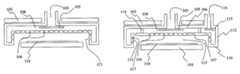
- FIG. 1is a prior art schematic diagram showing a typical showerhead.
- the showerheadconsists of the body structure 6 , enclosing an interior volume 8 .
- the precursorenters through the inlet port 3 , disperses in the interior volume 8 by the baffle 5 , and exits through the outlet ports 4 to the wafer 18 , sitting on top of the substrate 1 .
- the heater 2is used to maintain the showerhead at the desired temperature.
- the basic structure of the showerheadis the flat surface 7 in parallel to the substrate 1 .
- the precursor flow 20is in one direction only which is perpendicular to the flat surface 7 . A significant portion of the unreacted precursor is lost through the gap between the showerhead bottom surface 7 and the substrate 1 .
- Various designs of the showerheadexist in the literature, but all of them have a flat bottom surface containing the outlet ports, therefore significant precursor loss is inevitable.
- FIG. 2is another prior art schematic diagram described by Yong Ku Baek (U.S. Pat. No. 5,670,218) to focus the precursor onto the substrate.
- the showerheadhas a baffle guide 9 , surrounding the substrate 1 and the showerhead.
- This baffle guide 9serves to prevent the precursor from the showerhead from diffusing too widely or from leaking into a vacuum port too rapidly.
- This designhelps reduce precursor loss, but with the complexity of a separate baffle guide.
- uniform heating of the showerhead and the baffle guideis difficult or complex.
- Yong Ku Backhas not attempted to provide a heater element for his showerhead system. Also the precursor flow is in one direction only.
- Another important aspect of the process reactoris the heating of the reactor walls to prevent precursor condensation or moisture absorption.
- a CVD system or an etching systemis the heating of the reactor walls to prevent precursor condensation or moisture absorption.
- separate heated reactor wallsare needed to confine the showerhead and the substrate.
- the precursor flow from the showerheadhas more than one direction to further mixing of the precursor.
- a showerheadcould offer a vapor curtain wall to further confine the precursor inside the reaction zone.
- the three-dimensional showerheadcomprises an inverted-cup structure having double walls, an outer wall and an inner wall, said double walls defining a first interior volume and said inner wall defining an exterior cavity, said structure further having:
- first inlet portsconnected to said outer wall for introducing first process precursors into said first interior volume
- the inventionprovides a three-dimensional showerhead covering all directions except the direction covered by the substrate. Accordingly, the precursor vapor exiting from the showerhead will come from all directions except the direction covered by the substrate.
- the showerheadcould be made of metal such as stainless steel, aluminum, or anodized aluminum.
- the metal showerheadcould be used as an electrode in generating a plasma for the reactor.
- the showerheadcould also be made of insulated material such as ceramic.
- the showerheadcould also be made of transparent materials such as glass or quartz to permit the use of a lamp heating system.
- the outlet port dimensionranges from 0.2 mm to 2 mm in diameter.
- the outlet ports in the horizontal flat area of the showerheadare arranged in such a configuration as to provide uniform delivery of the precursor vapor to the flat portion of the substrate. Concentric circles, repeated polygons such as a hexagon, square, or triangle pattern are some examples of the outlet ports pattern.
- the outer ports in the vertical walls of the showerheadare arranged in such configuration to optimize the process film quality.
- the flowwill be horizontal with small openings to create a high velocity gas in the cavity.
- the flowwill be angled downward to minimize the turbulence in the cavity.
- the inlet portsare arranged in such configuration to maximize the uniformity of the precursor flow at the outlet. Examples of the configuration could be a single inlet port at the center of the showerhead, or 3 inlet ports arranged in a triangular pattern, or 4 inlet ports arranged in a square pattern.
- a heat transfer structureis included in the showerhead structure to controllably maintain the showerhead at the desired temperature level for efficient operation.
- a baffleis included in the inlet port to diffuse the precursor before exiting to the substrate.
- the three-dimensional showerheadhas outlet ports offering flow only in one direction.
- the side sections of the showerheadwill act only as a baffle to contain the precursor vapor. In some aspects of the invention, the side sections, since there is no precursor flowing from it, will be solid.
- the showerheadhas smoothed corners to minimize dead space.
- the two-zone showerheadcomprises a body structure having double walls, an outer wall and an inner wall, said double walls defining a first interior volume and said inner wall defining an exterior cavity, said structure further having:
- a partition walldividing the first interior volume into a first interior volume and a second interior volume
- first inlet portsconnected to said outer wall for introducing first precursors into said first interior volume
- the inventionprovides a two-zone showerhead with two separate inlets and two separate outlets.
- the two-zone three-dimensional showerheadcomprises an inverted-cup structure having double walls, an outer wall and an inner wall, said double walls defining a first interior volume and said inner wall defining an exterior cavity, said structure further having:
- a partition walldividing the first interior volume into a first interior volume and a second interior volume
- first inlet portsconnected to said outer wall for introducing first precursors into said first interior volume
- the inventionprovides a two-zone three-dimensional showerhead with two separate inlets and two separate outlets.
- the two-zone three-dimensional showerheadshares the two-zone feature with the two-zone showerhead and shares the three-dimensional feature with the three-dimensional showerhead.
- the central outlet portsprovide the active precursor vapor for the process and the outside outlet ports provide the purging gas needed to contain the active precursor.
- the flow of the outside portsis be horizontal with small openings to further contain the precursor within the reaction cavity. In some aspects of the invention, the flow of the outside ports is angled downward to minimize the turbulence in the cavity and further the purging action.
- the outlet port dimensionranges from 0.2 mm to 2 mm in diameter.
- the outlet ports in the horizontal flat area of the showerheadare arranged in such configuration as to have uniform delivery to the flat portion of the substrate. Concentric circles, repeated polygons such as a hexagon, square, or triangle pattern are some examples of the outlet ports pattern.
- the inlet portsare arranged in such configuration to maximize the uniformity of the precursor flow at the outlet. Example of the configuration could be a single inlet port at the center of the showerhead, or 3 inlet ports arranged in a triangular pattern, or 4 inlet ports arranged in a square pattern.
- a heat transfer structureis included in the showerhead structure to controllably maintain the showerhead at the desired temperature level to eliminate condensation of precursor vapors within the showerhead.
- a baffleis included in the inlet ports to diffuse the precursor before exiting to the substrate.
- the three-dimensional showerheadthere might not be a need for the reactor chamber body since the showerhead comprises a large portion of the chamber already. Therefore an application of the three-dimensional showerhead is the simplification of the reactor chamber. However, a complete reactor chamber could still be used to provide a cooler wall for safety purposes.
- Step aa further step precedes Step a), of heating the showerhead to the desired temperature.
- Step ba further step after Step b), of applying a power source to generate a plasma between the showerhead and the substrate.
- a two-zone showerheadis used.
- a two-zone three-dimensional showerheadis used.
- FIG. 1is a schematic of a prior art showerhead.
- FIG. 2is a schematic of a prior art showerhead with a baffle guide.
- FIG. 3depicts the present invention three-dimensional showerhead.
- FIG. 4shows the three-dimensional showerhead with a heat transfer structure and an inlet port baffle.
- FIG. 5shows a variation of the three-dimensional showerhead with smooth corners.
- FIG. 6shows a variation of the three-dimensional showerhead with one direction flow, together with a heat transfer structure and an inlet port baffle.
- FIG. 7shows the present invention two-zone showerhead with two zone inlet ports together with a heat transfer structure and inlet port baffles.
- FIG. 8shows the present invention two-zone three-dimensional showerhead with two zone inlet ports together with a heat transfer structure and inlet port baffles.
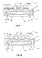
- FIG. 9shows a three-dimensional showerhead the 2 inlet ports.
- FIG. 10shows a variation of the three-dimensional showerhead with two zone inlet ports, having the second zone outlet ports facing downward.
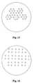
- FIG. 11shows a circular outlet port pattern
- FIG. 12shows a portion of a repeated hexagonal outlet port pattern.
- FIG. 13shows a portion of a repeated triangular outlet port pattern.
- FIG. 14shows a portion of a repeated square outlet port pattern.
- FIG. 3illustrates a three-dimensional showerhead according to one embodiment of the invention.
- the showerheadis composed of an inverted-cup body consisting of the top outer wall 106 , side outer wall 112 , bottom wall 110 , top inner wall 107 , and side inner wall 111 .
- Said inverted-cup bodydefines an interior volume 108 of the showerhead.
- the inverted-cupalso defines an exterior cavity 113 covered by the top inner wall 107 , and side inner wall 111 .
- the precursoris introduced into the interior volume 108 of the showerhead through the inlet port 103 , and exits to the external cavity 113 and onto the wafer 118 on top of the substrates support 101 .
- the gap 119 from the showerhead to the substrate support 101is also controllable to further confine the precursor inside the reaction zone.
- Pending patent application Ser. No. 09/169,819 “Manifold vaporization system and method” of the same inventorhas disclosed the method to improve the distribution of the precursor by using more than one inlet ports.
- Typical distribution of the multiple inlet portsis concentric circles or polygon patterns. With 3 inlet ports, the pattern is triangular. With 4 inlet ports, the pattern is square. With 7 inlet ports, the pattern is hexagonal with a center inlet port.
- the precursoris released to the exterior cavity 113 before reaching the wafer 118 through the vertical outlet ports 104 and the horizontal outlet ports 121 .
- This showerheadpermits precursor flow in the vertical direction 120 and the horizontal direction 122 .
- the outlet ports 104 and 121have a diameter small enough to ensure a pressure difference between the interior volume 108 and the exterior cavity 113 . This pressure difference will result in the evenly distributed precursor through the outlet ports.
- the outlet portsare typically perpendicular to the wall.
- the horizontal outlet ports 121 at the inner side wall 111are directed downward.
- the direction of the outlet ports 121 at the inner side wall 111is designed to optimize the processed film quality.
- the showerheadhas perpendicular outlet ports to the inner side wall 111 .
- the showerheadhas downward direction of the outlet ports at the inner side wall 111 .
- FIG. 4illustrates the three-dimensional showerhead with a heat transfer structure 102 and a baffle 105 . All other features are similar to the showerhead of FIG. 3 .
- the heat transfer structure 102serves to controllably maintain the showerhead at the desired temperature for efficient operation.
- Some precursors, especially the metal-organic precursors such as copper(hfac)L with Lis a ligand such as trimethylvinylsilane, tetrakisdimethylaminetitanium (TDMAT), tetrakisdiethylaminetitanium (TDEAT), pentadiethylaminetantalum (PDMAT), condense at room temperature. Therefore the showerhead is heated above room temperature to prevent condensation. Another purpose of the heated showerhead is to maintain a warm wall environment for desorption of condensable gases that could adversely affect the chemical reaction process.
- TDMATtetrakisdimethylaminetitanium
- TDEATtetrakisdiethylaminetit
- the showerheadfurther includes a baffle 105 to diffuse the precursor at the inlet port 103 , to prevent a high flow of the precursor exiting at the center of the showerhead.
- the baffle 105is also heated. The simplest form of heating is to get some heat transfer from the showerhead body. With proper design, the baffle 105 should achieve thermal equilibrium with the rest of the showerhead.
- FIG. 5shows a variation of the showerhead with smooth corners 123 .
- the smooth corners 123serve to minimize the dead space in the interior volume of the showerhead and the exterior cavity.
- the smooth cornersalso help minimize the high electric field concentration associated with sharp corners.
- FIG. 6illustrates a variation of the three-dimensional showerhead.
- the showerheadis composed of an inverted-cup body consisting of the top outer wall 106 , side top wall 112 , top inner wall 107 , and side bottom wall 121 .
- Said inverted-cup bodydefines an interior volume 108 of the showerhead.
- the inverted-cupalso defines an exterior cavity 113 covered by the top inner wall 107 , and side bottom wall 121 .
- the precursoris introduced into the interior volume 108 of the showerhead through the inlet port 103 , and exits to the external cavity 113 and onto the wafer 118 .
- the heat transfer structure 102serves to controllably maintain the showerhead to the desired temperature for efficient operation.
- Baffle 105serves to diffuse the precursor at the inlet port 103 , to prevent a high flow of the precursor exiting at the center of the showerhead. To prevent condensation, the baffle 105 is also heated. The outlet flow of this structure is only in one downward direction.
- FIG. 7illustrates the two-zone showerhead.
- the showerheadis composed of a flat body consisting of the top outer wall 106 , and bottom wall 107 . Together with divider 114 , the flat body defines an inner interior volume 108 and an outer interior volume 115 of the showerhead. The flat body also defines an exterior cavity 113 covered by the top inner wall 107 , and substrate support 101 .
- the first precursoris introduced into the inner interior volume 108 of the showerhead through the inlet port 103 , and exits to the external cavity 113 and onto the substrates support 101 .
- the second precursoris introduced into the outer interior volume 115 through the inlet port 116 , and exits to the external cavity 113 and onto the substrate support 101 .
- the heat transfer structure 102serves to controllably maintain the showerhead at the desired temperature for efficient operation.
- Baffle 105serves to diffuse the precursor at the inlet port 103 , to prevent a high flow of the precursor exiting at the center of the showerhead. To prevent condensation, the baffle 105 is also heated.
- the second outlet portsserve as a gas curtain.
- the second precursorconsists of non-reactive gas such as helium, nitrogen, argon to confine the precursor inside the reaction zone.
- FIG. 8illustrates the two-zone three-dimensional showerhead.
- the showerheadcomposes of an inverted-cup body consisting of the top outer wall 106 , side outer wall 112 , bottom wall 110 , top inner wall 107 , and side inner wall 111 .
- the inverted-cup bodydefines an inner interior volume 108 and an outer interior volume 115 of the showerhead.
- the inverted-cupalso defines an exterior cavity 113 covered by the top inner wall 107 , and side inner wall 111 .
- the first precursoris introduced into the inner interior volume 108 of the showerhead through the inlet port 103 , and exits to the external cavity 113 and onto the substrate support 101 .
- the second precursoris introduced into the outer interior volume 115 through the inlet port 116 , and exits to the external cavity 113 and onto the substrate support 101 .
- the heat transfer structure 102serves to controllably maintain the showerhead at the desired temperature for efficient operation.
- Baffle 105serves to diffuse the precursor at the inlet port 103 , to prevent a high flow of the precursor exiting at the center of the showerhead. To prevent condensation, the baffle 105 is also heated.
- the second precursoris a purge gas, serving to confine the first precursor inside the external cavity 113 .
- FIG. 9illustrates the two-zone three-dimensional showerhead with 2 inlet ports for the inner zone. Separate baffles serve to diffuse the precursor at each separate inlet port.
- FIG. 10illustrates another variation of the two-zone three-dimensional showerhead with 2 inlet ports for the inner zone.
- the second zone outlet ports 117are directed downward to confine the first precursor in the external cavity 113 and not interfere with the reaction of the first precursor.
- FIG. 11shows the concentric ring pattern of the outlet ports for the horizontal flat portion of the top inner wall 107 .
- the outlet ports diameterranges from 0.2 mm to 2 mm.
- the number of concentric ringranges from 5 to 40.
- FIG. 12shows the hexagonal pattern of the outlet ports.
- the diameter of the hexagonalranges from 5 mm to 20 mm.
- FIG. 13shows the triangular pattern of the outlet ports.
- the distance between 2 adjacent inlet portsranges from 2 mm to 15 mm.
- FIG. 14shows the square pattern of the outlet ports.
- the distance between 2 adjacent inlet portsranges from 2 mm to 15 mm.
Landscapes
- Chemical & Material Sciences (AREA)
- Engineering & Computer Science (AREA)
- General Chemical & Material Sciences (AREA)
- Chemical Kinetics & Catalysis (AREA)
- Materials Engineering (AREA)
- Mechanical Engineering (AREA)
- Metallurgy (AREA)
- Organic Chemistry (AREA)
- Physics & Mathematics (AREA)
- Condensed Matter Physics & Semiconductors (AREA)
- General Physics & Mathematics (AREA)
- Manufacturing & Machinery (AREA)
- Computer Hardware Design (AREA)
- Microelectronics & Electronic Packaging (AREA)
- Power Engineering (AREA)
- Chemical Vapour Deposition (AREA)
Abstract
Description
Claims (11)
Priority Applications (1)
| Application Number | Priority Date | Filing Date | Title |
|---|---|---|---|
| US09/520,108US6444039B1 (en) | 2000-03-07 | 2000-03-07 | Three-dimensional showerhead apparatus |
Applications Claiming Priority (1)
| Application Number | Priority Date | Filing Date | Title |
|---|---|---|---|
| US09/520,108US6444039B1 (en) | 2000-03-07 | 2000-03-07 | Three-dimensional showerhead apparatus |
Publications (1)
| Publication Number | Publication Date |
|---|---|
| US6444039B1true US6444039B1 (en) | 2002-09-03 |
Family
ID=24071231
Family Applications (1)
| Application Number | Title | Priority Date | Filing Date |
|---|---|---|---|
| US09/520,108Expired - LifetimeUS6444039B1 (en) | 2000-03-07 | 2000-03-07 | Three-dimensional showerhead apparatus |
Country Status (1)
| Country | Link |
|---|---|
| US (1) | US6444039B1 (en) |
Cited By (158)
| Publication number | Priority date | Publication date | Assignee | Title |
|---|---|---|---|---|
| US20020188376A1 (en)* | 2000-08-18 | 2002-12-12 | Micron Technology, Inc. | Preheating of chemical vapor deposition precursors |
| US20030037802A1 (en)* | 2001-07-23 | 2003-02-27 | Hitachi, Ltd. | Semiconductor treating apparatus and cleaning method of the same |
| US20030041971A1 (en)* | 2001-08-28 | 2003-03-06 | Nec Corporation | Substrate processing system for performing exposure process in gas atmosphere |
| US20030045060A1 (en)* | 2001-08-30 | 2003-03-06 | Micron Technology, Inc. | Crystalline or amorphous medium-k gate oxides, Y2O3 and Gd2O3 |
| US20030077388A1 (en)* | 2001-10-18 | 2003-04-24 | Chulsoo Byun | Method and apparatus for chemical vapor deposition capable of preventing contamination and enhancing film growth rate |
| US20030119246A1 (en)* | 2001-12-20 | 2003-06-26 | Micron Technology, Inc. | Low-temperature grown high quality ultra-thin CoTiO3 gate dielectrics |
| US6638880B2 (en)* | 1999-06-03 | 2003-10-28 | Mitsubishi Denki Kabushiki Kaisha | Chemical vapor deposition apparatus and a method of manufacturing a semiconductor device |
| US20030228747A1 (en)* | 2002-06-05 | 2003-12-11 | Micron Technology, Inc. | Pr2O3-based la-oxide gate dielectrics |
| US20030235066A1 (en)* | 2002-06-21 | 2003-12-25 | Micron Technology, Inc. | Ferroelectric write once read only memory for archival storage |
| US6678304B2 (en)* | 2000-08-22 | 2004-01-13 | Nec Corporation | Laser correction method and apparatus |
| US20040011292A1 (en)* | 2002-07-15 | 2004-01-22 | Akira Shimizu | Single-wafer-processing type CVD apparatus |
| US20040033681A1 (en)* | 2002-08-15 | 2004-02-19 | Micron Technology, Inc. | Lanthanide doped TiOx dielectric films by plasma oxidation |
| US20040038525A1 (en)* | 2002-08-26 | 2004-02-26 | Shuang Meng | Enhanced atomic layer deposition |
| US20040035358A1 (en)* | 2002-08-23 | 2004-02-26 | Cem Basceri | Reactors having gas distributors and methods for depositing materials onto micro-device workpieces |
| US20040060514A1 (en)* | 2002-01-25 | 2004-04-01 | Applied Materials, Inc. A Delaware Corporation | Gas distribution showerhead |
| US20040062862A1 (en)* | 2002-09-28 | 2004-04-01 | Ahn Seong Deok | Method and apparatus using large-area organic vapor deposition for formation of organic thin films or organic devices |
| US20040094092A1 (en)* | 2002-02-25 | 2004-05-20 | Derderian Garo J. | Apparatus for improved delivery of metastable species |
| US20040110391A1 (en)* | 2002-12-04 | 2004-06-10 | Micron Technology, Inc. | Atomic layer deposited Zr-Sn-Ti-O films |
| US20040110348A1 (en)* | 2002-12-04 | 2004-06-10 | Micron Technology, Inc. | Atomic layer deposited Zr-Sn-Ti-O films using TiI4 |
| US20040118519A1 (en)* | 2002-12-20 | 2004-06-24 | Applied Materials, Inc. | Blocker plate bypass design to improve clean rate at the edge of the chamber |
| US20040134611A1 (en)* | 2001-01-22 | 2004-07-15 | Tokyo Electron Limited | Plasma process system and plasma process method |
| US6767795B2 (en) | 2002-01-17 | 2004-07-27 | Micron Technology, Inc. | Highly reliable amorphous high-k gate dielectric ZrOXNY |
| US20040163765A1 (en)* | 2003-02-25 | 2004-08-26 | Ans Co., Ltd. | Plasma reactor for manufacturing electronic components |
| US20040173313A1 (en)* | 2003-03-03 | 2004-09-09 | Bradley Beach | Fire polished showerhead electrode |
| US6800139B1 (en)* | 1999-08-31 | 2004-10-05 | Tokyo Electron Limited | Film deposition apparatus and method |
| US20040194708A1 (en)* | 2001-01-22 | 2004-10-07 | Anelva Corporation | Method of cleaning a cvd device |
| US6812100B2 (en) | 2002-03-13 | 2004-11-02 | Micron Technology, Inc. | Evaporation of Y-Si-O films for medium-k dielectrics |
| US20040216671A1 (en)* | 2001-03-13 | 2004-11-04 | Carpenter Craig M | Chemical vapor deposition apparatuses |
| US20040235299A1 (en)* | 2003-05-22 | 2004-11-25 | Axcelis Technologies, Inc. | Plasma ashing apparatus and endpoint detection process |
| US20040238123A1 (en)* | 2003-05-22 | 2004-12-02 | Axcelis Technologies, Inc. | Plasma apparatus, gas distribution assembly for a plasma apparatus and processes therewith |
| US20050001556A1 (en)* | 2002-07-09 | 2005-01-06 | Applied Materials, Inc. | Capacitively coupled plasma reactor with magnetic plasma control |
| US20050011449A1 (en)* | 2002-10-31 | 2005-01-20 | Micron Technology, Inc. | Gas delivery system for deposition processes, and methods of using same |
| US20050019960A1 (en)* | 2003-07-25 | 2005-01-27 | Moon-Sook Lee | Method and apparatus for forming a ferroelectric layer |
| US6852167B2 (en)* | 2001-03-01 | 2005-02-08 | Micron Technology, Inc. | Methods, systems, and apparatus for uniform chemical-vapor depositions |
| US20050028732A1 (en)* | 2002-01-22 | 2005-02-10 | Mardian Allen P. | Chemical vapor deposition method |
| US20050032342A1 (en)* | 2002-08-22 | 2005-02-10 | Micron Technology, Inc. | Atomic layer deposition of CMOS gates with variable work functions |
| US20050109460A1 (en)* | 2003-05-30 | 2005-05-26 | Dedontney Jay B. | Adjustable gas distribution system |
| US20050134767A1 (en)* | 2003-12-20 | 2005-06-23 | Su-Seok Choi | Dual reflective liquid crystal display device |
| WO2005059974A1 (en)* | 2003-12-15 | 2005-06-30 | Applied Materials, Inc. | Edge flow faceplate for improvement of cvd film properties |
| US6921702B2 (en) | 2002-07-30 | 2005-07-26 | Micron Technology Inc. | Atomic layer deposited nanolaminates of HfO2/ZrO2 films as gate dielectrics |
| US20050183666A1 (en)* | 2004-02-20 | 2005-08-25 | Asm Japan K.K. | Shower plate having projections and plasma CVD apparatus using same |
| US20050191416A1 (en)* | 2002-08-15 | 2005-09-01 | Cem Basceri | Methods of gas delivery for deposition processes and methods of depositing material on a substrate |
| US20050233477A1 (en)* | 2004-03-05 | 2005-10-20 | Tokyo Electron Limited | Substrate processing apparatus, substrate processing method, and program for implementing the method |
| US20050241579A1 (en)* | 2004-04-30 | 2005-11-03 | Russell Kidd | Face shield to improve uniformity of blanket CVD processes |
| US20050242061A1 (en)* | 2001-11-27 | 2005-11-03 | Hideaki Fukuda | Self-cleaning method for plasma CVD apparatus |
| WO2005069344A3 (en)* | 2004-01-12 | 2005-11-24 | Axcelis Tech Inc | Gas distribution plate assembly for plasma reactors |
| US20050263248A1 (en)* | 2004-05-26 | 2005-12-01 | Applied Materials, Inc. | Blocker plate bypass to distribute gases in a chemical vapor deposition system |
| US20050263072A1 (en)* | 2004-05-26 | 2005-12-01 | Applied Materials, Inc. | Uniformity control for low flow process and chamber to chamber matching |
| US20050277289A1 (en)* | 2003-11-12 | 2005-12-15 | Eric Wagganer | Line edge roughness reduction for trench etch |
| US20060001848A1 (en)* | 2004-06-30 | 2006-01-05 | Lg Philips Lcd Co., Ltd. | Apparatus for fabricating semiconductor device |
| US20060046520A1 (en)* | 2004-09-01 | 2006-03-02 | Applied Materials, Inc. | Method to deposit functionally graded dielectric films via chemical vapor deposition using viscous precursors |
| US7056806B2 (en) | 2003-09-17 | 2006-06-06 | Micron Technology, Inc. | Microfeature workpiece processing apparatus and methods for controlling deposition of materials on microfeature workpieces |
| US20060196603A1 (en)* | 2005-03-07 | 2006-09-07 | Applied Materials, Inc. | Gas baffle and distributor for semiconductor processing chamber |
| US20060240626A1 (en)* | 2002-06-21 | 2006-10-26 | Micron Technology, Inc. | Write once read only memory employing charge trapping in insulators |
| US7130220B2 (en) | 2002-06-21 | 2006-10-31 | Micron Technology, Inc. | Write once read only memory employing floating gates |
| US7135421B2 (en) | 2002-06-05 | 2006-11-14 | Micron Technology, Inc. | Atomic layer-deposited hafnium aluminum oxide |
| US7160577B2 (en) | 2002-05-02 | 2007-01-09 | Micron Technology, Inc. | Methods for atomic-layer deposition of aluminum oxides in integrated circuits |
| US7166509B2 (en) | 2002-06-21 | 2007-01-23 | Micron Technology, Inc. | Write once read only memory with large work function floating gates |
| US7199023B2 (en) | 2002-08-28 | 2007-04-03 | Micron Technology, Inc. | Atomic layer deposited HfSiON dielectric films wherein each precursor is independendently pulsed |
| US7235138B2 (en) | 2003-08-21 | 2007-06-26 | Micron Technology, Inc. | Microfeature workpiece processing apparatus and methods for batch deposition of materials on microfeature workpieces |
| US7258892B2 (en) | 2003-12-10 | 2007-08-21 | Micron Technology, Inc. | Methods and systems for controlling temperature during microfeature workpiece processing, e.g., CVD deposition |
| US7259434B2 (en) | 2001-08-30 | 2007-08-21 | Micron Technology, Inc. | Highly reliable amorphous high-k gate oxide ZrO2 |
| US20070209686A1 (en)* | 2006-03-07 | 2007-09-13 | Atto Co., Ltd. | Apparatus for cleaning chamber using gas separation type showerhead |
| US20070235137A1 (en)* | 2006-03-28 | 2007-10-11 | Tokyo Electon Limited | Gas distribution system for a post-etch treatment system |
| US7282239B2 (en) | 2003-09-18 | 2007-10-16 | Micron Technology, Inc. | Systems and methods for depositing material onto microfeature workpieces in reaction chambers |
| US7323231B2 (en) | 2003-10-09 | 2008-01-29 | Micron Technology, Inc. | Apparatus and methods for plasma vapor deposition processes |
| US7335396B2 (en) | 2003-04-24 | 2008-02-26 | Micron Technology, Inc. | Methods for controlling mass flow rates and pressures in passageways coupled to reaction chambers and systems for depositing material onto microfeature workpieces in reaction chambers |
| US7344755B2 (en) | 2003-08-21 | 2008-03-18 | Micron Technology, Inc. | Methods and apparatus for processing microfeature workpieces; methods for conditioning ALD reaction chambers |
| US20080078746A1 (en)* | 2006-08-15 | 2008-04-03 | Noriiki Masuda | Substrate processing system, gas supply unit, method of substrate processing, computer program, and storage medium |
| US20080099147A1 (en)* | 2006-10-26 | 2008-05-01 | Nyi Oo Myo | Temperature controlled multi-gas distribution assembly |
| US20080121178A1 (en)* | 2006-11-28 | 2008-05-29 | Applied Materials, Inc. | Dual top gas feed through distributor for high density plasma chamber |
| US20080121179A1 (en)* | 2006-11-28 | 2008-05-29 | Applied Materials, Inc. | Gas baffle and distributor for semiconductor processing chamber |
| US20080121177A1 (en)* | 2006-11-28 | 2008-05-29 | Applied Materials, Inc. | Dual top gas feed through distributor for high density plasma chamber |
| US7387685B2 (en) | 2002-07-08 | 2008-06-17 | Micron Technology, Inc. | Apparatus and method for depositing materials onto microelectronic workpieces |
| US20080178914A1 (en)* | 2007-01-26 | 2008-07-31 | Tokyo Electron Limited | Substrate processing apparatus |
| US7422635B2 (en) | 2003-08-28 | 2008-09-09 | Micron Technology, Inc. | Methods and apparatus for processing microfeature workpieces, e.g., for depositing materials on microfeature workpieces |
| US20080223523A1 (en)* | 2007-03-12 | 2008-09-18 | Tokyo Electron Limited | Substrate processing apparatus and electrode structure |
| US7431967B2 (en) | 2002-09-19 | 2008-10-07 | Applied Materials, Inc. | Limited thermal budget formation of PMD layers |
| US7456116B2 (en) | 2002-09-19 | 2008-11-25 | Applied Materials, Inc. | Gap-fill depositions in the formation of silicon containing dielectric materials |
| US7468104B2 (en)* | 2002-05-17 | 2008-12-23 | Micron Technology, Inc. | Chemical vapor deposition apparatus and deposition method |
| US7481887B2 (en) | 2002-05-24 | 2009-01-27 | Micron Technology, Inc. | Apparatus for controlling gas pulsing in processes for depositing materials onto micro-device workpieces |
| US20090061646A1 (en)* | 2007-09-05 | 2009-03-05 | Chiang Tony P | Vapor based combinatorial processing |
| US20090093129A1 (en)* | 2006-11-28 | 2009-04-09 | Applied Materials, Inc. | Gas Baffle and Distributor for Semiconductor Processing Chamber |
| US20090095221A1 (en)* | 2007-10-16 | 2009-04-16 | Alexander Tam | Multi-gas concentric injection showerhead |
| US20090117746A1 (en)* | 2007-11-02 | 2009-05-07 | Tokyo Electron Limited | Gas supply device, substrate processing apparatus and substrate processing method |
| US7560793B2 (en) | 2002-05-02 | 2009-07-14 | Micron Technology, Inc. | Atomic layer deposition and conversion |
| US7563730B2 (en) | 2006-08-31 | 2009-07-21 | Micron Technology, Inc. | Hafnium lanthanide oxynitride films |
| US7581511B2 (en) | 2003-10-10 | 2009-09-01 | Micron Technology, Inc. | Apparatus and methods for manufacturing microfeatures on workpieces using plasma vapor processes |
| US7584942B2 (en) | 2004-03-31 | 2009-09-08 | Micron Technology, Inc. | Ampoules for producing a reaction gas and systems for depositing materials onto microfeature workpieces in reaction chambers |
| US7588804B2 (en) | 2002-08-15 | 2009-09-15 | Micron Technology, Inc. | Reactors with isolated gas connectors and methods for depositing materials onto micro-device workpieces |
| US20090246374A1 (en)* | 2008-03-28 | 2009-10-01 | Tokyo Electron Limited | Gas distribution system and method for distributing process gas in a processing system |
| US20090275210A1 (en)* | 2008-05-02 | 2009-11-05 | Sunil Shanker | Combinatorial plasma enhanced deposition techniques |
| US7615061B2 (en) | 2006-02-28 | 2009-11-10 | Arthrocare Corporation | Bone anchor suture-loading system, method and apparatus |
| US7642171B2 (en) | 2004-08-04 | 2010-01-05 | Applied Materials, Inc. | Multi-step anneal of thin films for film densification and improved gap-fill |
| US7647886B2 (en) | 2003-10-15 | 2010-01-19 | Micron Technology, Inc. | Systems for depositing material onto workpieces in reaction chambers and methods for removing byproducts from reaction chambers |
| US7662729B2 (en) | 2005-04-28 | 2010-02-16 | Micron Technology, Inc. | Atomic layer deposition of a ruthenium layer to a lanthanide oxide dielectric layer |
| US7674727B2 (en) | 2002-09-19 | 2010-03-09 | Applied Materials, Inc. | Nitrous oxide anneal of TEOS/ozone CVD for improved gapfill |
| US7687848B2 (en) | 2002-07-08 | 2010-03-30 | Micron Technology, Inc. | Memory utilizing oxide-conductor nanolaminates |
| US7687409B2 (en) | 2005-03-29 | 2010-03-30 | Micron Technology, Inc. | Atomic layer deposited titanium silicon oxide films |
| US7699932B2 (en)* | 2004-06-02 | 2010-04-20 | Micron Technology, Inc. | Reactors, systems and methods for depositing thin films onto microfeature workpieces |
| US7709402B2 (en) | 2006-02-16 | 2010-05-04 | Micron Technology, Inc. | Conductive layers for hafnium silicon oxynitride films |
| US7728626B2 (en) | 2002-07-08 | 2010-06-01 | Micron Technology, Inc. | Memory utilizing oxide nanolaminates |
| US20100279008A1 (en)* | 2007-09-12 | 2010-11-04 | Tokyo Electron Limited | Film deposition apparatus and film deposition method |
| US7869242B2 (en) | 1999-07-30 | 2011-01-11 | Micron Technology, Inc. | Transmission lines for CMOS integrated circuits |
| US7906393B2 (en) | 2004-01-28 | 2011-03-15 | Micron Technology, Inc. | Methods for forming small-scale capacitor structures |
| US20110226181A1 (en)* | 2010-03-16 | 2011-09-22 | Tokyo Electron Limited | Film forming apparatus |
| US20110256315A1 (en)* | 2010-04-14 | 2011-10-20 | Applied Materials, Inc. | Showerhead assembly with gas injection distribution devices |
| US8048806B2 (en) | 2000-03-17 | 2011-11-01 | Applied Materials, Inc. | Methods to avoid unstable plasma states during a process transition |
| EP2304774A4 (en)* | 2008-07-03 | 2012-02-29 | Applied Materials Inc | Apparatuses for atomic layer deposition |
| US20120052216A1 (en)* | 2010-08-27 | 2012-03-01 | Applied Materials, Inc. | Gas distribution showerhead with high emissivity surface |
| US8133554B2 (en) | 2004-05-06 | 2012-03-13 | Micron Technology, Inc. | Methods for depositing material onto microfeature workpieces in reaction chambers and systems for depositing materials onto microfeature workpieces |
| US8143147B1 (en) | 2011-02-10 | 2012-03-27 | Intermolecular, Inc. | Methods and systems for forming thin films |
| US20120180725A1 (en)* | 2011-01-17 | 2012-07-19 | Furukawa Electric Co., Ltd. | Cvd apparatus |
| US20130180452A1 (en)* | 2012-01-18 | 2013-07-18 | Tokyo Electron Limited | Film deposition apparatus |
| US8501563B2 (en) | 2005-07-20 | 2013-08-06 | Micron Technology, Inc. | Devices with nanocrystals and methods of formation |
| US20130199729A1 (en)* | 2008-03-06 | 2013-08-08 | Tokyo Electron Limited | Processing gas diffusing and supplying unit and substrate procesisng apparatus |
| EP2638972A1 (en)* | 2012-03-12 | 2013-09-18 | Kohler Co. | Faceplate for shower device |
| JP2013541182A (en)* | 2010-08-16 | 2013-11-07 | アプライド マテリアルズ インコーポレイテッド | Shower head assembly with gas injection and dispersion device |
| US8580670B2 (en) | 2009-02-11 | 2013-11-12 | Kenneth Scott Alexander Butcher | Migration and plasma enhanced chemical vapor deposition |
| US8617351B2 (en) | 2002-07-09 | 2013-12-31 | Applied Materials, Inc. | Plasma reactor with minimal D.C. coils for cusp, solenoid and mirror fields for plasma uniformity and device damage reduction |
| US20140083612A1 (en)* | 2012-09-24 | 2014-03-27 | Psk Inc. | Baffle and method for treating surface of the baffle, and substrate treating apparatus and method for treating surface of the apparatus |
| USD707329S1 (en) | 2012-03-12 | 2014-06-17 | Kohler Co. | Shower faceplate |
| US20140217193A1 (en)* | 2013-02-06 | 2014-08-07 | Novellus Systems, Inc. | Method and apparatus for purging and plasma suppression in a process chamber |
| USD715398S1 (en) | 2013-03-16 | 2014-10-14 | Kohler Co. | Shower faceplate |
| USD715896S1 (en) | 2013-03-15 | 2014-10-21 | Kohler Co. | Shower faceplate |
| USD716415S1 (en) | 2013-03-15 | 2014-10-28 | Kohler Co. | Shower faceplate |
| USD719240S1 (en) | 2013-08-23 | 2014-12-09 | Kohler Co. | Shower device |
| US20150047567A1 (en)* | 2012-03-30 | 2015-02-19 | Tokyo Electron Limited | Film-forming apparatus |
| US9018108B2 (en) | 2013-01-25 | 2015-04-28 | Applied Materials, Inc. | Low shrinkage dielectric films |
| US20150167168A1 (en)* | 2013-12-18 | 2015-06-18 | Lam Research Corporation | Semiconductor substrate processing apparatus including uniformity baffles |
| US9129778B2 (en) | 2011-03-18 | 2015-09-08 | Lam Research Corporation | Fluid distribution members and/or assemblies |
| USD740917S1 (en) | 2013-03-16 | 2015-10-13 | Kohler Co. | Shower faceplate for shower device |
| US9177839B2 (en) | 2008-03-06 | 2015-11-03 | Tokyo Electron Limited | Cover part, process gas diffusing and supplying unit, and substrate processing apparatus |
| US20150315706A1 (en)* | 2014-05-05 | 2015-11-05 | Lam Research Corporation | Low volume showerhead with porous baffle |
| US20160177445A1 (en)* | 2014-12-22 | 2016-06-23 | Tokyo Electron Limited | Film forming apparatus |
| US20160177442A1 (en)* | 2014-12-18 | 2016-06-23 | Ervin Beloni | Gas shield for vapor deposition |
| US9687859B2 (en) | 2012-11-16 | 2017-06-27 | Kohler Co. | Shower device |
| US9758868B1 (en) | 2016-03-10 | 2017-09-12 | Lam Research Corporation | Plasma suppression behind a showerhead through the use of increased pressure |
| US20170268711A1 (en)* | 2016-03-15 | 2017-09-21 | Kabushiki Kaisha Toshiba | Branching structure |
| US9835388B2 (en) | 2012-01-06 | 2017-12-05 | Novellus Systems, Inc. | Systems for uniform heat transfer including adaptive portions |
| US10023959B2 (en) | 2015-05-26 | 2018-07-17 | Lam Research Corporation | Anti-transient showerhead |
| US10221484B2 (en) | 2007-10-16 | 2019-03-05 | Novellus Systems, Inc. | Temperature controlled showerhead |
| US10287683B2 (en) | 2012-06-25 | 2019-05-14 | Lam Research Corporation | Suppression of parasitic deposition in a substrate processing system by suppressing precursor flow and plasma outside of substrate region |
| WO2019113478A1 (en)* | 2017-12-08 | 2019-06-13 | Lam Research Corporation | Integrated showerhead with improved hole pattern for delivering radical and precursor gas to a downstream chamber to enable remote plasma film deposition |
| US10347547B2 (en) | 2016-08-09 | 2019-07-09 | Lam Research Corporation | Suppressing interfacial reactions by varying the wafer temperature throughout deposition |
| US10378107B2 (en) | 2015-05-22 | 2019-08-13 | Lam Research Corporation | Low volume showerhead with faceplate holes for improved flow uniformity |
| US10400333B2 (en) | 2011-03-04 | 2019-09-03 | Novellus Systems, Inc. | Hybrid ceramic showerhead |
| CN110400764A (en)* | 2018-04-25 | 2019-11-01 | 三星电子株式会社 | Gas injector and wafer processing equipment having the same |
| CN110656317A (en)* | 2019-09-19 | 2020-01-07 | 长江存储科技有限责任公司 | Shower head assembly, deposition apparatus and deposition method |
| US10541145B2 (en)* | 2017-03-29 | 2020-01-21 | Tokyo Electron Limited | Substrate processing apparatus and substrate processing method |
| US11182518B2 (en)* | 2018-01-24 | 2021-11-23 | Samsung Electronics Co., Ltd. | Apparatus and method for designing and manufacturing showerhead |
| US20220037577A1 (en)* | 2019-02-25 | 2022-02-03 | Corning Incorporated | Multi-showerhead chemical vapor deposition reactor, process and products |
| US11466365B2 (en)* | 2018-07-06 | 2022-10-11 | Tokyo Electron Limited | Film-forming apparatus |
| US11608559B2 (en) | 2016-12-14 | 2023-03-21 | Lam Research Corporation | Integrated showerhead with thermal control for delivering radical and precursor gas to a downstream chamber to enable remote plasma film deposition |
| JP2023048154A (en)* | 2021-09-27 | 2023-04-06 | ユ-ジーン テクノロジー カンパニー.リミテッド | Shower head and substrate processing equipment |
| US12087573B2 (en) | 2019-07-17 | 2024-09-10 | Lam Research Corporation | Modulation of oxidation profile for substrate processing |
| US12203168B2 (en) | 2019-08-28 | 2025-01-21 | Lam Research Corporation | Metal deposition |
| JP2025079672A (en)* | 2023-11-10 | 2025-05-22 | ヴイエム インコーポレイテッド | Shallow Etch Process Chamber |
Citations (19)
| Publication number | Priority date | Publication date | Assignee | Title |
|---|---|---|---|---|
| JPS55166926A (en)* | 1979-06-15 | 1980-12-26 | Pioneer Electronic Corp | Dry etching apparatus |
| JPS60189928A (en)* | 1984-03-12 | 1985-09-27 | Fujitsu Ltd | Vapor growth device under reduced pressure |
| JPS615515A (en)* | 1984-06-07 | 1986-01-11 | Fujitsu Ltd | Chemical vapor growth apparatus |
| JPS6179773A (en)* | 1984-09-27 | 1986-04-23 | Fujitsu Ltd | CVD equipment |
| US4820371A (en)* | 1987-12-15 | 1989-04-11 | Texas Instruments Incorporated | Apertured ring for exhausting plasma reactor gases |
| US4993358A (en)* | 1989-07-28 | 1991-02-19 | Watkins-Johnson Company | Chemical vapor deposition reactor and method of operation |
| US5106453A (en)* | 1990-01-29 | 1992-04-21 | At&T Bell Laboratories | MOCVD method and apparatus |
| US5532190A (en)* | 1994-05-26 | 1996-07-02 | U.S. Philips Corporation | Plasma treatment method in electronic device manufacture |
| US5552017A (en)* | 1995-11-27 | 1996-09-03 | Taiwan Semiconductor Manufacturing Company | Method for improving the process uniformity in a reactor by asymmetrically adjusting the reactant gas flow |
| US5614026A (en) | 1996-03-29 | 1997-03-25 | Lam Research Corporation | Showerhead for uniform distribution of process gas |
| US5624498A (en) | 1993-12-22 | 1997-04-29 | Samsung Electronics Co., Ltd. | Showerhead for a gas supplying apparatus |
| US5670218A (en) | 1995-10-04 | 1997-09-23 | Hyundai Electronics Industries Co., Ltd. | Method for forming ferroelectric thin film and apparatus therefor |
| JPH1064831A (en)* | 1996-08-20 | 1998-03-06 | Fujitsu Ltd | Vapor phase growth equipment |
| US5741363A (en) | 1996-03-22 | 1998-04-21 | Advanced Technology Materials, Inc. | Interiorly partitioned vapor injector for delivery of source reagent vapor mixtures for chemical vapor deposition |
| US5954887A (en)* | 1997-06-21 | 1999-09-21 | Tokyo Electron Limited | Cleaning processing method of a film forming apparatus |
| JPH11279778A (en)* | 1998-03-30 | 1999-10-12 | Seiko Epson Corp | Etching apparatus and method for manufacturing semiconductor device |
| US6050506A (en)* | 1998-02-13 | 2000-04-18 | Applied Materials, Inc. | Pattern of apertures in a showerhead for chemical vapor deposition |
| US6059885A (en)* | 1996-12-19 | 2000-05-09 | Toshiba Ceramics Co., Ltd. | Vapor deposition apparatus and method for forming thin film |
| US6265311B1 (en)* | 1999-04-27 | 2001-07-24 | Tokyo Electron Limited | PECVD of TaN films from tantalum halide precursors |
- 2000
- 2000-03-07USUS09/520,108patent/US6444039B1/ennot_activeExpired - Lifetime
Patent Citations (19)
| Publication number | Priority date | Publication date | Assignee | Title |
|---|---|---|---|---|
| JPS55166926A (en)* | 1979-06-15 | 1980-12-26 | Pioneer Electronic Corp | Dry etching apparatus |
| JPS60189928A (en)* | 1984-03-12 | 1985-09-27 | Fujitsu Ltd | Vapor growth device under reduced pressure |
| JPS615515A (en)* | 1984-06-07 | 1986-01-11 | Fujitsu Ltd | Chemical vapor growth apparatus |
| JPS6179773A (en)* | 1984-09-27 | 1986-04-23 | Fujitsu Ltd | CVD equipment |
| US4820371A (en)* | 1987-12-15 | 1989-04-11 | Texas Instruments Incorporated | Apertured ring for exhausting plasma reactor gases |
| US4993358A (en)* | 1989-07-28 | 1991-02-19 | Watkins-Johnson Company | Chemical vapor deposition reactor and method of operation |
| US5106453A (en)* | 1990-01-29 | 1992-04-21 | At&T Bell Laboratories | MOCVD method and apparatus |
| US5624498A (en) | 1993-12-22 | 1997-04-29 | Samsung Electronics Co., Ltd. | Showerhead for a gas supplying apparatus |
| US5532190A (en)* | 1994-05-26 | 1996-07-02 | U.S. Philips Corporation | Plasma treatment method in electronic device manufacture |
| US5670218A (en) | 1995-10-04 | 1997-09-23 | Hyundai Electronics Industries Co., Ltd. | Method for forming ferroelectric thin film and apparatus therefor |
| US5552017A (en)* | 1995-11-27 | 1996-09-03 | Taiwan Semiconductor Manufacturing Company | Method for improving the process uniformity in a reactor by asymmetrically adjusting the reactant gas flow |
| US5741363A (en) | 1996-03-22 | 1998-04-21 | Advanced Technology Materials, Inc. | Interiorly partitioned vapor injector for delivery of source reagent vapor mixtures for chemical vapor deposition |
| US5614026A (en) | 1996-03-29 | 1997-03-25 | Lam Research Corporation | Showerhead for uniform distribution of process gas |
| JPH1064831A (en)* | 1996-08-20 | 1998-03-06 | Fujitsu Ltd | Vapor phase growth equipment |
| US6059885A (en)* | 1996-12-19 | 2000-05-09 | Toshiba Ceramics Co., Ltd. | Vapor deposition apparatus and method for forming thin film |
| US5954887A (en)* | 1997-06-21 | 1999-09-21 | Tokyo Electron Limited | Cleaning processing method of a film forming apparatus |
| US6050506A (en)* | 1998-02-13 | 2000-04-18 | Applied Materials, Inc. | Pattern of apertures in a showerhead for chemical vapor deposition |
| JPH11279778A (en)* | 1998-03-30 | 1999-10-12 | Seiko Epson Corp | Etching apparatus and method for manufacturing semiconductor device |
| US6265311B1 (en)* | 1999-04-27 | 2001-07-24 | Tokyo Electron Limited | PECVD of TaN films from tantalum halide precursors |
Non-Patent Citations (1)
| Title |
|---|
| Bui, V.Q. Et Al, Etch Gas Distribution Manifold for Plasma Reactor, Sep. 1984, IBM Technical Disclosure Bulletin, vol. 27, No. 4A, P. 1978.* |
Cited By (324)
| Publication number | Priority date | Publication date | Assignee | Title |
|---|---|---|---|---|
| US6638880B2 (en)* | 1999-06-03 | 2003-10-28 | Mitsubishi Denki Kabushiki Kaisha | Chemical vapor deposition apparatus and a method of manufacturing a semiconductor device |
| US7869242B2 (en) | 1999-07-30 | 2011-01-11 | Micron Technology, Inc. | Transmission lines for CMOS integrated circuits |
| US6800139B1 (en)* | 1999-08-31 | 2004-10-05 | Tokyo Electron Limited | Film deposition apparatus and method |
| US8048806B2 (en) | 2000-03-17 | 2011-11-01 | Applied Materials, Inc. | Methods to avoid unstable plasma states during a process transition |
| US20050158997A1 (en)* | 2000-08-18 | 2005-07-21 | Micron Technology, Inc. | Preheating of chemical vapor deposition precursors |
| US20020188376A1 (en)* | 2000-08-18 | 2002-12-12 | Micron Technology, Inc. | Preheating of chemical vapor deposition precursors |
| US7204885B2 (en)* | 2000-08-18 | 2007-04-17 | Micron Technology, Inc. | Deposition system to provide preheating of chemical vapor deposition precursors |
| US20020195710A1 (en)* | 2000-08-18 | 2002-12-26 | Micron Technology, Inc. | Preheating of chemical vapor deposition precursors |
| US20030032283A1 (en)* | 2000-08-18 | 2003-02-13 | Micron Technology, Inc. | Preheating of chemical vapor deposition precursors |
| US7105441B2 (en) | 2000-08-18 | 2006-09-12 | Micron Technology, Inc. | Preheating of chemical vapor deposition precursors |
| US6678304B2 (en)* | 2000-08-22 | 2004-01-13 | Nec Corporation | Laser correction method and apparatus |
| US20040194708A1 (en)* | 2001-01-22 | 2004-10-07 | Anelva Corporation | Method of cleaning a cvd device |
| US20040134611A1 (en)* | 2001-01-22 | 2004-07-15 | Tokyo Electron Limited | Plasma process system and plasma process method |
| US20080276957A1 (en)* | 2001-01-22 | 2008-11-13 | Anelva Corporation | Method of cleaning a cvd device |
| US7481886B2 (en)* | 2001-01-22 | 2009-01-27 | Tokyo Electron Limited | Plasma process system and plasma process method |
| US8105440B2 (en) | 2001-01-22 | 2012-01-31 | Canon Anelva Corporation | Method of cleaning a CVD device |
| US7410668B2 (en) | 2001-03-01 | 2008-08-12 | Micron Technology, Inc. | Methods, systems, and apparatus for uniform chemical-vapor depositions |
| US6852167B2 (en)* | 2001-03-01 | 2005-02-08 | Micron Technology, Inc. | Methods, systems, and apparatus for uniform chemical-vapor depositions |
| US7378127B2 (en) | 2001-03-13 | 2008-05-27 | Micron Technology, Inc. | Chemical vapor deposition methods |
| US20040216671A1 (en)* | 2001-03-13 | 2004-11-04 | Carpenter Craig M | Chemical vapor deposition apparatuses |
| US20030037802A1 (en)* | 2001-07-23 | 2003-02-27 | Hitachi, Ltd. | Semiconductor treating apparatus and cleaning method of the same |
| US20090263974A1 (en)* | 2001-08-28 | 2009-10-22 | Shusaku Kido | Substrate processing system for performing exposure process in gas atmosphere |
| US20030041971A1 (en)* | 2001-08-28 | 2003-03-06 | Nec Corporation | Substrate processing system for performing exposure process in gas atmosphere |
| US20080121173A1 (en)* | 2001-08-28 | 2008-05-29 | Shusaku Kido | Substrate processing system for performing exposure process in gas atmosphere |
| US20030045060A1 (en)* | 2001-08-30 | 2003-03-06 | Micron Technology, Inc. | Crystalline or amorphous medium-k gate oxides, Y2O3 and Gd2O3 |
| US7208804B2 (en) | 2001-08-30 | 2007-04-24 | Micron Technology, Inc. | Crystalline or amorphous medium-K gate oxides, Y203 and Gd203 |
| US8026161B2 (en) | 2001-08-30 | 2011-09-27 | Micron Technology, Inc. | Highly reliable amorphous high-K gate oxide ZrO2 |
| US8652957B2 (en) | 2001-08-30 | 2014-02-18 | Micron Technology, Inc. | High-K gate dielectric oxide |
| US6844203B2 (en) | 2001-08-30 | 2005-01-18 | Micron Technology, Inc. | Gate oxides, and methods of forming |
| US7259434B2 (en) | 2001-08-30 | 2007-08-21 | Micron Technology, Inc. | Highly reliable amorphous high-k gate oxide ZrO2 |
| US20030077388A1 (en)* | 2001-10-18 | 2003-04-24 | Chulsoo Byun | Method and apparatus for chemical vapor deposition capable of preventing contamination and enhancing film growth rate |
| US7485339B2 (en) | 2001-10-18 | 2009-02-03 | Chulsoo Byun | Method for chemical vapor deposition capable of preventing contamination and enhancing film growth rate |
| US20070065599A1 (en)* | 2001-10-18 | 2007-03-22 | Chulsoo Byun | Method and apparatus for chemical vapor deposition capable of preventing contamination and enhancing film growth rate |
| US7156921B2 (en)* | 2001-10-18 | 2007-01-02 | Chulsoo Byun | Method and apparatus for chemical vapor deposition capable of preventing contamination and enhancing film growth rate |
| US20050242061A1 (en)* | 2001-11-27 | 2005-11-03 | Hideaki Fukuda | Self-cleaning method for plasma CVD apparatus |
| US7429515B2 (en) | 2001-12-20 | 2008-09-30 | Micron Technology, Inc. | Low-temperature grown high quality ultra-thin CoTiO3 gate dielectrics |
| US8178413B2 (en) | 2001-12-20 | 2012-05-15 | Micron Technology, Inc. | Low-temperature grown high quality ultra-thin CoTiO3 gate dielectrics |
| US20030119246A1 (en)* | 2001-12-20 | 2003-06-26 | Micron Technology, Inc. | Low-temperature grown high quality ultra-thin CoTiO3 gate dielectrics |
| US7804144B2 (en) | 2001-12-20 | 2010-09-28 | Micron Technology, Inc. | Low-temperature grown high quality ultra-thin CoTiO3 gate dielectrics |
| US6953730B2 (en) | 2001-12-20 | 2005-10-11 | Micron Technology, Inc. | Low-temperature grown high quality ultra-thin CoTiO3 gate dielectrics |
| US7205620B2 (en) | 2002-01-17 | 2007-04-17 | Micron Technology, Inc. | Highly reliable amorphous high-k gate dielectric ZrOxNy |
| US6767795B2 (en) | 2002-01-17 | 2004-07-27 | Micron Technology, Inc. | Highly reliable amorphous high-k gate dielectric ZrOXNY |
| US20050028732A1 (en)* | 2002-01-22 | 2005-02-10 | Mardian Allen P. | Chemical vapor deposition method |
| US7229666B2 (en) | 2002-01-22 | 2007-06-12 | Micron Technology, Inc. | Chemical vapor deposition method |
| US20040060514A1 (en)* | 2002-01-25 | 2004-04-01 | Applied Materials, Inc. A Delaware Corporation | Gas distribution showerhead |
| US7393562B2 (en) | 2002-02-25 | 2008-07-01 | Micron Technology, Inc. | Deposition methods for improved delivery of metastable species |
| US20040213908A1 (en)* | 2002-02-25 | 2004-10-28 | Derderian Garo J. | Deposition methods and apparatus for improved delivery of metastable species |
| US20040094092A1 (en)* | 2002-02-25 | 2004-05-20 | Derderian Garo J. | Apparatus for improved delivery of metastable species |
| US7527693B2 (en) | 2002-02-25 | 2009-05-05 | Micron Technology, Inc. | Apparatus for improved delivery of metastable species |
| US6812100B2 (en) | 2002-03-13 | 2004-11-02 | Micron Technology, Inc. | Evaporation of Y-Si-O films for medium-k dielectrics |
| US6930346B2 (en) | 2002-03-13 | 2005-08-16 | Micron Technology, Inc. | Evaporation of Y-Si-O films for medium-K dielectrics |
| US20050026374A1 (en)* | 2002-03-13 | 2005-02-03 | Micron Technology, Inc. | Evaporation of Y-Si-O films for medium-K dielectrics |
| US7160577B2 (en) | 2002-05-02 | 2007-01-09 | Micron Technology, Inc. | Methods for atomic-layer deposition of aluminum oxides in integrated circuits |
| US7560793B2 (en) | 2002-05-02 | 2009-07-14 | Micron Technology, Inc. | Atomic layer deposition and conversion |
| US7589029B2 (en) | 2002-05-02 | 2009-09-15 | Micron Technology, Inc. | Atomic layer deposition and conversion |
| US7670646B2 (en) | 2002-05-02 | 2010-03-02 | Micron Technology, Inc. | Methods for atomic-layer deposition |
| US7468104B2 (en)* | 2002-05-17 | 2008-12-23 | Micron Technology, Inc. | Chemical vapor deposition apparatus and deposition method |
| US7481887B2 (en) | 2002-05-24 | 2009-01-27 | Micron Technology, Inc. | Apparatus for controlling gas pulsing in processes for depositing materials onto micro-device workpieces |
| US7554161B2 (en) | 2002-06-05 | 2009-06-30 | Micron Technology, Inc. | HfAlO3 films for gate dielectrics |
| US7135421B2 (en) | 2002-06-05 | 2006-11-14 | Micron Technology, Inc. | Atomic layer-deposited hafnium aluminum oxide |
| US8093638B2 (en) | 2002-06-05 | 2012-01-10 | Micron Technology, Inc. | Systems with a gate dielectric having multiple lanthanide oxide layers |
| US20030228747A1 (en)* | 2002-06-05 | 2003-12-11 | Micron Technology, Inc. | Pr2O3-based la-oxide gate dielectrics |
| US7205218B2 (en) | 2002-06-05 | 2007-04-17 | Micron Technology, Inc. | Method including forming gate dielectrics having multiple lanthanide oxide layers |
| US6952362B2 (en) | 2002-06-21 | 2005-10-04 | Micron Technology, Inc. | Ferroelectric write once read only memory for archival storage |
| US20040165412A1 (en)* | 2002-06-21 | 2004-08-26 | Micron Technology, Inc. | Ferroelectric write once read only memory for archival storage |
| US7622355B2 (en) | 2002-06-21 | 2009-11-24 | Micron Technology, Inc. | Write once read only memory employing charge trapping in insulators |
| US6970370B2 (en) | 2002-06-21 | 2005-11-29 | Micron Technology, Inc. | Ferroelectric write once read only memory for archival storage |
| US7369435B2 (en) | 2002-06-21 | 2008-05-06 | Micron Technology, Inc. | Write once read only memory employing floating gates |
| US20030235066A1 (en)* | 2002-06-21 | 2003-12-25 | Micron Technology, Inc. | Ferroelectric write once read only memory for archival storage |
| US7166509B2 (en) | 2002-06-21 | 2007-01-23 | Micron Technology, Inc. | Write once read only memory with large work function floating gates |
| US8188533B2 (en) | 2002-06-21 | 2012-05-29 | Micron Technology, Inc. | Write once read only memory employing charge trapping in insulators |
| US7193893B2 (en) | 2002-06-21 | 2007-03-20 | Micron Technology, Inc. | Write once read only memory employing floating gates |
| US7130220B2 (en) | 2002-06-21 | 2006-10-31 | Micron Technology, Inc. | Write once read only memory employing floating gates |
| US20060240626A1 (en)* | 2002-06-21 | 2006-10-26 | Micron Technology, Inc. | Write once read only memory employing charge trapping in insulators |
| US8228725B2 (en) | 2002-07-08 | 2012-07-24 | Micron Technology, Inc. | Memory utilizing oxide nanolaminates |
| US7728626B2 (en) | 2002-07-08 | 2010-06-01 | Micron Technology, Inc. | Memory utilizing oxide nanolaminates |
| US7387685B2 (en) | 2002-07-08 | 2008-06-17 | Micron Technology, Inc. | Apparatus and method for depositing materials onto microelectronic workpieces |
| US7687848B2 (en) | 2002-07-08 | 2010-03-30 | Micron Technology, Inc. | Memory utilizing oxide-conductor nanolaminates |
| US8617351B2 (en) | 2002-07-09 | 2013-12-31 | Applied Materials, Inc. | Plasma reactor with minimal D.C. coils for cusp, solenoid and mirror fields for plasma uniformity and device damage reduction |
| US20050001556A1 (en)* | 2002-07-09 | 2005-01-06 | Applied Materials, Inc. | Capacitively coupled plasma reactor with magnetic plasma control |
| US7462245B2 (en)* | 2002-07-15 | 2008-12-09 | Asm Japan K.K. | Single-wafer-processing type CVD apparatus |
| US20040011292A1 (en)* | 2002-07-15 | 2004-01-22 | Akira Shimizu | Single-wafer-processing type CVD apparatus |
| US8125038B2 (en) | 2002-07-30 | 2012-02-28 | Micron Technology, Inc. | Nanolaminates of hafnium oxide and zirconium oxide |
| US7169673B2 (en) | 2002-07-30 | 2007-01-30 | Micron Technology, Inc. | Atomic layer deposited nanolaminates of HfO2/ZrO2 films as gate dielectrics |
| US6921702B2 (en) | 2002-07-30 | 2005-07-26 | Micron Technology Inc. | Atomic layer deposited nanolaminates of HfO2/ZrO2 films as gate dielectrics |
| US20050227442A1 (en)* | 2002-07-30 | 2005-10-13 | Micron Technology, Inc. | Atomic layer deposited nanolaminates of HfO2/ZrO2 films as gate dielectrics |
| US7399499B2 (en) | 2002-08-15 | 2008-07-15 | Micron Technology, Inc. | Methods of gas delivery for deposition processes and methods of depositing material on a substrate |
| US7588804B2 (en) | 2002-08-15 | 2009-09-15 | Micron Technology, Inc. | Reactors with isolated gas connectors and methods for depositing materials onto micro-device workpieces |
| US6884739B2 (en) | 2002-08-15 | 2005-04-26 | Micron Technology Inc. | Lanthanide doped TiOx dielectric films by plasma oxidation |
| US7026694B2 (en) | 2002-08-15 | 2006-04-11 | Micron Technology, Inc. | Lanthanide doped TiOx dielectric films by plasma oxidation |
| US20040033681A1 (en)* | 2002-08-15 | 2004-02-19 | Micron Technology, Inc. | Lanthanide doped TiOx dielectric films by plasma oxidation |
| US7439194B2 (en) | 2002-08-15 | 2008-10-21 | Micron Technology, Inc. | Lanthanide doped TiOx dielectric films by plasma oxidation |
| US20050191416A1 (en)* | 2002-08-15 | 2005-09-01 | Cem Basceri | Methods of gas delivery for deposition processes and methods of depositing material on a substrate |
| US20050032342A1 (en)* | 2002-08-22 | 2005-02-10 | Micron Technology, Inc. | Atomic layer deposition of CMOS gates with variable work functions |
| US7351628B2 (en) | 2002-08-22 | 2008-04-01 | Micron Technology, Inc. | Atomic layer deposition of CMOS gates with variable work functions |
| US6884296B2 (en) | 2002-08-23 | 2005-04-26 | Micron Technology, Inc. | Reactors having gas distributors and methods for depositing materials onto micro-device workpieces |
| US20040035358A1 (en)* | 2002-08-23 | 2004-02-26 | Cem Basceri | Reactors having gas distributors and methods for depositing materials onto micro-device workpieces |
| US20110108929A1 (en)* | 2002-08-26 | 2011-05-12 | Round Rock Research, Llc | Enhanced atomic layer deposition |
| US20080251828A1 (en)* | 2002-08-26 | 2008-10-16 | Micron Technology, Inc. | Enhanced atomic layer deposition |
| US20040038525A1 (en)* | 2002-08-26 | 2004-02-26 | Shuang Meng | Enhanced atomic layer deposition |
| US7279732B2 (en) | 2002-08-26 | 2007-10-09 | Micron Technology, Inc. | Enhanced atomic layer deposition |
| US8816447B2 (en) | 2002-08-26 | 2014-08-26 | Round Rock Research, Llc | Transistor with reduced depletion field width |
| US7872291B2 (en) | 2002-08-26 | 2011-01-18 | Round Rock Research, Llc | Enhanced atomic layer deposition |
| US8362576B2 (en) | 2002-08-26 | 2013-01-29 | Round Rock Research, Llc | Transistor with reduced depletion field width |
| US20040217410A1 (en)* | 2002-08-26 | 2004-11-04 | Micron Technology, Inc. | Enhanced atomic layer deposition |
| US6967154B2 (en) | 2002-08-26 | 2005-11-22 | Micron Technology, Inc. | Enhanced atomic layer deposition |
| US7326980B2 (en) | 2002-08-28 | 2008-02-05 | Micron Technology, Inc. | Devices with HfSiON dielectric films which are Hf-O rich |
| US7199023B2 (en) | 2002-08-28 | 2007-04-03 | Micron Technology, Inc. | Atomic layer deposited HfSiON dielectric films wherein each precursor is independendently pulsed |
| US7674727B2 (en) | 2002-09-19 | 2010-03-09 | Applied Materials, Inc. | Nitrous oxide anneal of TEOS/ozone CVD for improved gapfill |
| US7456116B2 (en) | 2002-09-19 | 2008-11-25 | Applied Materials, Inc. | Gap-fill depositions in the formation of silicon containing dielectric materials |
| US7431967B2 (en) | 2002-09-19 | 2008-10-07 | Applied Materials, Inc. | Limited thermal budget formation of PMD layers |
| US20040062862A1 (en)* | 2002-09-28 | 2004-04-01 | Ahn Seong Deok | Method and apparatus using large-area organic vapor deposition for formation of organic thin films or organic devices |
| US20050287299A1 (en)* | 2002-09-28 | 2005-12-29 | Ahn Seong D | Method and apparatus using large-area organic vapor deposition for formation of organic thin films or organic devices |
| US20050011449A1 (en)* | 2002-10-31 | 2005-01-20 | Micron Technology, Inc. | Gas delivery system for deposition processes, and methods of using same |
| US7410917B2 (en) | 2002-12-04 | 2008-08-12 | Micron Technology, Inc. | Atomic layer deposited Zr-Sn-Ti-O films using TiI4 |
| US7402876B2 (en) | 2002-12-04 | 2008-07-22 | Micron Technology, Inc. | Zr— Sn—Ti—O films |
| US7101813B2 (en) | 2002-12-04 | 2006-09-05 | Micron Technology Inc. | Atomic layer deposited Zr-Sn-Ti-O films |
| US6958302B2 (en) | 2002-12-04 | 2005-10-25 | Micron Technology, Inc. | Atomic layer deposited Zr-Sn-Ti-O films using TiI4 |
| US7611959B2 (en) | 2002-12-04 | 2009-11-03 | Micron Technology, Inc. | Zr-Sn-Ti-O films |
| US20040110348A1 (en)* | 2002-12-04 | 2004-06-10 | Micron Technology, Inc. | Atomic layer deposited Zr-Sn-Ti-O films using TiI4 |
| US20040110391A1 (en)* | 2002-12-04 | 2004-06-10 | Micron Technology, Inc. | Atomic layer deposited Zr-Sn-Ti-O films |
| US8445952B2 (en) | 2002-12-04 | 2013-05-21 | Micron Technology, Inc. | Zr-Sn-Ti-O films |
| US7923381B2 (en) | 2002-12-04 | 2011-04-12 | Micron Technology, Inc. | Methods of forming electronic devices containing Zr-Sn-Ti-O films |
| US20040118519A1 (en)* | 2002-12-20 | 2004-06-24 | Applied Materials, Inc. | Blocker plate bypass design to improve clean rate at the edge of the chamber |
| US20040163765A1 (en)* | 2003-02-25 | 2004-08-26 | Ans Co., Ltd. | Plasma reactor for manufacturing electronic components |
| US20040173313A1 (en)* | 2003-03-03 | 2004-09-09 | Bradley Beach | Fire polished showerhead electrode |
| US7335396B2 (en) | 2003-04-24 | 2008-02-26 | Micron Technology, Inc. | Methods for controlling mass flow rates and pressures in passageways coupled to reaction chambers and systems for depositing material onto microfeature workpieces in reaction chambers |
| US8580076B2 (en)* | 2003-05-22 | 2013-11-12 | Lam Research Corporation | Plasma apparatus, gas distribution assembly for a plasma apparatus and processes therewith |
| US20100055807A1 (en)* | 2003-05-22 | 2010-03-04 | Axcelis Technologies, Inc. | Plasma ashing apparatus and endpoint detection process |
| US8268181B2 (en) | 2003-05-22 | 2012-09-18 | Axcelis Technologies, Inc. | Plasma ashing apparatus and endpoint detection process |
| US20040238123A1 (en)* | 2003-05-22 | 2004-12-02 | Axcelis Technologies, Inc. | Plasma apparatus, gas distribution assembly for a plasma apparatus and processes therewith |
| US20040235299A1 (en)* | 2003-05-22 | 2004-11-25 | Axcelis Technologies, Inc. | Plasma ashing apparatus and endpoint detection process |
| US20050109460A1 (en)* | 2003-05-30 | 2005-05-26 | Dedontney Jay B. | Adjustable gas distribution system |
| US20050019960A1 (en)* | 2003-07-25 | 2005-01-27 | Moon-Sook Lee | Method and apparatus for forming a ferroelectric layer |
| US7235138B2 (en) | 2003-08-21 | 2007-06-26 | Micron Technology, Inc. | Microfeature workpiece processing apparatus and methods for batch deposition of materials on microfeature workpieces |
| US7344755B2 (en) | 2003-08-21 | 2008-03-18 | Micron Technology, Inc. | Methods and apparatus for processing microfeature workpieces; methods for conditioning ALD reaction chambers |
| US7422635B2 (en) | 2003-08-28 | 2008-09-09 | Micron Technology, Inc. | Methods and apparatus for processing microfeature workpieces, e.g., for depositing materials on microfeature workpieces |
| US7279398B2 (en) | 2003-09-17 | 2007-10-09 | Micron Technology, Inc. | Microfeature workpiece processing apparatus and methods for controlling deposition of materials on microfeature workpieces |
| US7056806B2 (en) | 2003-09-17 | 2006-06-06 | Micron Technology, Inc. | Microfeature workpiece processing apparatus and methods for controlling deposition of materials on microfeature workpieces |
| US7282239B2 (en) | 2003-09-18 | 2007-10-16 | Micron Technology, Inc. | Systems and methods for depositing material onto microfeature workpieces in reaction chambers |
| US7323231B2 (en) | 2003-10-09 | 2008-01-29 | Micron Technology, Inc. | Apparatus and methods for plasma vapor deposition processes |
| US7581511B2 (en) | 2003-10-10 | 2009-09-01 | Micron Technology, Inc. | Apparatus and methods for manufacturing microfeatures on workpieces using plasma vapor processes |
| US7647886B2 (en) | 2003-10-15 | 2010-01-19 | Micron Technology, Inc. | Systems for depositing material onto workpieces in reaction chambers and methods for removing byproducts from reaction chambers |
| US20050277289A1 (en)* | 2003-11-12 | 2005-12-15 | Eric Wagganer | Line edge roughness reduction for trench etch |
| US8518184B2 (en) | 2003-12-10 | 2013-08-27 | Micron Technology, Inc. | Methods and systems for controlling temperature during microfeature workpiece processing, E.G., CVD deposition |
| US7771537B2 (en) | 2003-12-10 | 2010-08-10 | Micron Technology, Inc. | Methods and systems for controlling temperature during microfeature workpiece processing, E.G. CVD deposition |
| US7258892B2 (en) | 2003-12-10 | 2007-08-21 | Micron Technology, Inc. | Methods and systems for controlling temperature during microfeature workpiece processing, e.g., CVD deposition |
| WO2005059974A1 (en)* | 2003-12-15 | 2005-06-30 | Applied Materials, Inc. | Edge flow faceplate for improvement of cvd film properties |
| US20050134767A1 (en)* | 2003-12-20 | 2005-06-23 | Su-Seok Choi | Dual reflective liquid crystal display device |
| WO2005069344A3 (en)* | 2004-01-12 | 2005-11-24 | Axcelis Tech Inc | Gas distribution plate assembly for plasma reactors |
| CN1910726B (en)* | 2004-01-12 | 2011-01-05 | 艾克塞利斯技术公司 | Gas distribution plate assembly for plasma reactors |
| US7906393B2 (en) | 2004-01-28 | 2011-03-15 | Micron Technology, Inc. | Methods for forming small-scale capacitor structures |
| US8384192B2 (en) | 2004-01-28 | 2013-02-26 | Micron Technology, Inc. | Methods for forming small-scale capacitor structures |
| US20050183666A1 (en)* | 2004-02-20 | 2005-08-25 | Asm Japan K.K. | Shower plate having projections and plasma CVD apparatus using same |
| US7799134B2 (en)* | 2004-02-20 | 2010-09-21 | Asm Japan K.K. | Shower plate having projections and plasma CVD apparatus using same |
| US20050233477A1 (en)* | 2004-03-05 | 2005-10-20 | Tokyo Electron Limited | Substrate processing apparatus, substrate processing method, and program for implementing the method |
| US7584942B2 (en) | 2004-03-31 | 2009-09-08 | Micron Technology, Inc. | Ampoules for producing a reaction gas and systems for depositing materials onto microfeature workpieces in reaction chambers |
| US20050241579A1 (en)* | 2004-04-30 | 2005-11-03 | Russell Kidd | Face shield to improve uniformity of blanket CVD processes |
| US8133554B2 (en) | 2004-05-06 | 2012-03-13 | Micron Technology, Inc. | Methods for depositing material onto microfeature workpieces in reaction chambers and systems for depositing materials onto microfeature workpieces |
| US9023436B2 (en) | 2004-05-06 | 2015-05-05 | Micron Technology, Inc. | Methods for depositing material onto microfeature workpieces in reaction chambers and systems for depositing materials onto microfeature workpieces |
| US7572337B2 (en) | 2004-05-26 | 2009-08-11 | Applied Materials, Inc. | Blocker plate bypass to distribute gases in a chemical vapor deposition system |
| US20050263072A1 (en)* | 2004-05-26 | 2005-12-01 | Applied Materials, Inc. | Uniformity control for low flow process and chamber to chamber matching |
| US7622005B2 (en) | 2004-05-26 | 2009-11-24 | Applied Materials, Inc. | Uniformity control for low flow process and chamber to chamber matching |
| US20050263248A1 (en)* | 2004-05-26 | 2005-12-01 | Applied Materials, Inc. | Blocker plate bypass to distribute gases in a chemical vapor deposition system |
| US20090047446A1 (en)* | 2004-05-26 | 2009-02-19 | Ganesh Balasubramanian | Uniformity control for low flow process and chamber to chamber matching |
| US7829145B2 (en) | 2004-05-26 | 2010-11-09 | Applied Materials, Inc. | Methods of uniformity control for low flow process and chamber to chamber matching |
| US7699932B2 (en)* | 2004-06-02 | 2010-04-20 | Micron Technology, Inc. | Reactors, systems and methods for depositing thin films onto microfeature workpieces |
| US20060001848A1 (en)* | 2004-06-30 | 2006-01-05 | Lg Philips Lcd Co., Ltd. | Apparatus for fabricating semiconductor device |
| US8506710B2 (en)* | 2004-06-30 | 2013-08-13 | Lg Display Co., Ltd. | Apparatus for fabricating semiconductor device |
| US7642171B2 (en) | 2004-08-04 | 2010-01-05 | Applied Materials, Inc. | Multi-step anneal of thin films for film densification and improved gap-fill |
| US20070079753A1 (en)* | 2004-09-01 | 2007-04-12 | Applied Materials, Inc. | Method To Deposit Functionally Graded Dielectric Films Via Chemical Vapor Deposition Using Viscous Precursors |
| US7166544B2 (en)* | 2004-09-01 | 2007-01-23 | Applied Materials, Inc. | Method to deposit functionally graded dielectric films via chemical vapor deposition using viscous precursors |
| US20060046520A1 (en)* | 2004-09-01 | 2006-03-02 | Applied Materials, Inc. | Method to deposit functionally graded dielectric films via chemical vapor deposition using viscous precursors |
| US7802538B2 (en) | 2004-09-01 | 2010-09-28 | Applied Materials, Inc. | Method to deposit functionally graded dielectric films via chemical vapor deposition using viscous precursors |
| US7722719B2 (en) | 2005-03-07 | 2010-05-25 | Applied Materials, Inc. | Gas baffle and distributor for semiconductor processing chamber |
| US20060196603A1 (en)* | 2005-03-07 | 2006-09-07 | Applied Materials, Inc. | Gas baffle and distributor for semiconductor processing chamber |
| US7687409B2 (en) | 2005-03-29 | 2010-03-30 | Micron Technology, Inc. | Atomic layer deposited titanium silicon oxide films |
| US8076249B2 (en) | 2005-03-29 | 2011-12-13 | Micron Technology, Inc. | Structures containing titanium silicon oxide |
| US8399365B2 (en) | 2005-03-29 | 2013-03-19 | Micron Technology, Inc. | Methods of forming titanium silicon oxide |
| US7662729B2 (en) | 2005-04-28 | 2010-02-16 | Micron Technology, Inc. | Atomic layer deposition of a ruthenium layer to a lanthanide oxide dielectric layer |
| US8921914B2 (en) | 2005-07-20 | 2014-12-30 | Micron Technology, Inc. | Devices with nanocrystals and methods of formation |
| US8501563B2 (en) | 2005-07-20 | 2013-08-06 | Micron Technology, Inc. | Devices with nanocrystals and methods of formation |
| US7709402B2 (en) | 2006-02-16 | 2010-05-04 | Micron Technology, Inc. | Conductive layers for hafnium silicon oxynitride films |
| US8067794B2 (en) | 2006-02-16 | 2011-11-29 | Micron Technology, Inc. | Conductive layers for hafnium silicon oxynitride films |
| US8785312B2 (en) | 2006-02-16 | 2014-07-22 | Micron Technology, Inc. | Conductive layers for hafnium silicon oxynitride |
| US7615061B2 (en) | 2006-02-28 | 2009-11-10 | Arthrocare Corporation | Bone anchor suture-loading system, method and apparatus |
| US20070209686A1 (en)* | 2006-03-07 | 2007-09-13 | Atto Co., Ltd. | Apparatus for cleaning chamber using gas separation type showerhead |
| US20070235137A1 (en)* | 2006-03-28 | 2007-10-11 | Tokyo Electon Limited | Gas distribution system for a post-etch treatment system |
| US8034176B2 (en)* | 2006-03-28 | 2011-10-11 | Tokyo Electron Limited | Gas distribution system for a post-etch treatment system |
| US9466506B2 (en) | 2006-08-15 | 2016-10-11 | Tokyo Electron Limited | Substrate processing system, gas supply unit, method of substrate processing, computer program, and storage medium |
| US20080078746A1 (en)* | 2006-08-15 | 2008-04-03 | Noriiki Masuda | Substrate processing system, gas supply unit, method of substrate processing, computer program, and storage medium |
| US7563730B2 (en) | 2006-08-31 | 2009-07-21 | Micron Technology, Inc. | Hafnium lanthanide oxynitride films |
| US7989362B2 (en) | 2006-08-31 | 2011-08-02 | Micron Technology, Inc. | Hafnium lanthanide oxynitride films |
| CN101536161B (en)* | 2006-10-26 | 2011-04-27 | 应用材料股份有限公司 | Temperature-controlled multi-gas distribution components |
| US20080099147A1 (en)* | 2006-10-26 | 2008-05-01 | Nyi Oo Myo | Temperature controlled multi-gas distribution assembly |
| WO2008051717A1 (en) | 2006-10-26 | 2008-05-02 | Applied Materials, Inc. | Temperature controlled multi-gas distribution assembly |
| US20080121179A1 (en)* | 2006-11-28 | 2008-05-29 | Applied Materials, Inc. | Gas baffle and distributor for semiconductor processing chamber |
| US20090093129A1 (en)* | 2006-11-28 | 2009-04-09 | Applied Materials, Inc. | Gas Baffle and Distributor for Semiconductor Processing Chamber |
| US20080121177A1 (en)* | 2006-11-28 | 2008-05-29 | Applied Materials, Inc. | Dual top gas feed through distributor for high density plasma chamber |
| US20090042407A1 (en)* | 2006-11-28 | 2009-02-12 | Applied Materials, Inc. | Dual Top Gas Feed Through Distributor for High Density Plasma Chamber |
| US7740706B2 (en) | 2006-11-28 | 2010-06-22 | Applied Materials, Inc. | Gas baffle and distributor for semiconductor processing chamber |
| US20080121178A1 (en)* | 2006-11-28 | 2008-05-29 | Applied Materials, Inc. | Dual top gas feed through distributor for high density plasma chamber |
| US7758698B2 (en) | 2006-11-28 | 2010-07-20 | Applied Materials, Inc. | Dual top gas feed through distributor for high density plasma chamber |
| US7799704B2 (en) | 2006-11-28 | 2010-09-21 | Applied Materials, Inc. | Gas baffle and distributor for semiconductor processing chamber |
| US20080178914A1 (en)* | 2007-01-26 | 2008-07-31 | Tokyo Electron Limited | Substrate processing apparatus |
| US8211232B2 (en)* | 2007-01-26 | 2012-07-03 | Tokyo Electron Limited | Substrate processing apparatus |
| US8758551B2 (en) | 2007-03-12 | 2014-06-24 | Tokyo Electron Limited | Substrate processing apparatus and electrode structure |
| US20080223523A1 (en)* | 2007-03-12 | 2008-09-18 | Tokyo Electron Limited | Substrate processing apparatus and electrode structure |
| US8480849B2 (en) | 2007-03-12 | 2013-07-09 | Tokyo Electron Limited | Substrate processing apparatus and electrode structure |
| US8282770B2 (en)* | 2007-03-12 | 2012-10-09 | Tokyo Electron Limited | Substrate processing apparatus and electrode structure |
| US8440259B2 (en) | 2007-09-05 | 2013-05-14 | Intermolecular, Inc. | Vapor based combinatorial processing |
| US20090061646A1 (en)* | 2007-09-05 | 2009-03-05 | Chiang Tony P | Vapor based combinatorial processing |
| US20090061083A1 (en)* | 2007-09-05 | 2009-03-05 | Chiang Tony P | Vapor based combinatorial processing |
| WO2009032958A1 (en)* | 2007-09-05 | 2009-03-12 | Intermolecular, Inc. | Vapor based combinatorial processing |
| US20100279008A1 (en)* | 2007-09-12 | 2010-11-04 | Tokyo Electron Limited | Film deposition apparatus and film deposition method |
| US8506713B2 (en)* | 2007-09-12 | 2013-08-13 | Tokyo Electron Limited | Film deposition apparatus and film deposition method |
| US10584415B2 (en) | 2007-10-16 | 2020-03-10 | Novellus Systems, Inc. | Temperature controlled showerhead |
| US10221484B2 (en) | 2007-10-16 | 2019-03-05 | Novellus Systems, Inc. | Temperature controlled showerhead |
| US20090095221A1 (en)* | 2007-10-16 | 2009-04-16 | Alexander Tam | Multi-gas concentric injection showerhead |
| US8430962B2 (en) | 2007-11-02 | 2013-04-30 | Tokyo Electron Limited | Gas supply device, substrate processing apparatus and substrate processing method |
| US20090117746A1 (en)* | 2007-11-02 | 2009-05-07 | Tokyo Electron Limited | Gas supply device, substrate processing apparatus and substrate processing method |
| US8679255B2 (en) | 2007-11-02 | 2014-03-25 | Tokyo Electron Limited | Gas supply device, substrate processing apparatus and substrate processing method |
| US20150144061A1 (en)* | 2008-01-14 | 2015-05-28 | Intermolecular, Inc. | Combinatorial Plasma Enhanced Deposition Techniques |
| US9484213B2 (en)* | 2008-03-06 | 2016-11-01 | Tokyo Electron Limited | Processing gas diffusing and supplying unit and substrate processing apparatus |
| US20130199729A1 (en)* | 2008-03-06 | 2013-08-08 | Tokyo Electron Limited | Processing gas diffusing and supplying unit and substrate procesisng apparatus |
| US9177839B2 (en) | 2008-03-06 | 2015-11-03 | Tokyo Electron Limited | Cover part, process gas diffusing and supplying unit, and substrate processing apparatus |
| US8252114B2 (en)* | 2008-03-28 | 2012-08-28 | Tokyo Electron Limited | Gas distribution system and method for distributing process gas in a processing system |
| US20090246374A1 (en)* | 2008-03-28 | 2009-10-01 | Tokyo Electron Limited | Gas distribution system and method for distributing process gas in a processing system |
| US20090275210A1 (en)* | 2008-05-02 | 2009-11-05 | Sunil Shanker | Combinatorial plasma enhanced deposition techniques |
| US8129288B2 (en) | 2008-05-02 | 2012-03-06 | Intermolecular, Inc. | Combinatorial plasma enhanced deposition techniques |
| EP2304774A4 (en)* | 2008-07-03 | 2012-02-29 | Applied Materials Inc | Apparatuses for atomic layer deposition |
| US8293015B2 (en) | 2008-07-03 | 2012-10-23 | Applied Materials, Inc. | Apparatuses and methods for atomic layer deposition |
| US9017776B2 (en) | 2008-07-03 | 2015-04-28 | Applied Materials, Inc. | Apparatuses and methods for atomic layer deposition |
| US8291857B2 (en) | 2008-07-03 | 2012-10-23 | Applied Materials, Inc. | Apparatuses and methods for atomic layer deposition |
| US8747556B2 (en) | 2008-07-03 | 2014-06-10 | Applied Materials, Inc. | Apparatuses and methods for atomic layer deposition |
| US8580670B2 (en) | 2009-02-11 | 2013-11-12 | Kenneth Scott Alexander Butcher | Migration and plasma enhanced chemical vapor deposition |
| US9045824B2 (en) | 2009-02-11 | 2015-06-02 | Kenneth Scott Alexander Butcher | Migration and plasma enhanced chemical vapor deposition |
| US20110226181A1 (en)* | 2010-03-16 | 2011-09-22 | Tokyo Electron Limited | Film forming apparatus |
| US20110256315A1 (en)* | 2010-04-14 | 2011-10-20 | Applied Materials, Inc. | Showerhead assembly with gas injection distribution devices |
| US20110256692A1 (en)* | 2010-04-14 | 2011-10-20 | Applied Materials, Inc. | Multiple precursor concentric delivery showerhead |
| US10130958B2 (en)* | 2010-04-14 | 2018-11-20 | Applied Materials, Inc. | Showerhead assembly with gas injection distribution devices |
| KR20130136981A (en)* | 2010-08-16 | 2013-12-13 | 어플라이드 머티어리얼스, 인코포레이티드 | Showerhead assembly with gas injection distribution devices |
| JP2013541182A (en)* | 2010-08-16 | 2013-11-07 | アプライド マテリアルズ インコーポレイテッド | Shower head assembly with gas injection and dispersion device |
| US20120052216A1 (en)* | 2010-08-27 | 2012-03-01 | Applied Materials, Inc. | Gas distribution showerhead with high emissivity surface |
| US20120180725A1 (en)* | 2011-01-17 | 2012-07-19 | Furukawa Electric Co., Ltd. | Cvd apparatus |
| US8143147B1 (en) | 2011-02-10 | 2012-03-27 | Intermolecular, Inc. | Methods and systems for forming thin films |
| US10400333B2 (en) | 2011-03-04 | 2019-09-03 | Novellus Systems, Inc. | Hybrid ceramic showerhead |
| US9129778B2 (en) | 2011-03-18 | 2015-09-08 | Lam Research Corporation | Fluid distribution members and/or assemblies |
| US9835388B2 (en) | 2012-01-06 | 2017-12-05 | Novellus Systems, Inc. | Systems for uniform heat transfer including adaptive portions |
| US20130180452A1 (en)* | 2012-01-18 | 2013-07-18 | Tokyo Electron Limited | Film deposition apparatus |
| CN103433159B (en)* | 2012-03-12 | 2018-09-18 | 科勒公司 | Panel for shower set |
| USD759197S1 (en) | 2012-03-12 | 2016-06-14 | Kohler Co. | Shower faceplate |
| AU2013201441B2 (en)* | 2012-03-12 | 2015-03-12 | Kohler Co. | Faceplate for shower device |
| EP2638972A1 (en)* | 2012-03-12 | 2013-09-18 | Kohler Co. | Faceplate for shower device |
| US9468939B2 (en) | 2012-03-12 | 2016-10-18 | Kohler Co. | Faceplate for shower device |
| CN103433159A (en)* | 2012-03-12 | 2013-12-11 | 科勒公司 | Faceplate for shower device |
| USD707329S1 (en) | 2012-03-12 | 2014-06-17 | Kohler Co. | Shower faceplate |
| USD779038S1 (en) | 2012-03-12 | 2017-02-14 | Kohler Co. | Shower faceplate and shower device |
| US20150047567A1 (en)* | 2012-03-30 | 2015-02-19 | Tokyo Electron Limited | Film-forming apparatus |
| US9441293B2 (en)* | 2012-03-30 | 2016-09-13 | Tokyo Electron Limited | Film-forming apparatus |
| US11111581B2 (en) | 2012-06-25 | 2021-09-07 | Lam Research Corporation | Suppression of parasitic deposition in a substrate processing system by suppressing precursor flow and plasma outside of substrate region |
| US10287683B2 (en) | 2012-06-25 | 2019-05-14 | Lam Research Corporation | Suppression of parasitic deposition in a substrate processing system by suppressing precursor flow and plasma outside of substrate region |
| US11725282B2 (en) | 2012-06-25 | 2023-08-15 | Novellus Systems, Inc. | Suppression of parasitic deposition in a substrate processing system by suppressing precursor flow and plasma outside of substrate region |
| US20140083612A1 (en)* | 2012-09-24 | 2014-03-27 | Psk Inc. | Baffle and method for treating surface of the baffle, and substrate treating apparatus and method for treating surface of the apparatus |
| US11358159B2 (en) | 2012-11-16 | 2022-06-14 | Kohler Co. | Shower device |
| US9687859B2 (en) | 2012-11-16 | 2017-06-27 | Kohler Co. | Shower device |
| US10589297B2 (en) | 2012-11-16 | 2020-03-17 | Kohler Co. | Shower device |
| US9018108B2 (en) | 2013-01-25 | 2015-04-28 | Applied Materials, Inc. | Low shrinkage dielectric films |
| US9399228B2 (en)* | 2013-02-06 | 2016-07-26 | Novellus Systems, Inc. | Method and apparatus for purging and plasma suppression in a process chamber |
| US20140217193A1 (en)* | 2013-02-06 | 2014-08-07 | Novellus Systems, Inc. | Method and apparatus for purging and plasma suppression in a process chamber |
| USD779042S1 (en) | 2013-03-15 | 2017-02-14 | Kohler Co. | Shower faceplate and shower device |
| USD779039S1 (en) | 2013-03-15 | 2017-02-14 | Kohler Co. | Shower faceplate and shower device |
| USD715896S1 (en) | 2013-03-15 | 2014-10-21 | Kohler Co. | Shower faceplate |
| USD774162S1 (en) | 2013-03-15 | 2016-12-13 | Kohler Co. | Shower faceplate |
| USD771770S1 (en) | 2013-03-15 | 2016-11-15 | Kohler Co. | Shower device |
| USD716415S1 (en) | 2013-03-15 | 2014-10-28 | Kohler Co. | Shower faceplate |
| USD779043S1 (en) | 2013-03-15 | 2017-02-14 | Kohler Co. | Shower faceplate and shower device |
| USD752712S1 (en) | 2013-03-16 | 2016-03-29 | Kohler Co. | Shower faceplate for shower device |
| USD740917S1 (en) | 2013-03-16 | 2015-10-13 | Kohler Co. | Shower faceplate for shower device |
| USD715398S1 (en) | 2013-03-16 | 2014-10-14 | Kohler Co. | Shower faceplate |
| USD754283S1 (en) | 2013-03-16 | 2016-04-19 | Kohler Co. | Shower faceplate |
| USD776790S1 (en) | 2013-03-16 | 2017-01-17 | Kohler Co. | Shower faceplate |
| USD776789S1 (en) | 2013-03-16 | 2017-01-17 | Kohler Co. | Shower faceplate |
| USD776788S1 (en) | 2013-03-16 | 2017-01-17 | Kohler Co. | Shower faceplate |
| USD719240S1 (en) | 2013-08-23 | 2014-12-09 | Kohler Co. | Shower device |
| USD760347S1 (en) | 2013-08-23 | 2016-06-28 | Kohler Co. | Shower device |
| US20150167168A1 (en)* | 2013-12-18 | 2015-06-18 | Lam Research Corporation | Semiconductor substrate processing apparatus including uniformity baffles |
| US10351955B2 (en)* | 2013-12-18 | 2019-07-16 | Lam Research Corporation | Semiconductor substrate processing apparatus including uniformity baffles |
| US20150315706A1 (en)* | 2014-05-05 | 2015-11-05 | Lam Research Corporation | Low volume showerhead with porous baffle |
| US10741365B2 (en)* | 2014-05-05 | 2020-08-11 | Lam Research Corporation | Low volume showerhead with porous baffle |
| KR20230133257A (en)* | 2014-05-05 | 2023-09-19 | 램 리써치 코포레이션 | Low volume showerhead with porous baffle |
| US20160177442A1 (en)* | 2014-12-18 | 2016-06-23 | Ervin Beloni | Gas shield for vapor deposition |
| US10612141B2 (en)* | 2014-12-22 | 2020-04-07 | Tokyo Electron Limited | Film forming apparatus |
| US20160177445A1 (en)* | 2014-12-22 | 2016-06-23 | Tokyo Electron Limited | Film forming apparatus |
| JP2023018006A (en)* | 2015-05-22 | 2023-02-07 | ラム リサーチ コーポレーション | Low volume showerhead with faceplate holes for improved flow uniformity |
| US10378107B2 (en) | 2015-05-22 | 2019-08-13 | Lam Research Corporation | Low volume showerhead with faceplate holes for improved flow uniformity |
| JP2021106293A (en)* | 2015-05-22 | 2021-07-26 | ラム リサーチ コーポレーションLam Research Corporation | Low volume shower head with face plate hole to improve flow uniformity |
| KR20230157908A (en)* | 2015-05-22 | 2023-11-17 | 램 리써치 코포레이션 | Low volume showerhead with faceplate holes for improved flow uniformity |
| US10494717B2 (en) | 2015-05-26 | 2019-12-03 | Lam Research Corporation | Anti-transient showerhead |
| US10023959B2 (en) | 2015-05-26 | 2018-07-17 | Lam Research Corporation | Anti-transient showerhead |
| US9758868B1 (en) | 2016-03-10 | 2017-09-12 | Lam Research Corporation | Plasma suppression behind a showerhead through the use of increased pressure |
| US20170268711A1 (en)* | 2016-03-15 | 2017-09-21 | Kabushiki Kaisha Toshiba | Branching structure |
| US11075127B2 (en) | 2016-08-09 | 2021-07-27 | Lam Research Corporation | Suppressing interfacial reactions by varying the wafer temperature throughout deposition |
| US10347547B2 (en) | 2016-08-09 | 2019-07-09 | Lam Research Corporation | Suppressing interfacial reactions by varying the wafer temperature throughout deposition |
| US11608559B2 (en) | 2016-12-14 | 2023-03-21 | Lam Research Corporation | Integrated showerhead with thermal control for delivering radical and precursor gas to a downstream chamber to enable remote plasma film deposition |
| US12331402B2 (en) | 2016-12-14 | 2025-06-17 | Lam Research Corporation | Integrated showerhead with thermal control for delivering radical and precursor gas to a downstream chamber to enable remote plasma film deposition |
| US12000047B2 (en) | 2016-12-14 | 2024-06-04 | Lam Research Corporation | Integrated showerhead with thermal control for delivering radical and precursor gas to a downstream chamber to enable remote plasma film deposition |
| US10985029B2 (en)* | 2017-03-29 | 2021-04-20 | Tokyo Electron Limited | Substrate processing apparatus and substrate processing method |
| US10541145B2 (en)* | 2017-03-29 | 2020-01-21 | Tokyo Electron Limited | Substrate processing apparatus and substrate processing method |
| WO2019113478A1 (en)* | 2017-12-08 | 2019-06-13 | Lam Research Corporation | Integrated showerhead with improved hole pattern for delivering radical and precursor gas to a downstream chamber to enable remote plasma film deposition |
| US12116669B2 (en) | 2017-12-08 | 2024-10-15 | Lam Research Corporation | Integrated showerhead with improved hole pattern for delivering radical and precursor gas to a downstream chamber to enable remote plasma film deposition |
| US11015247B2 (en) | 2017-12-08 | 2021-05-25 | Lam Research Corporation | Integrated showerhead with improved hole pattern for delivering radical and precursor gas to a downstream chamber to enable remote plasma film deposition |
| CN111433902A (en)* | 2017-12-08 | 2020-07-17 | 朗姆研究公司 | Integrated showerhead with improved hole pattern for delivery of radicals and precursor gases to downstream chamber for remote plasma film deposition |
| US11182518B2 (en)* | 2018-01-24 | 2021-11-23 | Samsung Electronics Co., Ltd. | Apparatus and method for designing and manufacturing showerhead |
| CN110400764A (en)* | 2018-04-25 | 2019-11-01 | 三星电子株式会社 | Gas injector and wafer processing equipment having the same |
| CN110400764B (en)* | 2018-04-25 | 2024-06-07 | 三星电子株式会社 | Gas injector and wafer processing equipment with same |
| US11021796B2 (en)* | 2018-04-25 | 2021-06-01 | Samsung Electronics Co., Ltd. | Gas injectors and wafer processing apparatuses having the same |
| US11466365B2 (en)* | 2018-07-06 | 2022-10-11 | Tokyo Electron Limited | Film-forming apparatus |
| US20220037577A1 (en)* | 2019-02-25 | 2022-02-03 | Corning Incorporated | Multi-showerhead chemical vapor deposition reactor, process and products |
| US12087573B2 (en) | 2019-07-17 | 2024-09-10 | Lam Research Corporation | Modulation of oxidation profile for substrate processing |
| US12203168B2 (en) | 2019-08-28 | 2025-01-21 | Lam Research Corporation | Metal deposition |
| CN110656317A (en)* | 2019-09-19 | 2020-01-07 | 长江存储科技有限责任公司 | Shower head assembly, deposition apparatus and deposition method |
| JP2023048154A (en)* | 2021-09-27 | 2023-04-06 | ユ-ジーン テクノロジー カンパニー.リミテッド | Shower head and substrate processing equipment |
| JP2025079672A (en)* | 2023-11-10 | 2025-05-22 | ヴイエム インコーポレイテッド | Shallow Etch Process Chamber |
Similar Documents
| Publication | Publication Date | Title |
|---|---|---|
| US6444039B1 (en) | Three-dimensional showerhead apparatus | |
| US6565661B1 (en) | High flow conductance and high thermal conductance showerhead system and method | |
| EP1125321B1 (en) | Chemical deposition reactor and method of forming a thin film using the same | |
| US5895530A (en) | Method and apparatus for directing fluid through a semiconductor processing chamber | |
| TWI332997B (en) | Gas distribution showerhead featuring exhaust apertures | |
| US6085689A (en) | Apparatus to increase gas residence time in a reactor | |
| US5455070A (en) | Variable rate distribution gas flow reaction chamber | |
| US8123860B2 (en) | Apparatus for cyclical depositing of thin films | |
| TWI437639B (en) | Film forming device | |
| CN101321893B (en) | Gas pressure head and thin film manufacturing equipment | |
| JP4739577B2 (en) | Semiconductor substrate processing method and apparatus using hydroxyl radical | |
| KR100770461B1 (en) | Gas treating device and film forming device | |
| US20080124463A1 (en) | System and method for depositing a gaseous mixture onto a substrate surface using a showerhead apparatus | |
| CN115584490A (en) | Showerhead curtain gas method and system for film profile adjustment | |
| JP4933894B2 (en) | Vaporizer module | |
| WO2005067022A1 (en) | Shower plate, plasma processing system, and process for producing product | |
| JP2005033167A (en) | Shower plate, plasma processing apparatus, and product manufacturing method | |
| JP2017228708A (en) | Plasma deposition apparatus and substrate mounting table | |
| EP0473067B1 (en) | Wafer processing reactor | |
| JP4119330B2 (en) | Shower head and film forming apparatus | |
| KR102853827B1 (en) | Selective oxidation in a rapid thermal processing (RTP) chamber using activated vapor generation | |
| JP2004115837A (en) | Method and apparatus for producing CVD film | |
| TW202443751A (en) | Vaporization apparatus for substrate processing apparatus and substrate processing apparatus | |
| JPH09153485A (en) | Vapor phase growth equipment |
Legal Events
| Date | Code | Title | Description |
|---|---|---|---|
| STCF | Information on status: patent grant | Free format text:PATENTED CASE | |
| AS | Assignment | Owner name:SIMPLUS SYSTEMS CORPORATION, CALIFORNIA Free format text:ASSIGNMENT OF ASSIGNORS INTEREST;ASSIGNOR:NGUYEN, TUE;REEL/FRAME:014321/0857 Effective date:20000303 | |
| AS | Assignment | Owner name:TEGAL CORPORATION, CALIFORNIA Free format text:ASSIGNMENT OF ASSIGNORS INTEREST;ASSIGNOR:SIMPLUS SYSTEMS CORPORATION;REEL/FRAME:014327/0484 Effective date:20031110 Owner name:TEGAL CORPORATION,CALIFORNIA Free format text:ASSIGNMENT OF ASSIGNORS INTEREST;ASSIGNOR:SIMPLUS SYSTEMS CORPORATION;REEL/FRAME:014327/0484 Effective date:20031110 | |
| AS | Assignment | Owner name:TEGAL CORPORATION, CALIFORNIA Free format text:ASSIGNMENT OF ASSIGNORS INTEREST;ASSIGNOR:SIMPLUS SYSTEMS CORPORATION;REEL/FRAME:015083/0228 Effective date:20031110 Owner name:TEGAL CORPORATION,CALIFORNIA Free format text:ASSIGNMENT OF ASSIGNORS INTEREST;ASSIGNOR:SIMPLUS SYSTEMS CORPORATION;REEL/FRAME:015083/0228 Effective date:20031110 | |
| FEPP | Fee payment procedure | Free format text:PAYOR NUMBER ASSIGNED (ORIGINAL EVENT CODE: ASPN); ENTITY STATUS OF PATENT OWNER: LARGE ENTITY | |
| FPAY | Fee payment | Year of fee payment:4 | |
| FPAY | Fee payment | Year of fee payment:8 | |
| FEPP | Fee payment procedure | Free format text:PAT HOLDER NO LONGER CLAIMS SMALL ENTITY STATUS, ENTITY STATUS SET TO UNDISCOUNTED (ORIGINAL EVENT CODE: STOL); ENTITY STATUS OF PATENT OWNER: LARGE ENTITY | |
| AS | Assignment | Owner name:LAM RESEARCH CORPORATION, CALIFORNIA Free format text:ASSIGNMENT OF ASSIGNORS INTEREST;ASSIGNOR:TEGAL CORPORATION;REEL/FRAME:027579/0964 Effective date:20120110 | |
| FPAY | Fee payment | Year of fee payment:12 |