US6442666B1 - Techniques for improving memory access in a virtual memory system - Google Patents
Techniques for improving memory access in a virtual memory systemDownload PDFInfo
- Publication number
- US6442666B1 US6442666B1US09/491,408US49140800AUS6442666B1US 6442666 B1US6442666 B1US 6442666B1US 49140800 AUS49140800 AUS 49140800AUS 6442666 B1US6442666 B1US 6442666B1
- Authority
- US
- United States
- Prior art keywords
- memory
- tlb
- processor
- cache
- tlb page
- Prior art date
- Legal status (The legal status is an assumption and is not a legal conclusion. Google has not performed a legal analysis and makes no representation as to the accuracy of the status listed.)
- Expired - Lifetime
Links
Images


Classifications
- G—PHYSICS
- G06—COMPUTING OR CALCULATING; COUNTING
- G06F—ELECTRIC DIGITAL DATA PROCESSING
- G06F12/00—Accessing, addressing or allocating within memory systems or architectures
- G06F12/02—Addressing or allocation; Relocation
- G06F12/08—Addressing or allocation; Relocation in hierarchically structured memory systems, e.g. virtual memory systems
- G06F12/10—Address translation
- G06F12/1027—Address translation using associative or pseudo-associative address translation means, e.g. translation look-aside buffer [TLB]
- G06F12/1045—Address translation using associative or pseudo-associative address translation means, e.g. translation look-aside buffer [TLB] associated with a data cache
- G—PHYSICS
- G06—COMPUTING OR CALCULATING; COUNTING
- G06F—ELECTRIC DIGITAL DATA PROCESSING
- G06F12/00—Accessing, addressing or allocating within memory systems or architectures
- G06F12/02—Addressing or allocation; Relocation
- G06F12/08—Addressing or allocation; Relocation in hierarchically structured memory systems, e.g. virtual memory systems
- G06F12/0802—Addressing of a memory level in which the access to the desired data or data block requires associative addressing means, e.g. caches
- G06F12/0804—Addressing of a memory level in which the access to the desired data or data block requires associative addressing means, e.g. caches with main memory updating
- G—PHYSICS
- G06—COMPUTING OR CALCULATING; COUNTING
- G06F—ELECTRIC DIGITAL DATA PROCESSING
- G06F12/00—Accessing, addressing or allocating within memory systems or architectures
- G06F12/02—Addressing or allocation; Relocation
- G06F12/08—Addressing or allocation; Relocation in hierarchically structured memory systems, e.g. virtual memory systems
- G06F12/0802—Addressing of a memory level in which the access to the desired data or data block requires associative addressing means, e.g. caches
- G06F12/0893—Caches characterised by their organisation or structure
- G—PHYSICS
- G06—COMPUTING OR CALCULATING; COUNTING
- G06F—ELECTRIC DIGITAL DATA PROCESSING
- G06F12/00—Accessing, addressing or allocating within memory systems or architectures
- G06F12/02—Addressing or allocation; Relocation
- G06F12/08—Addressing or allocation; Relocation in hierarchically structured memory systems, e.g. virtual memory systems
- G06F12/10—Address translation
- G06F12/1027—Address translation using associative or pseudo-associative address translation means, e.g. translation look-aside buffer [TLB]
- G06F12/1036—Address translation using associative or pseudo-associative address translation means, e.g. translation look-aside buffer [TLB] for multiple virtual address spaces, e.g. segmentation
- G—PHYSICS
- G06—COMPUTING OR CALCULATING; COUNTING
- G06F—ELECTRIC DIGITAL DATA PROCESSING
- G06F13/00—Interconnection of, or transfer of information or other signals between, memories, input/output devices or central processing units
- G06F13/14—Handling requests for interconnection or transfer
- G06F13/16—Handling requests for interconnection or transfer for access to memory bus
- G06F13/1605—Handling requests for interconnection or transfer for access to memory bus based on arbitration
- G06F13/161—Handling requests for interconnection or transfer for access to memory bus based on arbitration with latency improvement
- G—PHYSICS
- G06—COMPUTING OR CALCULATING; COUNTING
- G06F—ELECTRIC DIGITAL DATA PROCESSING
- G06F12/00—Accessing, addressing or allocating within memory systems or architectures
- G06F12/02—Addressing or allocation; Relocation
- G06F12/08—Addressing or allocation; Relocation in hierarchically structured memory systems, e.g. virtual memory systems
- G06F12/10—Address translation
- G06F12/1027—Address translation using associative or pseudo-associative address translation means, e.g. translation look-aside buffer [TLB]
- G—PHYSICS
- G06—COMPUTING OR CALCULATING; COUNTING
- G06F—ELECTRIC DIGITAL DATA PROCESSING
- G06F2212/00—Indexing scheme relating to accessing, addressing or allocation within memory systems or architectures
- G06F2212/10—Providing a specific technical effect
- G06F2212/1016—Performance improvement
- G06F2212/1021—Hit rate improvement
- G—PHYSICS
- G06—COMPUTING OR CALCULATING; COUNTING
- G06F—ELECTRIC DIGITAL DATA PROCESSING
- G06F2212/00—Indexing scheme relating to accessing, addressing or allocation within memory systems or architectures
- G06F2212/10—Providing a specific technical effect
- G06F2212/1016—Performance improvement
- G06F2212/1024—Latency reduction
Definitions
- the present inventionpertains generally to computing systems. Specifically, the present invention relates to memory management systems and more particularly to a method and an apparatus for reducing latencies associated with accessing a page of memory by a processor using a translation look aside buffer in computer memory systems that utilize virtual memory addressing.
- a virtual memory systemis one which allows addressing of very large amounts of memory, even though the main memory of the system encompasses a smaller address space.
- Virtual memory systemsprovide this capability by defining memory management units, in particular, pages or segments, have virtual memory address and corresponding physical memory addresses.
- a particular virtual memory addressmay be in main memory or in slower alternate memory, such as disk space. If a virtual address maps to a physical address of data is main memory, the information is readily accessed and utilized. If the physical address indicates that the page corresponding to the virtual address is located in the alternate memory, the page is transferred or swapped into main memory where the data can be accessed. The transfer typically necessitates that other information be swapped out of main memory back to the alternate memory to make room for the new information. This transfer is typically performed under the control of the memory management unit as either hardware or software.
- cache memoriesare also included to store recently used data and instructions. These caches are first accessed before accessing main memory for the information requested. These caches may be virtually addressed or physically addressed. However, cache memories accessed in accordance with the physical address necessitates the process of virtual to physical access translation prior to checking the cache as well as the main memory.
- the paging processthat is, the process of swapping pages, relies on a data structure that is indexed by the pages of memory.
- This data structurecontains a physical address of the memory to be accessed according to the virtual address provided.
- This data structure containing the physical page addressesusually takes the form of a page table indexed by virtual page numbers, the size of the tables, the number of pages and the virtual memory space.
- Page tablesare usually so large that they are stored in the main memory and are often paged themselves. This means that every memory access takes at least one or more times as long as one memory access is needed to obtain the physical address and a second access is needed to obtain the data.
- TLBtranslation look aside buffer
- a number of different methods and techniquesare available for increasing the speed of accesses to virtual memory.
- a more heavily pipelined memory accessis utilized, wherein the TLB access is performed one step ahead of the pipeline.
- Another approachis to match virtual addresses directly.
- Such cachesare referred to as virtual caches. This eliminates the TLB translation time from a cache hit access situation.
- one drawbackis that the process is very time consuming and needs to be performed for each virtual address regardless of address locality.
- a method for reducing memory access latency in a virtual memory based systemis disclosed.
- an apparatus for reducing memory access latency in a virtual memory based systemincludes a processor arranged to perform executable instructions, a main memory suitably coupled to the processor arranged to store executable instructions that are performed by the processor, a cache memory coupled to the processor and the main memory arranged to store a subset of recently used instructions, wherein the cache memory is located temporally closer to the processor than the main memory.
- the apparatusalso includes a TLB page cache suitably arranged to store a TLB page, wherein under the direction of the processor, a new TLB page corresponding to a new TLB entry is moved temporally closer to the processor by moving from the main memory to the TLB page cache, wherein the TLB page cache is proximally closer to the processor than the main memory, and wherein a TLB page cache entry in the TLB page cache points to an associated TLB page.
- FIG. 1illustrates a conventionally arranged TLB data structure.
- FIG. 2illustrates a virtual memory based computer system having a distributed TLB register in accordance with an embodiment of the invention.
- FIG. 3illustrates a hierarchical memory arrangement in accordance with an embodiment of the invention.
- FIG. 4illustrates a computer system whereby a TLB page is distributed amongst an array of DRAM memory devices in accordance with an embodiment of the invention.
- FIG. 5illustrates an exemplary address mapping scheme based upon the computer system illustrated in FIG. 4 .
- FIG. 6illustrates a computer system wherein the array of DRAM memory devices shown in FIG. 4 include fast static buffers.
- FIG. 7illustrates a computer system having a TLB buffer in a memory controller coupled to a memory array by way of a high speed data interconnect in accordance with an embodiment of the invention.
- FIG. 8is a flowchart detailing a process for reducing the memory access latency of a virtual memory based system in accordance with an embodiment of the invention.
- a translation look aside bufferalso referred to as a TLB
- the computing systemincludes a processor (having an associated TLB) that is coupled to a main memory and a cache memory.
- the cache memoryis used to store the most recently used memory addresses and associated data that had been previously fetched from the main memory (such as dynamic random access memory, DRAM).
- the time required to translate a virtual memory address to a physical memory address for those translations stored in the TLBis reduced to that of a simple table lookup operation.
- any memory page that causes a missis moved into faster memory (such as an L1 or L2 cache, for example) that is temporally closer to the processor in parallel along with the actual updating of the TLB.
- faster memorysuch as an L1 or L2 cache, for example
- the TLBis a cache of frequently used pages, any page that has been determined to be not frequently used by any number and type of algorithms (such as for example, a random algorithm) is purged, or flushed, from the TLB to make room for the memory page whose virtual memory to physical memory translation was determined to not be in the TLB.
- temporally closerit is meant that the memory access latency for that particular memory page or portion thereof is reduced thereby improving overall memory access time.
- the entire memory page (or block) that is pointed to by the new TLB entryis moved temporally closer to the processor, whereas in other implementations only a small portion that corresponds to the address that caused the TLB entry change itself is moved.
- the size of the memory page transferred to the segment of the memory hierarchy closer to the processordepends in large part upon the bandwidth of the interconnect between the various hierarchical segments.
- the inventioncan be described in terms of a computer system 100 having a processor 102 that is coupled to a memory controller 104 by way of a system bus 106 that is suitably configured to provide access to a hierarchically organized system memory 108 .
- the various components of the hierarchically organized system memory 108can take many forms, such as a DRAM, an SDRAM, an SLDRAM, and EDO, an FPM, an RDRAM, etc.
- the system bus 106includes a uni-directional address bus 106 - 1 arranged to pass memory address requests generated by the processor 102 to the memory controller 104 .
- the system bus 106also includes a unidirectional command bus 106 - 2 which, in conjunction with the address bus 106 - 1 , carries a command associated with the memory address. For example, when the processor 102 requires an executable instruction, the processor outputs a read request (referred to as a system command) to the command bus 106 - 2 substantially simultaneously with a corresponding memory address request (referred to as a system address) on the address bus 106 - 1 .
- a read requestreferred to as a system command
- a system address requestreferred to as a system address
- the computer system 100is a virtual memory based computer system such that the memory address request is in fact a virtual memory address request that must be translated into a physical memory address. In this way, the proper memory address in the memory space corresponding to the system memory 108 can be accessed.
- the processor 102produces virtual addresses that are translated by a combination of hardware and software to physical addresses which access physical main memory.
- a group of virtual addresscan be dynamically assigned to a particular memory page such that virtual memory requires a data structure sometimes called a page table that translates the virtual address to the physical address.
- the computer system 100use an associative cache dedicated to address translation described above as a translation look aside buffer (TLB) 110 .
- TLBtranslation look aside buffer
- the TLB 110can in fact be located where ever the system designer has determined to be most appropriate for the particular computer system.
- the TLB 110takes the form of a look up table (LUT) that is used to identify the most recent virtual memory address to physical memory address translations.
- LUTlook up table
- the TLB 110is queried to determine if the requested memory page is associated with one of the memory pages pointed to by the entries in the TLB 110 .
- the larger the size of the memory page pointed to by a particular TLB entrythe greater the likelihood of a TLB hit, i.e., the requested virtual memory page has an associated TLB entry thereby eliminating the need for a translation operation.
- the requested virtual memory page addressmust be translated and ultimately retrieved from the system memory.
- a controller TLB 112that takes the form of a copy of the TLB register 110 , is included in the controller 104 that is used to point to a memory page (typically located in a lower level of memory) that corresponds to a new entry in the TLB 110 .
- the entire memory page (or block) that is pointed to by the new TLB entryis moved temporally closer to the processor to a TLB page cache 114 located temporally closer to the processor 102 . It should be noted that in other implementations only a small portion that corresponds to the address that caused the TLB entry change itself is moved.
- the size of the memory page transferred to the segment of the memory hierarchy closer to the processordepends in large part upon the bandwidth of the interconnect between the various hierarchical components of the system memory 108 . It should be noted that in this situation, the size of the data transfer is determined by the bandwidth of the interconnect between the TLB page cache 114 and the main memory. In these situation, memory architectures such as, for example, RAMBUSTM and or SLDRAM (synchronous link dynamic RAM) are more appropriate than more conventionally fast page mode type memories.
- RAMBUSTM and or SLDRAMsynchronous link dynamic RAM
- the actual TLB tracking mechanismcan take the form of any number of implementations depending, of course, on where the location of the TLB itself. In those cases where the TLB is located within the processor itself, then the TLB is directly accessible and the processor is able to issue a notification flag to the memory controller to pre-fetch the desired data based upon the TLB miss address.
- the notification flagcan be made by dedicated control pins on the processor or in other cases by some variation in the processor bus protocol.
- the flagindicates that a TLB miss has occurred and what part of the TLB has been invalidated. This may be done by a dedicated pin bus since, for example, a Pentium IITM processor has only 6 index pins and one control pin.
- the processorcan issue a special message cycle on the processor bus.
- This message cyclecould carry a TLB entry index as well as the new physical address so that for the purposes of this invention, the controller TLB 112 would always be up to date with respect to the processor TLB 110 .
- the memory controllerIn those cases where the control mechanism is located in the memory controller itself, then the memory controller must track the TLB content by observing the traffic to a secondary cache, for example, or a page table typically located in the main memory. In those cases where the secondary cache is monitored, then the processor must allow access to a snoop circuit within the memory controller. If, however, the secondary cache cannot be snooped and/or the processor does not indicate a TLB miss flag, the memory controller TLB must be updated when the physical address access to the missed address is issued.
- a secondary cachefor example, or a page table typically located in the main memory.
- the processormust allow access to a snoop circuit within the memory controller. If, however, the secondary cache cannot be snooped and/or the processor does not indicate a TLB miss flag, the memory controller TLB must be updated when the physical address access to the missed address is issued.
- FIG. 3illustrates a particular implementation of the system memory 108 in accordance with an embodiment of the invention.
- computer systems in generalsuch as the computer system 100 , employ a multilevel hierarchy of memory systems.
- relatively fast, expensive, limited capacity memoryi.e., registers 202
- registers 202are located at the highest level of the hierarchy and proceeding to relatively slower, lower cost, higher capacity memory at the lowest level of the hierarchy.
- memory hierarchyincludes a small fast memory referred to as a cache memory 204 that is either physically integrated within the processor 102 (which is typically an integrated circuit) or is mounted physically close to the processor 102 in order to increase speed (i.e., temporally close) due primarily to the reduction in interconnection latency.
- a cache memory 204that is either physically integrated within the processor 102 (which is typically an integrated circuit) or is mounted physically close to the processor 102 in order to increase speed (i.e., temporally close) due primarily to the reduction in interconnection latency.
- L1, L2, etc.each of which can be of different sizes and access time.
- the cache memory 204is capable of storing on the order of 16-512 kilobytes of memory having a typical access time on the order of 3-30 ns is capable of storing those data sets most recently used by the processor 102 , otherwise referred to as working data sets.
- main memory 206When data is read from, or written to, main memory 206 a copy is also saved in the cache 204 , along with the associated main memory address.
- the cache 204monitors addresses of subsequent reads to see if the required data is already in the cache. If it is (a cache hit) then it is returned immediately and the main memory read is aborted (or not started). If the data is not cached (a cache miss) then it is fetched from main memory and also saved in the cache.
- the cache 204is built from faster memory chips than main memory 206 so a cache hit takes much less time to complete than a normal memory access.
- the cachemay be located on the same integrated circuit as the processor in order to further reduce the access time. In this case it is often known as primary cache there may be a larger, slower secondary cache outside the CPU chip.
- the hit ratethe fraction of all memory accesses, which are satisfied from the cache 204 . This in turn depends on the cache design but mostly on its size relative to the main memory. The size is limited by the cost of fast memory chips and more importantly, physical size limitations.
- the hit ratealso depends on the access pattern of the particular program being run (the sequence of addresses being read and written). Caches rely on two properties of the access patterns of most programs: temporal locality—if something is accessed once, it is likely to be accessed again soon, and spatial locality—if one memory location is accessed then nearby memory locations are also likely to be accessed. In order to exploit spatial locality, caches often operate on several words at a time, a “cache line” or “cache block”. Main memory reads and writes are whole cache lines (cacheable items only)
- main memory 206When the processor 102 wants to write to main memory 206 , the data is first written to the cache 204 on the assumption that the processor will probably read it again soon. Various different policies are used. In a write through cache, data is written to main memory at the same time as it is cached. In a write back cache it is only written to main memory when it is forced out of the cache.
- write-throughis simpler than write-back because an entry that is to be replaced can just be overwritten in the cache as it will already have been copied to main memory whereas write-back requires the cache to initiate a main memory write of the flushed entry followed (for a processor read) by a main memory read.
- write-backis more efficient because an entry may be written many times in the cache without a main memory access.
- the system memory 108includes the TLB page cache 114 used to store those memory pages (or portions thereof) pointed to be a new entry in either the TLB 110 or TLB 112 .
- a large capacity external memory storage device 210such as a tape drive, having comparatively unlimited storage capacity yet with an average access time (i.e., latency) of anywhere from seconds to minutes.
- a disk memory (or any equivalent media) 208can typically store gigabytes of data with access times on the order of approximately 10 ms whereas at a next higher level, a main memory 206 (typically in the form of a DRAM type memory device) can typically store on the order of megabytes of data having a typical access time of approximately 50 ns to approximately 150 ns.
- a TLB page cache 114is hierarchically located between the main memory 206 and the cache memory 204 that provides the capability of reducing the number of main memory accesses.
- the number of main memory accessesis concomitantly reduced since every time there is a TLB “hit” (i.e., a requested memory page has an associated entry in the TLB 110 )
- the requested memory pageneed only be retrieved from the TLB page cache 114 and not the main memory 206 thereby reducing the overall system memory access latency over what would otherwise be achieved without the TLB page cache 114 .
- the page of memory corresponding to a particular TLB entryis referred to as a TLB page.
- FIG. 4illustrates a computer system 400 having a TLB page that resides in a chip array in accordance with an embodiment of the invention.
- the system memory 108includes a chip array 402 formed of a plurality of DRAM type memory devices.
- the processor 102While in operation, if, for example, a particular memory location is to be read, the processor 102 generates an address request corresponding to the memory location in the memory array 402 . Since each of the DRAMs 402 - 1 through 402 -n that form the array 402 hold their contents in a logical “rectangle” of storage cells 404 , reading data stored in, for example, a storage cell 404 - 1 , requires that first, a row 406 be activated using what is referred to as a “Row Address Select” (or “Row Address Strobe”, “/RAS”) signal that is provided by the memory controller 104 . Specifically, the RAS is a signal sent to a DRAM that tells it that an associated address is a row address.
- RASis a signal sent to a DRAM that tells it that an associated address is a row address.
- the /RAS signalis based upon a most significant part of the address request provided by the processor 102 .
- the /RAS signalcauses the data in the entire row 406 to be transferred to a sense amp 408 after a period of time required for the selected row to stabilize referred to as a recovery time.
- the RAS to sense amp transferis typically on the order of 30 ns.
- the memory controller 104further decodes the address request forming what is referred to as a “Column Address Select” (“/CAS”) signal which when sent to a DRAM tells it that an associated address is a column address.
- the /CAS signalcauses column select circuitry (not shown) to select the specific storage cell (in this case 404 - 1 ) of the memory array now in the sense amp that contains the desired data.
- the contents of the cell 404 - 1are then sent out to the data bus 108 from the sense amp 408 where the processor 102 or other device that requested the data can read it.
- the CASis typically on the order of 30 ns.
- the TLB pageSince the portion of the TLB page that physically resides in the memory array 402 corresponds to a column that can be brought into the sense amp 408 by the action of a row access, the TLB page is therefore moved temporally closer to the processor 102 . Therefore it would be advantageous from a performance standpoint to physically and/or logically concatenate several sense amps in order to make the entire TLB page associated with the new TLB entry resident within the sense amp. By doing so, any access to that particular TLB page benefits from an overall faster access time.
- FIG. 5showing an address mapping scheme between an array of four DRAM memory chips in accordance with an embodiment of the invention.
- the memory chips that form the memory arrayinclude a fast static buffer 602 in addition to a conventional DRAM memory array.
- Such memory chipsare exemplified by the “Virtual Channel” family of DRAMs manufactured by NEC of Japan.
- This new architecturerealizes flexible and high-efficiency data transfer by incorporating channel buffers configured by high-speed registers.
- Virtual channel memoryis employed in large-capacity DRAM that supports multimedia PCs, workstations, and Internet servers.
- the key feature of this new memory core technologyis the incorporation of channel buffers configured by high-speed registers in the memory.
- a virtual channel DRAMperforms read/write operations to and from these channel buffers from outside the memory's front-end processes.
- a virtual channel DRAMmaintains a high average data transfer speed and exploits inherent memory performance to the highest possible extent due, in part, to the ability to access an independent channel with its own resources to access the memory array. This can result in lower overhead, low latency, high throughput and enhanced bus efficiency if appropriately deployed, such as when the various linked virtual channels are concatenated (either physically or logically) to form TLB size pages.
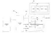
- FIG. 7illustrates a system 700 having a high-speed interface suitable for high speed TLB page transfer in accordance with an embodiment of the invention.
- the system 700can be used in a wide variety of applications, such as computer networking, data networking, instrumentation, video processing, digital processing, or any other application where the advantage of using a high speed memory device is desirable.
- the (RAMBUS DRAM) RDRAMs 702can be used to perform a variety of different memory functions, such as for example, to store executable instructions that works in cooperation with processor 102 .
- the RDRAM 702may also be used to store data used by the processor 102 in such applications as data processing, digital image manipulation programs, and the like in which fast access to a large amount of data is highly desirable.
- the system 700is only exemplary, and that the true scope and spirit of the invention should be indicated by the following claims.
- TLB page cache 114Due to performance considerations, it is desirable to have as high a transfer rate as possible into the TLB page cache 114 . Since it is well known in the art, that the inherent parallelism of DRAMs 702 - 1 through 702 - 4 supports a high transfer rate, then DRAMs 702 - 1 through 702 - 4 provide a concatenated TLB page to a TLB page cache 703 arranged as buffers 704 - 1 through 704 - 4 . However, with the advent of high speed interconnects such as those represented by RAMBUS type channels, the placement of the TLB page cache 114 can be expanded to include any location capable of being coupled to the DRAMs 702 by way of the high speed bus 708 .
- FIG. 8is a flowchart detailing a process 800 for moving a memory page temporally closer to a processor in accordance with an embodiment of the invention.
- a processorgenerates a data request having an associated virtual memory address.
- a determinationis made whether or not the requested virtual memory page has an associated TLB entry in a TLB. If it is determined that the requested memory page does not have an associated TLB entry, then the virtual memory address is translated to a physical memory address using a page table at 806 . Concurrently, at 808 , the TLB is updated with a new TLB entry corresponding to the virtual memory to physical memory translation.
- a TLB page corresponding to the new TLB entryis moved temporally closer to the processor. In one embodiment, the TLB page is moved to a local TLB page cache hierarchically located between a main memory and a cache memory.
- the requested memory pageis retrieved from the TLB page cache. In either case, the desired data element for the retrieved page is then moved to the processor for processing.
Landscapes
- Engineering & Computer Science (AREA)
- Theoretical Computer Science (AREA)
- Physics & Mathematics (AREA)
- General Engineering & Computer Science (AREA)
- General Physics & Mathematics (AREA)
- Memory System Of A Hierarchy Structure (AREA)
Abstract
Description
Claims (8)
Priority Applications (1)
| Application Number | Priority Date | Filing Date | Title |
|---|---|---|---|
| US09/491,408US6442666B1 (en) | 1999-01-28 | 2000-01-26 | Techniques for improving memory access in a virtual memory system |
Applications Claiming Priority (2)
| Application Number | Priority Date | Filing Date | Title |
|---|---|---|---|
| US11788699P | 1999-01-28 | 1999-01-28 | |
| US09/491,408US6442666B1 (en) | 1999-01-28 | 2000-01-26 | Techniques for improving memory access in a virtual memory system |
Publications (1)
| Publication Number | Publication Date |
|---|---|
| US6442666B1true US6442666B1 (en) | 2002-08-27 |
Family
ID=22375347
Family Applications (1)
| Application Number | Title | Priority Date | Filing Date |
|---|---|---|---|
| US09/491,408Expired - LifetimeUS6442666B1 (en) | 1999-01-28 | 2000-01-26 | Techniques for improving memory access in a virtual memory system |
Country Status (7)
| Country | Link |
|---|---|
| US (1) | US6442666B1 (en) |
| EP (3) | EP1157335A4 (en) |
| JP (3) | JP2002536715A (en) |
| KR (3) | KR20010101695A (en) |
| CN (3) | CN1352771A (en) |
| AU (3) | AU3352800A (en) |
| WO (3) | WO2000045267A1 (en) |
Cited By (36)
| Publication number | Priority date | Publication date | Assignee | Title |
|---|---|---|---|---|
| US20030037127A1 (en)* | 2001-02-13 | 2003-02-20 | Confluence Networks, Inc. | Silicon-based storage virtualization |
| US20030177339A1 (en)* | 2000-09-22 | 2003-09-18 | Linnermark Nils Ola | Optimization of a pipelined processor system |
| US6674441B1 (en)* | 2000-07-26 | 2004-01-06 | Ati International, Srl | Method and apparatus for improving performance of an accelerated graphics port (AGP) device |
| US20040064651A1 (en)* | 2002-09-30 | 2004-04-01 | Patrick Conway | Method and apparatus for reducing overhead in a data processing system with a cache |
| US20040148473A1 (en)* | 2003-01-27 | 2004-07-29 | Hughes William A. | Method and apparatus for injecting write data into a cache |
| US20040148380A1 (en)* | 2002-10-28 | 2004-07-29 | Richard Meyer | Method and system for dynamic expansion and contraction of nodes in a storage area network |
| US20050091458A1 (en)* | 2003-10-27 | 2005-04-28 | Yumi Sato | Storage control apparatus, control system capable of DMA transfer, and method of controlling DMA transfer |
| US7032136B1 (en) | 2001-09-07 | 2006-04-18 | Network Appliance, Inc. | Auto regression test for network-based storage virtualization system |
| US20060197221A1 (en)* | 2002-08-23 | 2006-09-07 | John Bruno | Integrated Circuit Having Memory Disposed Thereon and Method of Making Thereof |
| US20070040094A1 (en)* | 2005-04-07 | 2007-02-22 | Smith David M | Method and system for handling large data sets in a statistical language |
| US7203730B1 (en) | 2001-02-13 | 2007-04-10 | Network Appliance, Inc. | Method and apparatus for identifying storage devices |
| US20070112999A1 (en)* | 2005-11-15 | 2007-05-17 | Microsoft Corporation | Efficient power management of a system with virtual machines |
| US7334102B1 (en) | 2003-05-09 | 2008-02-19 | Advanced Micro Devices, Inc. | Apparatus and method for balanced spinlock support in NUMA systems |
| US20080133875A1 (en)* | 2006-12-05 | 2008-06-05 | Microsoft Corporation | Operational efficiency of virtual TLBs |
| US20080134174A1 (en)* | 2006-12-05 | 2008-06-05 | Microsoft Corporation | Reduction of operational costs of virtual TLBs |
| US20080155168A1 (en)* | 2006-12-22 | 2008-06-26 | Microsoft Corporation | Scalability of virtual TLBs for multi-processor virtual machines |
| US20080215848A1 (en)* | 2005-05-13 | 2008-09-04 | John Te-Jui Sheu | Method and System For Caching Address Translations From Multiple Address Spaces In Virtual Machines |
| US7472231B1 (en)* | 2001-09-07 | 2008-12-30 | Netapp, Inc. | Storage area network data cache |
| US20090106507A1 (en)* | 2007-10-22 | 2009-04-23 | Maurizio Skerlj | Memory System and Method for Using a Memory System with Virtual Address Translation Capabilities |
| US20090198955A1 (en)* | 2008-02-01 | 2009-08-06 | Arimilli Ravi K | Asynchronous memory move across physical nodes (dual-sided communication for memory move) |
| US20090198939A1 (en)* | 2008-02-01 | 2009-08-06 | Arimilli Ravi K | Launching multiple concurrent memory moves via a fully asynchronoous memory mover |
| US20090198937A1 (en)* | 2008-02-01 | 2009-08-06 | Arimilli Ravi K | Mechanisms for communicating with an asynchronous memory mover to perform amm operations |
| US20090198897A1 (en)* | 2008-02-01 | 2009-08-06 | Arimilli Ravi K | Cache management during asynchronous memory move operations |
| US20090198934A1 (en)* | 2008-02-01 | 2009-08-06 | International Business Machines Corporation | Fully asynchronous memory mover |
| US20090198936A1 (en)* | 2008-02-01 | 2009-08-06 | Arimilli Ravi K | Reporting of partially performed memory move |
| US20100161923A1 (en)* | 2008-12-19 | 2010-06-24 | Ati Technologies Ulc | Method and apparatus for reallocating memory content |
| EP2442310A2 (en)* | 2006-07-31 | 2012-04-18 | Google Inc. | Power management for memory circuit |
| WO2015002632A1 (en)* | 2013-07-01 | 2015-01-08 | Hewlett-Packard Development Company, L.P. | Lookup of a data structure containing a mapping between a virtual address space and a physical address space |
| US9311239B2 (en) | 2013-03-14 | 2016-04-12 | Intel Corporation | Power efficient level one data cache access with pre-validated tags |
| WO2016122585A1 (en)* | 2015-01-30 | 2016-08-04 | Hewlett Packard Enterprise Development Lp | Modifying characteristics of a memory segment |
| US9740613B2 (en) | 2013-09-20 | 2017-08-22 | Kabushiki Kaisha Toshiba | Cache memory system and processor system |
| US10013371B2 (en) | 2005-06-24 | 2018-07-03 | Google Llc | Configurable memory circuit system and method |
| US10515671B2 (en) | 2016-09-22 | 2019-12-24 | Advanced Micro Devices, Inc. | Method and apparatus for reducing memory access latency |
| US10847196B2 (en) | 2016-10-31 | 2020-11-24 | Rambus Inc. | Hybrid memory module |
| US11301378B2 (en) | 2017-10-12 | 2022-04-12 | Rambus Inc. | Nonvolatile physical memory with DRAM cache and mapping thereof |
| CN116055429A (en)* | 2023-01-17 | 2023-05-02 | 杭州鸿钧微电子科技有限公司 | Communication data processing method, device, device and storage medium based on PCIE |
Families Citing this family (31)
| Publication number | Priority date | Publication date | Assignee | Title |
|---|---|---|---|---|
| US6622211B2 (en)* | 2001-08-15 | 2003-09-16 | Ip-First, L.L.C. | Virtual set cache that redirects store data to correct virtual set to avoid virtual set store miss penalty |
| US6986016B2 (en)* | 2002-09-30 | 2006-01-10 | International Business Machines Corporation | Contiguous physical memory allocation |
| US7089396B2 (en)* | 2002-10-10 | 2006-08-08 | International Business Machines Corporation | Method and profiling cache for management of virtual memory |
| CN1311366C (en)* | 2003-05-22 | 2007-04-18 | 群联电子股份有限公司 | Parallel dual-rail usage method of flash memory |
| JP2005100262A (en)* | 2003-09-26 | 2005-04-14 | Seiko Epson Corp | Memory management apparatus, memory management program, and memory management method |
| US8417913B2 (en)* | 2003-11-13 | 2013-04-09 | International Business Machines Corporation | Superpage coalescing which supports read/write access to a new virtual superpage mapping during copying of physical pages |
| US7093100B2 (en)* | 2003-11-14 | 2006-08-15 | International Business Machines Corporation | Translation look aside buffer (TLB) with increased translational capacity for multi-threaded computer processes |
| US7171514B2 (en)* | 2003-11-20 | 2007-01-30 | International Business Machines Corporation | Apparatus and method to control access to logical volumes using parallel access volumes |
| US7117337B2 (en)* | 2004-02-19 | 2006-10-03 | International Business Machines Corporation | Apparatus and method for providing pre-translated segments for page translations in segmented operating systems |
| CN100414518C (en)* | 2004-11-24 | 2008-08-27 | 中国科学院计算技术研究所 | Improved virtual address transformation method and device |
| CN100414519C (en)* | 2004-11-24 | 2008-08-27 | 中国科学院计算技术研究所 | A method and device for transforming from virtual address to physical address |
| EP1717708B1 (en) | 2005-04-29 | 2010-09-01 | STMicroelectronics Srl | An improved cache memory system |
| US7609567B2 (en) | 2005-06-24 | 2009-10-27 | Metaram, Inc. | System and method for simulating an aspect of a memory circuit |
| US8111566B1 (en) | 2007-11-16 | 2012-02-07 | Google, Inc. | Optimal channel design for memory devices for providing a high-speed memory interface |
| US9171585B2 (en) | 2005-06-24 | 2015-10-27 | Google Inc. | Configurable memory circuit system and method |
| US9507739B2 (en) | 2005-06-24 | 2016-11-29 | Google Inc. | Configurable memory circuit system and method |
| US8359187B2 (en) | 2005-06-24 | 2013-01-22 | Google Inc. | Simulating a different number of memory circuit devices |
| US8397013B1 (en) | 2006-10-05 | 2013-03-12 | Google Inc. | Hybrid memory module |
| US20080082763A1 (en) | 2006-10-02 | 2008-04-03 | Metaram, Inc. | Apparatus and method for power management of memory circuits by a system or component thereof |
| US8244971B2 (en) | 2006-07-31 | 2012-08-14 | Google Inc. | Memory circuit system and method |
| US9542352B2 (en) | 2006-02-09 | 2017-01-10 | Google Inc. | System and method for reducing command scheduling constraints of memory circuits |
| US7805588B2 (en)* | 2005-10-20 | 2010-09-28 | Qualcomm Incorporated | Caching memory attribute indicators with cached memory data field |
| WO2007073624A1 (en)* | 2005-12-29 | 2007-07-05 | Intel Corporation | Virtual translation lookaside buffer |
| CN100462941C (en)* | 2006-01-26 | 2009-02-18 | 深圳艾科创新微电子有限公司 | Method for realizing memory space in configurable RISC CPU |
| EP2696290B1 (en)* | 2006-02-09 | 2015-12-23 | Google, Inc. | Memory circuit system and method |
| CN102110282A (en)* | 2011-03-14 | 2011-06-29 | 北京播思软件技术有限公司 | Screen drawing method and system for embedded equipment |
| US9058268B1 (en) | 2012-09-20 | 2015-06-16 | Matrox Graphics Inc. | Apparatus, system and method for memory management |
| CN103116556B (en)* | 2013-03-11 | 2015-05-06 | 无锡江南计算技术研究所 | Internal storage static state partition and virtualization method |
| KR101821633B1 (en) | 2013-03-14 | 2018-03-08 | 삼성전자주식회사 | Memory System |
| CN105373456B (en)* | 2015-11-19 | 2018-06-29 | 英业达科技有限公司 | Reduce the internal storage testing method of cache hit rate |
| KR102777337B1 (en)* | 2019-04-23 | 2025-03-10 | 에스케이하이닉스 주식회사 | Memory system, memory controller and operating method of thereof |
Citations (3)
| Publication number | Priority date | Publication date | Assignee | Title |
|---|---|---|---|---|
| US5630097A (en)* | 1991-06-17 | 1997-05-13 | Digital Equipment Corporation | Enhanced cache operation with remapping of pages for optimizing data relocation from addresses causing cache misses |
| US5933593A (en)* | 1997-01-22 | 1999-08-03 | Oracle Corporation | Method for writing modified data from a main memory of a computer back to a database |
| US5996055A (en) | 1997-11-26 | 1999-11-30 | Digital Equipment Corporation | Method for reclaiming physical pages of memory while maintaining an even distribution of cache page addresses within an address space |
Family Cites Families (9)
| Publication number | Priority date | Publication date | Assignee | Title |
|---|---|---|---|---|
| US4682281A (en)* | 1983-08-30 | 1987-07-21 | Amdahl Corporation | Data storage unit employing translation lookaside buffer pointer |
| DE69129252T2 (en)* | 1990-08-06 | 1998-12-17 | Ncr International, Inc., Dayton, Ohio | Method for operating a computer memory and arrangement |
| US5412787A (en)* | 1990-11-21 | 1995-05-02 | Hewlett-Packard Company | Two-level TLB having the second level TLB implemented in cache tag RAMs |
| GB9205551D0 (en)* | 1992-03-13 | 1992-04-29 | Inmos Ltd | Cache memory |
| US5574877A (en)* | 1992-09-25 | 1996-11-12 | Silicon Graphics, Inc. | TLB with two physical pages per virtual tag |
| US6356989B1 (en)* | 1992-12-21 | 2002-03-12 | Intel Corporation | Translation lookaside buffer (TLB) arrangement wherein the TLB contents retained for a task as swapped out and reloaded when a task is rescheduled |
| US5555395A (en)* | 1993-05-28 | 1996-09-10 | Dell U.S.A. L.P. | System for memory table cache reloads in a reduced number of cycles using a memory controller to set status bits in the main memory table |
| JP3135795B2 (en)* | 1994-09-22 | 2001-02-19 | 東芝マイクロエレクトロニクス株式会社 | Dynamic memory |
| US6167486A (en)* | 1996-11-18 | 2000-12-26 | Nec Electronics, Inc. | Parallel access virtual channel memory system with cacheable channels |
- 2000
- 2000-01-26USUS09/491,408patent/US6442666B1/ennot_activeExpired - Lifetime
- 2000-01-27AUAU33528/00Apatent/AU3352800A/ennot_activeAbandoned
- 2000-01-27WOPCT/US2000/002276patent/WO2000045267A1/ennot_activeApplication Discontinuation
- 2000-01-27KRKR1020017009370Apatent/KR20010101695A/ennot_activeWithdrawn
- 2000-01-27WOPCT/US2000/002401patent/WO2000045270A2/ennot_activeApplication Discontinuation
- 2000-01-27EPEP00911666Apatent/EP1157335A4/ennot_activeWithdrawn
- 2000-01-27JPJP2000596457Apatent/JP2002536715A/enactivePending
- 2000-01-27JPJP2000596461Apatent/JP2002536717A/enactivePending
- 2000-01-27AUAU36939/00Apatent/AU3693900A/ennot_activeAbandoned
- 2000-01-27AUAU36938/00Apatent/AU3693800A/ennot_activeAbandoned
- 2000-01-27JPJP2000596460Apatent/JP2002536716A/enactivePending
- 2000-01-27EPEP00915710.8Apatent/EP1196850B1/ennot_activeExpired - Lifetime
- 2000-01-27KRKR1020017009369Apatent/KR20010101694A/ennot_activeWithdrawn
- 2000-01-27CNCN00805639.0Apatent/CN1352771A/enactivePending
- 2000-01-27CNCNB008056056Apatent/CN1158607C/ennot_activeExpired - Fee Related
- 2000-01-27WOPCT/US2000/002403patent/WO2000045271A1/ennot_activeApplication Discontinuation
- 2000-01-27KRKR1020017009368Apatent/KR20010101693A/ennot_activeWithdrawn
- 2000-01-27CNCNB00805780XApatent/CN1160631C/ennot_activeExpired - Lifetime
- 2000-01-27EPEP00915711Apatent/EP1181644A4/ennot_activeWithdrawn
Patent Citations (3)
| Publication number | Priority date | Publication date | Assignee | Title |
|---|---|---|---|---|
| US5630097A (en)* | 1991-06-17 | 1997-05-13 | Digital Equipment Corporation | Enhanced cache operation with remapping of pages for optimizing data relocation from addresses causing cache misses |
| US5933593A (en)* | 1997-01-22 | 1999-08-03 | Oracle Corporation | Method for writing modified data from a main memory of a computer back to a database |
| US5996055A (en) | 1997-11-26 | 1999-11-30 | Digital Equipment Corporation | Method for reclaiming physical pages of memory while maintaining an even distribution of cache page addresses within an address space |
Non-Patent Citations (1)
| Title |
|---|
| Compaq Computer Corporation, "Alpha 21264 Microprocessor Hardware Referance Manual", Jul. 1999, pp. 2-11 & 2-12.* |
Cited By (71)
| Publication number | Priority date | Publication date | Assignee | Title |
|---|---|---|---|---|
| US6674441B1 (en)* | 2000-07-26 | 2004-01-06 | Ati International, Srl | Method and apparatus for improving performance of an accelerated graphics port (AGP) device |
| US20030177339A1 (en)* | 2000-09-22 | 2003-09-18 | Linnermark Nils Ola | Optimization of a pipelined processor system |
| US7203730B1 (en) | 2001-02-13 | 2007-04-10 | Network Appliance, Inc. | Method and apparatus for identifying storage devices |
| US7734712B1 (en) | 2001-02-13 | 2010-06-08 | Netapp, Inc. | Method and system for identifying storage devices |
| US20030037127A1 (en)* | 2001-02-13 | 2003-02-20 | Confluence Networks, Inc. | Silicon-based storage virtualization |
| US20050027754A1 (en)* | 2001-02-13 | 2005-02-03 | Candera, Inc. | System and method for policy based storage provisioning and management |
| US7594024B2 (en) | 2001-02-13 | 2009-09-22 | Netapp, Inc. | Silicon-based storage virtualization |
| US7065616B2 (en) | 2001-02-13 | 2006-06-20 | Network Appliance, Inc. | System and method for policy based storage provisioning and management |
| US8132058B1 (en) | 2001-09-07 | 2012-03-06 | Netapp, Inc. | Auto regression tester for network-based storage virtualization system |
| US9804788B2 (en) | 2001-09-07 | 2017-10-31 | Netapp, Inc. | Method and apparatus for transferring information between different streaming protocols at wire speed |
| US7032136B1 (en) | 2001-09-07 | 2006-04-18 | Network Appliance, Inc. | Auto regression test for network-based storage virtualization system |
| US7472231B1 (en)* | 2001-09-07 | 2008-12-30 | Netapp, Inc. | Storage area network data cache |
| US20060197221A1 (en)* | 2002-08-23 | 2006-09-07 | John Bruno | Integrated Circuit Having Memory Disposed Thereon and Method of Making Thereof |
| US8193635B2 (en)* | 2002-08-23 | 2012-06-05 | Ati Technologies Ulc | Integrated circuit having memory and router disposed thereon and method of making thereof |
| US20040064651A1 (en)* | 2002-09-30 | 2004-04-01 | Patrick Conway | Method and apparatus for reducing overhead in a data processing system with a cache |
| US7062610B2 (en)* | 2002-09-30 | 2006-06-13 | Advanced Micro Devices, Inc. | Method and apparatus for reducing overhead in a data processing system with a cache |
| US7752294B2 (en)* | 2002-10-28 | 2010-07-06 | Netapp, Inc. | Method and system for dynamic expansion and contraction of nodes in a storage area network |
| US20040148380A1 (en)* | 2002-10-28 | 2004-07-29 | Richard Meyer | Method and system for dynamic expansion and contraction of nodes in a storage area network |
| US7155572B2 (en) | 2003-01-27 | 2006-12-26 | Advanced Micro Devices, Inc. | Method and apparatus for injecting write data into a cache |
| US20040148473A1 (en)* | 2003-01-27 | 2004-07-29 | Hughes William A. | Method and apparatus for injecting write data into a cache |
| US7334102B1 (en) | 2003-05-09 | 2008-02-19 | Advanced Micro Devices, Inc. | Apparatus and method for balanced spinlock support in NUMA systems |
| US20050091458A1 (en)* | 2003-10-27 | 2005-04-28 | Yumi Sato | Storage control apparatus, control system capable of DMA transfer, and method of controlling DMA transfer |
| WO2006110485A3 (en)* | 2005-04-07 | 2007-03-22 | Insightful Corp | Method and system for handling large data sets in a statistical language |
| US7739311B2 (en) | 2005-04-07 | 2010-06-15 | Tibco Software Inc. | Method and system for handling large data sets in a statistical language |
| US20070040094A1 (en)* | 2005-04-07 | 2007-02-22 | Smith David M | Method and system for handling large data sets in a statistical language |
| US20080215848A1 (en)* | 2005-05-13 | 2008-09-04 | John Te-Jui Sheu | Method and System For Caching Address Translations From Multiple Address Spaces In Virtual Machines |
| US8095771B2 (en) | 2005-05-13 | 2012-01-10 | Microsoft Corporation | Method and system for caching address translations from multiple address spaces in virtual machines |
| US10013371B2 (en) | 2005-06-24 | 2018-07-03 | Google Llc | Configurable memory circuit system and method |
| US20070112999A1 (en)* | 2005-11-15 | 2007-05-17 | Microsoft Corporation | Efficient power management of a system with virtual machines |
| US8909946B2 (en) | 2005-11-15 | 2014-12-09 | Microsoft Corporation | Efficient power management of a system with virtual machines |
| US9218047B2 (en) | 2005-11-15 | 2015-12-22 | Microsoft Technology Licensing, Llc | Efficient power management of a system with virtual machines |
| US9489035B2 (en) | 2005-11-15 | 2016-11-08 | Microsoft Technology Licensing, Llc | Efficient power management of a system with virtual machines |
| US9772860B2 (en) | 2005-11-15 | 2017-09-26 | Microsoft Technology Licensing, Llc | Efficient power management of a system with virtual machines |
| EP2442310A2 (en)* | 2006-07-31 | 2012-04-18 | Google Inc. | Power management for memory circuit |
| US9104594B2 (en) | 2006-12-05 | 2015-08-11 | Microsoft Technology Licensing, Llc | Operational efficiency of virtual TLBs |
| US8615643B2 (en) | 2006-12-05 | 2013-12-24 | Microsoft Corporation | Operational efficiency of virtual TLBs |
| US20080134174A1 (en)* | 2006-12-05 | 2008-06-05 | Microsoft Corporation | Reduction of operational costs of virtual TLBs |
| US20080133875A1 (en)* | 2006-12-05 | 2008-06-05 | Microsoft Corporation | Operational efficiency of virtual TLBs |
| US8694712B2 (en) | 2006-12-05 | 2014-04-08 | Microsoft Corporation | Reduction of operational costs of virtual TLBs |
| US7788464B2 (en) | 2006-12-22 | 2010-08-31 | Microsoft Corporation | Scalability of virtual TLBs for multi-processor virtual machines |
| US20080155168A1 (en)* | 2006-12-22 | 2008-06-26 | Microsoft Corporation | Scalability of virtual TLBs for multi-processor virtual machines |
| US20090106507A1 (en)* | 2007-10-22 | 2009-04-23 | Maurizio Skerlj | Memory System and Method for Using a Memory System with Virtual Address Translation Capabilities |
| DE102008048630B4 (en)* | 2007-10-22 | 2016-04-28 | Polaris Innovations Ltd. | Storage arrangement and storage system |
| US8185716B2 (en) | 2007-10-22 | 2012-05-22 | Qimonda Ag | Memory system and method for using a memory system with virtual address translation capabilities |
| US20090198934A1 (en)* | 2008-02-01 | 2009-08-06 | International Business Machines Corporation | Fully asynchronous memory mover |
| US20090198939A1 (en)* | 2008-02-01 | 2009-08-06 | Arimilli Ravi K | Launching multiple concurrent memory moves via a fully asynchronoous memory mover |
| US8356151B2 (en) | 2008-02-01 | 2013-01-15 | International Business Machines Corporation | Reporting of partially performed memory move |
| US8275963B2 (en) | 2008-02-01 | 2012-09-25 | International Business Machines Corporation | Asynchronous memory move across physical nodes with dual-sided communication |
| US8245004B2 (en) | 2008-02-01 | 2012-08-14 | International Business Machines Corporation | Mechanisms for communicating with an asynchronous memory mover to perform AMM operations |
| US20090198937A1 (en)* | 2008-02-01 | 2009-08-06 | Arimilli Ravi K | Mechanisms for communicating with an asynchronous memory mover to perform amm operations |
| US20090198897A1 (en)* | 2008-02-01 | 2009-08-06 | Arimilli Ravi K | Cache management during asynchronous memory move operations |
| US8327101B2 (en) | 2008-02-01 | 2012-12-04 | International Business Machines Corporation | Cache management during asynchronous memory move operations |
| US20090198955A1 (en)* | 2008-02-01 | 2009-08-06 | Arimilli Ravi K | Asynchronous memory move across physical nodes (dual-sided communication for memory move) |
| US20090198936A1 (en)* | 2008-02-01 | 2009-08-06 | Arimilli Ravi K | Reporting of partially performed memory move |
| US8095758B2 (en)* | 2008-02-01 | 2012-01-10 | International Business Machines Corporation | Fully asynchronous memory mover |
| US8015380B2 (en)* | 2008-02-01 | 2011-09-06 | International Business Machines Corporation | Launching multiple concurrent memory moves via a fully asynchronoous memory mover |
| US20100161923A1 (en)* | 2008-12-19 | 2010-06-24 | Ati Technologies Ulc | Method and apparatus for reallocating memory content |
| US9569349B2 (en)* | 2008-12-19 | 2017-02-14 | Ati Technologies Ulc | Method and apparatus for reallocating memory content |
| US9311239B2 (en) | 2013-03-14 | 2016-04-12 | Intel Corporation | Power efficient level one data cache access with pre-validated tags |
| WO2015002632A1 (en)* | 2013-07-01 | 2015-01-08 | Hewlett-Packard Development Company, L.P. | Lookup of a data structure containing a mapping between a virtual address space and a physical address space |
| US9740613B2 (en) | 2013-09-20 | 2017-08-22 | Kabushiki Kaisha Toshiba | Cache memory system and processor system |
| WO2016122585A1 (en)* | 2015-01-30 | 2016-08-04 | Hewlett Packard Enterprise Development Lp | Modifying characteristics of a memory segment |
| US10515671B2 (en) | 2016-09-22 | 2019-12-24 | Advanced Micro Devices, Inc. | Method and apparatus for reducing memory access latency |
| US10847196B2 (en) | 2016-10-31 | 2020-11-24 | Rambus Inc. | Hybrid memory module |
| US11456025B2 (en) | 2016-10-31 | 2022-09-27 | Rambus Inc. | Hybrid memory module |
| US12213548B2 (en) | 2016-10-31 | 2025-02-04 | Rambus Inc. | Hybrid memory module |
| US11301378B2 (en) | 2017-10-12 | 2022-04-12 | Rambus Inc. | Nonvolatile physical memory with DRAM cache and mapping thereof |
| US11714752B2 (en) | 2017-10-12 | 2023-08-01 | Rambus Inc. | Nonvolatile physical memory with DRAM cache |
| US20230359559A1 (en)* | 2017-10-12 | 2023-11-09 | Rambus Inc. | Nonvolatile Physical Memory with DRAM Cache |
| US12135645B2 (en)* | 2017-10-12 | 2024-11-05 | Rambus Inc. | Nonvolatile physical memory with DRAM cache |
| CN116055429A (en)* | 2023-01-17 | 2023-05-02 | 杭州鸿钧微电子科技有限公司 | Communication data processing method, device, device and storage medium based on PCIE |
Also Published As
| Publication number | Publication date |
|---|---|
| AU3352800A (en) | 2000-08-18 |
| EP1157335A4 (en) | 2004-05-26 |
| EP1181644A4 (en) | 2004-05-19 |
| EP1196850A4 (en) | 2004-05-26 |
| WO2000045267A1 (en) | 2000-08-03 |
| KR20010101693A (en) | 2001-11-14 |
| CN1352771A (en) | 2002-06-05 |
| EP1196850A1 (en) | 2002-04-17 |
| JP2002536716A (en) | 2002-10-29 |
| WO2000045271A1 (en) | 2000-08-03 |
| EP1181644A1 (en) | 2002-02-27 |
| CN1158607C (en) | 2004-07-21 |
| AU3693800A (en) | 2000-08-18 |
| WO2000045270A2 (en) | 2000-08-03 |
| CN1160631C (en) | 2004-08-04 |
| KR20010101694A (en) | 2001-11-14 |
| JP2002536717A (en) | 2002-10-29 |
| EP1157335A1 (en) | 2001-11-28 |
| EP1196850B1 (en) | 2016-08-24 |
| WO2000045270A8 (en) | 2001-03-15 |
| AU3693900A (en) | 2000-08-18 |
| JP2002536715A (en) | 2002-10-29 |
| CN1347526A (en) | 2002-05-01 |
| CN1352772A (en) | 2002-06-05 |
| KR20010101695A (en) | 2001-11-14 |
| WO2000045271A9 (en) | 2001-10-04 |
Similar Documents
| Publication | Publication Date | Title |
|---|---|---|
| US6442666B1 (en) | Techniques for improving memory access in a virtual memory system | |
| WO2000045270A1 (en) | Techniques for improving memory access in a virtual memory system | |
| EP0729102B1 (en) | Cachability attributes for virtual addresses in virtually and physically indexed caches | |
| US6965970B2 (en) | List based method and apparatus for selective and rapid cache flushes | |
| US5875451A (en) | Computer hybrid memory including DRAM and EDRAM memory components, with secondary cache in EDRAM for DRAM | |
| US6782453B2 (en) | Storing data in memory | |
| US5809562A (en) | Cache array select logic allowing cache array size to differ from physical page size | |
| US20020095552A1 (en) | Highly efficient design of storage array for use in caches and memory subsystems | |
| US5809526A (en) | Data processing system and method for selective invalidation of outdated lines in a second level memory in response to a memory request initiated by a store operation | |
| US7496730B2 (en) | System and method for reducing the number of translation buffer invalidates an operating system needs to issue | |
| US6535961B2 (en) | Spatial footprint prediction | |
| US6976117B2 (en) | Snoopy virtual level 1 cache tag | |
| US6480940B1 (en) | Method of controlling cache memory in multiprocessor system and the multiprocessor system based on detection of predetermined software module | |
| US12189535B2 (en) | Tiered memory caching | |
| US12399839B1 (en) | Dynamically controlled cache rinsing |
Legal Events
| Date | Code | Title | Description |
|---|---|---|---|
| AS | Assignment | Owner name:INFINEON TECHNOLOGIES AG, GERMANY Free format text:ASSIGNMENT OF ASSIGNORS INTEREST;ASSIGNOR:STRACOVSKY, HENRY;REEL/FRAME:011048/0294 Effective date:20000810 | |
| STCF | Information on status: patent grant | Free format text:PATENTED CASE | |
| FPAY | Fee payment | Year of fee payment:4 | |
| AS | Assignment | Owner name:QIMONDA AG,GERMANY Free format text:ASSIGNMENT OF ASSIGNORS INTEREST;ASSIGNOR:INFINEON TECHNOLOGIES AG;REEL/FRAME:023768/0001 Effective date:20060425 Owner name:QIMONDA AG, GERMANY Free format text:ASSIGNMENT OF ASSIGNORS INTEREST;ASSIGNOR:INFINEON TECHNOLOGIES AG;REEL/FRAME:023768/0001 Effective date:20060425 | |
| FPAY | Fee payment | Year of fee payment:8 | |
| FPAY | Fee payment | Year of fee payment:12 | |
| AS | Assignment | Owner name:INFINEON TECHNOLOGIES AG, GERMANY Free format text:ASSIGNMENT OF ASSIGNORS INTEREST;ASSIGNOR:QIMONDA AG;REEL/FRAME:035623/0001 Effective date:20141009 | |
| AS | Assignment | Owner name:POLARIS INNOVATIONS LIMITED, IRELAND Free format text:ASSIGNMENT OF ASSIGNORS INTEREST;ASSIGNOR:INFINEON TECHNOLOGIES AG;REEL/FRAME:036575/0368 Effective date:20150708 |