US6442657B1 - Flag generation scheme for FIFOs - Google Patents
Flag generation scheme for FIFOsDownload PDFInfo
- Publication number
- US6442657B1 US6442657B1US09/371,237US37123799AUS6442657B1US 6442657 B1US6442657 B1US 6442657B1US 37123799 AUS37123799 AUS 37123799AUS 6442657 B1US6442657 B1US 6442657B1
- Authority
- US
- United States
- Prior art keywords
- flag
- address
- signal
- circuit
- response
- Prior art date
- Legal status (The legal status is an assumption and is not a legal conclusion. Google has not performed a legal analysis and makes no representation as to the accuracy of the status listed.)
- Expired - Lifetime
Links
Images


Classifications
- G—PHYSICS
- G06—COMPUTING OR CALCULATING; COUNTING
- G06F—ELECTRIC DIGITAL DATA PROCESSING
- G06F5/00—Methods or arrangements for data conversion without changing the order or content of the data handled
- G06F5/06—Methods or arrangements for data conversion without changing the order or content of the data handled for changing the speed of data flow, i.e. speed regularising or timing, e.g. delay lines, FIFO buffers; over- or underrun control therefor
- G06F5/10—Methods or arrangements for data conversion without changing the order or content of the data handled for changing the speed of data flow, i.e. speed regularising or timing, e.g. delay lines, FIFO buffers; over- or underrun control therefor having a sequence of storage locations each being individually accessible for both enqueue and dequeue operations, e.g. using random access memory
- G06F5/12—Means for monitoring the fill level; Means for resolving contention, i.e. conflicts between simultaneous enqueue and dequeue operations
- G06F5/14—Means for monitoring the fill level; Means for resolving contention, i.e. conflicts between simultaneous enqueue and dequeue operations for overflow or underflow handling, e.g. full or empty flags
- G—PHYSICS
- G06—COMPUTING OR CALCULATING; COUNTING
- G06F—ELECTRIC DIGITAL DATA PROCESSING
- G06F5/00—Methods or arrangements for data conversion without changing the order or content of the data handled
- G06F5/06—Methods or arrangements for data conversion without changing the order or content of the data handled for changing the speed of data flow, i.e. speed regularising or timing, e.g. delay lines, FIFO buffers; over- or underrun control therefor
- G06F5/10—Methods or arrangements for data conversion without changing the order or content of the data handled for changing the speed of data flow, i.e. speed regularising or timing, e.g. delay lines, FIFO buffers; over- or underrun control therefor having a sequence of storage locations each being individually accessible for both enqueue and dequeue operations, e.g. using random access memory
- G06F5/12—Means for monitoring the fill level; Means for resolving contention, i.e. conflicts between simultaneous enqueue and dequeue operations
- G—PHYSICS
- G06—COMPUTING OR CALCULATING; COUNTING
- G06F—ELECTRIC DIGITAL DATA PROCESSING
- G06F2205/00—Indexing scheme relating to group G06F5/00; Methods or arrangements for data conversion without changing the order or content of the data handled
- G06F2205/12—Indexing scheme relating to groups G06F5/12 - G06F5/14
- G06F2205/126—Monitoring of intermediate fill level, i.e. with additional means for monitoring the fill level, e.g. half full flag, almost empty flag
Definitions
- the present inventionrelates to FIFO buffers generally, and more particularly, to a method for generating FIFO status flags in a hybrid embedded Dual-Port/FIFO memory.
- Conventional flag generation circuits used in first-in first-out (FIFO) memoriescan use four dedicated flag address counters.
- Conventional depth expansion logicis implemented as part of the flag logic circuit. Consequently, changes in the depth expansion logic are made within the flag logic.
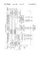
- the circuit 10comprises an array read address counter 12 , an array write address counter 14 , a memory array 16 , a flag address block 18 , and a flag logic block 20 .
- the circuit 10increases the die size due to the required separation of the array address counters 12 and 14 from the flag address circuit 18 .
- the array read address counter 12is coupled to the memory array 16 .
- An enable read signal ENRCLKis presented to the array read address counter 12 as well as to the flag address circuit 18 .
- the array write address counter 14is also coupled to the memory array 16 .
- An enable write signal ENWCLKis presented to the array write address counter 14 as well as to the flag address circuit 18 .
- the flag/array address circuit 18comprises a read address counter 22 , a read address+1 counter 24 , a write address 10 counter 26 , and a write address+1 counter 28 .
- the enable read signal ENRCLKis presented to the read address counter 22 and the read address+1 counter 24 .
- the read address counter 22presents a read signal RADDRESS in response to the enable read signal ENRCLK.
- the read address+1 counter 24presents read plus one signal RADDRESS+1 in response to the enable read signal ENRCLK.
- the enable write signal ENWCLKis presented to the write address counter 26 and the write address+1 counter 28 .
- the write address counter 26presents a write signal WADDRESS in response to the enable write signal ENWCLK.
- the write address+1 counter 28presents a write plus one signal WADDRESS+1 in response to the enable write signal ENWCLK.
- the flag logic 20presents a plurality of control signals in response to the signal RADDRESS, the signal RADDRESS+1, the signal WADDRESS, the signal WADDRESS+1, a depth control signal DEPTH CONTROL and an offset signal OFFSET.
- the flag logic circuit 20comprises an empty/full flag decoder 32 , a half full flag and depth control logic 34 , and a programmable flag and depth control logic 36 , which each receive the signal RADDRESS, the signal RADDRESS+1, the signal WADDRESS, the signal WADDRESS+1, and the signal DEPTH CONTROL.
- the programmable flag and depth control logic 36receives an additional offset signal OFFSET.
- the signal DEPTH CONTROLis used within the flag logic circuit 20 .
- the depth control logicis implemented as part of the flag logic circuit 20 . Therefore, changes to the depth expansion must be made within the flag logic circuit 20 .
- the present inventionconcerns a circuit comprising a memory, a flag/array address circuit and a flag logic circuit.
- the memorymay be configured to read and write data in response to one or more memory address signals.
- the flag/array address circuitmay be configured to present one or more flag address signals in response to (i) one or more enable signals and (ii) a control signal.
- the flag logic circuitmay be configured to present one or more logic flags in response to the one or more flag address signals.
- the objects, features and advantages of the present inventionmay include implementing a flag generation scheme that may (i) provide a highly efficient architecture for generating flag logic addresses and array addresses, (ii) save real estate in an embedded design by sharing the array address with the flag address, (iii) implement the depth control circuitry separately from the flag logic circuitry, (iv) implement a depth control circuit that may be programmed without changing the flag logic, and/or (v) provide a portable flag generation block that may easily augment a Dual-Port design for use as a FIFO.
- FIG. 1illustrates a diagram of a conventional FIFO flag generation logic circuit
- FIG. 2illustrates a block diagram illustrating a preferred embodiment of the present invention
- FIG. 3illustrates a more detailed block diagram of the circuit of FIG. 2 .
- the present inventionconcerns a circuit and method for generating FIFO logic flags.
- An address generation circuitmay be shared by a flag address generation circuit and array address generation circuit that may reduce the die size in embedded FIFO designs.
- the present inventionmay be implemented as a portable design that may allow easy augmentation of the flag logic to a memory (e.g., a Dual-Port design).
- the dual port designmay be implemented as a FIFO buffer.
- the present inventionmay also allow programming of depth reconfiguration without changing the FIFO flag logic. For example, for a 4K bit array, the flag logic 140 may be implemented to be 4K in depth, and may be used in any array configurations that are less than 4K in depth.
- the depth configurationmay be reconfigured from a 4K ⁇ 1 to a 2K ⁇ 2, 1K ⁇ 4, 1 ⁇ 2K ⁇ 8, etc. without change of the flag logic 140 .
- configurationmay be reconfigured from a 4K ⁇ 1 to a 2K ⁇ 2, 1K ⁇ 4, 1 ⁇ 2K ⁇ 8, etc. without change of the flag logic 140 .
- the circuit 100generally comprises a memory section 110 , a flag/array addresses block (or circuit) 130 , and a flag logic block (or circuit) 140 .
- the memory 110generally writes data received at an input 111 and reads data to be presented to an output 113 .
- the memory 110may read and write data in response to a first counter signal received at an input 112 and a second counter signal received at an input 114 , respectively.
- the flag/array address circuit 130may present the first counter signal at an output 132 , the second counter signal at an output 136 and a plurality of signals at outputs 134 a - 134 n .
- the signals presented at the outputs 134 a - 134 nmay be flag address signals.
- Each of the outputs 134 a - 134 nmay present a plurality of flag address signals n, where n is an integer.
- the flag/array address circuit 130may present the first and second counter signals and the plurality of the address signals in response to a first enable signal (e.g., enable write signal ENWCLK received at an input 137 ), a second enable signal (e.g., enable read signal ENRCLK received at an input 138 ), a control signal (e.g., control signal DEPTH CONTROL received at an input 138 ) and an offset signal (e.g., OFFSET received at an input 141 ).
- the signal DEPTH CONTROLmay be a multi-bit signal.
- the signal DEPTH CONTROLmay be used, in one example, to mask one or more unused address bits.
- the flag logic circuit 140generally presents a plurality of status flag signals at a number of outputs 144 a - 144 n in response to one or more of the plurality of address signals received at inputs 142 a - 142 n .
- the status flags presented at the outputs 144 a - 144 nmaybe a full flag (e.g., FF), an empty flag (e.g., EF), a half full flag (e.g., HF), a programmable almost empty flag (e.g., PAE), a programmable almost full flag (e.g., PAF), or other appropriate status flag required to meet the design criteria of a particular implementation.
- the memory 110generally comprises a first decoder 202 , a second decoder 204 and a memory array 206 .
- the first decoder 202may present a first decoded signal to an input 208 of the memory array 206 .
- the first decoded signalmay be generated in response to the first counter signal received at the input 112 .
- the second decoder 204may present a second decoded signal to an input 210 of the memory array 206 .
- the second decoded signalmay be generated in response to the second counter signal received at the input 114 .
- first counter signalmay be a read address signal (e.g., read address plus one signal RADDRESS+1) and the second counter signal may be a write address signal (e.g., write address signal WADDRESS).
- the flag/array address circuit 130generally comprises a counter 230 , a delay logic and register bank 232 , a counter 234 , and a +1 logic and register bank 236 .
- the counter 230may be implemented, in one example, as an array read address+1 counter.
- the counter 234may be implemented, in one example, as an array write address counter.
- the array read address+1 counter 230may present the read address plus one signal RADDRESS+1 at an output 231 in response to the enable read signal ENRCLK and the control signal DEPTH CONTROL.
- the enable read signal ENRCLK and the read address plus one signal RADDRESS+1may also be presented to the delay logic and register bank 232 .
- the delay logic and register bank 232may present a read address signal (e.g., read address signal RADDRESS) at an output 233 in response to the enable read signal ENRCLK and the read plus one address RADDRESS+1.
- the array write address counter 234may present a write address signal (e.g., write address signal WADDRESS) at an output 235 in response to the enable write signal ENWCLK and the control signal DEPTH CONTROL.
- the enable write signal ENWCLK, the control signal DEPTH CONTROL and the write address signal WADDRESSmay also be presented to the +1 logic and register bank 236 .
- the +1 logic and register bank 236may present a write address signal (e.g., write address plus one signal WADDRESS+1) at an output 237 in response to the enable write signal ENWCLK, the control signal DEPTH CONTROL and the write address signal WADDRESS.
- the first flag address signal of each of the plurality of flag address signals 134 a - 134 ngenerally comprises the write address plus one signal WADDRESS+1.
- the second flag address signals of each of the plurality of flag address signals 134 a - 134 ngenerally comprises the read address signal RADDRESS.
- the third flag address signal of each of the plurality of flag address signals 134 a - 134 ngenerally comprises the write address signal WADDRESS.
- the last flag address signal of each of the plurality of address signals 134 a - 134 ngenerally comprises of the read address plus one signal RADDRESS+1.
- other appropriate signalsmay be presented at the outputs 134 a - 134 n to meet the design criteria of a particular implementation.
- the flag logic circuit 140generally presents one or more status flag signals at one or more of the outputs 144 a - 144 n .
- the status flag signalsmay be generated in response to the plurality of address signals received at inputs 142 a - 142 n .
- the flag logic circuit 140generally comprises an empty/full flag decoder 252 , a half full flag decoder 254 , a programmable flag decoder 256 , a state machine 258 , a state machine 260 , a state machine 262 , a register 264 , and a register 266 .
- the empty/full flag decoder 252generally presents a first signal to the state machine 258 and a second signal to the state machine 260 in response to the plurality of address signals received at the input 142 a .
- the state machine 258may be implemented as a full flag state machine and the state machine 260 may be implemented as an empty flag state machine.
- the full flag state machine 258may present the status flag FF at the output 144 a .
- the empty flag state machine 260may present the status flag EF at the output 144 b.
- the half-full flag decoder 254generally presents a third signal to the state machine 262 in response to the plurality of address signals received at input 142 b .
- the state machine 262may be implemented as a half-full flag state machine.
- the half-full flag state machine 262may present the status flag HF at the output 144 c.
- the programmable full flag decoder 256generally presents a first output to the register 264 and a second output to the register 266 , each in response to the plurality of address signals received at the input 142 n and the signal OFFSET received at an input 268 .
- the register 264may present the status flag PAE at the output 144 d .
- the register 266may present the status flag PAF at the output 144 n.
- Examples of the empty/full flag decoder 252 , the half-full flag decoder 254 , the programmable flag decoder 256 , the full flag state machine 258 , the empty flag state machine 260 , and/or the half-full flag state machinemay be found in one or more of the following U.S. Pat. Nos. (i) 5,712,992, (ii) 5,809,339, (iii) 5,627,797, (iv) 5,850,568 and/or (v) 5,852,748, the relevant portions of each which are hereby incorporated by reference.
- the array read address+1 counter 230may be used to generate the read address plus one signal RADDRESS+1.
- the array write address counter 234may be used to generate the write address signal WADDRESS.
- the delay logic and register bank 232may be used to generate the read address signal RADDRESS.
- the +1 logic and register bank 236may be used to generate the write address plus one signal WADDRESS+1.
- the depth control logicmay be implemented in the array read address+1 counter 230 , the array write address counter 234 , and the +1 logic and register bank 236 of the flag addresses circuit 130 .
- the depth control logic within the flag/array address circuit 130may allow depth expansion that does not require changes within the flag logic circuit 140 .
Landscapes
- Engineering & Computer Science (AREA)
- Theoretical Computer Science (AREA)
- Physics & Mathematics (AREA)
- General Engineering & Computer Science (AREA)
- General Physics & Mathematics (AREA)
- Static Random-Access Memory (AREA)
Abstract
Description
Claims (22)
Priority Applications (1)
| Application Number | Priority Date | Filing Date | Title |
|---|---|---|---|
| US09/371,237US6442657B1 (en) | 1999-08-10 | 1999-08-10 | Flag generation scheme for FIFOs |
Applications Claiming Priority (1)
| Application Number | Priority Date | Filing Date | Title |
|---|---|---|---|
| US09/371,237US6442657B1 (en) | 1999-08-10 | 1999-08-10 | Flag generation scheme for FIFOs |
Publications (1)
| Publication Number | Publication Date |
|---|---|
| US6442657B1true US6442657B1 (en) | 2002-08-27 |
Family
ID=23463105
Family Applications (1)
| Application Number | Title | Priority Date | Filing Date |
|---|---|---|---|
| US09/371,237Expired - LifetimeUS6442657B1 (en) | 1999-08-10 | 1999-08-10 | Flag generation scheme for FIFOs |
Country Status (1)
| Country | Link |
|---|---|
| US (1) | US6442657B1 (en) |
Cited By (4)
| Publication number | Priority date | Publication date | Assignee | Title |
|---|---|---|---|---|
| US6584584B1 (en)* | 2000-04-10 | 2003-06-24 | Opentv, Inc. | Method and apparatus for detecting errors in a First-In-First-Out buffer |
| US20040006662A1 (en)* | 2002-07-03 | 2004-01-08 | Fu-Kuang Frank Chao | Preemptive round robin arbiter |
| US20050005082A1 (en)* | 2003-07-03 | 2005-01-06 | Mario Au | Sequential flow-control and FIFO memory devices that are depth expandable in standard mode operation |
| US20100005250A1 (en)* | 2008-07-02 | 2010-01-07 | Cradle Technologies, Inc. | Size and retry programmable multi-synchronous fifo |
Citations (6)
| Publication number | Priority date | Publication date | Assignee | Title |
|---|---|---|---|---|
| US5587953A (en) | 1994-07-06 | 1996-12-24 | Hyundai Electronics Industries Co., Inc. | First-in-first-out buffer memory |
| US5627797A (en) | 1995-12-14 | 1997-05-06 | Cypress Semiconductor Corporation | Full and empty flag generator for synchronous FIFOS |
| US5712992A (en) | 1995-12-06 | 1998-01-27 | Cypress Semiconductor Corporation | State machine design for generating empty and full flags in an asynchronous FIFO |
| US5809339A (en) | 1995-12-06 | 1998-09-15 | Cypress Semiconductor Corp. | State machine design for generating half-full and half-empty flags in an asynchronous FIFO |
| US5850568A (en) | 1995-12-22 | 1998-12-15 | Cypress Semiconductor Corporation | Circuit having plurality of carry/sum adders having read count, write count, and offset inputs to generate an output flag in response to FIFO fullness |
| US5852748A (en) | 1995-12-29 | 1998-12-22 | Cypress Semiconductor Corp. | Programmable read-write word line equality signal generation for FIFOs |
- 1999
- 1999-08-10USUS09/371,237patent/US6442657B1/ennot_activeExpired - Lifetime
Patent Citations (9)
| Publication number | Priority date | Publication date | Assignee | Title |
|---|---|---|---|---|
| US5587953A (en) | 1994-07-06 | 1996-12-24 | Hyundai Electronics Industries Co., Inc. | First-in-first-out buffer memory |
| US5712992A (en) | 1995-12-06 | 1998-01-27 | Cypress Semiconductor Corporation | State machine design for generating empty and full flags in an asynchronous FIFO |
| US5809339A (en) | 1995-12-06 | 1998-09-15 | Cypress Semiconductor Corp. | State machine design for generating half-full and half-empty flags in an asynchronous FIFO |
| US5991834A (en) | 1995-12-06 | 1999-11-23 | Cypress Semiconductor Corp. | State machine design for generating half-full and half-empty flags in an asynchronous FIFO |
| US6016403A (en) | 1995-12-06 | 2000-01-18 | Cypress Semiconductor Corp. | State machine design for generating empty and full flags in an asynchronous FIFO |
| US5627797A (en) | 1995-12-14 | 1997-05-06 | Cypress Semiconductor Corporation | Full and empty flag generator for synchronous FIFOS |
| US5850568A (en) | 1995-12-22 | 1998-12-15 | Cypress Semiconductor Corporation | Circuit having plurality of carry/sum adders having read count, write count, and offset inputs to generate an output flag in response to FIFO fullness |
| US6070203A (en) | 1995-12-22 | 2000-05-30 | Cypress Semiconductor Corp. | Circuit for generating almost full and almost empty flags in response to sum and carry outputs in asynchronous and synchronous FIFOS |
| US5852748A (en) | 1995-12-29 | 1998-12-22 | Cypress Semiconductor Corp. | Programmable read-write word line equality signal generation for FIFOs |
Non-Patent Citations (1)
| Title |
|---|
| 64K/128Kx9 Deep Sync FIFOs w/Retransmit & Depth Expansion, Cypress Preliminary CY7C4282 and CY7C4292, Cypress Semiconductor Corporation, Revised Nov. 6, 1997, pp. 1-16. |
Cited By (7)
| Publication number | Priority date | Publication date | Assignee | Title |
|---|---|---|---|---|
| US6584584B1 (en)* | 2000-04-10 | 2003-06-24 | Opentv, Inc. | Method and apparatus for detecting errors in a First-In-First-Out buffer |
| US20040006662A1 (en)* | 2002-07-03 | 2004-01-08 | Fu-Kuang Frank Chao | Preemptive round robin arbiter |
| US7099972B2 (en)* | 2002-07-03 | 2006-08-29 | Sun Microsystems, Inc. | Preemptive round robin arbiter |
| US20050005082A1 (en)* | 2003-07-03 | 2005-01-06 | Mario Au | Sequential flow-control and FIFO memory devices that are depth expandable in standard mode operation |
| US7209983B2 (en)* | 2003-07-03 | 2007-04-24 | Integrated Device Technology, Inc. | Sequential flow-control and FIFO memory devices that are depth expandable in standard mode operation |
| US20100005250A1 (en)* | 2008-07-02 | 2010-01-07 | Cradle Technologies, Inc. | Size and retry programmable multi-synchronous fifo |
| US8681526B2 (en) | 2008-07-02 | 2014-03-25 | Cradle Ip, Llc | Size and retry programmable multi-synchronous FIFO |
Similar Documents
| Publication | Publication Date | Title |
|---|---|---|
| US5587953A (en) | First-in-first-out buffer memory | |
| US7149139B1 (en) | Circuitry and methods for efficient FIFO memory | |
| CN100377072C (en) | First-in first-out memory system and method thereof | |
| KR19980018726A (en) | TWO PORT MEMORY FOR SIMULTANEOUSLY INPUTTING AND OUTPUTTING DATA | |
| US6600693B2 (en) | Method and circuit for driving quad data rate synchronous semiconductor memory device | |
| US20060020743A1 (en) | Multi-queue address generator for start and end addresses in a multi-queue first-in first-out memory system | |
| US5850568A (en) | Circuit having plurality of carry/sum adders having read count, write count, and offset inputs to generate an output flag in response to FIFO fullness | |
| US6708255B2 (en) | Variable input/output control device in synchronous semiconductor device | |
| US5764967A (en) | Multiple frequency memory array clocking scheme for reading and writing multiple width digital words | |
| US6240031B1 (en) | Memory architecture | |
| US6442657B1 (en) | Flag generation scheme for FIFOs | |
| US6400642B1 (en) | Memory architecture | |
| US6892269B2 (en) | Nonvolatile memory device with double serial/parallel communication interface | |
| US7443762B2 (en) | Synchronization circuit for a write operation on a semiconductor memory | |
| US5852748A (en) | Programmable read-write word line equality signal generation for FIFOs | |
| US7460431B1 (en) | Implementation of double data rate embedded memory in programmable devices | |
| US6901490B2 (en) | Read/modify/write registers | |
| US6804166B2 (en) | Method and apparatus for operating a semiconductor memory at double data transfer rate | |
| US6510486B1 (en) | Clocking scheme for independently reading and writing multiple width words from a memory array | |
| US20060155940A1 (en) | Multi-queue FIFO memory systems that utilize read chip select and device identification codes to control one-at-a-time bus access between selected FIFO memory chips | |
| US6499089B1 (en) | Method, architecture and circuitry for independently configuring a multiple array memory device | |
| US6489805B1 (en) | Circuits, architectures, and methods for generating a periodic signal in a memory | |
| US6442097B2 (en) | Virtual channel DRAM | |
| JP3567318B2 (en) | Semiconductor memory device and design method thereof | |
| US7729198B2 (en) | Synchronous memory circuit |
Legal Events
| Date | Code | Title | Description |
|---|---|---|---|
| AS | Assignment | Owner name:CYPRESS SEMICONDUCTOR CORPORATION, CALIFORNIA Free format text:ASSIGNMENT OF ASSIGNORS INTEREST;ASSIGNORS:FAN, JUNFEI;CRESS, DANIEL ERIC;REEL/FRAME:010163/0374 Effective date:19990809 | |
| STCF | Information on status: patent grant | Free format text:PATENTED CASE | |
| FPAY | Fee payment | Year of fee payment:4 | |
| REMI | Maintenance fee reminder mailed | ||
| FPAY | Fee payment | Year of fee payment:8 | |
| SULP | Surcharge for late payment | Year of fee payment:7 | |
| FPAY | Fee payment | Year of fee payment:12 | |
| AS | Assignment | Owner name:MORGAN STANLEY SENIOR FUNDING, INC., NEW YORK Free format text:SECURITY INTEREST;ASSIGNORS:CYPRESS SEMICONDUCTOR CORPORATION;SPANSION LLC;REEL/FRAME:035240/0429 Effective date:20150312 | |
| AS | Assignment | Owner name:CYPRESS SEMICONDUCTOR CORPORATION, CALIFORNIA Free format text:PARTIAL RELEASE OF SECURITY INTEREST IN PATENTS;ASSIGNOR:MORGAN STANLEY SENIOR FUNDING, INC., AS COLLATERAL AGENT;REEL/FRAME:039708/0001 Effective date:20160811 Owner name:SPANSION LLC, CALIFORNIA Free format text:PARTIAL RELEASE OF SECURITY INTEREST IN PATENTS;ASSIGNOR:MORGAN STANLEY SENIOR FUNDING, INC., AS COLLATERAL AGENT;REEL/FRAME:039708/0001 Effective date:20160811 | |
| AS | Assignment | Owner name:MONTEREY RESEARCH, LLC, CALIFORNIA Free format text:ASSIGNMENT OF ASSIGNORS INTEREST;ASSIGNOR:CYPRESS SEMICONDUCTOR CORPORATION;REEL/FRAME:040911/0238 Effective date:20160811 | |
| AS | Assignment | Owner name:MORGAN STANLEY SENIOR FUNDING, INC., NEW YORK Free format text:CORRECTIVE ASSIGNMENT TO CORRECT THE 8647899 PREVIOUSLY RECORDED ON REEL 035240 FRAME 0429. ASSIGNOR(S) HEREBY CONFIRMS THE SECURITY INTERST;ASSIGNORS:CYPRESS SEMICONDUCTOR CORPORATION;SPANSION LLC;REEL/FRAME:058002/0470 Effective date:20150312 |