US6441560B1 - Active matrix electroluminescent display device - Google Patents
Active matrix electroluminescent display deviceDownload PDFInfo
- Publication number
- US6441560B1 US6441560B1US09/642,257US64225700AUS6441560B1US 6441560 B1US6441560 B1US 6441560B1US 64225700 AUS64225700 AUS 64225700AUS 6441560 B1US6441560 B1US 6441560B1
- Authority
- US
- United States
- Prior art keywords
- pixel
- active matrix
- electroluminescent display
- electro
- display element
- Prior art date
- Legal status (The legal status is an assumption and is not a legal conclusion. Google has not performed a legal analysis and makes no representation as to the accuracy of the status listed.)
- Expired - Lifetime
Links
Images


Classifications
- G—PHYSICS
- G09—EDUCATION; CRYPTOGRAPHY; DISPLAY; ADVERTISING; SEALS
- G09G—ARRANGEMENTS OR CIRCUITS FOR CONTROL OF INDICATING DEVICES USING STATIC MEANS TO PRESENT VARIABLE INFORMATION
- G09G3/00—Control arrangements or circuits, of interest only in connection with visual indicators other than cathode-ray tubes
- G09G3/20—Control arrangements or circuits, of interest only in connection with visual indicators other than cathode-ray tubes for presentation of an assembly of a number of characters, e.g. a page, by composing the assembly by combination of individual elements arranged in a matrix no fixed position being assigned to or needed to be assigned to the individual characters or partial characters
- G09G3/22—Control arrangements or circuits, of interest only in connection with visual indicators other than cathode-ray tubes for presentation of an assembly of a number of characters, e.g. a page, by composing the assembly by combination of individual elements arranged in a matrix no fixed position being assigned to or needed to be assigned to the individual characters or partial characters using controlled light sources
- G09G3/30—Control arrangements or circuits, of interest only in connection with visual indicators other than cathode-ray tubes for presentation of an assembly of a number of characters, e.g. a page, by composing the assembly by combination of individual elements arranged in a matrix no fixed position being assigned to or needed to be assigned to the individual characters or partial characters using controlled light sources using electroluminescent panels
- G09G3/32—Control arrangements or circuits, of interest only in connection with visual indicators other than cathode-ray tubes for presentation of an assembly of a number of characters, e.g. a page, by composing the assembly by combination of individual elements arranged in a matrix no fixed position being assigned to or needed to be assigned to the individual characters or partial characters using controlled light sources using electroluminescent panels semiconductive, e.g. using light-emitting diodes [LED]
- G09G3/3208—Control arrangements or circuits, of interest only in connection with visual indicators other than cathode-ray tubes for presentation of an assembly of a number of characters, e.g. a page, by composing the assembly by combination of individual elements arranged in a matrix no fixed position being assigned to or needed to be assigned to the individual characters or partial characters using controlled light sources using electroluminescent panels semiconductive, e.g. using light-emitting diodes [LED] organic, e.g. using organic light-emitting diodes [OLED]
- G09G3/3225—Control arrangements or circuits, of interest only in connection with visual indicators other than cathode-ray tubes for presentation of an assembly of a number of characters, e.g. a page, by composing the assembly by combination of individual elements arranged in a matrix no fixed position being assigned to or needed to be assigned to the individual characters or partial characters using controlled light sources using electroluminescent panels semiconductive, e.g. using light-emitting diodes [LED] organic, e.g. using organic light-emitting diodes [OLED] using an active matrix
- G09G3/3233—Control arrangements or circuits, of interest only in connection with visual indicators other than cathode-ray tubes for presentation of an assembly of a number of characters, e.g. a page, by composing the assembly by combination of individual elements arranged in a matrix no fixed position being assigned to or needed to be assigned to the individual characters or partial characters using controlled light sources using electroluminescent panels semiconductive, e.g. using light-emitting diodes [LED] organic, e.g. using organic light-emitting diodes [OLED] using an active matrix with pixel circuitry controlling the current through the light-emitting element
- G—PHYSICS
- G09—EDUCATION; CRYPTOGRAPHY; DISPLAY; ADVERTISING; SEALS
- G09G—ARRANGEMENTS OR CIRCUITS FOR CONTROL OF INDICATING DEVICES USING STATIC MEANS TO PRESENT VARIABLE INFORMATION
- G09G2300/00—Aspects of the constitution of display devices
- G09G2300/08—Active matrix structure, i.e. with use of active elements, inclusive of non-linear two terminal elements, in the pixels together with light emitting or modulating elements
- G09G2300/0809—Several active elements per pixel in active matrix panels
- G09G2300/0819—Several active elements per pixel in active matrix panels used for counteracting undesired variations, e.g. feedback or autozeroing
- G—PHYSICS
- G09—EDUCATION; CRYPTOGRAPHY; DISPLAY; ADVERTISING; SEALS
- G09G—ARRANGEMENTS OR CIRCUITS FOR CONTROL OF INDICATING DEVICES USING STATIC MEANS TO PRESENT VARIABLE INFORMATION
- G09G2300/00—Aspects of the constitution of display devices
- G09G2300/08—Active matrix structure, i.e. with use of active elements, inclusive of non-linear two terminal elements, in the pixels together with light emitting or modulating elements
- G09G2300/0809—Several active elements per pixel in active matrix panels
- G09G2300/0842—Several active elements per pixel in active matrix panels forming a memory circuit, e.g. a dynamic memory with one capacitor
- G—PHYSICS
- G09—EDUCATION; CRYPTOGRAPHY; DISPLAY; ADVERTISING; SEALS
- G09G—ARRANGEMENTS OR CIRCUITS FOR CONTROL OF INDICATING DEVICES USING STATIC MEANS TO PRESENT VARIABLE INFORMATION
- G09G2300/00—Aspects of the constitution of display devices
- G09G2300/08—Active matrix structure, i.e. with use of active elements, inclusive of non-linear two terminal elements, in the pixels together with light emitting or modulating elements
- G09G2300/088—Active matrix structure, i.e. with use of active elements, inclusive of non-linear two terminal elements, in the pixels together with light emitting or modulating elements using a non-linear two-terminal element
- G—PHYSICS
- G09—EDUCATION; CRYPTOGRAPHY; DISPLAY; ADVERTISING; SEALS
- G09G—ARRANGEMENTS OR CIRCUITS FOR CONTROL OF INDICATING DEVICES USING STATIC MEANS TO PRESENT VARIABLE INFORMATION
- G09G2320/00—Control of display operating conditions
- G09G2320/04—Maintaining the quality of display appearance
- G09G2320/043—Preventing or counteracting the effects of ageing
- G09G2320/045—Compensation of drifts in the characteristics of light emitting or modulating elements
- G—PHYSICS
- G09—EDUCATION; CRYPTOGRAPHY; DISPLAY; ADVERTISING; SEALS
- G09G—ARRANGEMENTS OR CIRCUITS FOR CONTROL OF INDICATING DEVICES USING STATIC MEANS TO PRESENT VARIABLE INFORMATION
- G09G2360/00—Aspects of the architecture of display systems
- G09G2360/14—Detecting light within display terminals, e.g. using a single or a plurality of photosensors
- G09G2360/145—Detecting light within display terminals, e.g. using a single or a plurality of photosensors the light originating from the display screen
- G09G2360/147—Detecting light within display terminals, e.g. using a single or a plurality of photosensors the light originating from the display screen the originated light output being determined for each pixel
- G09G2360/148—Detecting light within display terminals, e.g. using a single or a plurality of photosensors the light originating from the display screen the originated light output being determined for each pixel the light being detected by light detection means within each pixel
- G—PHYSICS
- G09—EDUCATION; CRYPTOGRAPHY; DISPLAY; ADVERTISING; SEALS
- G09G—ARRANGEMENTS OR CIRCUITS FOR CONTROL OF INDICATING DEVICES USING STATIC MEANS TO PRESENT VARIABLE INFORMATION
- G09G3/00—Control arrangements or circuits, of interest only in connection with visual indicators other than cathode-ray tubes
- G09G3/20—Control arrangements or circuits, of interest only in connection with visual indicators other than cathode-ray tubes for presentation of an assembly of a number of characters, e.g. a page, by composing the assembly by combination of individual elements arranged in a matrix no fixed position being assigned to or needed to be assigned to the individual characters or partial characters
- G09G3/22—Control arrangements or circuits, of interest only in connection with visual indicators other than cathode-ray tubes for presentation of an assembly of a number of characters, e.g. a page, by composing the assembly by combination of individual elements arranged in a matrix no fixed position being assigned to or needed to be assigned to the individual characters or partial characters using controlled light sources
- G09G3/30—Control arrangements or circuits, of interest only in connection with visual indicators other than cathode-ray tubes for presentation of an assembly of a number of characters, e.g. a page, by composing the assembly by combination of individual elements arranged in a matrix no fixed position being assigned to or needed to be assigned to the individual characters or partial characters using controlled light sources using electroluminescent panels
- G09G3/32—Control arrangements or circuits, of interest only in connection with visual indicators other than cathode-ray tubes for presentation of an assembly of a number of characters, e.g. a page, by composing the assembly by combination of individual elements arranged in a matrix no fixed position being assigned to or needed to be assigned to the individual characters or partial characters using controlled light sources using electroluminescent panels semiconductive, e.g. using light-emitting diodes [LED]
- H—ELECTRICITY
- H10—SEMICONDUCTOR DEVICES; ELECTRIC SOLID-STATE DEVICES NOT OTHERWISE PROVIDED FOR
- H10K—ORGANIC ELECTRIC SOLID-STATE DEVICES
- H10K59/00—Integrated devices, or assemblies of multiple devices, comprising at least one organic light-emitting element covered by group H10K50/00
- H10K59/10—OLED displays
- H10K59/12—Active-matrix OLED [AMOLED] displays
- H10K59/13—Active-matrix OLED [AMOLED] displays comprising photosensors that control luminance
Definitions
- This inventionrelates to active matrix electroluminescent display devices comprising an array of electroluminescent display pixels. More particularly, the invention concerns an active matrix electroluminescent display device comprising an array of display pixels with each pixel comprising an electroluminescent display element and a driving device for controlling the current through the display element based on a drive signal applied to the pixel during an address period and stored as a voltage on a storage capacitance connected to the pixel driving device.
- Matrix display devicesemploying electroluminescent, light-emitting, display elements are well known.
- the display elementsmay comprise organic thin film electroluminescent elements, for example using polymer materials, or else light emitting diodes (LEDs) using traditional III-V semiconductor compounds.
- organic electroluminescent materialsparticularly polymer materials, have demonstrated their ability to be used practically for video display devices.
- These materialstypically comprise one or more layers of an electroluminescent material, for example a semiconducting conjugated polymer, sandwiched between a pair of electrodes, one of which is transparent and the other of which is of a material suitable for injecting holes or electrons into the polymer layer.
- the polymer materialcan be fabricated using a CVD process, or simply by printing or a spin coating technique using a solution of a soluble conjugated polymer.
- Organic electroluminescent materialsexhibit diode-like I-V properties, so that they are capable of providing both a display function and a switching function, and can therefore be used in passive type displays.
- the inventionis concerned with active matrix display devices, with each pixel comprising a display element and a switching device for controlling the current through the display elements.
- active matrix electroluminescent displayexamples of an active matrix electroluminescent display are described in EP-A-0653741 and EP-A-0717446.
- the electroluminescent display elementsneed to continuously pass current to generate light.
- a driving device of a pixelusually comprising a TFT (thin film transistor), is responsible for controlling the current through the display element.
- the brightness of the display elementis proportional to the current flowing through it.
- a drive (data) signalin the form of a voltage or current signal determining the required output from the display element is applied to the pixel and stored as a corresponding voltage level on a storage capacitance which is connected to, and controls the operation of, the current controlling drive device with the voltage stored on the capacitance serving to maintain operation of the switching device in supplying current through the display element during the period, corresponding to a field period, until the pixel is addressed again.
- an active matrix electroluminescent display devicecomprising an array of display pixels each comprising an electroluminescent display element and a driving device for controlling the current through the display element based on a drive signal applied to the pixel during an address period and stored as a voltage on a storage capacitance connected to the driving device, which is characterized in that each pixel includes electro-optic adjustment means which is responsive to light produced by the display element during addressing and arranged to adjust in the address period the voltage signal stored on the capacitance in accordance with the light output level of the display element.
- the stored signal voltage for determining the light output level of the display element in the drive (display) period following addressingis adjusted according to the light output characteristic of the display element, providing a feedback variable, whereby the drive level set on the pixel can compensate for the effects of ageing of the display elements so that a desired light output level from a display element for a given applied drive signal is substantially maintained regardless of possible variations in the drive current level/light output level characteristics of individual display elements in the array.
- the inventionoffers a further important advantage.
- the drive current for a display elementis determined by the voltage applied to the gate of the TFT, corresponding to the voltage stored in the capacitance. This drive current therefore depends strongly on the characteristics of the TFT and variations in the threshold voltage, mobility and dimensions of the individual TFTs of pixels of the array, for example, due to manufacturing processes, can produce unwanted variations in the display element currents and hence in the light levels produced, leading to non-uniformity in the display output.
- the effect of the electro-optic adjustment means in controlling the stored voltage signalwill also compensate for such variations in TFT characteristics.
- the inventionis particularly beneficial in devices using polymer LED materials, it can of course be applied to advantage in any electroluminescent device in which the electroluminescent material similarly suffers ageing effects resulting in lower light output levels for a given drive current over a period of time of operation.
- the electro-optic meansregulates a current flowing in the pixel during the address period according to an applied data signal upon which current the voltage stored on the capacitance following the address period is dependent.
- the electro-optic meanscomprises a photoelectric device connected to the storage capacitance via a switch device, for example, another TFT, which is arranged to be closed during the address period so as to connect the photoelectric device in parallel with the storage capacitance during the address period.
- a switch devicefor example, another TFT
- the photoelectric deviceis effectively disconnected from the storage capacitance and plays no part in the operation of the pixel.
- the photoelectric deviceserves to shunt current from the capacitance in dependence upon the display element's light output until an equilibrium state is reached and the capacitance voltage, and thus the gate voltage of the drive TFT, stabilizes.
- the photoelectric devicepreferably comprises a photodiode, although a photoresistor or phototransistor could alternatively be employed.
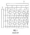
- FIG. 1is a simplified schematic diagram of a known active matrix electroluminescent display device comprising an array of pixels;
- FIG. 2shows the equivalent circuit of a few typical pixels of the known active matrix electoluminescent display device of FIG. 1;
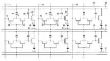
- FIG. 3shows the equivalent circuit of a few typical pixels in an embodiment of an active matrix electroluminescent display device according to the invention.
- the active matrix electroluminescent display devicecomprises a panel having a row and column matrix array of regularly-spaced pixels, denoted by the blocks 10 , each comprising an electroluminescent display element and an associated driving device controlling the current through the display element, and which are located at the intersections between crossing sets of row (selection) and column (data) address conductors, or lines, 12 and 14 . Only a few pixels are shown here for simplicity.
- the pixels 10are addressed via the sets of address conductors by a peripheral drive circuit comprising a row, scanning, driver circuit 16 and a column, data, driver circuit 18 connected to the ends of the respective sets.
- Each row of pixelsis addressed in turn by means of a selection signal applied by the circuit 16 to the relevant row conductor 12 so as to load the pixels of the row with respective drive signals, determining their individual display outputs, according to the respective data signals supplied in parallel by the circuit 18 to the column conductors.
- the appropriate data signalsare supplied by the circuit 18 in appropriate synchronisation.
- FIG. 2illustrates the circuit of a few, typical, pixels in this known device.
- the data signalscomprise voltage signals.
- Each pixel, 10includes a light emitting organic electroluminescent display element 20 , represented here as a diode element (LED), and comprising a pair of electrodes between which one or more active layers of organic electroluminescent material is sandwiched.
- the materialcomprises a polymer LED material, although other organic electroluminescent materials, such as low molecular weight materials, could be used.
- the display elements of the arrayare carried together with the associated active matrix circuitry on one side of an insulating support. Either the cathodes or the anodes of the display elements are formed of transparent conductive material.
- the supportis of transparent material such as glass and the electrodes of the individual display elements 20 closest to the substrate can consist of a transparent conductive material such as ITO so that light generated by the electroluminescent layer is transmitted through these electrodes and the support so as to be visible to a viewer at the other side of the support.
- the light outputcould be viewed from above the panel and the display element anodes in this case would comprise parts of a continuous ITO layer constituting a supply line common to all display elements in the array.
- the cathodes of the display elementscomprise a metal having a low work-function such as calcium or magnesium silver alloy. Examples of suitable organic conjugated polymer materials which can be used are described in WO 96/36959. Examples of other, low molecular weight, organic materials are described in EP-A-0717446, which also describes examples of the construction and operation of an active matrix electroluminescent device and whose disclosure in these respects is incorporated herein by reference.
- Each pixel 10includes a drive device in the form of a TFT 22 which controls the operation of the display element 20 based on an analogue data signal voltage applied to the pixel.
- the signal voltage for a pixelis supplied via a column conductor 14 which is shared between a respective column of pixels.
- the column conductor 14is coupled to the gate of the current-controlling drive transistor 22 through an address TFT 26 .
- the gates for the address TFTs 26 of a row of pixelsare coupled together to a common row conductor 12 .
- Each row of pixels 10also shares a common voltage supply line 30 , usually provided as a continuous electrode common to all pixels, and a respective common current line 32 .
- the display element 20 and the drive device 22are connected in series between the voltage supply line 30 and the common current line 32 , which is at a positive potential with respect to the supply line 30 and acts as a current source for the current flowing through the display element 20 .
- the current flowing through the display element 20is controlled by the switching device 22 and is a function of the gate voltage on the transistor 22 , which is dependent upon a stored control signal determined by the data signal supplied to the column conductor 14 .
- a row of pixelsis selected by the row driver circuit 16 applying a selection pulse to the row conductor 12 which switches on the address TFTs 26 for the respective row of pixels.
- a voltage level derived from the video informationis applied to the column conductor 14 by the driver circuit 18 and is transferred by the address TFT 26 to the gate of the drive transistor 22 .
- the address transistor 26is turned off, but the voltage on the gate of the drive transistor 22 is maintained by a pixel storage capacitor 36 which is connected between the gate of the drive transistor 22 and the common current line 32 .
- the voltage between the gate of the drive transistor 22 and the common current line 32determines the current passing through the display element 20 of the pixel 10 .
- the current flowing through the display elementis a function of the gate-source voltage of the drive transistor 22 (the source of the transistor 22 being connected to the common current line 32 , and the drain of the transistor 22 being connected to the display element 20 ). This current in turn controls the light output level (grey-scale) of the pixel.
- the switching transistor 22is arranged to operate in saturation, so that the gate-source voltage governs the current flowing through the transistor, irrespective of the drain-source voltage. Consequently, slight variations of the drain voltage do not affect the current flowing through the display element 20 .
- the voltage on the voltage supply line 30is therefore not critical to the correct operation of the pixels.
- Each row of pixelsis addressed in turn in this manner in respective row address periods so as to load the pixels of each row in sequence with their drive signals and set the pixels to provide desired display outputs for the drive (field) period until they are next addressed.
- the voltage stored on the capacitor 36is substantially determined by the applied data signal voltage and that as this voltage in turn controls the drive transistor 22 and the current through the display element 20 , then the resulting light output level of the display element at any time will be dependent on the then existing current/light output level characteristic of the display element.
- the electroluminescent material of the display elementcan suffer degradation over a period of time of operation leading to ageing effects which result in a reduction of the light output level for a given drive current level. Those pixels which have, therefore, been driven longer (or harder) will exhibit a reduced brightness and cause display non-uniformities. With polymer LED materials the effects of such ageing can be significant.
- the drive signal stored in a pixel during the addressing phaseis automatically adjusted through electro-optical means in the pixel, acting as a feedback arrangement, according to the light emission characteristic of the display element so as to compensate at least to some extent for such ageing effects and ensure that the required light output level of the display element is produced following addressing.
- the pixelfurther includes an additional switch device 40 , again in the form of a TFT, which is connected between the address TFT 26 and the node between the storage capacitor 36 and the gate of the drive transistor 22 with its gate terminal connected to the same row conductor 12 as the gate of the address TFT 26 so as to be operated simultaneously with that TFT by the application of a (gating) pulse selection signal applied to the row conductor 12 .
- an additional switch device 40again in the form of a TFT, which is connected between the address TFT 26 and the node between the storage capacitor 36 and the gate of the drive transistor 22 with its gate terminal connected to the same row conductor 12 as the gate of the address TFT 26 so as to be operated simultaneously with that TFT by the application of a (gating) pulse selection signal applied to the row conductor 12 .
- a photodiode 45is connected between the current line 32 associated with the pixel and the node between the TFTs 26 and 40 .
- the pixelis constructed in such a way that the photodiode 45 is exposed to light emitted by the display element 20 of the pixel. The purpose of such optical coupling between these components will become apparent from the following description of the operation of this pixel.
- the data signals applied to the pixels via the column conductors 14comprise analogue current signals rather than voltage signals.
- Active matrix electroluminescent devices using current rather than voltage data signalsare known, an example of such being described in W 0 99/65012 (PHB 34253).
- this pixel circuithas two states, an addressing state in which the pixel is set to the desired display output condition and a driving state in which the display element is thereafter driven according to the set condition until the pixel is again addressed in the subsequent field.
- the row driver circuit 16applies a selection pulse signal to the row conductor 12 in a respective row address period which turns on the TFTs 26 and 40 .
- the capacitor 36is assumed here for example to be fully discharged at this time.
- a currentis sunk in the associated column conductor 14 according to the applied data signal. The charge path is from the current line 32 through the storage capacitor 36 and the photodiode 45 in parallel.
- the extent of photocurrentis proportional to the light level (quantity of photons/second) received thereby even though it is reverse biased.
- the photodiode 45then shunts current from the capacitor 36 . After a short time, still within the row address period, an equilibrium state is achieved in which the current being sunk by the column conductor 14 is all shunted by the photodiode alone and the gate voltage of the drive TFT 22 stabilises.
- the light from the display element 20is used as a feedback variable, via the photodiode 45 , in the setting of the pixel during addressing.
- the pixel circuitis then switched to its drive state by the turning off of the TFTs 26 and 40 , upon termination of the row selection pulse, to isolate electrically the node between the gate of the TFT 22 and the storage capacitor 36 from the photodiode 45 and column conductor 14 .
- the capacitor 36now acts to store the gate-source voltage of the TFT 22 as an adjusted drive signal level determining the current drive level of the display element in the drive (display) phase until the pixel is next addressed. This results in a steady current flowing through the display element 20 throughout this drive period.
- the light output (photons) per second during the drive phaseis fixed according to a desired output light level, and is proportional to the input current.
- the setting of the pixelis made dependent on the instantaneous light output generating characteristic of the associated display element and the drive signal voltage stored on the capacitor 36 , and the consequential level of current through the display element determined by the TFT 22 , is automatically adjusted accordingly so as to compensate for the effects of ageing in the display element. If the light output level for a given drive current in a display element is reduced due to ageing, then the adjusted stored drive signal will cause the display element to be driven at a appropriately higher current level to maintain the desired display effect.
- the photocurrent in the photodiode 45will discharge the capacitor 36 until there is no light output from the display element 20 during this phase, and no light would be emitted in the driving phase.
- the TFTs used in the above embodiment of pixel circuitall comprise p-channel MOS TFTs.
- n-channel MOS TFTScould be used instead, with the polarity of the display element 20 and photodiode 45 , and the applied drive voltages being reversed.
- polysilicon TFTsare used, although alternatively amorphous silicon TFTs could be employed.
- the photodiode 45may be replaced by a phototransistor (diode-connected) or possibly a photoresistor or other suitable photo-electric device.
- the photodiode 45is arranged so that it is exposed to light emitted by the display element 20 , it is preferably shielded from ambient light falling on the device so that it is responsive in operation solely to light from the display element.
- an active matrix electroluminescent display devicewhich comprises an array of display pixels which each include a current-driven electroluminescent display element connected to a driving device controlling the current flowing through the display element in a drive period according to a voltage stored on a capacitance and determined by a data signal applied in a preceding address period.
- electro-optic meansare included in the pixel for adjusting the voltage stored on the capacitance in dependence on the light output of its display element during the address period.
Landscapes
- Engineering & Computer Science (AREA)
- Physics & Mathematics (AREA)
- Computer Hardware Design (AREA)
- General Physics & Mathematics (AREA)
- Theoretical Computer Science (AREA)
- Control Of Indicators Other Than Cathode Ray Tubes (AREA)
- Devices For Indicating Variable Information By Combining Individual Elements (AREA)
Abstract
Description
Claims (20)
Applications Claiming Priority (2)
| Application Number | Priority Date | Filing Date | Title |
|---|---|---|---|
| GBGB9919536.4AGB9919536D0 (en) | 1999-08-19 | 1999-08-19 | Active matrix electroluminescent display device |
| GB9919536 | 1999-08-19 |
Publications (1)
| Publication Number | Publication Date |
|---|---|
| US6441560B1true US6441560B1 (en) | 2002-08-27 |
Family
ID=10859372
Family Applications (1)
| Application Number | Title | Priority Date | Filing Date |
|---|---|---|---|
| US09/642,257Expired - LifetimeUS6441560B1 (en) | 1999-08-19 | 2000-08-18 | Active matrix electroluminescent display device |
Country Status (6)
| Country | Link |
|---|---|
| US (1) | US6441560B1 (en) |
| EP (1) | EP1135804B1 (en) |
| JP (1) | JP4393740B2 (en) |
| KR (1) | KR100712563B1 (en) |
| GB (1) | GB9919536D0 (en) |
| WO (1) | WO2001015232A1 (en) |
Cited By (40)
| Publication number | Priority date | Publication date | Assignee | Title |
|---|---|---|---|---|
| US20010055008A1 (en)* | 2000-06-20 | 2001-12-27 | U.S. Philips Corporation | Matrix array display devices with light sensing elements and associated storage capacitors |
| US20020171611A1 (en)* | 2001-05-15 | 2002-11-21 | Eastman Kodak Company | Active matrix organic light emitting diode flat-panel display |
| US20030076295A1 (en)* | 2001-10-22 | 2003-04-24 | Mutsumi Nakajima | Input device and input and output device |
| US20040119401A1 (en)* | 2002-09-30 | 2004-06-24 | Jiun-Haw Lee | [organic electroluminescent device having solar cells and fabricating method therefor] |
| US6777886B1 (en)* | 2003-04-08 | 2004-08-17 | Windell Corporation | Digital driving method and apparatus for active matrix OLED |
| WO2004088627A1 (en)* | 2003-04-04 | 2004-10-14 | Koninklijke Philips Electronics N.V. | Electroluminescent display devices |
| US20040257354A1 (en)* | 2003-06-18 | 2004-12-23 | Nuelight Corporation | Controlled passive display, apparatus and method for controlling and making a passive display |
| US20050029591A1 (en)* | 2002-12-03 | 2005-02-10 | Seiko Epson Corporation | Transistor, integrated circuit, electro-optic device, electronic instrument and method of manufacturing a transistor |
| US20050104821A1 (en)* | 2003-11-14 | 2005-05-19 | Nokia Corporation | Display arrangement |
| US20050121600A1 (en)* | 2003-12-08 | 2005-06-09 | Ting-Wei Chuang | [organic electroluminescent device and fabricating method therefor] |
| US20050128193A1 (en)* | 2003-04-07 | 2005-06-16 | Lueder Ernst H. | Methods and apparatus for a display |
| US6924602B2 (en)* | 2001-02-15 | 2005-08-02 | Sanyo Electric Co., Ltd. | Organic EL pixel circuit |
| US20050200294A1 (en)* | 2004-02-24 | 2005-09-15 | Naugler W. E.Jr. | Sidelight illuminated flat panel display and touch panel input device |
| US20050200296A1 (en)* | 2004-02-24 | 2005-09-15 | Naugler W. E.Jr. | Method and device for flat panel emissive display using shielded or partially shielded sensors to detect user screen inputs |
| US20050200293A1 (en)* | 2004-02-24 | 2005-09-15 | Naugler W. E.Jr. | Penlight and touch screen data input system and method for flat panel displays |
| US20050200292A1 (en)* | 2004-02-24 | 2005-09-15 | Naugler W. E.Jr. | Emissive display device having sensing for luminance stabilization and user light or touch screen input |
| US20050225519A1 (en)* | 2004-04-12 | 2005-10-13 | The Board Of Trustees Of The Leland Stanford Junior University | Low power circuits for active matrix emissive displays and methods of operating the same |
| US20050231580A1 (en)* | 2004-02-10 | 2005-10-20 | Seiko Epson Corporation | Line head and image forming apparatus incorporating the same |
| US20050243023A1 (en)* | 2004-04-06 | 2005-11-03 | Damoder Reddy | Color filter integrated with sensor array for flat panel display |
| US20050248515A1 (en)* | 2004-04-28 | 2005-11-10 | Naugler W E Jr | Stabilized active matrix emissive display |
| US20060022204A1 (en)* | 2002-10-08 | 2006-02-02 | Koninklijke Philips Electroics N.V. | Electroluminescent display devices |
| US20060028409A1 (en)* | 2004-08-05 | 2006-02-09 | Takaji Numao | Display device and driving method thereof |
| US20060063028A1 (en)* | 2003-04-08 | 2006-03-23 | Leurs Jeroom Frans M | Two sided light emitting device |
| US20060132451A1 (en)* | 2003-02-13 | 2006-06-22 | Koninklijke Philips Electronics N.V. | Optically addressable matrix display |
| US20060208979A1 (en)* | 2003-03-12 | 2006-09-21 | Fish David A | Light emissive active matrix display devices with optical feedback effective on the timing, to counteract ageing |
| US20060264143A1 (en)* | 2003-12-08 | 2006-11-23 | Ritdisplay Corporation | Fabricating method of an organic electroluminescent device having solar cells |
| US20070046593A1 (en)* | 2005-08-26 | 2007-03-01 | Dong-Yong Shin | Organic light emitting diode display device and driving method thereof |
| US20070103411A1 (en)* | 2005-11-07 | 2007-05-10 | Eastman Kodak Company | OLED display with aging compensation |
| US20070182674A1 (en)* | 2004-03-16 | 2007-08-09 | Koninklijke Philips Electronics, N.V. | Active matrix display devices |
| WO2005114637A3 (en)* | 2004-05-12 | 2007-08-30 | E Ink Corp | Tiled displays |
| EP1837912A1 (en)* | 2006-03-22 | 2007-09-26 | Toppoly Optoelectronics Corp. | Organic electroluminescent device and fabrication methods thereof |
| US20070236430A1 (en)* | 2004-06-05 | 2007-10-11 | Koninklijke Philips Electronics, N.V. | Active Matrix Display Devices |
| US20080111799A1 (en)* | 2004-05-25 | 2008-05-15 | Koninklijke Philips Electronics, N.V. | Driving an electroluminescent display |
| US20080203930A1 (en)* | 2005-05-19 | 2008-08-28 | Koninklijke Philips Electronics, N.V. | Electroluminescent Display Devices |
| US20090029739A1 (en)* | 2000-08-23 | 2009-01-29 | Semiconductor Energy Laboratory Co., Ltd. | Portable Electronic Device |
| WO2006076657A3 (en)* | 2005-01-12 | 2009-07-16 | Nuelight Corp | Method and apparatus for taking a reading of a sensor coupled to a light emitting element of a flat panel display |
| US20090212690A1 (en)* | 2007-12-18 | 2009-08-27 | Lumimove, Inc., D/B/A Crosslink | Flexible electroluminescent devices and systems |
| US20140028738A1 (en)* | 2003-09-23 | 2014-01-30 | Ignis Innovation Inc. | Circuit and method for driving an array of light emitting pixels |
| US20140340377A1 (en)* | 2011-11-02 | 2014-11-20 | Sharp Kabushiki Kaisha | Color display device |
| US20170069266A1 (en)* | 2006-08-15 | 2017-03-09 | Ignis Innovation Inc. | Oled luminance degradation compensation |
Families Citing this family (14)
| Publication number | Priority date | Publication date | Assignee | Title |
|---|---|---|---|---|
| JP2002278504A (en)* | 2001-03-19 | 2002-09-27 | Mitsubishi Electric Corp | Self-luminous display |
| US6812651B2 (en)* | 2001-03-22 | 2004-11-02 | Mitsubishi Denki Kabushiki Kaisha | Spontaneous light emitting display device |
| GB0113331D0 (en)* | 2001-06-01 | 2001-07-25 | Printable Field Emitters Ltd | Drive electronics for display devices |
| JP2003084733A (en)* | 2001-07-04 | 2003-03-19 | Sharp Corp | Display devices and mobile devices |
| SG148032A1 (en)* | 2001-07-16 | 2008-12-31 | Semiconductor Energy Lab | Light emitting device |
| KR100767377B1 (en)* | 2001-09-28 | 2007-10-17 | 삼성전자주식회사 | Organic EL display panel and organic EL display device having same |
| GB2381643A (en)* | 2001-10-31 | 2003-05-07 | Cambridge Display Tech Ltd | Display drivers |
| GB2381644A (en)* | 2001-10-31 | 2003-05-07 | Cambridge Display Tech Ltd | Display drivers |
| KR100940342B1 (en)* | 2001-11-13 | 2010-02-04 | 가부시키가이샤 한도오따이 에네루기 켄큐쇼 | Display device and driving method |
| US6720942B2 (en) | 2002-02-12 | 2004-04-13 | Eastman Kodak Company | Flat-panel light emitting pixel with luminance feedback |
| JP3829778B2 (en) | 2002-08-07 | 2006-10-04 | セイコーエプソン株式会社 | Electronic circuit, electro-optical device, and electronic apparatus |
| US7385572B2 (en) | 2002-09-09 | 2008-06-10 | E.I Du Pont De Nemours And Company | Organic electronic device having improved homogeneity |
| JP2004348044A (en)* | 2003-05-26 | 2004-12-09 | Seiko Epson Corp | Display device, display method, and method of manufacturing display device |
| US20250081607A1 (en)* | 2020-11-10 | 2025-03-06 | Lg Electronics Inc. | Display device using semiconductor light-emitting element |
Citations (9)
| Publication number | Priority date | Publication date | Assignee | Title |
|---|---|---|---|---|
| US4975691A (en)* | 1987-06-16 | 1990-12-04 | Interstate Electronics Corporation | Scan inversion symmetric drive |
| EP0653741A1 (en) | 1993-10-12 | 1995-05-17 | Nec Corporation | Current-controlled luminous element array and method for producing the same |
| EP0717446A2 (en) | 1994-12-14 | 1996-06-19 | Eastman Kodak Company | TFT-EL display panel using organic electroluminiscent media |
| WO1996036959A2 (en) | 1995-05-19 | 1996-11-21 | Philips Electronics N.V. | Display device |
| EP0923067A1 (en) | 1997-03-12 | 1999-06-16 | Seiko Epson Corporation | Pixel circuit, display device and electronic equipment having current-driven light-emitting device |
| US5973456A (en)* | 1996-01-30 | 1999-10-26 | Denso Corporation | Electroluminescent display device having uniform display element column luminosity |
| WO1999065012A2 (en) | 1998-06-12 | 1999-12-16 | Koninklijke Philips Electronics N.V. | Active matrix electroluminescent display devices |
| US6057647A (en)* | 1998-02-24 | 2000-05-02 | Casio Computer Co., Ltd. | Light emitting device used for display device |
| US6191764B1 (en)* | 1997-04-14 | 2001-02-20 | Casio Computer Co., Ltd. | Method of driving display device |
Family Cites Families (5)
| Publication number | Priority date | Publication date | Assignee | Title |
|---|---|---|---|---|
| JPH0723987B2 (en)* | 1984-02-24 | 1995-03-15 | 財団法人日本交通管理技術協会 | Information display device |
| JP2577034B2 (en)* | 1988-03-18 | 1997-01-29 | 日本板硝子株式会社 | Self-scanning light emitting element array and driving method thereof |
| EP0845812B1 (en)* | 1996-11-28 | 2009-10-28 | Casio Computer Co., Ltd. | Display apparatus |
| JPH10319896A (en)* | 1997-05-15 | 1998-12-04 | Sony Corp | Information display device and method of detecting and adjusting display condition and controlling maintenance method |
| EP0974140A2 (en)* | 1998-02-06 | 2000-01-26 | Koninklijke Philips Electronics N.V. | Organic electroluminescent device |
- 1999
- 1999-08-19GBGBGB9919536.4Apatent/GB9919536D0/ennot_activeCeased
- 2000
- 2000-08-02KRKR1020017004825Apatent/KR100712563B1/ennot_activeExpired - Lifetime
- 2000-08-02JPJP2001519495Apatent/JP4393740B2/ennot_activeExpired - Lifetime
- 2000-08-02EPEP00960385.3Apatent/EP1135804B1/ennot_activeExpired - Lifetime
- 2000-08-02WOPCT/EP2000/007520patent/WO2001015232A1/enactiveIP Right Grant
- 2000-08-18USUS09/642,257patent/US6441560B1/ennot_activeExpired - Lifetime
Patent Citations (9)
| Publication number | Priority date | Publication date | Assignee | Title |
|---|---|---|---|---|
| US4975691A (en)* | 1987-06-16 | 1990-12-04 | Interstate Electronics Corporation | Scan inversion symmetric drive |
| EP0653741A1 (en) | 1993-10-12 | 1995-05-17 | Nec Corporation | Current-controlled luminous element array and method for producing the same |
| EP0717446A2 (en) | 1994-12-14 | 1996-06-19 | Eastman Kodak Company | TFT-EL display panel using organic electroluminiscent media |
| WO1996036959A2 (en) | 1995-05-19 | 1996-11-21 | Philips Electronics N.V. | Display device |
| US5973456A (en)* | 1996-01-30 | 1999-10-26 | Denso Corporation | Electroluminescent display device having uniform display element column luminosity |
| EP0923067A1 (en) | 1997-03-12 | 1999-06-16 | Seiko Epson Corporation | Pixel circuit, display device and electronic equipment having current-driven light-emitting device |
| US6191764B1 (en)* | 1997-04-14 | 2001-02-20 | Casio Computer Co., Ltd. | Method of driving display device |
| US6057647A (en)* | 1998-02-24 | 2000-05-02 | Casio Computer Co., Ltd. | Light emitting device used for display device |
| WO1999065012A2 (en) | 1998-06-12 | 1999-12-16 | Koninklijke Philips Electronics N.V. | Active matrix electroluminescent display devices |
Cited By (76)
| Publication number | Priority date | Publication date | Assignee | Title |
|---|---|---|---|---|
| US6738031B2 (en)* | 2000-06-20 | 2004-05-18 | Koninklijke Philips Electronics N.V. | Matrix array display devices with light sensing elements and associated storage capacitors |
| US20010055008A1 (en)* | 2000-06-20 | 2001-12-27 | U.S. Philips Corporation | Matrix array display devices with light sensing elements and associated storage capacitors |
| US20110181537A1 (en)* | 2000-08-23 | 2011-07-28 | Semiconductor Energy Laboratory Co., Ltd. | Portable Electronic Device |
| US8514342B2 (en) | 2000-08-23 | 2013-08-20 | Semiconductor Energy Laboratory Co., Ltd. | Portable electronic device |
| US8405790B2 (en) | 2000-08-23 | 2013-03-26 | Semiconductor Energy Laboratory Co., Ltd. | Portable electronic device |
| US8416358B2 (en) | 2000-08-23 | 2013-04-09 | Semiconductor Energy Laboratory Co., Ltd. | Portable electronic device |
| US9454028B2 (en) | 2000-08-23 | 2016-09-27 | Semiconductor Energy Laboratory Co., Ltd. | Portable electronic device |
| US8553167B2 (en) | 2000-08-23 | 2013-10-08 | Semiconductor Energy Laboratory Co., Ltd. | Portable electronic device |
| US7920215B2 (en)* | 2000-08-23 | 2011-04-05 | Semiconductor Energy Laboratory Co., Ltd. | Portable electronic device |
| US20090029739A1 (en)* | 2000-08-23 | 2009-01-29 | Semiconductor Energy Laboratory Co., Ltd. | Portable Electronic Device |
| US6924602B2 (en)* | 2001-02-15 | 2005-08-02 | Sanyo Electric Co., Ltd. | Organic EL pixel circuit |
| US20020171611A1 (en)* | 2001-05-15 | 2002-11-21 | Eastman Kodak Company | Active matrix organic light emitting diode flat-panel display |
| US7158129B2 (en)* | 2001-10-22 | 2007-01-02 | Sharp Kabushiki Kaisha | Input device and input and output device |
| US20030076295A1 (en)* | 2001-10-22 | 2003-04-24 | Mutsumi Nakajima | Input device and input and output device |
| US7154235B2 (en)* | 2002-09-30 | 2006-12-26 | Ritdisplay Corporation | Organic electroluminescent device having solar cells |
| US20040119401A1 (en)* | 2002-09-30 | 2004-06-24 | Jiun-Haw Lee | [organic electroluminescent device having solar cells and fabricating method therefor] |
| US7675485B2 (en)* | 2002-10-08 | 2010-03-09 | Koninklijke Philips Electronics N.V. | Electroluminescent display devices |
| US20060022204A1 (en)* | 2002-10-08 | 2006-02-02 | Koninklijke Philips Electroics N.V. | Electroluminescent display devices |
| US7084428B2 (en)* | 2002-12-03 | 2006-08-01 | Seiko Epson Corporation | Transistor, integrated circuit, electro-optic device, electronic instrument and method of manufacturing a transistor |
| US20050029591A1 (en)* | 2002-12-03 | 2005-02-10 | Seiko Epson Corporation | Transistor, integrated circuit, electro-optic device, electronic instrument and method of manufacturing a transistor |
| US20060132451A1 (en)* | 2003-02-13 | 2006-06-22 | Koninklijke Philips Electronics N.V. | Optically addressable matrix display |
| US20060208979A1 (en)* | 2003-03-12 | 2006-09-21 | Fish David A | Light emissive active matrix display devices with optical feedback effective on the timing, to counteract ageing |
| US7502001B2 (en)* | 2003-03-12 | 2009-03-10 | Koninklijke Philips Electronics N.V. | Light emissive active matrix display devices with optical feedback effective on the timing, to counteract ageing |
| US7602387B2 (en) | 2003-04-04 | 2009-10-13 | Koninklijke Philips Electronics N.V. | Electroluminescent display devices |
| WO2004088627A1 (en)* | 2003-04-04 | 2004-10-14 | Koninklijke Philips Electronics N.V. | Electroluminescent display devices |
| US20060250330A1 (en)* | 2003-04-04 | 2006-11-09 | Koninklijke Philips Electronics N. V. | Electroluminescent display devices |
| US20050128193A1 (en)* | 2003-04-07 | 2005-06-16 | Lueder Ernst H. | Methods and apparatus for a display |
| US6777886B1 (en)* | 2003-04-08 | 2004-08-17 | Windell Corporation | Digital driving method and apparatus for active matrix OLED |
| US20060063028A1 (en)* | 2003-04-08 | 2006-03-23 | Leurs Jeroom Frans M | Two sided light emitting device |
| US20040257352A1 (en)* | 2003-06-18 | 2004-12-23 | Nuelight Corporation | Method and apparatus for controlling |
| US7106285B2 (en) | 2003-06-18 | 2006-09-12 | Nuelight Corporation | Method and apparatus for controlling an active matrix display |
| US20040257355A1 (en)* | 2003-06-18 | 2004-12-23 | Nuelight Corporation | Method and apparatus for controlling an active matrix display |
| US20040257354A1 (en)* | 2003-06-18 | 2004-12-23 | Nuelight Corporation | Controlled passive display, apparatus and method for controlling and making a passive display |
| US20070069998A1 (en)* | 2003-06-18 | 2007-03-29 | Naugler W Edward Jr | Method and apparatus for controlling pixel emission |
| US9852689B2 (en)* | 2003-09-23 | 2017-12-26 | Ignis Innovation Inc. | Circuit and method for driving an array of light emitting pixels |
| US9472139B2 (en)* | 2003-09-23 | 2016-10-18 | Ignis Innovation Inc. | Circuit and method for driving an array of light emitting pixels |
| US8941697B2 (en)* | 2003-09-23 | 2015-01-27 | Ignis Innovation Inc. | Circuit and method for driving an array of light emitting pixels |
| US20150097874A1 (en)* | 2003-09-23 | 2015-04-09 | Ignis Innovation Inc. | Circuit and method for driving an array of light emitting pixels |
| US20140028738A1 (en)* | 2003-09-23 | 2014-01-30 | Ignis Innovation Inc. | Circuit and method for driving an array of light emitting pixels |
| US20050104821A1 (en)* | 2003-11-14 | 2005-05-19 | Nokia Corporation | Display arrangement |
| US20060264143A1 (en)* | 2003-12-08 | 2006-11-23 | Ritdisplay Corporation | Fabricating method of an organic electroluminescent device having solar cells |
| US20050121600A1 (en)* | 2003-12-08 | 2005-06-09 | Ting-Wei Chuang | [organic electroluminescent device and fabricating method therefor] |
| EP1564531A3 (en)* | 2004-02-10 | 2006-01-04 | Seiko Epson Corporation | Line head and image forming apparatus incorporating the same |
| US20050231580A1 (en)* | 2004-02-10 | 2005-10-20 | Seiko Epson Corporation | Line head and image forming apparatus incorporating the same |
| US7286148B2 (en) | 2004-02-10 | 2007-10-23 | Seiko Epson Corporation | Line head and image forming apparatus incorporating the same |
| US20050200292A1 (en)* | 2004-02-24 | 2005-09-15 | Naugler W. E.Jr. | Emissive display device having sensing for luminance stabilization and user light or touch screen input |
| US20050200294A1 (en)* | 2004-02-24 | 2005-09-15 | Naugler W. E.Jr. | Sidelight illuminated flat panel display and touch panel input device |
| US20050200296A1 (en)* | 2004-02-24 | 2005-09-15 | Naugler W. E.Jr. | Method and device for flat panel emissive display using shielded or partially shielded sensors to detect user screen inputs |
| US20050200293A1 (en)* | 2004-02-24 | 2005-09-15 | Naugler W. E.Jr. | Penlight and touch screen data input system and method for flat panel displays |
| US7166966B2 (en) | 2004-02-24 | 2007-01-23 | Nuelight Corporation | Penlight and touch screen data input system and method for flat panel displays |
| US20070182674A1 (en)* | 2004-03-16 | 2007-08-09 | Koninklijke Philips Electronics, N.V. | Active matrix display devices |
| US7839367B2 (en)* | 2004-03-16 | 2010-11-23 | Koninklijke Philips Electronics N.V. | Active matrix display devices |
| US20050243023A1 (en)* | 2004-04-06 | 2005-11-03 | Damoder Reddy | Color filter integrated with sensor array for flat panel display |
| US20050225519A1 (en)* | 2004-04-12 | 2005-10-13 | The Board Of Trustees Of The Leland Stanford Junior University | Low power circuits for active matrix emissive displays and methods of operating the same |
| US7129938B2 (en) | 2004-04-12 | 2006-10-31 | Nuelight Corporation | Low power circuits for active matrix emissive displays and methods of operating the same |
| US20050248515A1 (en)* | 2004-04-28 | 2005-11-10 | Naugler W E Jr | Stabilized active matrix emissive display |
| WO2005114637A3 (en)* | 2004-05-12 | 2007-08-30 | E Ink Corp | Tiled displays |
| US20080111799A1 (en)* | 2004-05-25 | 2008-05-15 | Koninklijke Philips Electronics, N.V. | Driving an electroluminescent display |
| US20070236430A1 (en)* | 2004-06-05 | 2007-10-11 | Koninklijke Philips Electronics, N.V. | Active Matrix Display Devices |
| US8373628B2 (en)* | 2004-06-05 | 2013-02-12 | Koninklijke Philips Electronics N.V. | Active matrix display devices |
| US20060028409A1 (en)* | 2004-08-05 | 2006-02-09 | Takaji Numao | Display device and driving method thereof |
| US7511708B2 (en)* | 2004-08-05 | 2009-03-31 | Sharp Kabushiki Kaisha | Display device and driving method thereof |
| WO2006076657A3 (en)* | 2005-01-12 | 2009-07-16 | Nuelight Corp | Method and apparatus for taking a reading of a sensor coupled to a light emitting element of a flat panel display |
| US20080203930A1 (en)* | 2005-05-19 | 2008-08-28 | Koninklijke Philips Electronics, N.V. | Electroluminescent Display Devices |
| US20070046593A1 (en)* | 2005-08-26 | 2007-03-01 | Dong-Yong Shin | Organic light emitting diode display device and driving method thereof |
| US7760164B2 (en)* | 2005-08-26 | 2010-07-20 | Samsung Mobile Display Co., Ltd. | Organic light emitting diode display device and driving method thereof |
| US20070103411A1 (en)* | 2005-11-07 | 2007-05-10 | Eastman Kodak Company | OLED display with aging compensation |
| US8207914B2 (en)* | 2005-11-07 | 2012-06-26 | Global Oled Technology Llc | OLED display with aging compensation |
| EP1837912A1 (en)* | 2006-03-22 | 2007-09-26 | Toppoly Optoelectronics Corp. | Organic electroluminescent device and fabrication methods thereof |
| US20170069266A1 (en)* | 2006-08-15 | 2017-03-09 | Ignis Innovation Inc. | Oled luminance degradation compensation |
| US10325554B2 (en)* | 2006-08-15 | 2019-06-18 | Ignis Innovation Inc. | OLED luminance degradation compensation |
| US20090212690A1 (en)* | 2007-12-18 | 2009-08-27 | Lumimove, Inc., D/B/A Crosslink | Flexible electroluminescent devices and systems |
| US8339040B2 (en) | 2007-12-18 | 2012-12-25 | Lumimove, Inc. | Flexible electroluminescent devices and systems |
| US20140340377A1 (en)* | 2011-11-02 | 2014-11-20 | Sharp Kabushiki Kaisha | Color display device |
| US9734762B2 (en)* | 2011-11-02 | 2017-08-15 | Sharp Kabushiki Kaisha | Color display device with pixel circuits including two capacitors |
| US9837023B2 (en)* | 2011-11-02 | 2017-12-05 | Sharp Kabushiki Kaisha | Color display device with pixel circuits including two capacitors |
Also Published As
| Publication number | Publication date |
|---|---|
| JP2004510999A (en) | 2004-04-08 |
| JP4393740B2 (en) | 2010-01-06 |
| EP1135804B1 (en) | 2017-12-20 |
| EP1135804A1 (en) | 2001-09-26 |
| GB9919536D0 (en) | 1999-10-20 |
| KR20010080207A (en) | 2001-08-22 |
| WO2001015232A1 (en) | 2001-03-01 |
| WO2001015232A9 (en) | 2003-10-09 |
| KR100712563B1 (en) | 2007-05-02 |
Similar Documents
| Publication | Publication Date | Title |
|---|---|---|
| US6441560B1 (en) | Active matrix electroluminescent display device | |
| US6356029B1 (en) | Active matrix electroluminescent display device | |
| US6542138B1 (en) | Active matrix electroluminescent display device | |
| US8125414B2 (en) | Electroluminescent display device | |
| US7453424B2 (en) | Matrix display device with photosensitive element | |
| US7619593B2 (en) | Active matrix display device | |
| US7221342B2 (en) | Electroluminescent display device | |
| US20060164344A1 (en) | Electroluminescent display devices | |
| CN101816036A (en) | Dynamic adaptation of the power supply voltage for current-driven EL displays | |
| KR100751476B1 (en) | Active matrix electroluminescent display |
Legal Events
| Date | Code | Title | Description |
|---|---|---|---|
| AS | Assignment | Owner name:U.S. PHILIPS CORPORATION, NEW YORK Free format text:ASSIGNMENT OF ASSIGNORS INTEREST;ASSIGNOR:HUNTER, IAIN M.;REEL/FRAME:011178/0239 Effective date:20000620 | |
| AS | Assignment | Owner name:KONINKLIJKE PHILIPS ELECTRONICS N.V., NETHERLANDS Free format text:ASSIGNMENT OF ASSIGNORS INTEREST;ASSIGNOR:U.S. PHILIPS CORPORATION;REEL/FRAME:013065/0123 Effective date:20020520 | |
| STCF | Information on status: patent grant | Free format text:PATENTED CASE | |
| FPAY | Fee payment | Year of fee payment:4 | |
| FPAY | Fee payment | Year of fee payment:8 | |
| FPAY | Fee payment | Year of fee payment:12 | |
| AS | Assignment | Owner name:KONINKLIJKE PHILIPS ELECTRONICS N.V., NETHERLANDS Free format text:CHANGE OF ADDRESS;ASSIGNOR:KONINKLIJKE PHILIPS ELECTRONICS N.V.;REEL/FRAME:048463/0185 Effective date:20091201 Owner name:KONINKLIJKE PHILIPS N.V., NETHERLANDS Free format text:CHANGE OF NAME;ASSIGNOR:KONINKLIJKE PHILIPS ELECTRONICS N.V.;REEL/FRAME:048463/0839 Effective date:20130515 Owner name:BEIJING XIAOMI MOBILE SOFTWARE CO., LTD., CHINA Free format text:ASSIGNMENT OF ASSIGNORS INTEREST;ASSIGNOR:KONINKLIJKE PHILIPS N.V.;REEL/FRAME:048464/0099 Effective date:20180309 |