US6441479B1 - System-on-a-chip with multi-layered metallized through-hole interconnection - Google Patents
System-on-a-chip with multi-layered metallized through-hole interconnectionDownload PDFInfo
- Publication number
- US6441479B1 US6441479B1US09/517,318US51731800AUS6441479B1US 6441479 B1US6441479 B1US 6441479B1US 51731800 AUS51731800 AUS 51731800AUS 6441479 B1US6441479 B1US 6441479B1
- Authority
- US
- United States
- Prior art keywords
- mounting system
- chip mounting
- layer
- insulating layer
- plane
- Prior art date
- Legal status (The legal status is an assumption and is not a legal conclusion. Google has not performed a legal analysis and makes no representation as to the accuracy of the status listed.)
- Expired - Lifetime
Links
Images


Classifications
- H—ELECTRICITY
- H05—ELECTRIC TECHNIQUES NOT OTHERWISE PROVIDED FOR
- H05K—PRINTED CIRCUITS; CASINGS OR CONSTRUCTIONAL DETAILS OF ELECTRIC APPARATUS; MANUFACTURE OF ASSEMBLAGES OF ELECTRICAL COMPONENTS
- H05K1/00—Printed circuits
- H05K1/02—Details
- H05K1/11—Printed elements for providing electric connections to or between printed circuits
- H05K1/115—Via connections; Lands around holes or via connections
- H—ELECTRICITY
- H01—ELECTRIC ELEMENTS
- H01L—SEMICONDUCTOR DEVICES NOT COVERED BY CLASS H10
- H01L23/00—Details of semiconductor or other solid state devices
- H01L23/12—Mountings, e.g. non-detachable insulating substrates
- H—ELECTRICITY
- H01—ELECTRIC ELEMENTS
- H01L—SEMICONDUCTOR DEVICES NOT COVERED BY CLASS H10
- H01L23/00—Details of semiconductor or other solid state devices
- H01L23/52—Arrangements for conducting electric current within the device in operation from one component to another, i.e. interconnections, e.g. wires, lead frames
- H01L23/538—Arrangements for conducting electric current within the device in operation from one component to another, i.e. interconnections, e.g. wires, lead frames the interconnection structure between a plurality of semiconductor chips being formed on, or in, insulating substrates
- H01L23/5383—Multilayer substrates
- H—ELECTRICITY
- H01—ELECTRIC ELEMENTS
- H01L—SEMICONDUCTOR DEVICES NOT COVERED BY CLASS H10
- H01L23/00—Details of semiconductor or other solid state devices
- H01L23/52—Arrangements for conducting electric current within the device in operation from one component to another, i.e. interconnections, e.g. wires, lead frames
- H01L23/538—Arrangements for conducting electric current within the device in operation from one component to another, i.e. interconnections, e.g. wires, lead frames the interconnection structure between a plurality of semiconductor chips being formed on, or in, insulating substrates
- H01L23/5384—Conductive vias through the substrate with or without pins, e.g. buried coaxial conductors
- H—ELECTRICITY
- H01—ELECTRIC ELEMENTS
- H01L—SEMICONDUCTOR DEVICES NOT COVERED BY CLASS H10
- H01L2224/00—Indexing scheme for arrangements for connecting or disconnecting semiconductor or solid-state bodies and methods related thereto as covered by H01L24/00
- H01L2224/01—Means for bonding being attached to, or being formed on, the surface to be connected, e.g. chip-to-package, die-attach, "first-level" interconnects; Manufacturing methods related thereto
- H01L2224/10—Bump connectors; Manufacturing methods related thereto
- H01L2224/15—Structure, shape, material or disposition of the bump connectors after the connecting process
- H01L2224/16—Structure, shape, material or disposition of the bump connectors after the connecting process of an individual bump connector
- H01L2224/161—Disposition
- H01L2224/16151—Disposition the bump connector connecting between a semiconductor or solid-state body and an item not being a semiconductor or solid-state body, e.g. chip-to-substrate, chip-to-passive
- H01L2224/16221—Disposition the bump connector connecting between a semiconductor or solid-state body and an item not being a semiconductor or solid-state body, e.g. chip-to-substrate, chip-to-passive the body and the item being stacked
- H01L2224/16225—Disposition the bump connector connecting between a semiconductor or solid-state body and an item not being a semiconductor or solid-state body, e.g. chip-to-substrate, chip-to-passive the body and the item being stacked the item being non-metallic, e.g. insulating substrate with or without metallisation
- H—ELECTRICITY
- H01—ELECTRIC ELEMENTS
- H01L—SEMICONDUCTOR DEVICES NOT COVERED BY CLASS H10
- H01L2924/00—Indexing scheme for arrangements or methods for connecting or disconnecting semiconductor or solid-state bodies as covered by H01L24/00
- H01L2924/0001—Technical content checked by a classifier
- H01L2924/00014—Technical content checked by a classifier the subject-matter covered by the group, the symbol of which is combined with the symbol of this group, being disclosed without further technical details
- H—ELECTRICITY
- H01—ELECTRIC ELEMENTS
- H01L—SEMICONDUCTOR DEVICES NOT COVERED BY CLASS H10
- H01L2924/00—Indexing scheme for arrangements or methods for connecting or disconnecting semiconductor or solid-state bodies as covered by H01L24/00
- H01L2924/10—Details of semiconductor or other solid state devices to be connected
- H01L2924/11—Device type
- H01L2924/14—Integrated circuits
- H01L2924/143—Digital devices
- H01L2924/1433—Application-specific integrated circuit [ASIC]
- H—ELECTRICITY
- H01—ELECTRIC ELEMENTS
- H01L—SEMICONDUCTOR DEVICES NOT COVERED BY CLASS H10
- H01L2924/00—Indexing scheme for arrangements or methods for connecting or disconnecting semiconductor or solid-state bodies as covered by H01L24/00
- H01L2924/30—Technical effects
- H01L2924/301—Electrical effects
- H01L2924/3011—Impedance
- H—ELECTRICITY
- H05—ELECTRIC TECHNIQUES NOT OTHERWISE PROVIDED FOR
- H05K—PRINTED CIRCUITS; CASINGS OR CONSTRUCTIONAL DETAILS OF ELECTRIC APPARATUS; MANUFACTURE OF ASSEMBLAGES OF ELECTRICAL COMPONENTS
- H05K1/00—Printed circuits
- H05K1/02—Details
- H05K1/03—Use of materials for the substrate
- H05K1/0306—Inorganic insulating substrates, e.g. ceramic, glass
- H—ELECTRICITY
- H05—ELECTRIC TECHNIQUES NOT OTHERWISE PROVIDED FOR
- H05K—PRINTED CIRCUITS; CASINGS OR CONSTRUCTIONAL DETAILS OF ELECTRIC APPARATUS; MANUFACTURE OF ASSEMBLAGES OF ELECTRICAL COMPONENTS
- H05K2201/00—Indexing scheme relating to printed circuits covered by H05K1/00
- H05K2201/09—Shape and layout
- H05K2201/09209—Shape and layout details of conductors
- H05K2201/09654—Shape and layout details of conductors covering at least two types of conductors provided for in H05K2201/09218 - H05K2201/095
- H05K2201/09809—Coaxial layout
- H—ELECTRICITY
- H05—ELECTRIC TECHNIQUES NOT OTHERWISE PROVIDED FOR
- H05K—PRINTED CIRCUITS; CASINGS OR CONSTRUCTIONAL DETAILS OF ELECTRIC APPARATUS; MANUFACTURE OF ASSEMBLAGES OF ELECTRICAL COMPONENTS
- H05K2201/00—Indexing scheme relating to printed circuits covered by H05K1/00
- H05K2201/09—Shape and layout
- H05K2201/09818—Shape or layout details not covered by a single group of H05K2201/09009 - H05K2201/09809
- H05K2201/09827—Tapered, e.g. tapered hole, via or groove
- H—ELECTRICITY
- H05—ELECTRIC TECHNIQUES NOT OTHERWISE PROVIDED FOR
- H05K—PRINTED CIRCUITS; CASINGS OR CONSTRUCTIONAL DETAILS OF ELECTRIC APPARATUS; MANUFACTURE OF ASSEMBLAGES OF ELECTRICAL COMPONENTS
- H05K3/00—Apparatus or processes for manufacturing printed circuits
- H05K3/40—Forming printed elements for providing electric connections to or between printed circuits
- H05K3/42—Plated through-holes or plated via connections
- Y—GENERAL TAGGING OF NEW TECHNOLOGICAL DEVELOPMENTS; GENERAL TAGGING OF CROSS-SECTIONAL TECHNOLOGIES SPANNING OVER SEVERAL SECTIONS OF THE IPC; TECHNICAL SUBJECTS COVERED BY FORMER USPC CROSS-REFERENCE ART COLLECTIONS [XRACs] AND DIGESTS
- Y10—TECHNICAL SUBJECTS COVERED BY FORMER USPC
- Y10T—TECHNICAL SUBJECTS COVERED BY FORMER US CLASSIFICATION
- Y10T29/00—Metal working
- Y10T29/49—Method of mechanical manufacture
- Y10T29/49002—Electrical device making
- Y10T29/49117—Conductor or circuit manufacturing
- Y10T29/49124—On flat or curved insulated base, e.g., printed circuit, etc.
- Y10T29/49155—Manufacturing circuit on or in base
Definitions
- the present inventionrelates generally to integrated circuit technology. More specifically, the invention relates to a multi-chip system which includes a chip carrier having a multi-layered metallized through-hole interconnection and a method of making the same.
- High-speed synchronous digital integrated circuitsrequire large switching currents which can induce noise on the power distribution networks and ground busses due to finite resistance and inductance in these circuits. Additionally, power supply noise can have a tremendous effect due to simultaneous switching noise in CMOS integrated circuits. These problems are more severe in mixed-mode analog/digital circuits and require careful design of the power distribution systems. Thus, based on current circuit implementation, there is a need for a built-in ground plane adequate to handle and dissipate noise which is also difficult to fabricate on a single chip with other components. A buried ground plane is highly desirable to provide a flat surface to which various chips, active circuits, and passive components can be subsequently mounted.
- system modulehas recently been suggested in T. Mimura, et al, “System module: a new Chip-on-Chip module technology,” Proc. of IEEE 1997 Custom Integrated Circuit Conf., pages 437-442, 1997.
- This system moduleconsists of two chips with a first chip stacked on a second chip in a structure called Chip-on-Chip (COC) using a micro bump bonding technology (MBB).
- COCChip-on-Chip
- MBBmicro bump bonding technology
- the present inventionis directed to an apparatus and method of making an apparatus for a high-performance system module which uses multi-layer metallized through-hole interconnections on a chip carrier substrate to provide short wiring and controlled low-impedance wiring between chips mounted on the carrier, the wiring including at least one of a ground plane and a power distribution plane.
- substrateused in the following description may include any semiconductor-based structure that has an exposed silicon surface. Structure must be understood to include silicon-on insulator (SOI), silicon-on sapphire (SOS), doped and undoped semiconductors, epitaxial layers of silicon supported by a base semiconductor foundation, and other semiconductor structures.
- SOIsilicon-on insulator
- SOSsilicon-on sapphire
- doped and undoped semiconductorsepitaxial layers of silicon supported by a base semiconductor foundation, and other semiconductor structures.
- the semiconductorneed not be silicon-based.
- the semiconductorcould be silicon-germanium, germanium, or gallium arsenide.
- the inventive method of the present inventioncomprises providing a chip carrier substrate, typically formed of silicon, with a multi-layer metallized through-hole interconnection.
- the through-hole interconnectionmay be formed by: depositing a first insulating layer of silicon dioxide over a substrate; depositing a first ground plane or power supply plane layer over the silicon dioxide layer; depositing a second insulating layer over the first layer; depositing a signal line wiring layer over the second insulating layer; depositing a third insulating layer over the signal line wiring layer; depositing another (second) ground plane or power supply plane layer over the third insulating layer; and depositing a fourth insulating layer over the second ground plane or power supply layer.
- the carrier substratecan be used to carry and interconnect one or more chips as part of an integrated package unit.
- FIGS. 1 ( a )- 1 ( b )illustrate an example of a prior art single microprocessor chip partitioned into four smaller ASIC chips mounted on a multi-chip module, called a die pack;
- FIG. 2illustrates a cross sectional view of a substrate having a through-hole interconnection in accordance with an exemplary embodiment of the present invention
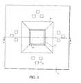
- FIG. 3is schematic drawing of a through-hole interconnection, top view in accordance with an exemplary embodiment of the present invention
- FIG. 4is a schematic drawing of a through-hole interconnection cross sectional view along line 4 — 4 shown in FIG. 3;
- FIG. 5 ( a )illustrates a cross-sectional view of a controlled impedance interconnect system and fabrication sequence in accordance with an exemplary embodiment of the present invention
- FIG. 5 ( b )illustrates a cross-sectional view of a controlled impedance interconnect system featuring interconnect wiring in accordance with an exemplary embodiment of the present invention
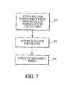
- FIG. 6illustrates the process for forming interconnect wiring between the signal Line wiring layer and substrate
- FIG. 7illustrates the process for forming interconnect wiring between the passive components and the signal line wiring layer
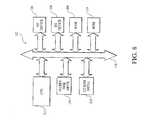
- FIG. 8illustrates a processor based system employing through-hole interconnections in accordance with an exemplary embodiment of the present invention.
- FIG. 2a chip carrier system in accordance with an exemplary embodiment of the present invention. It includes a chip carrier formed as a substrate 17 , e.g., a silicon substrate, on which passive or active circuit components 19 , such as resistors, capacitors, inductors, transistors, etc., can be formed, which is covered by a multi-layer wiring/insulation layer 15 (described in greater detail below), and on which a plurality of circuit chips are mounted. As illustrated in FIG.
- a substrate 17e.g., a silicon substrate
- passive or active circuit components 19such as resistors, capacitors, inductors, transistors, etc.
- the circuit chipsmay include one or more of a microprocessor chip 23 , DRAM chip 25 , SRAM chip 27 , ROM chip 24 , ASIC chip 28 , or other chips which are mounted to the multi-layer wiring/insulation layer 15 through a Ball Grid Array 13 .
- the chip carrieris also provided with one or more through-holes 29 through which the multi-layer wiring/insulation layer 15 passes to make electrical connection between chips mounted on opposite sides of the substrate 17 .
- only one through-hole 29is shown, but it should be understood that any number may be provided. Details of through-hole fabrication for a silicon substrate were given recently in C. Christensen, et al., “Wafer through-Hole Interconnections with High Vertical Wiring Densities,” IEEE Trans. On Components, Packing and Manufacturing Technology, Pt. A, vol. 19, no. 4, p. 516-522, 1996. Accordingly, a detailed description of how to form a through hole in substrate 17 will not be repeated herein.
- FIG. 3is a top view of a through-hole 29 of FIG. 2 with upper layers removed to show the signal line wiring layer 31 , which pass through the through-hole 29 and associated bond pads 33 which are connected to the signal line wiring layer 31 through interconnect wiring 60 (FIG. 4 ).
- a similar signal line wiring layer 31 and associated bond pads 33are provided on the opposite side of the substrate 17 .
- the through-holemay be a hollowed rectangle, circle, or any other geometric shape.
- the chips, supported by substrate 17are interconnected to input/output, ground and power terminals by virtue of their mounting on bond pads 33 .
- the through-hole 29 on the top surface illustrated in FIG. 3has sloping sidewalls 40 , as also illustrated in FIG. 2 .
- the through-hole 29 sizeis 1 mm square at its smallest opening dimension 22 (FIG. 2 ).
- FIG. 4is a cross sectional view along line 4 — 4 of FIG. 3 illustrating the detailed multi-layer wiring/insulation layer 15 .
- the multi-layer 15is formed on the substrate 17 , which may also have active and/or passive components 19 formed thereon.
- the multi-layer structureincludes a first insulating layer 35 , e.g., a silicon dioxide layer, formed as a continuous layer over both sides of substrate 17 and in the through-hole 29 , a first conductive ground plane layer 37 a or alternatively a conductive power supply distribution plane layer 37 b formed as a continuous layer over the first insulating layer 35 , a second insulating layer 39 formed as a continuous layer over the layer 37 a or 37 b , a signal line wiring layer 31 formed as a wiring pattern over the second insulating layer 39 , a third insulating layer 41 formed as a continuous layer over the signal line wiring layer 31 , another ground plane layer 43 a or alternatively another conductive power supply distribution plane layer 43 b formed as
- the signal line wiring layer 31is electrically connected to interconnect wiring 60 , 62 .
- the interconnect wiring 60electrically connects the signal lines of wiring layer 31 with bond pads 33 .
- the interconnect wiring 62electrically connects the active and/or passive structures formed on substrate 17 to the signal wiring layer 31 .
- the bond pads 33provide locations on which one or more of the chips 23 , 24 , 25 , 27 are mounted by for example, the Ball Grid Array technique, thereby electrically connecting the active and/or passive components fabricated on the substrate 17 to one or more of the chips 23 , 24 , 25 , 27 through wiring layer 31 .
- the chip carrier system illustrated in FIGS. 2-4contains short controlled impedance wiring paths between the chips mounted on both sides of substrate 17 through the multi-layer wiring/insulation layer 15 which passes through the through-hole 29 .
- FIG. 5 ( a )is a cross sectional view of a controlled impedance interconnect system of FIG. 4 showing the fabrication sequence.
- the first ground plane 37 a or the power supply distribution plane 37 bis first fabricated by depositing a highly conductive layer, such as copper or aluminum, by simple evaporation, sputtering or electroplating with a typical thickness of about 3 to 5 ⁇ m over a first insulating layer 35 , e.g. silicon dioxide, previously deposited over the substrate 17 by, for example, CVD, typically to a thickness of about 0.1 to 0.5 ⁇ m.
- a second insulating layer 39is deposited over this highly conductive layer 37 a or 37 b in step 2 .
- This second insulating layer 39preferably is silicon dioxide deposited by chemical vapor deposition (CVD) to a thickness of about 0.5 to 4 ⁇ m.
- CVDchemical vapor deposition
- the next stepis to fabricate the patterned signal lines 31 , which are typically about 6 to 10 ⁇ m wide, by employing optical lithography of a photoresist followed by additive metallization, such as liftoff by evaporation or electroplating, both of which are low-temperature processing techniques.
- a third insulating layer 41is deposited over the signal lines 31 .
- the third insulating layer 41is preferably a layer of silicon dioxide deposited by CVD to a thickness of at least 50% greater than the signal line wiring layer 31 conductor thickness to ensure good step coverage at the signal line 31 conductor corners. If a lower dielectric constant is desired, a lower dielectric constant polymer, such as polyimide, can be deposited by spin coating. In step 5 a planar conductor, as another ground plane 43 a or alternatively another conductive power supply distribution plane 43 b , is deposited over the third insulating layer 41 to a thickness of 3 to 5 ⁇ m as was done in step 1 .
- planarize the third insulating layer 41may also be desirable to planarize the third insulating layer 41 to provide a flat surface so that when planar conductor 43 a or 43 b is formed it is substantially planar.
- the final stepis to deposit a fourth insulating layer 45 over the planar conductor 43 a or 43 b.
- FIG. 5 ( b )illustrates a cross sectional view of the controlled impedance interconnect system of FIG. 5 ( a ) with the interconnect wiring 60 , 62 and bond pads 33 .
- FIGS. 6 and 7illustrate the steps needed to provide interconnect wiring 60 , 62 (FIG. 5 ( b )) between: (i) the active and/or passive components 19 formed on substrate 17 and the signal line wiring layer 31 and (ii) the signal line wiring layer 31 and the circuit chips 23 , 24 , 25 , 27 .
- interconnect wiring 62In order to get a signal from the active and/or passive components 19 to the signal lines 31 , interconnect wiring 62 , a signal conductor, must be fabricated. Materials and techniques for forming such interconnect wiring 62 are commonly known in the art. However, FIG. 6 provides a flow chart illustration of one exemplary technique in accordance with this invention. After step 2 of FIG. 5 ( a ) is completed, one or more holes are etched through the second insulating layer 39 , layers 37 a / 37 b and 35 to the active and/or passive components 19 . Based upon the size of interconnect wiring (conductor) 62 needed the hole may be formed by wet etching or dry etching, such as reactive ion or plasma etching, see step 502 .
- an hole insulator 72is deposited using CVD. This is to shield the soon to be deposited interconnect wiring 62 from the layers which are between the signal line wiring layer 31 and the substrate 17 .
- the hole insulator 72can be SiO 2 , Si 3 N 4 or other commonly known oxides.
- the interconnect wiring 62is deposited in step 506 .
- the interconnect wiringcan be aluminum or copper, for example.
- the interconnect wiring 62is deposited in the insulated hole by any commonly known process, e.g. evaporation, electroplating, etc.
- Step 506can occur at the same time as deposition of the signal wiring layer 31 (step 3 of FIG. 5 ( a )) in order to increase efficiency and attain maximum conductivity.
- the interconnect wiring 62is then used to carry a signal from the active and/or passive components 19 to the signal wiring layer 31 .
- FIG. 7illustrates a similar process as that described in FIG. 6 with the exception that FIG. 7 relates to depositing interconnect wiring 60 from the bond pads 33 of circuit chips 23 , 24 , 25 , 27 , 28 to the signal line wiring layer 31 .
- interconnect wiring 60one or more holes are etched in step 602 and a hole insulator 70 is deposited in step 604 as in the fabrication of interconnect wiring 62 .
- this processis performed after the deposition of the fourth insulating layer 45 (step 6 , FIG. 5 ( a )).
- the last stepagain, is to deposit the interconnect wiring 62 in step 606 .
- the bonds pads 33may all be fabricated in a one step metallization to increase efficiency and conductivity.
- the substrate 17 with multi-layer wiring/insulation layer 15 and associated circuit chips 23 , 24 , 25 , 27 , 28may all be encapsulated in a single integrated package unit composed of a plastic composite. In such an implementation multiple exterior pins are needed to interface the integrated package unit to a circuit board for communication with other components of a system.
- FIG. 8illustrates a processor-based system 102 , including central processing unit (CPU) 112 , memory devices 108 , 110 , input/output (I/O) devices 104 , 106 , floppy disk drive 114 and CD ROM drive 116 . All of the above components communicate with each other over bus 118 .
- the central processing unit (CPU) 112 , and one or more of the memory devices 108 , 110are fabricated as one or more chips which can be mounted onto a chip carrier 17 , as illustrated in FIG. 2, with through-hole interconnections in accordance with the present invention as described above.
- the present inventionprovides for an apparatus and method of making the same which results in a chip carrier system with short through-hole interconnections and with a low impedance.
- the conducting and insulting layerscan be constructed of many different commonly known materials.
- alternative insulating and conducting layerscan be formed within the multi-layer wiring/insulating layer 15 and any number of conductive and insulating layers can be used.
Landscapes
- Engineering & Computer Science (AREA)
- Microelectronics & Electronic Packaging (AREA)
- Physics & Mathematics (AREA)
- Condensed Matter Physics & Semiconductors (AREA)
- General Physics & Mathematics (AREA)
- Computer Hardware Design (AREA)
- Power Engineering (AREA)
- Internal Circuitry In Semiconductor Integrated Circuit Devices (AREA)
- Semiconductor Integrated Circuits (AREA)
Abstract
Description
Claims (85)
Priority Applications (4)
| Application Number | Priority Date | Filing Date | Title |
|---|---|---|---|
| US09/517,318US6441479B1 (en) | 2000-03-02 | 2000-03-02 | System-on-a-chip with multi-layered metallized through-hole interconnection |
| US10/191,277US6962866B2 (en) | 2000-03-02 | 2002-07-10 | System-on-a-chip with multi-layered metallized through-hole interconnection |
| US10/784,233US6984886B2 (en) | 2000-03-02 | 2004-02-24 | System-on-a-chip with multi-layered metallized through-hole interconnection |
| US11/248,144US7294921B2 (en) | 2000-03-02 | 2005-10-13 | System-on-a-chip with multi-layered metallized through-hole interconnection |
Applications Claiming Priority (1)
| Application Number | Priority Date | Filing Date | Title |
|---|---|---|---|
| US09/517,318US6441479B1 (en) | 2000-03-02 | 2000-03-02 | System-on-a-chip with multi-layered metallized through-hole interconnection |
Related Child Applications (1)
| Application Number | Title | Priority Date | Filing Date |
|---|---|---|---|
| US10/191,277DivisionUS6962866B2 (en) | 2000-03-02 | 2002-07-10 | System-on-a-chip with multi-layered metallized through-hole interconnection |
Publications (1)
| Publication Number | Publication Date |
|---|---|
| US6441479B1true US6441479B1 (en) | 2002-08-27 |
Family
ID=24059310
Family Applications (4)
| Application Number | Title | Priority Date | Filing Date |
|---|---|---|---|
| US09/517,318Expired - LifetimeUS6441479B1 (en) | 2000-03-02 | 2000-03-02 | System-on-a-chip with multi-layered metallized through-hole interconnection |
| US10/191,277Expired - Fee RelatedUS6962866B2 (en) | 2000-03-02 | 2002-07-10 | System-on-a-chip with multi-layered metallized through-hole interconnection |
| US10/784,233Expired - Fee RelatedUS6984886B2 (en) | 2000-03-02 | 2004-02-24 | System-on-a-chip with multi-layered metallized through-hole interconnection |
| US11/248,144Expired - LifetimeUS7294921B2 (en) | 2000-03-02 | 2005-10-13 | System-on-a-chip with multi-layered metallized through-hole interconnection |
Family Applications After (3)
| Application Number | Title | Priority Date | Filing Date |
|---|---|---|---|
| US10/191,277Expired - Fee RelatedUS6962866B2 (en) | 2000-03-02 | 2002-07-10 | System-on-a-chip with multi-layered metallized through-hole interconnection |
| US10/784,233Expired - Fee RelatedUS6984886B2 (en) | 2000-03-02 | 2004-02-24 | System-on-a-chip with multi-layered metallized through-hole interconnection |
| US11/248,144Expired - LifetimeUS7294921B2 (en) | 2000-03-02 | 2005-10-13 | System-on-a-chip with multi-layered metallized through-hole interconnection |
Country Status (1)
| Country | Link |
|---|---|
| US (4) | US6441479B1 (en) |
Cited By (25)
| Publication number | Priority date | Publication date | Assignee | Title |
|---|---|---|---|---|
| US20020113322A1 (en)* | 2000-06-12 | 2002-08-22 | Shinichi Terashima | Semiconductor device and method to produce the same |
| US20020185730A1 (en)* | 2000-03-02 | 2002-12-12 | Ahn Kie Y. | System-on-a-chip with multi-layered metallized through-hole interconnection |
| US20030200654A1 (en)* | 2002-04-25 | 2003-10-30 | Fujitsu Limited | Method of manufacturing electronic circuit component |
| US20040019841A1 (en)* | 2002-07-25 | 2004-01-29 | Ong Adrian E. | Internally generating patterns for testing in an integrated circuit device |
| US6727533B2 (en)* | 2000-11-29 | 2004-04-27 | Fujitsu Limited | Semiconductor apparatus having a large-size bus connection |
| US6732304B1 (en) | 2000-09-21 | 2004-05-04 | Inapac Technology, Inc. | Chip testing within a multi-chip semiconductor package |
| US6754866B1 (en) | 2001-09-28 | 2004-06-22 | Inapac Technology, Inc. | Testing of integrated circuit devices |
| US20040173909A1 (en)* | 2003-03-05 | 2004-09-09 | Micron Technology, Inc. | Conductive through wafer vias |
| US6812726B1 (en) | 2002-11-27 | 2004-11-02 | Inapac Technology, Inc. | Entering test mode and accessing of a packaged semiconductor device |
| US20050024977A1 (en)* | 2000-09-21 | 2005-02-03 | Ong Adrian E. | Multiple power levels for a chip within a multi-chip semiconductor package |
| US20050146049A1 (en)* | 2003-12-24 | 2005-07-07 | Agency For Science, Technology And Research | RF and MMIC stackable micro-modules |
| US20050162182A1 (en)* | 2002-07-25 | 2005-07-28 | Ong Adrian E. | Internally generating patterns for testing in an integrated circuit device |
| US20050223147A1 (en)* | 2004-03-19 | 2005-10-06 | Infineon Technologies Ag | Method and apparatus for allocating bus access rights in multimaster bus systems |
| US20050250247A1 (en)* | 2004-05-04 | 2005-11-10 | Semikron Elektronik Gmbh | Method for internal electrical insulation of a substrate for a power semiconductor module |
| US20050289428A1 (en)* | 2000-09-21 | 2005-12-29 | Sidley Austin Brown & Wood Llp | Architecture and method for testing of an integrated circuit device |
| US7061263B1 (en) | 2001-11-15 | 2006-06-13 | Inapac Technology, Inc. | Layout and use of bond pads and probe pads for testing of integrated circuits devices |
| US20060179192A1 (en)* | 2005-02-10 | 2006-08-10 | Ganasan J Prakash S | Flow control method to improve bus utilization in a system-on-a-chip integrated circuit |
| US20070079204A1 (en)* | 2001-09-28 | 2007-04-05 | Ong Adrian E | Integrated Circuit Testing Module Including Signal Shaping Interface |
| US7466603B2 (en) | 2006-10-03 | 2008-12-16 | Inapac Technology, Inc. | Memory accessing circuit system |
| US20090273098A1 (en)* | 2008-05-01 | 2009-11-05 | Gerald Keith Bartley | Enhanced Architectural Interconnect Options Enabled With Flipped Die on a Multi-Chip Package |
| US8063650B2 (en) | 2002-11-27 | 2011-11-22 | Rambus Inc. | Testing fuse configurations in semiconductor devices |
| US8166361B2 (en) | 2001-09-28 | 2012-04-24 | Rambus Inc. | Integrated circuit testing module configured for set-up and hold time testing |
| US8286046B2 (en) | 2001-09-28 | 2012-10-09 | Rambus Inc. | Integrated circuit testing module including signal shaping interface |
| USD728577S1 (en)* | 2014-07-01 | 2015-05-05 | Google Inc. | Mobile device module |
| USD730906S1 (en)* | 2014-07-01 | 2015-06-02 | Google Inc. | Mobile device module |
Families Citing this family (28)
| Publication number | Priority date | Publication date | Assignee | Title |
|---|---|---|---|---|
| US6576484B1 (en)* | 2001-05-23 | 2003-06-10 | Advanced Micro Devices, Inc. | IC die analysis via back side circuit construction with heat dissipation |
| JP3862633B2 (en)* | 2002-08-14 | 2006-12-27 | 東京エレクトロン株式会社 | Method for manufacturing non-radiative dielectric line |
| JP2004079701A (en)* | 2002-08-14 | 2004-03-11 | Sony Corp | Semiconductor device and its manufacturing method |
| US7265300B2 (en)* | 2003-03-21 | 2007-09-04 | Commscope Solutions Properties, Llc | Next high frequency improvement using hybrid substrates of two materials with different dielectric constant frequency slopes |
| US7182738B2 (en) | 2003-04-23 | 2007-02-27 | Marctec, Llc | Patient monitoring apparatus and method for orthosis and other devices |
| DE10319538B4 (en)* | 2003-04-30 | 2008-01-17 | Qimonda Ag | Semiconductor device and method for producing a semiconductor device |
| US7342181B2 (en)* | 2004-03-12 | 2008-03-11 | Commscope Inc. Of North Carolina | Maximizing capacitance per unit area while minimizing signal transmission delay in PCB |
| US7980900B2 (en)* | 2004-05-14 | 2011-07-19 | Commscope, Inc. Of North Carolina | Next high frequency improvement by using frequency dependent effective capacitance |
| US7190594B2 (en)* | 2004-05-14 | 2007-03-13 | Commscope Solutions Properties, Llc | Next high frequency improvement by using frequency dependent effective capacitance |
| US7307022B2 (en)* | 2004-11-19 | 2007-12-11 | Endicott Interconnect Technologies, Inc. | Method of treating conductive layer for use in a circuitized substrate and method of making said substrate having said conductive layer as part thereof |
| WO2008003051A2 (en)* | 2006-06-29 | 2008-01-03 | Analog Devices, Inc. | Stress mitigation in packaged microchips |
| JPWO2008105149A1 (en)* | 2007-02-26 | 2010-06-03 | 日本電気株式会社 | Circuit module |
| US7694610B2 (en)* | 2007-06-27 | 2010-04-13 | Siemens Medical Solutions Usa, Inc. | Photo-multiplier tube removal tool |
| US20100159193A1 (en)* | 2008-12-18 | 2010-06-24 | Palo Alto Research Center Incorporated | Combined electrical and fluidic interconnect via structure |
| US8047879B2 (en)* | 2009-01-26 | 2011-11-01 | Commscope, Inc. Of North Carolina | Printed wiring boards and communication connectors having series inductor-capacitor crosstalk compensation circuits that share a common inductor |
| JP5147779B2 (en) | 2009-04-16 | 2013-02-20 | 新光電気工業株式会社 | Wiring board manufacturing method and semiconductor package manufacturing method |
| KR101276333B1 (en)* | 2009-11-30 | 2013-06-18 | 한국전자통신연구원 | 3d interconnection structure and manufacturing method thereof |
| US8847380B2 (en)* | 2010-09-17 | 2014-09-30 | Tessera, Inc. | Staged via formation from both sides of chip |
| US8575558B2 (en) | 2010-11-30 | 2013-11-05 | General Electric Company | Detector array with a through-via interposer |
| US8446275B2 (en) | 2011-06-10 | 2013-05-21 | Aliphcom | General health and wellness management method and apparatus for a wellness application using data from a data-capable band |
| US9258670B2 (en) | 2011-06-10 | 2016-02-09 | Aliphcom | Wireless enabled cap for a data-capable device |
| US9069380B2 (en) | 2011-06-10 | 2015-06-30 | Aliphcom | Media device, application, and content management using sensory input |
| US20120313296A1 (en)* | 2011-06-10 | 2012-12-13 | Aliphcom | Component protective overmolding |
| US9676614B2 (en) | 2013-02-01 | 2017-06-13 | Analog Devices, Inc. | MEMS device with stress relief structures |
| US10167189B2 (en) | 2014-09-30 | 2019-01-01 | Analog Devices, Inc. | Stress isolation platform for MEMS devices |
| US10131538B2 (en) | 2015-09-14 | 2018-11-20 | Analog Devices, Inc. | Mechanically isolated MEMS device |
| US11417611B2 (en) | 2020-02-25 | 2022-08-16 | Analog Devices International Unlimited Company | Devices and methods for reducing stress on circuit components |
| US11981560B2 (en) | 2020-06-09 | 2024-05-14 | Analog Devices, Inc. | Stress-isolated MEMS device comprising substrate having cavity and method of manufacture |
Citations (10)
| Publication number | Priority date | Publication date | Assignee | Title |
|---|---|---|---|---|
| US3602635A (en)* | 1970-06-30 | 1971-08-31 | Ibm | Micro-circuit device |
| US3673680A (en)* | 1970-12-14 | 1972-07-04 | California Computer Products | Method of circuit board with solder coated pattern |
| US3934335A (en)* | 1974-10-16 | 1976-01-27 | Texas Instruments Incorporated | Multilayer printed circuit board |
| US4188415A (en)* | 1976-09-14 | 1980-02-12 | Hitachi Chemical Company, Ltd. | Baseboard for printed circuit board and method of producing the same |
| US4303715A (en)* | 1977-04-07 | 1981-12-01 | Western Electric Company, Incorporated | Printed wiring board |
| US5153986A (en)* | 1991-07-17 | 1992-10-13 | International Business Machines | Method for fabricating metal core layers for a multi-layer circuit board |
| JPH05144221A (en)* | 1991-11-22 | 1993-06-11 | Sony Corp | Disk cartridge |
| US5502893A (en)* | 1992-10-09 | 1996-04-02 | International Business Machines Corporation | Method of making a printing wiring board |
| US5557142A (en)* | 1991-02-04 | 1996-09-17 | Motorola, Inc. | Shielded semiconductor device package |
| US5587885A (en)* | 1994-05-18 | 1996-12-24 | Dell Usa, L.P. | Mechanical printed circuit board/laminated multi chip module interconnect apparatus |
Family Cites Families (23)
| Publication number | Priority date | Publication date | Assignee | Title |
|---|---|---|---|---|
| US3334395A (en)* | 1962-11-26 | 1967-08-08 | Northrop Corp | Method of making a metal printed circuit board |
| US3317408A (en)* | 1963-06-11 | 1967-05-02 | North American Aviation Inc | Method of making a magnetic core storage device |
| US3322881A (en)* | 1964-08-19 | 1967-05-30 | Jr Frederick W Schneble | Multilayer printed circuit assemblies |
| US3739469A (en)* | 1971-12-27 | 1973-06-19 | Ibm | Multilayer printed circuit board and method of manufacture |
| US3763680A (en)* | 1972-08-23 | 1973-10-09 | Cf & I Steel Corp | Method and apparatus for treating wire |
| US3934334A (en)* | 1974-04-15 | 1976-01-27 | Texas Instruments Incorporated | Method of fabricating metal printed wiring boards |
| US4582564A (en)* | 1982-01-04 | 1986-04-15 | At&T Technologies, Inc. | Method of providing an adherent metal coating on an epoxy surface |
| US5089881A (en)* | 1988-11-03 | 1992-02-18 | Micro Substrates, Inc. | Fine-pitch chip carrier |
| JP2925609B2 (en) | 1989-11-30 | 1999-07-28 | 沖電気工業株式会社 | Method for manufacturing semiconductor device |
| US5487214A (en)* | 1991-07-10 | 1996-01-30 | International Business Machines Corp. | Method of making a monolithic magnetic device with printed circuit interconnections |
| KR960006961B1 (en)* | 1991-09-13 | 1996-05-25 | 니뽄 덴끼 가부시끼가이샤 | Wiring structure and insulating film formation method of semiconductor device and surface protection film formation method thereof |
| US5272600A (en)* | 1992-09-02 | 1993-12-21 | Microelectronics And Computer Technology Corporation | Electrical interconnect device with interwoven power and ground lines and capacitive vias |
| US5421083A (en)* | 1994-04-01 | 1995-06-06 | Motorola, Inc. | Method of manufacturing a circuit carrying substrate having coaxial via holes |
| US5876842A (en)* | 1995-06-07 | 1999-03-02 | International Business Machines Corporation | Modular circuit package having vertically aligned power and signal cores |
| US5689091A (en)* | 1996-09-19 | 1997-11-18 | Vlsi Technology, Inc. | Multi-layer substrate structure |
| US5811868A (en)* | 1996-12-20 | 1998-09-22 | International Business Machines Corp. | Integrated high-performance decoupling capacitor |
| US5949030A (en)* | 1997-11-14 | 1999-09-07 | International Business Machines Corporation | Vias and method for making the same in organic board and chip carriers |
| JP3218024B2 (en)* | 1998-05-22 | 2001-10-15 | セイコーインスツルメンツ株式会社 | Method and apparatus for forming metal pattern film |
| US6246112B1 (en)* | 1998-06-11 | 2001-06-12 | Intel Corporation | Interleaved signal trace routing |
| US6320244B1 (en)* | 1999-01-12 | 2001-11-20 | Agere Systems Guardian Corp. | Integrated circuit device having dual damascene capacitor |
| TW411737B (en)* | 1999-03-09 | 2000-11-11 | Unimicron Technology Corp | A 2-stage process to form micro via |
| US6441479B1 (en)* | 2000-03-02 | 2002-08-27 | Micron Technology, Inc. | System-on-a-chip with multi-layered metallized through-hole interconnection |
| US6617526B2 (en)* | 2001-04-23 | 2003-09-09 | Lockheed Martin Corporation | UHF ground interconnects |
- 2000
- 2000-03-02USUS09/517,318patent/US6441479B1/ennot_activeExpired - Lifetime
- 2002
- 2002-07-10USUS10/191,277patent/US6962866B2/ennot_activeExpired - Fee Related
- 2004
- 2004-02-24USUS10/784,233patent/US6984886B2/ennot_activeExpired - Fee Related
- 2005
- 2005-10-13USUS11/248,144patent/US7294921B2/ennot_activeExpired - Lifetime
Patent Citations (10)
| Publication number | Priority date | Publication date | Assignee | Title |
|---|---|---|---|---|
| US3602635A (en)* | 1970-06-30 | 1971-08-31 | Ibm | Micro-circuit device |
| US3673680A (en)* | 1970-12-14 | 1972-07-04 | California Computer Products | Method of circuit board with solder coated pattern |
| US3934335A (en)* | 1974-10-16 | 1976-01-27 | Texas Instruments Incorporated | Multilayer printed circuit board |
| US4188415A (en)* | 1976-09-14 | 1980-02-12 | Hitachi Chemical Company, Ltd. | Baseboard for printed circuit board and method of producing the same |
| US4303715A (en)* | 1977-04-07 | 1981-12-01 | Western Electric Company, Incorporated | Printed wiring board |
| US5557142A (en)* | 1991-02-04 | 1996-09-17 | Motorola, Inc. | Shielded semiconductor device package |
| US5153986A (en)* | 1991-07-17 | 1992-10-13 | International Business Machines | Method for fabricating metal core layers for a multi-layer circuit board |
| JPH05144221A (en)* | 1991-11-22 | 1993-06-11 | Sony Corp | Disk cartridge |
| US5502893A (en)* | 1992-10-09 | 1996-04-02 | International Business Machines Corporation | Method of making a printing wiring board |
| US5587885A (en)* | 1994-05-18 | 1996-12-24 | Dell Usa, L.P. | Mechanical printed circuit board/laminated multi chip module interconnect apparatus |
Non-Patent Citations (6)
| Title |
|---|
| Carsten Christensen et al, "Wafer Through-Hole Interconnections with High Vertical Wiring Densities," IEEE Transactions on Components . . . , Part A, vol. 19, No. 4, Dec. 1996; pp. 516-522. |
| Evan E. Davidson et al, "Long Lossy Lines (L3) and Their Impact Upon Large Chip Performance," IEEE Transactions . . . , Part B, vol. 20, No. 4, Nov. 1997, pp. 361-375. |
| Michael Gribbons et al., "Finite-Difference Time-Domain Analysis of Pulse Propagation in Multichip Module Interconnects," IEEE Transactions of Components . . . vol. 16, No. 5, 1993; pp. 490497. |
| R. Downing et al., "Decoupling Capacitor Effects on Switching Noise," IEEE Transactions of Components . . . , vol. 16, No. 5, 1993 pp. 484-489. |
| R. J. Jensen, "Designing for Reliability in Harsh Environments," MCM technology, Honeywell Solid State Electronics Center 1997. |
| T. Mimura et al., "System Module: A New Chip-on-Chip Module Technology," Semiconductor Research Center, Matsushita Electrical Industrial Co., Ltd., pp. 21.5.1-21.5.4. |
Cited By (65)
| Publication number | Priority date | Publication date | Assignee | Title |
|---|---|---|---|---|
| US7294921B2 (en)* | 2000-03-02 | 2007-11-13 | Micron Technology, Inc. | System-on-a-chip with multi-layered metallized through-hole interconnection |
| US6984886B2 (en)* | 2000-03-02 | 2006-01-10 | Micron Technology, Inc. | System-on-a-chip with multi-layered metallized through-hole interconnection |
| US20040164398A1 (en)* | 2000-03-02 | 2004-08-26 | Ahn Kie Y. | System-on-a-chip with multi-layered metallized through-hole interconnection |
| US6962866B2 (en) | 2000-03-02 | 2005-11-08 | Micron Technology, Inc. | System-on-a-chip with multi-layered metallized through-hole interconnection |
| US20060038279A1 (en)* | 2000-03-02 | 2006-02-23 | Ahn Kie Y | System-on-a-chip with multi-layered metallized through-hole interconnection |
| US20020185730A1 (en)* | 2000-03-02 | 2002-12-12 | Ahn Kie Y. | System-on-a-chip with multi-layered metallized through-hole interconnection |
| US20020113322A1 (en)* | 2000-06-12 | 2002-08-22 | Shinichi Terashima | Semiconductor device and method to produce the same |
| US7444575B2 (en) | 2000-09-21 | 2008-10-28 | Inapac Technology, Inc. | Architecture and method for testing of an integrated circuit device |
| US20050289428A1 (en)* | 2000-09-21 | 2005-12-29 | Sidley Austin Brown & Wood Llp | Architecture and method for testing of an integrated circuit device |
| US6732304B1 (en) | 2000-09-21 | 2004-05-04 | Inapac Technology, Inc. | Chip testing within a multi-chip semiconductor package |
| US20040196709A1 (en)* | 2000-09-21 | 2004-10-07 | Ong Adrian E. | Chip testing within a multi-chip semiconductor package |
| US7139945B2 (en) | 2000-09-21 | 2006-11-21 | Inapac Technology, Inc. | Chip testing within a multi-chip semiconductor package |
| US7240254B2 (en) | 2000-09-21 | 2007-07-03 | Inapac Technology, Inc | Multiple power levels for a chip within a multi-chip semiconductor package |
| US20050024977A1 (en)* | 2000-09-21 | 2005-02-03 | Ong Adrian E. | Multiple power levels for a chip within a multi-chip semiconductor package |
| US20040188718A1 (en)* | 2000-11-29 | 2004-09-30 | Fujitsu Limited | Semiconductor apparatus having a large-size bus connection |
| US7317241B2 (en) | 2000-11-29 | 2008-01-08 | Fujitsu Limited | Semiconductor apparatus having a large-size bus connection |
| US6727533B2 (en)* | 2000-11-29 | 2004-04-27 | Fujitsu Limited | Semiconductor apparatus having a large-size bus connection |
| US20080142847A1 (en)* | 2000-11-29 | 2008-06-19 | Fujitsu Limited | Semiconductor apparatus having a large-size bus connection |
| US6936874B2 (en) | 2000-11-29 | 2005-08-30 | Fujitsu Limited | Semiconductor apparatus having a large-size bus connection |
| US20050218432A1 (en)* | 2000-11-29 | 2005-10-06 | Fujitsu Limited | Semiconductor apparatus having a large-size bus connection |
| US7907434B2 (en) | 2000-11-29 | 2011-03-15 | Fujitsu Semiconductor Limited | Semiconductor apparatus having a large-size bus connection |
| US8286046B2 (en) | 2001-09-28 | 2012-10-09 | Rambus Inc. | Integrated circuit testing module including signal shaping interface |
| US8166361B2 (en) | 2001-09-28 | 2012-04-24 | Rambus Inc. | Integrated circuit testing module configured for set-up and hold time testing |
| US9116210B2 (en) | 2001-09-28 | 2015-08-25 | Rambus Inc. | Integrated circuit testing module including signal shaping interface |
| US20070079204A1 (en)* | 2001-09-28 | 2007-04-05 | Ong Adrian E | Integrated Circuit Testing Module Including Signal Shaping Interface |
| US20040225937A1 (en)* | 2001-09-28 | 2004-11-11 | Ong Adrian E. | Testing of integrated circuit devices |
| US10114073B2 (en) | 2001-09-28 | 2018-10-30 | Rambus Inc. | Integrated circuit testing |
| US8001439B2 (en) | 2001-09-28 | 2011-08-16 | Rambus Inc. | Integrated circuit testing module including signal shaping interface |
| US7103815B2 (en) | 2001-09-28 | 2006-09-05 | Inapac Technology, Inc. | Testing of integrated circuit devices |
| US6754866B1 (en) | 2001-09-28 | 2004-06-22 | Inapac Technology, Inc. | Testing of integrated circuit devices |
| US7061263B1 (en) | 2001-11-15 | 2006-06-13 | Inapac Technology, Inc. | Layout and use of bond pads and probe pads for testing of integrated circuits devices |
| US6979644B2 (en)* | 2002-04-25 | 2005-12-27 | Fujitsu Limited | Method of manufacturing electronic circuit component |
| US20030200654A1 (en)* | 2002-04-25 | 2003-10-30 | Fujitsu Limited | Method of manufacturing electronic circuit component |
| US20040019841A1 (en)* | 2002-07-25 | 2004-01-29 | Ong Adrian E. | Internally generating patterns for testing in an integrated circuit device |
| US20050162182A1 (en)* | 2002-07-25 | 2005-07-28 | Ong Adrian E. | Internally generating patterns for testing in an integrated circuit device |
| US7313740B2 (en) | 2002-07-25 | 2007-12-25 | Inapac Technology, Inc. | Internally generating patterns for testing in an integrated circuit device |
| US6882171B2 (en) | 2002-11-27 | 2005-04-19 | Inapac Technology, Inc. | Bonding pads for testing of a semiconductor device |
| US6812726B1 (en) | 2002-11-27 | 2004-11-02 | Inapac Technology, Inc. | Entering test mode and accessing of a packaged semiconductor device |
| US11009548B2 (en) | 2002-11-27 | 2021-05-18 | Rambus Inc. | Testing fuse configurations in semiconductor devices |
| US20050204223A1 (en)* | 2002-11-27 | 2005-09-15 | Ong Adrian E. | Bonding pads for testing of a semiconductor device |
| US10302696B2 (en) | 2002-11-27 | 2019-05-28 | Rambus Inc. | Testing fuse configurations in semiconductor devices |
| US8063650B2 (en) | 2002-11-27 | 2011-11-22 | Rambus Inc. | Testing fuse configurations in semiconductor devices |
| US9568544B2 (en) | 2002-11-27 | 2017-02-14 | Rambus Inc. | Testing fuse configurations in semiconductor devices |
| US8717052B2 (en) | 2002-11-27 | 2014-05-06 | Rambus Inc. | Testing fuse configurations in semiconductor devices |
| US7259582B2 (en) | 2002-11-27 | 2007-08-21 | Inapac Technology, Inc. | Bonding pads for testing of a semiconductor device |
| US20050200027A1 (en)* | 2003-03-05 | 2005-09-15 | Micron Technology, Inc. | Conductive through wafer vias |
| US6852627B2 (en) | 2003-03-05 | 2005-02-08 | Micron Technology, Inc. | Conductive through wafer vias |
| US20040173909A1 (en)* | 2003-03-05 | 2004-09-09 | Micron Technology, Inc. | Conductive through wafer vias |
| US20050146049A1 (en)* | 2003-12-24 | 2005-07-07 | Agency For Science, Technology And Research | RF and MMIC stackable micro-modules |
| US7230318B2 (en)* | 2003-12-24 | 2007-06-12 | Agency For Science, Technology And Research | RF and MMIC stackable micro-modules |
| US20050223147A1 (en)* | 2004-03-19 | 2005-10-06 | Infineon Technologies Ag | Method and apparatus for allocating bus access rights in multimaster bus systems |
| US7373445B2 (en)* | 2004-03-19 | 2008-05-13 | Infineon Technologies Ag | Method and apparatus for allocating bus access rights in multimaster bus systems |
| US7723244B2 (en)* | 2004-05-04 | 2010-05-25 | Semikron Elektronik Gmbh & Co. Kg | Method for internal electrical insulation of a substrate for a power semiconductor module |
| US20050250247A1 (en)* | 2004-05-04 | 2005-11-10 | Semikron Elektronik Gmbh | Method for internal electrical insulation of a substrate for a power semiconductor module |
| JP2008530694A (en)* | 2005-02-10 | 2008-08-07 | クゥアルコム・インコーポレイテッド | Flow control method to improve data transfer via switch matrix |
| JP2011048838A (en)* | 2005-02-10 | 2011-03-10 | Qualcomm Inc | Flow control method for improving data transfer via switch matrix |
| JP2012038325A (en)* | 2005-02-10 | 2012-02-23 | Qualcomm Inc | Flow control method to improve data transmission via switch matrix |
| JP4861339B2 (en)* | 2005-02-10 | 2012-01-25 | クゥアルコム・インコーポレイテッド | Flow control method to improve data transfer via switch matrix |
| US20060179192A1 (en)* | 2005-02-10 | 2006-08-10 | Ganasan J Prakash S | Flow control method to improve bus utilization in a system-on-a-chip integrated circuit |
| US7246188B2 (en)* | 2005-02-10 | 2007-07-17 | Qualcomm Incorporated | Flow control method to improve bus utilization in a system-on-a-chip integrated circuit |
| US7466603B2 (en) | 2006-10-03 | 2008-12-16 | Inapac Technology, Inc. | Memory accessing circuit system |
| US8174103B2 (en)* | 2008-05-01 | 2012-05-08 | International Business Machines Corporation | Enhanced architectural interconnect options enabled with flipped die on a multi-chip package |
| US20090273098A1 (en)* | 2008-05-01 | 2009-11-05 | Gerald Keith Bartley | Enhanced Architectural Interconnect Options Enabled With Flipped Die on a Multi-Chip Package |
| USD728577S1 (en)* | 2014-07-01 | 2015-05-05 | Google Inc. | Mobile device module |
| USD730906S1 (en)* | 2014-07-01 | 2015-06-02 | Google Inc. | Mobile device module |
Also Published As
| Publication number | Publication date |
|---|---|
| US6962866B2 (en) | 2005-11-08 |
| US6984886B2 (en) | 2006-01-10 |
| US7294921B2 (en) | 2007-11-13 |
| US20060038279A1 (en) | 2006-02-23 |
| US20020185730A1 (en) | 2002-12-12 |
| US20040164398A1 (en) | 2004-08-26 |
Similar Documents
| Publication | Publication Date | Title |
|---|---|---|
| US6441479B1 (en) | System-on-a-chip with multi-layered metallized through-hole interconnection | |
| CN112687659B (en) | Semiconductor structure and method for forming semiconductor structure | |
| KR100656218B1 (en) | Systems on Packages Fabricated on Semiconductor or Dielectric Wafers | |
| US4866507A (en) | Module for packaging semiconductor integrated circuit chips on a base substrate | |
| US5424245A (en) | Method of forming vias through two-sided substrate | |
| US6222276B1 (en) | Through-chip conductors for low inductance chip-to-chip integration and off-chip connections | |
| KR100552551B1 (en) | High Performance Silicon Contacts for Flip Chip | |
| US5935687A (en) | Three dimensional package and architecture for high performance computer | |
| US6570248B1 (en) | Structure and method for a high-performance electronic packaging assembly | |
| KR101452548B1 (en) | Semiconductor die with backside passive device integration | |
| US8937389B2 (en) | Semiconductor devices comprising GSG interconnect structures | |
| US20040072422A1 (en) | Methods of forming conductive through-wafer vias | |
| US5134539A (en) | Multichip module having integral decoupling capacitor | |
| US9653586B2 (en) | Amplifier device comprising enhanced thermal transfer and structural features | |
| US20050253278A1 (en) | Universal interconnect die | |
| WO2007050754A2 (en) | Stackable wafer or die packaging with enhanced thermal and device performance | |
| US5274270A (en) | Multichip module having SiO2 insulating layer | |
| WO2023038647A1 (en) | Power routing for 2.5d or 3d integrated circuits | |
| US5914533A (en) | Multilayer module with thinfilm redistribution area | |
| CN113990852A (en) | Antenna device and manufacturing method | |
| US6670703B1 (en) | Buried ground plane for high performance system modules | |
| US5214844A (en) | Method of assembling integrated circuits to a silicon board | |
| US20230130354A1 (en) | Three-dimensional semiconductor package having a stacked passive device | |
| JP2001035993A (en) | Multi-chip module and manufacture thereof | |
| US20250054867A1 (en) | Fan-out package including bridge structure and method of manufacturing the same |
Legal Events
| Date | Code | Title | Description |
|---|---|---|---|
| AS | Assignment | Owner name:MICRON TECHNOLOGY, INC., IDAHO Free format text:ASSIGNMENT OF ASSIGNORS INTEREST;ASSIGNORS:AHN, KIE Y.;FORBES, LEONARD;REEL/FRAME:010601/0250;SIGNING DATES FROM 20000224 TO 20000225 | |
| STCF | Information on status: patent grant | Free format text:PATENTED CASE | |
| FEPP | Fee payment procedure | Free format text:PAYER NUMBER DE-ASSIGNED (ORIGINAL EVENT CODE: RMPN); ENTITY STATUS OF PATENT OWNER: LARGE ENTITY Free format text:PAYOR NUMBER ASSIGNED (ORIGINAL EVENT CODE: ASPN); ENTITY STATUS OF PATENT OWNER: LARGE ENTITY | |
| FPAY | Fee payment | Year of fee payment:4 | |
| FPAY | Fee payment | Year of fee payment:8 | |
| FPAY | Fee payment | Year of fee payment:12 | |
| AS | Assignment | Owner name:U.S. BANK NATIONAL ASSOCIATION, AS COLLATERAL AGENT, CALIFORNIA Free format text:SECURITY INTEREST;ASSIGNOR:MICRON TECHNOLOGY, INC.;REEL/FRAME:038669/0001 Effective date:20160426 Owner name:U.S. BANK NATIONAL ASSOCIATION, AS COLLATERAL AGEN Free format text:SECURITY INTEREST;ASSIGNOR:MICRON TECHNOLOGY, INC.;REEL/FRAME:038669/0001 Effective date:20160426 | |
| AS | Assignment | Owner name:MORGAN STANLEY SENIOR FUNDING, INC., AS COLLATERAL AGENT, MARYLAND Free format text:PATENT SECURITY AGREEMENT;ASSIGNOR:MICRON TECHNOLOGY, INC.;REEL/FRAME:038954/0001 Effective date:20160426 Owner name:MORGAN STANLEY SENIOR FUNDING, INC., AS COLLATERAL Free format text:PATENT SECURITY AGREEMENT;ASSIGNOR:MICRON TECHNOLOGY, INC.;REEL/FRAME:038954/0001 Effective date:20160426 | |
| AS | Assignment | Owner name:U.S. BANK NATIONAL ASSOCIATION, AS COLLATERAL AGENT, CALIFORNIA Free format text:CORRECTIVE ASSIGNMENT TO CORRECT THE REPLACE ERRONEOUSLY FILED PATENT #7358718 WITH THE CORRECT PATENT #7358178 PREVIOUSLY RECORDED ON REEL 038669 FRAME 0001. ASSIGNOR(S) HEREBY CONFIRMS THE SECURITY INTEREST;ASSIGNOR:MICRON TECHNOLOGY, INC.;REEL/FRAME:043079/0001 Effective date:20160426 Owner name:U.S. BANK NATIONAL ASSOCIATION, AS COLLATERAL AGEN Free format text:CORRECTIVE ASSIGNMENT TO CORRECT THE REPLACE ERRONEOUSLY FILED PATENT #7358718 WITH THE CORRECT PATENT #7358178 PREVIOUSLY RECORDED ON REEL 038669 FRAME 0001. ASSIGNOR(S) HEREBY CONFIRMS THE SECURITY INTEREST;ASSIGNOR:MICRON TECHNOLOGY, INC.;REEL/FRAME:043079/0001 Effective date:20160426 | |
| AS | Assignment | Owner name:JPMORGAN CHASE BANK, N.A., AS COLLATERAL AGENT, ILLINOIS Free format text:SECURITY INTEREST;ASSIGNORS:MICRON TECHNOLOGY, INC.;MICRON SEMICONDUCTOR PRODUCTS, INC.;REEL/FRAME:047540/0001 Effective date:20180703 Owner name:JPMORGAN CHASE BANK, N.A., AS COLLATERAL AGENT, IL Free format text:SECURITY INTEREST;ASSIGNORS:MICRON TECHNOLOGY, INC.;MICRON SEMICONDUCTOR PRODUCTS, INC.;REEL/FRAME:047540/0001 Effective date:20180703 | |
| AS | Assignment | Owner name:MICRON TECHNOLOGY, INC., IDAHO Free format text:RELEASE BY SECURED PARTY;ASSIGNOR:U.S. BANK NATIONAL ASSOCIATION, AS COLLATERAL AGENT;REEL/FRAME:047243/0001 Effective date:20180629 | |
| AS | Assignment | Owner name:MICRON TECHNOLOGY, INC., IDAHO Free format text:RELEASE BY SECURED PARTY;ASSIGNOR:MORGAN STANLEY SENIOR FUNDING, INC., AS COLLATERAL AGENT;REEL/FRAME:050937/0001 Effective date:20190731 | |
| AS | Assignment | Owner name:MICRON SEMICONDUCTOR PRODUCTS, INC., IDAHO Free format text:RELEASE BY SECURED PARTY;ASSIGNOR:JPMORGAN CHASE BANK, N.A., AS COLLATERAL AGENT;REEL/FRAME:051028/0001 Effective date:20190731 Owner name:MICRON TECHNOLOGY, INC., IDAHO Free format text:RELEASE BY SECURED PARTY;ASSIGNOR:JPMORGAN CHASE BANK, N.A., AS COLLATERAL AGENT;REEL/FRAME:051028/0001 Effective date:20190731 |