US6441468B1 - Semiconductor device - Google Patents
Semiconductor deviceDownload PDFInfo
- Publication number
- US6441468B1 US6441468B1US09/299,830US29983099AUS6441468B1US 6441468 B1US6441468 B1US 6441468B1US 29983099 AUS29983099 AUS 29983099AUS 6441468 B1US6441468 B1US 6441468B1
- Authority
- US
- United States
- Prior art keywords
- film
- type display
- organic film
- insulating film
- resin material
- Prior art date
- Legal status (The legal status is an assumption and is not a legal conclusion. Google has not performed a legal analysis and makes no representation as to the accuracy of the status listed.)
- Expired - Lifetime
Links
Images


Classifications
- G—PHYSICS
- G02—OPTICS
- G02F—OPTICAL DEVICES OR ARRANGEMENTS FOR THE CONTROL OF LIGHT BY MODIFICATION OF THE OPTICAL PROPERTIES OF THE MEDIA OF THE ELEMENTS INVOLVED THEREIN; NON-LINEAR OPTICS; FREQUENCY-CHANGING OF LIGHT; OPTICAL LOGIC ELEMENTS; OPTICAL ANALOGUE/DIGITAL CONVERTERS
- G02F1/00—Devices or arrangements for the control of the intensity, colour, phase, polarisation or direction of light arriving from an independent light source, e.g. switching, gating or modulating; Non-linear optics
- G02F1/01—Devices or arrangements for the control of the intensity, colour, phase, polarisation or direction of light arriving from an independent light source, e.g. switching, gating or modulating; Non-linear optics for the control of the intensity, phase, polarisation or colour
- G02F1/13—Devices or arrangements for the control of the intensity, colour, phase, polarisation or direction of light arriving from an independent light source, e.g. switching, gating or modulating; Non-linear optics for the control of the intensity, phase, polarisation or colour based on liquid crystals, e.g. single liquid crystal display cells
- G02F1/133—Constructional arrangements; Operation of liquid crystal cells; Circuit arrangements
- G02F1/136—Liquid crystal cells structurally associated with a semi-conducting layer or substrate, e.g. cells forming part of an integrated circuit
- G02F1/1362—Active matrix addressed cells
- H—ELECTRICITY
- H01—ELECTRIC ELEMENTS
- H01L—SEMICONDUCTOR DEVICES NOT COVERED BY CLASS H10
- H01L21/00—Processes or apparatus adapted for the manufacture or treatment of semiconductor or solid state devices or of parts thereof
- H01L21/70—Manufacture or treatment of devices consisting of a plurality of solid state components formed in or on a common substrate or of parts thereof; Manufacture of integrated circuit devices or of parts thereof
- H01L21/71—Manufacture of specific parts of devices defined in group H01L21/70
- H01L21/768—Applying interconnections to be used for carrying current between separate components within a device comprising conductors and dielectrics
- H01L21/76801—Applying interconnections to be used for carrying current between separate components within a device comprising conductors and dielectrics characterised by the formation and the after-treatment of the dielectrics, e.g. smoothing
- H01L21/76829—Applying interconnections to be used for carrying current between separate components within a device comprising conductors and dielectrics characterised by the formation and the after-treatment of the dielectrics, e.g. smoothing characterised by the formation of thin functional dielectric layers, e.g. dielectric etch-stop, barrier, capping or liner layers
- H01L21/76832—Multiple layers
- H—ELECTRICITY
- H01—ELECTRIC ELEMENTS
- H01L—SEMICONDUCTOR DEVICES NOT COVERED BY CLASS H10
- H01L21/00—Processes or apparatus adapted for the manufacture or treatment of semiconductor or solid state devices or of parts thereof
- H01L21/70—Manufacture or treatment of devices consisting of a plurality of solid state components formed in or on a common substrate or of parts thereof; Manufacture of integrated circuit devices or of parts thereof
- H01L21/71—Manufacture of specific parts of devices defined in group H01L21/70
- H01L21/768—Applying interconnections to be used for carrying current between separate components within a device comprising conductors and dielectrics
- H01L21/76801—Applying interconnections to be used for carrying current between separate components within a device comprising conductors and dielectrics characterised by the formation and the after-treatment of the dielectrics, e.g. smoothing
- H01L21/76829—Applying interconnections to be used for carrying current between separate components within a device comprising conductors and dielectrics characterised by the formation and the after-treatment of the dielectrics, e.g. smoothing characterised by the formation of thin functional dielectric layers, e.g. dielectric etch-stop, barrier, capping or liner layers
- H01L21/76834—Applying interconnections to be used for carrying current between separate components within a device comprising conductors and dielectrics characterised by the formation and the after-treatment of the dielectrics, e.g. smoothing characterised by the formation of thin functional dielectric layers, e.g. dielectric etch-stop, barrier, capping or liner layers formation of thin insulating films on the sidewalls or on top of conductors
- H—ELECTRICITY
- H01—ELECTRIC ELEMENTS
- H01L—SEMICONDUCTOR DEVICES NOT COVERED BY CLASS H10
- H01L21/00—Processes or apparatus adapted for the manufacture or treatment of semiconductor or solid state devices or of parts thereof
- H01L21/70—Manufacture or treatment of devices consisting of a plurality of solid state components formed in or on a common substrate or of parts thereof; Manufacture of integrated circuit devices or of parts thereof
- H01L21/71—Manufacture of specific parts of devices defined in group H01L21/70
- H01L21/768—Applying interconnections to be used for carrying current between separate components within a device comprising conductors and dielectrics
- H01L21/76838—Applying interconnections to be used for carrying current between separate components within a device comprising conductors and dielectrics characterised by the formation and the after-treatment of the conductors
- H01L21/76886—Modifying permanently or temporarily the pattern or the conductivity of conductive members, e.g. formation of alloys, reduction of contact resistances
- H01L21/76888—By rendering at least a portion of the conductor non conductive, e.g. oxidation
- H—ELECTRICITY
- H10—SEMICONDUCTOR DEVICES; ELECTRIC SOLID-STATE DEVICES NOT OTHERWISE PROVIDED FOR
- H10D—INORGANIC ELECTRIC SEMICONDUCTOR DEVICES
- H10D30/00—Field-effect transistors [FET]
- H10D30/01—Manufacture or treatment
- H10D30/021—Manufacture or treatment of FETs having insulated gates [IGFET]
- H10D30/031—Manufacture or treatment of FETs having insulated gates [IGFET] of thin-film transistors [TFT]
- H10D30/0312—Manufacture or treatment of FETs having insulated gates [IGFET] of thin-film transistors [TFT] characterised by the gate electrodes
- H10D30/0314—Manufacture or treatment of FETs having insulated gates [IGFET] of thin-film transistors [TFT] characterised by the gate electrodes of lateral top-gate TFTs comprising only a single gate
- H—ELECTRICITY
- H10—SEMICONDUCTOR DEVICES; ELECTRIC SOLID-STATE DEVICES NOT OTHERWISE PROVIDED FOR
- H10D—INORGANIC ELECTRIC SEMICONDUCTOR DEVICES
- H10D30/00—Field-effect transistors [FET]
- H10D30/01—Manufacture or treatment
- H10D30/021—Manufacture or treatment of FETs having insulated gates [IGFET]
- H10D30/031—Manufacture or treatment of FETs having insulated gates [IGFET] of thin-film transistors [TFT]
- H10D30/0312—Manufacture or treatment of FETs having insulated gates [IGFET] of thin-film transistors [TFT] characterised by the gate electrodes
- H10D30/0316—Manufacture or treatment of FETs having insulated gates [IGFET] of thin-film transistors [TFT] characterised by the gate electrodes of lateral bottom-gate TFTs comprising only a single gate
- H—ELECTRICITY
- H10—SEMICONDUCTOR DEVICES; ELECTRIC SOLID-STATE DEVICES NOT OTHERWISE PROVIDED FOR
- H10D—INORGANIC ELECTRIC SEMICONDUCTOR DEVICES
- H10D30/00—Field-effect transistors [FET]
- H10D30/01—Manufacture or treatment
- H10D30/021—Manufacture or treatment of FETs having insulated gates [IGFET]
- H10D30/031—Manufacture or treatment of FETs having insulated gates [IGFET] of thin-film transistors [TFT]
- H10D30/0321—Manufacture or treatment of FETs having insulated gates [IGFET] of thin-film transistors [TFT] comprising silicon, e.g. amorphous silicon or polysilicon
- H—ELECTRICITY
- H10—SEMICONDUCTOR DEVICES; ELECTRIC SOLID-STATE DEVICES NOT OTHERWISE PROVIDED FOR
- H10D—INORGANIC ELECTRIC SEMICONDUCTOR DEVICES
- H10D30/00—Field-effect transistors [FET]
- H10D30/60—Insulated-gate field-effect transistors [IGFET]
- H10D30/67—Thin-film transistors [TFT]
- H10D30/6704—Thin-film transistors [TFT] having supplementary regions or layers in the thin films or in the insulated bulk substrates for controlling properties of the device
- H10D30/6713—Thin-film transistors [TFT] having supplementary regions or layers in the thin films or in the insulated bulk substrates for controlling properties of the device characterised by the properties of the source or drain regions, e.g. compositions or sectional shapes
- H10D30/6715—Thin-film transistors [TFT] having supplementary regions or layers in the thin films or in the insulated bulk substrates for controlling properties of the device characterised by the properties of the source or drain regions, e.g. compositions or sectional shapes characterised by the doping profiles, e.g. having lightly-doped source or drain extensions
- H—ELECTRICITY
- H10—SEMICONDUCTOR DEVICES; ELECTRIC SOLID-STATE DEVICES NOT OTHERWISE PROVIDED FOR
- H10D—INORGANIC ELECTRIC SEMICONDUCTOR DEVICES
- H10D30/00—Field-effect transistors [FET]
- H10D30/60—Insulated-gate field-effect transistors [IGFET]
- H10D30/67—Thin-film transistors [TFT]
- H10D30/6704—Thin-film transistors [TFT] having supplementary regions or layers in the thin films or in the insulated bulk substrates for controlling properties of the device
- H10D30/6723—Thin-film transistors [TFT] having supplementary regions or layers in the thin films or in the insulated bulk substrates for controlling properties of the device having light shields
- H—ELECTRICITY
- H10—SEMICONDUCTOR DEVICES; ELECTRIC SOLID-STATE DEVICES NOT OTHERWISE PROVIDED FOR
- H10D—INORGANIC ELECTRIC SEMICONDUCTOR DEVICES
- H10D30/00—Field-effect transistors [FET]
- H10D30/60—Insulated-gate field-effect transistors [IGFET]
- H10D30/67—Thin-film transistors [TFT]
- H10D30/6704—Thin-film transistors [TFT] having supplementary regions or layers in the thin films or in the insulated bulk substrates for controlling properties of the device
- H10D30/6725—Thin-film transistors [TFT] having supplementary regions or layers in the thin films or in the insulated bulk substrates for controlling properties of the device having supplementary regions or layers for improving the flatness of the device
- H—ELECTRICITY
- H10—SEMICONDUCTOR DEVICES; ELECTRIC SOLID-STATE DEVICES NOT OTHERWISE PROVIDED FOR
- H10D—INORGANIC ELECTRIC SEMICONDUCTOR DEVICES
- H10D86/00—Integrated devices formed in or on insulating or conducting substrates, e.g. formed in silicon-on-insulator [SOI] substrates or on stainless steel or glass substrates
- H10D86/40—Integrated devices formed in or on insulating or conducting substrates, e.g. formed in silicon-on-insulator [SOI] substrates or on stainless steel or glass substrates characterised by multiple TFTs
- H10D86/451—Integrated devices formed in or on insulating or conducting substrates, e.g. formed in silicon-on-insulator [SOI] substrates or on stainless steel or glass substrates characterised by multiple TFTs characterised by the compositions or shapes of the interlayer dielectrics
- H—ELECTRICITY
- H10—SEMICONDUCTOR DEVICES; ELECTRIC SOLID-STATE DEVICES NOT OTHERWISE PROVIDED FOR
- H10D—INORGANIC ELECTRIC SEMICONDUCTOR DEVICES
- H10D86/00—Integrated devices formed in or on insulating or conducting substrates, e.g. formed in silicon-on-insulator [SOI] substrates or on stainless steel or glass substrates
- H10D86/40—Integrated devices formed in or on insulating or conducting substrates, e.g. formed in silicon-on-insulator [SOI] substrates or on stainless steel or glass substrates characterised by multiple TFTs
- H10D86/60—Integrated devices formed in or on insulating or conducting substrates, e.g. formed in silicon-on-insulator [SOI] substrates or on stainless steel or glass substrates characterised by multiple TFTs wherein the TFTs are in active matrices
- G—PHYSICS
- G02—OPTICS
- G02F—OPTICAL DEVICES OR ARRANGEMENTS FOR THE CONTROL OF LIGHT BY MODIFICATION OF THE OPTICAL PROPERTIES OF THE MEDIA OF THE ELEMENTS INVOLVED THEREIN; NON-LINEAR OPTICS; FREQUENCY-CHANGING OF LIGHT; OPTICAL LOGIC ELEMENTS; OPTICAL ANALOGUE/DIGITAL CONVERTERS
- G02F1/00—Devices or arrangements for the control of the intensity, colour, phase, polarisation or direction of light arriving from an independent light source, e.g. switching, gating or modulating; Non-linear optics
- G02F1/01—Devices or arrangements for the control of the intensity, colour, phase, polarisation or direction of light arriving from an independent light source, e.g. switching, gating or modulating; Non-linear optics for the control of the intensity, phase, polarisation or colour
- G02F1/13—Devices or arrangements for the control of the intensity, colour, phase, polarisation or direction of light arriving from an independent light source, e.g. switching, gating or modulating; Non-linear optics for the control of the intensity, phase, polarisation or colour based on liquid crystals, e.g. single liquid crystal display cells
- G02F1/133—Constructional arrangements; Operation of liquid crystal cells; Circuit arrangements
- G02F1/136—Liquid crystal cells structurally associated with a semi-conducting layer or substrate, e.g. cells forming part of an integrated circuit
- G02F1/1362—Active matrix addressed cells
- G02F1/136227—Through-hole connection of the pixel electrode to the active element through an insulation layer
Definitions
- the present inventionrelates to a structure of a semiconductor device which can be used for a flat panel display typified by an active matrix type liquid crystal display and an EL type display unit and more particularly to a structure of an inter-layer insulating film of a semiconductor device typified by a thin film transistor.
- an active matrix type liquid crystal displayhas been known as a typical flat panel display. It has a structure in which a switching thin film transistor is provided in each of a large number of pixels disposed in a matrix and charge input/output to/from each pixel electrode is controlled by this thin film transistor.
- a semiconductor devicecomprises an inter-layer insulating film made from a resin material disposed at the upper part of a semiconductor element; and a silicon oxide film or a silicon nitride film formed on, the whole surface of an underlying layer on which the interlayer insulating film is formed.
- a semiconductor devicecomprises an inter-layer insulating film made from a resin material disposed at the upper part of a semiconductor element; and a laminated film of a silicon oxide film and a silicon nitride film formed on the whole surface of an underlying layer on which the inter-layer insulating film is formed.
- either the silicon oxide film or the silicon nitride filmmay be put first in the order of lamination.
- a semiconductor devicecomprises an inter-layer insulating film made from a resin material disposed at the upper part of a semiconductor element; and a silicon oxynitride film formed on the whole surface of an underlying layer on which the inter-layer insulating film is formed.
- a semiconductor devicecomprises an inter-layer insulating film made from a resin material disposed at the upper part of a semiconductor element; and a silicon oxide film or a silicon nitride film formed between the semiconductor element and the inter-layer insulating film.
- a semiconductor devicecomprises an inter-layer insulating film made from a resin material disposed at the upper part of a semiconductor element; and a silicon oxynitride film formed between the semiconductor element and the inter-layer insulating film.
- a semiconductor devicecomprises an inter-layer insulating film made from a resin material disposed at the upper part of a semiconductor element; and a laminated film of a silicon oxide film and a silicon nitride film formed between the semiconductor element and the inter-layer insulating film.
- Capacity produced between a pixel electrode, wires and a thin film transistormay be reduced by using the laminated film of the silicon nitride film and the resin film as the inter-layer insulating film covering the upper part of the thin film transistor.
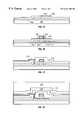
- FIGS. 1A through 1Dare diagrams showing steps of fabricating a pixel portion of an active matrix circuit
- FIGS. 2A and 2Bare diagrams showing steps of fabricating the pixel portion of the active matrix circuit
- FIGS. 3A and 3Bare diagram showing steps of fabricating the pixel portion of the active matrix circuit
- FIG. 4is a diagram showing a step of fabricating the pixel portion of the active matrix circuit
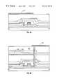
- FIGS. 5A through 5Fare diagrams showing steps of fabricating a thin film transistor constructed as a complementary type transistor.
- FIGS. 6A through 6Eare diagrams showing steps of fabricating a thin film transistor.
- FIGS. 1 and 2show steps of fabricating a pixel portion of an active matrix type liquid crystal display according to the present embodiment.
- silicon oxynitride filmit is also useful to use a silicon oxynitride film for the underlying layer. Because the silicon oxynitride film is dense and has a high adhesiveness with the glass substrate, it is highly functional as the underlying layer.
- the silicon oxynitride filmmay be formed by using mixed gas of silane, oxygen and N 2 O by means of plasma CVD. It may be obtained by using mixed gas of TEOS gas and N 2 O by means of plasma CVD.
- an amorphous silicon film not shownis formed. It becomes, later, a starting film of a thin film semiconductor which composes an active layer of the thin film transistor.
- the amorphous silicon film not showsis formed in a thickness of 500 ⁇ by using low pressure thermal CVD. It is noted that the plasma CVD may be used as a method for forming the amorphous silicon film.
- this amorphous silicon filmis crystallized by means of a heating process, irradiation of laser light or combination of the heating process and the irradiation of laser light.
- a crystalline silicon film not shownis obtained.
- this crystalline silicon film not shownis patterned to obtain an active layer 103 of the thin film transistor (FIG. 1 A).
- a silicon oxide film 104which covers the active layer 103 as shown in FIG. 1 A and functions as a gate insulating film is formed in a thickness of 1000 ⁇ by means of plasma CVD. Thus, a state shown in FIG. 1A is obtained.
- a silicon oxynitride filmas an insulating film which functions as the gate insulating film.
- an aluminum filmnot shown, containing 0.1 weight % of scandium is formed in a thickness of 4000 ⁇ by means of sputtering. This aluminum film composes a gate electrode later.
- a dense anodic oxide film not shownis formed on the surface thereof in a thickness of 100 ⁇ .
- This anodizationis carried out by using electrolyte in which ethylene glycol solution containing 3% of tartaric acid is neutralized by aqueous ammonia and by setting the aluminum film as an anode in the electrolyte.
- the thickness of the anodic oxide film to be formedmay be controlled by voltage attained.
- a resist mask not shownis placed to carry out patterning to form a gate electrode 105 .
- anodizationis carried out again while leaving the resist mask not shown. This anodization is carried out by using 3% aqueous oxalate as electrolyte.
- the anodic oxide film 106 having a porous natureis formed on the side of the gate electrode 105 .
- This porous anodic oxide filmmay be grown up to about several microns in thickness. This growth distance may be controlled by anodizing time.
- the anodic oxide film 106is formed in a thickness of 3000 ⁇ .
- anodizationis carried out again by using the electrolyte in which ethylene glycol solution containing 3% of tartaric acid is neutralized by aqueous ammonia. Because the electrolyte infiltrates into the inside of the porous anodic oxide film 106 in this anodization step, a dense anodic oxide film 107 is formed around the gate electrode 105 .
- a thickness of the dense anodic oxide film 107is 500 ⁇ .
- a main role of the dense anodic oxide film 107is to cover the surface of the gate electrode 105 so that no hillock nor whisker is grown in the later steps. It also has a role of protecting the gate electrode 105 so that the gate electrode 105 is not etched in removing the porous anodic oxide film 106 later. It also has a role of contributing in forming an offset gate region in a later step of injecting impurity ions. Thus, the state shown in FIG. 1B is obtained.
- Impurity ionsare injected in this state.
- P (phosphorus) ionsare injected in order to obtain an N-channel type thin film transistor.
- the impurity ionsare injected in the state in FIG. 1B, the impurity ions are injected selectively into regions 108 and 111 . In this step, the regions 108 and 111 become high concentration impurity regions.
- This region 110is an offset gate region which does not function as a source/drain region nor as a channel forming region.
- the size of this offset gate regionmay be decided according to the thickness of the dense anodic oxide film 107 and that of the porous anodic oxide film 106 .
- the offset gate regionrelaxes strength of an electric field formed between the channel forming region and the drain region in particular.
- the presence of the offset gate regionallows an OFF current value of the thin film transistor to be reduced and deterioration to be suppressed.
- the source region 108 , the channel forming region 109 , the offset gate region 110 and the drain region 111are formed in a self-aligned manner.
- a lightly doped regionmay be formed right below the porous anodic oxide film 106 .
- the drain side of this lightly doped regionis normally called as an LDD (lightly doped drain) region.
- the porous anodic oxide film 106is removed selectively.
- the porous anodic oxide film 106is removed selectively by using mixed acid of phosphoric acid, acetic acid and nitric acid.
- an annealing processis carried out by irradiating laser light. Because the laser light may by irradiated to the neighborhood of the interface between the high concentration impurity region and the offset gate region at this time, junction part which has been damaged by the injection of the impurity ions may be fully annealed.
- annealingmay be carried out by irradiating ultraviolet ray or infrared ray, instead of the laser light. It is useful to heat in conjunction with the irradiation of the laser light or intense light.
- a silicon oxide film 112is formed in a thickness of 2000 ⁇ as a first inter-layer insulating film.
- a silicon nitride film or a laminated film of a silicon oxide film and a silicon nitride filmmay be used.
- a contact holeis created through the first inter-layer insulating film 112 to create a source electrode 113 which contacts with the source region of the thin film transistor.
- This source electrode 113is formed as having a laminated structure of a titanium film, an aluminum film and titanium film.
- This source electrodeis also formed as what is extended from a source wire. That is, it is formed in the same time when source lines disposed in a matrix in an active matrix region are formed. Thus, the state shown in FIG. 1C is obtained.
- a silicon nitride film 114 having a thickness of 1000 ⁇is formed.
- This silicon nitride filmhas a function of suppressing fixed charge from existing in the interface with the thin film transistor by utilizing its dense film quality (generally the film quality of silicon nitride film is dense). It also has a function of preventing moisture and moving ions from infiltrating from the outside by utilizing its dense film quality.
- the silicon nitride film 114is formed by using silane and ammonium by means of plasma CVD.
- a silicon oxynitride filmmay be used beside the silicon nitride film.
- a silicon oxide film 115is formed in a thickness of 2000 ⁇ by means of plasma CVD. Although the silicon oxide film 115 is formed here in order to enhance its reliability, it may not be used specifically.
- an inter-layer insulating film 116is formed by using transparent polyimide resin or acrylic resin.
- the surface of the inter-layer insulating film 116 made from the resin materialis made to be flat.
- the thickness of the inter-layer insulating film 116 made from the resin materialis 2 ⁇ m.
- Capacity produced between the element and the electrodes and wires formed on the inter-layer insulating filmmay be reduced by creating the inter-layer insulating film by using the resin material. Further, it allows the production cost to be lowered considerably.
- the silicon oxide film 115is formed as the underlying layer below the inter-layer insulating film made from the resin material, adhesiveness with the underlying layers may be increased. Further, it allows a structure which suppresses moisture from infiltrating between the silicon oxide film 115 and the underlying layer to be created.
- This effectmay be obtained even when the inter-layer insulating film made from the resin material is formed on the silicon nitride film 114 , without forming the silicon oxide film 115 .
- a chrome film which functions as a light shielding film and as a black matrixis formed and is patterned to form a black matrix 117 functioning as the light shielding film as shown in FIG. 2 A.
- a resin material whose dielectric constant is less than 3may be selected for the resin material composing the inter-layer insulating film 116 . Its thickness may be increased to several ⁇ m. It is noted that because a time of fabrication step will not be prolonged even if the thickness of the resin material is thickened, it is useful to such an end.
- the problem of leakage of light caused by its irregularitymay be suppressed.
- a silicon nitride filmis formed further as an inter-layer insulating film 118 . Then, a silicon oxide film 119 is formed further.
- an inter-layer insulating film 120 made from a resin materialis formed.
- the materialmay be the same with that of the inter-layer insulating film 116 .
- inter-layer insulating film 120By forming the inter-layer insulating film 120 by the resin material, unnecessary capacity may be suppressed from being produced between a pixel electrode created later and the thin film transistor. Further, because its surface may be flattened, it becomes possible to suppress an electric field from the pixel electrode created later from being disturbed.
- an ITO electrode for forming the pixel electrodeis formed by means of sputtering and it is patterned to create the pixel electrode 121 .
- the structure shown in FIG. 2Bprevents unnecessary capacity from being produced because dielectric constant of the inter-layer insulating film disposed between the thin film transistor (specifically the source electrode 113 ) and the light shielding film (and/or black matrix) 117 may blowered and its thickness can be thickened.
- the present embodimentis characterized in that the structure illustrated in the first embodiment is improved further to increase the reliability.
- a metallic materialsuch as chrome is used for the light shielding film and black matrix
- an anodizable materialis used for the light shielding film for shielding the thin film transistor and an anodic oxide film is formed on the surface thereof in addition to the structure illustrated in the first embodiment.
- Aluminum or tantalummay be used as the anodizable material.
- a suitable light shielding filmmay be formed because the anodic oxide film may be colored in black or in color close to that by using the anodizing technology utilized in industrial products such as aluminum sash.
- FIGS. 3A and 3Bshow schematic fabrication steps of the present embodiment. It is noted that the same parts with those in FIG. 2 are not shown specifically in FIGS. 3A and 3B.
- FIG. 1Dthe state shown in FIG. 1D is obtained by following the steps shown in FIGS. 1A through 1D.
- a light shielding film 301is formed as shown in FIG. 3 A.
- the light shielding film 301is formed by using aluminum as its material.
- an anodic oxide film 302is formed on the surface of the light shielding film 301 as shown in FIG. 3A by carrying out anodization in electrolyte.
- the light shielding film 301is drawn as the light shielding film for shielding the thin film transistor in the figure, it is normally extended to form a black matrix.
- an inter-layer insulating film composed of a silicon nitride film and a silicon oxide film and an inter-layer insulating film composed of a resin materialare formed in a multi-layer.
- a pixel electrodeis formed by ITO, thus obtaining the state shown in FIG. 3 B.
- the structure shown in the present embodimentallows to suppress impurities from diffusing from the light shielding film 301 to the surroundings when the long-term reliability is concerned. Further, the light shielding film can be prevented from being short-circuited.
- the present embodimentrelates to a structure in which aperture ratio of a pixel is increased further.
- the present embodimentprovides a structure for reducing the problem of producing the capacity.
- FIG. 4shows the structure of the present embodiment.
- source lines and gate lines disposed in a matrixare caused to function as a black matrix and an area of the pixel electrode 402 is increased as much as possible.
- a light shielding film 401 for covering the main part of the thin film transistoris formed by a metallic material forming the source electrode (and the source line).
- Part of the source line and gate linemay be used as the black matrix by disposing the pixel electrode so that the part of the source line and gate line overlap the pixel electrode.
- the pixel electrodemay be disposed across the wide area when the structure shown in FIG. 4 is adopted, the aperture ratio of the pixel may be increased.
- the capacity produced between the pixel electrode 402 and the thin film transistormay be reduced because the inter-layer insulating film 116 made from the resin material exists.
- the silicon oxide film 115is formed across the whole surface below the resin material 116 forming the inter-layer insulating film and the silicon nitride film 114 is formed below that. Because the thin film transistor is covered by the silicon nitride film 114 , the electrical stability of the thin film transistor may be assured.
- the electrical stability of the thin film transistormay be enhanced because the silicon nitride film 114 can prevent moisture from diffusing from the inter-layer insulating film 116 made from the resin material to the thin film transistor section.
- the structure of the present embodimentmay be used for various thin film integrated circuits integrated on an insulating surface for example. It may be used also for a peripheral driving circuits of an active matrix type liquid crystal display for example.
- a silicon oxide film or a silicon oxynitride filmis formed as an underlying film 502 on a glass substrate 501 as shown in FIG. SA. Further, an amorphous silicon film not shown is formed further by means of plasma CVD or low pressure thermal CVD. This amorphous silicon film is transformed into crystalline silicon film by irradiating laser light or by applying heat to the amorphous silicon film.
- the crystalline silicon film thus obtainedis patterned to obtain active layers 503 and 504 .
- the state shown in FIG. 5Ais obtained.
- a silicon oxide film 505 which composes a gate insulating filmis formed. Then, an aluminum film not shown is formed in a thickness of 4000 ⁇ to form a gate electrode later. An anodizable metal (tantalum for example) may be used beside the aluminum film.
- a very thin and dense anodic oxide filmis formed on the surface thereof by the method described above.
- a resist mask not shownis disposed on the aluminum film to pattern the aluminum film. Then, anodization is carried out by using the aluminum pattern obtained as an anode to form porous anodic oxide films 508 and 509 .
- a thickness of the porous anodic oxide filmis 5000 ⁇ for example.
- Anodizationis carried out again under the condition of forming a dense anodic oxide film to form dense anodic oxide films 510 and 511 .
- a thickness of these dense anodic oxide films 510 and 511is 800 ⁇ .
- the exposed silicon oxide filmis removed by means of dry etching, thus obtaining the state shown in FIG. 5 C.
- the porous anodic oxide films 508 and 509are removed by using mixed acid of acetic acid, nitric acid and phosphoric acid.
- the state shown in FIG. 5Dis obtained.
- resist masksare disposed alternately so that, P ions are injected to the left thin film transistor and E ions are injected to the right thin film transistor.
- a high concentration N type source region 514 and drain region 517are formed in a self-aligned manner.
- a weak N type region in which the P ions are doped in low concentrationis formed in the same time. Further, a channel forming region 516 is formed in the same time.
- the weak N type region 515is formed because the remaining gate insulating film 512 exists. That is, the P ions which has transmitted through the gate insulating film 512 is partly blocked by the gate insulating film 512 .
- a strong P type source region 521 and drain region 518are formed in a self-aligned manner by the same principle.
- a low concentration impurity region 520 as well as a channel forming region 519are formed in the same time.
- an offset gate regioncan be formed by virtue of the thickness in contact with the channel forming region.
- the existence thereofmay be neglected in the case of the present embodiment because the thickness of the dense anodic oxide films 510 and 511 is so thin as less than 1000 ⁇ .
- the regions to which the impurity ions have been injectedare annealed by irradiating laser light or intense light.
- a silicon nitride film 522 and a silicon oxide film 523are formed as inter-layer insulating films as shown in FIG. 5 E. Their thickness is 1000 ⁇ . It is noted that the silicon oxide film 523 may not be formed.
- the thin film transistoris covered by the silicon nitride film.
- the reliability of the thin film transistormay be increased by adopting this structure because the silicon nitride film is dense and has a good interfacial characteristic.
- an inter-layer insulating film 524 made from a resin materialis formed by using spin coating.
- a thickness of the inter-layer insulating film 524is 1 82 m (FIG. 5 E).
- a source electrode 525 and a drain electrode 526 of the left N channel type thin film transistorare formed.
- a source electrode 527 and the drain electrode 526 of the right thin film transistorare formed.
- the drain electrode 526is disposed in common.
- CMOS structurehaving the complementarily constructed CMOS structure may be formed.
- the thin film transistoris covered by the nitride film and the resin material. This structure allows to form the device to which moving ions and moisture hardly infiltrate and which is highly durable.
- the present embodimentshows steps for fabricating a thin film transistor called a bottom gate type thin film transistor in which a gate electrode is located on the side of a substrate rather than an active layer.
- FIGS. 6A through 6Eshow the fabrication steps of the present embodiment.
- a silicon oxide film 602is formed as an underlying film on a glass substrate 601 by means of sputtering as shown in FIG. 6 A.
- a gate electrode 603is formed by aluminum.
- a silicon oxide film 604 which functions as a gate insulating filmis formed in a thickness of 500 ⁇ by means of plasma CVD.
- an amorphous silicon film(which becomes a crystalline silicon film 605 later) not shown which is a starting film for forming an active layer of the thin film transistor is formed by means of plasma CVD.
- Low pressure thermal CVDmay be used beside the plasma CVD.
- the amorphous silicon film not shownis crystallized by irradiating laser light.
- the crystalline silicon film 605is obtained.
- a silicon nitride film not shownis formed and exposure is carried out from the back of the substrate 601 by using the gate electrode 603 to form a mask pattern 607 made from a silicon nitride film.
- This mask pattern 607is formed as follows. At first, a resist mask pattern is formed by exposing from the back of the substrate 601 by utilizing the pattern of the gate electrode 603 . Further, ashing is carried out to cause this resist mask pattern to recede. Then, the pattern 607 is obtained by patterning the silicon nitride film by using the receded resist mask pattern (not shown).
- impuritiesare doped by using the mask pattern 607 .
- Pphosphorus
- plasma dopingis used as means for doping.
- Pis doped into regions 608 and 610 in this step. P is not doped into a region 609 .
- activation of the doped regions and annealing of damage caused by the impact of the dopant ionsare carried out by irradiating laser light from the top.
- the region 608is formed as a source region. Further, the region 610 is formed as a drain region. The region 609 is then defined as a channel region.
- an inter-layer insulating film 611 made from a silicon nitride filmis formed in a thickness of 2000 ⁇ by means of plasma CVD.
- the silicon nitride filmis most preferable as the inter-layer insulating film used here, because the silicon nitride film exhibits its effect most strongly in preventing an effect of moisture existing in a resin inter-layer film formed thereon later (effect to the active layer 606 ).
- a silicon oxide filmBeside the silicon nitride film, a silicon oxide film. a silicon oxynitride film or a laminated film of the silicon oxide film and the silicon nitride film (either of them may be put first in the order of lamination) may be used.
- a resin film 612 made from polyimideis formed as an inter-layer insulating film. It is formed by means of spin coating.
- contact holesare created to form a source electrode 613 and a drain electrode 614 .
- the utilization of the invention disclosed in the present specificationallows to obtain the structure of the semiconductor device which provides a high reliability, which can suppress the problem of capacity produced between the thin film transistor and the pixel electrode and wires and which provides low cost and highly productive semiconductor devices.
- the invention disclosed in the present specificationmay be utilized not only for the active matrix type liquid crystal display but also for EL type displays and IC circuits.
Landscapes
- Engineering & Computer Science (AREA)
- Physics & Mathematics (AREA)
- Microelectronics & Electronic Packaging (AREA)
- General Physics & Mathematics (AREA)
- Manufacturing & Machinery (AREA)
- Computer Hardware Design (AREA)
- Condensed Matter Physics & Semiconductors (AREA)
- Power Engineering (AREA)
- Nonlinear Science (AREA)
- Mathematical Physics (AREA)
- Chemical & Material Sciences (AREA)
- Crystallography & Structural Chemistry (AREA)
- Optics & Photonics (AREA)
- Thin Film Transistor (AREA)
Abstract
Description
This is a continuation of U.S. application Ser. No. 08/767,179, filed Dec. 16, 1996, now U.S. Pat. No. 5,990,542.
1. Field of the Invention
The present invention relates to a structure of a semiconductor device which can be used for a flat panel display typified by an active matrix type liquid crystal display and an EL type display unit and more particularly to a structure of an inter-layer insulating film of a semiconductor device typified by a thin film transistor.
2. Description of Related Art
Hitherto, an active matrix type liquid crystal display has been known as a typical flat panel display. It has a structure in which a switching thin film transistor is provided in each of a large number of pixels disposed in a matrix and charge input/output to/from each pixel electrode is controlled by this thin film transistor.
In such a structure, it is necessary to coat the semiconductor device by an insulating film to prevent moisture, impurities and moving ions (e.g. sodium ions) which are great enemy of the semiconductor device from infiltrating. Further, it must be constructed such that capacity produced between the pixel electrode, wires and the thin film transistor can be reduced.
Further, it is required to have a low production cost and an excellent productivity. However, it is the present situation that those requirements cannot be met with a silicon oxide film or a silicon nitride film which are normally utilized as an inter-layer insulating film.
Accordingly, it is an object of the present invention disclosed in this specification to provide a novel structure required to the aforementioned inter-layer insulating film. That is, it is an object of the present invention to provide a structure of a semiconductor device having an inter-layer insulating film which can prevent moisture and impurities from infiltrating, which can suppress the capacity produces between the thin film transistor, pixel electrode and wires, whose cost is low and which has a high productivity.
According to one of the present invention disclosed in the present specification, a semiconductor device comprises an inter-layer insulating film made from a resin material disposed at the upper part of a semiconductor element; and a silicon oxide film or a silicon nitride film formed on, the whole surface of an underlying layer on which the interlayer insulating film is formed.
According to another structure of the present invention, a semiconductor device comprises an inter-layer insulating film made from a resin material disposed at the upper part of a semiconductor element; and a laminated film of a silicon oxide film and a silicon nitride film formed on the whole surface of an underlying layer on which the inter-layer insulating film is formed.
In the above-mentioned structure, either the silicon oxide film or the silicon nitride film may be put first in the order of lamination. However, it is preferable to form the silicon nitride film as the lower layer from its adhesiveness and good interfacial characteristics when the semiconductor element is to be covered.
According to a still other structure of the present invention, a semiconductor device comprises an inter-layer insulating film made from a resin material disposed at the upper part of a semiconductor element; and a silicon oxynitride film formed on the whole surface of an underlying layer on which the inter-layer insulating film is formed.
According to another structure of the present invention, a semiconductor device comprises an inter-layer insulating film made from a resin material disposed at the upper part of a semiconductor element; and a silicon oxide film or a silicon nitride film formed between the semiconductor element and the inter-layer insulating film.
According to a still other structure of the present invention, a semiconductor device comprises an inter-layer insulating film made from a resin material disposed at the upper part of a semiconductor element; and a silicon oxynitride film formed between the semiconductor element and the inter-layer insulating film.
According to a still other structure of the present invention, a semiconductor device comprises an inter-layer insulating film made from a resin material disposed at the upper part of a semiconductor element; and a laminated film of a silicon oxide film and a silicon nitride film formed between the semiconductor element and the inter-layer insulating film.
Capacity produced between a pixel electrode, wires and a thin film transistor may be reduced by using the laminated film of the silicon nitride film and the resin film as the inter-layer insulating film covering the upper part of the thin film transistor.
Further, because it is possible to flatten the surface of the resin material, no section for riding across a difference in level of wires is formed, thus allowing to prevent local change of resistance of the wires and breaking of the wires.
Further, it is possible to suppress moisture within the resin film from exerting an ill effect to the operation of the thin film transistor by providing the silicon nitride film between the resin film and the thin film transistor so that the resin film does not contact directly with the thin film transistor.
The above and other related objects and features of the invention will be apparent from a reading of the following description of the disclosure found in the accompanying drawings and the novelty thereof pointed out in the appended claims.
FIGS. 1A through 1D are diagrams showing steps of fabricating a pixel portion of an active matrix circuit;
FIGS. 2A and 2B are diagrams showing steps of fabricating the pixel portion of the active matrix circuit;
FIGS. 3A and 3B are diagram showing steps of fabricating the pixel portion of the active matrix circuit;
FIG. 4 is a diagram showing a step of fabricating the pixel portion of the active matrix circuit;
FIGS. 5A through 5F are diagrams showing steps of fabricating a thin film transistor constructed as a complementary type transistor; and
FIGS. 6A through 6E are diagrams showing steps of fabricating a thin film transistor.
[First Embodiment]
FIGS. 1 and 2 show steps of fabricating a pixel portion of an active matrix type liquid crystal display according to the present embodiment.
At first, asilicon oxide film 102 is formed in a thickness of 3000 Å on aglass substrate 101 as an underlying layer by means of plasma CVD as shown in FIG.1A. This underlying layer has a function of suppressing impurities from diffusing from the glass substrate to a semiconductor layer formed later. It also has a function of relaxing stress which acts between the glass substrate and the semiconductor layer formed later.
It is also useful to use a silicon oxynitride film for the underlying layer. Because the silicon oxynitride film is dense and has a high adhesiveness with the glass substrate, it is highly functional as the underlying layer.
The silicon oxynitride film may be formed by using mixed gas of silane, oxygen and N2O by means of plasma CVD. It may be obtained by using mixed gas of TEOS gas and N2O by means of plasma CVD.
Next, an amorphous silicon film not shown is formed. It becomes, later, a starting film of a thin film semiconductor which composes an active layer of the thin film transistor. Here, the amorphous silicon film not shows is formed in a thickness of 500 Å by using low pressure thermal CVD. It is noted that the plasma CVD may be used as a method for forming the amorphous silicon film.
Then, this amorphous silicon film is crystallized by means of a heating process, irradiation of laser light or combination of the heating process and the irradiation of laser light. Thus, a crystalline silicon film not shown is obtained.
Then, this crystalline silicon film not shown is patterned to obtain anactive layer 103 of the thin film transistor (FIG.1A).
Next, asilicon oxide film 104 which covers theactive layer 103 as shown in FIG.1A and functions as a gate insulating film is formed in a thickness of 1000 Å by means of plasma CVD. Thus, a state shown in FIG. 1A is obtained.
It is preferable to use a silicon oxynitride film as an insulating film which functions as the gate insulating film.
Next, an aluminum film, not shown, containing 0.1 weight % of scandium is formed in a thickness of 4000 Å by means of sputtering. This aluminum film composes a gate electrode later.
After forming the aluminum film, a dense anodic oxide film not shown is formed on the surface thereof in a thickness of 100 Å. This anodization is carried out by using electrolyte in which ethylene glycol solution containing 3% of tartaric acid is neutralized by aqueous ammonia and by setting the aluminum film as an anode in the electrolyte.
In this anodization, the thickness of the anodic oxide film to be formed may be controlled by voltage attained.
Further, a resist mask not shown is placed to carry out patterning to form agate electrode 105.
After forming thegate electrode 105, anodization is carried out again while leaving the resist mask not shown. This anodization is carried out by using 3% aqueous oxalate as electrolyte.
In this anodization, only the side of thegate electrode 105 is anodized selectively because the resist mask not shown remains. An anodic oxide film having a porous structure may be obtained in this step.
Thus, theanodic oxide film 106 having a porous nature is formed on the side of thegate electrode 105.
This porous anodic oxide film may be grown up to about several microns in thickness. This growth distance may be controlled by anodizing time. Here, theanodic oxide film 106 is formed in a thickness of 3000 Å.
Next, anodization is carried out again by using the electrolyte in which ethylene glycol solution containing 3% of tartaric acid is neutralized by aqueous ammonia. Because the electrolyte infiltrates into the inside of the porousanodic oxide film 106 in this anodization step, a denseanodic oxide film 107 is formed around thegate electrode 105.
A thickness of the denseanodic oxide film 107 is 500 Å. A main role of the denseanodic oxide film 107 is to cover the surface of thegate electrode 105 so that no hillock nor whisker is grown in the later steps. It also has a role of protecting thegate electrode 105 so that thegate electrode 105 is not etched in removing the porousanodic oxide film 106 later. It also has a role of contributing in forming an offset gate region in a later step of injecting impurity ions. Thus, the state shown in FIG. 1B is obtained.
Impurity ions are injected in this state. Here, P (phosphorus) ions are injected in order to obtain an N-channel type thin film transistor.
When the impurity ions are injected in the state in FIG. 1B, the impurity ions are injected selectively intoregions regions
No impurity ions are injected to aregion 109 right under thegate electrode 105 because thegate electrode 105 becomes a mask thereof. Thisregion 109 becomes a channel forming region.
Further, no impurity ions are injected also into aregion 110 because the porousanodic oxide film 106 and the denseanodic oxide film 107 become masks thereof. Thisregion 110 is an offset gate region which does not function as a source/drain region nor as a channel forming region. The size of this offset gate region may be decided according to the thickness of the denseanodic oxide film 107 and that of the porousanodic oxide film 106.
The offset gate region relaxes strength of an electric field formed between the channel forming region and the drain region in particular. The presence of the offset gate region allows an OFF current value of the thin film transistor to be reduced and deterioration to be suppressed.
Thus, thesource region 108, thechannel forming region 109, the offsetgate region 110 and thedrain region 111 are formed in a self-aligned manner.
It is noted that there is a method of removing the porous anodic oxide film after injecting the impurity ions and of injecting impurity ions again under a light doping condition. In this case, a lightly doped region may be formed right below the porousanodic oxide film 106. The drain side of this lightly doped region is normally called as an LDD (lightly doped drain) region.
After injecting the impurity ions, the porousanodic oxide film 106 is removed selectively. Here, the porousanodic oxide film 106 is removed selectively by using mixed acid of phosphoric acid, acetic acid and nitric acid.
Then, an annealing process is carried out by irradiating laser light. Because the laser light may by irradiated to the neighborhood of the interface between the high concentration impurity region and the offset gate region at this time, junction part which has been damaged by the injection of the impurity ions may be fully annealed.
It is noted that the above-mentioned annealing may be carried out by irradiating ultraviolet ray or infrared ray, instead of the laser light. It is useful to heat in conjunction with the irradiation of the laser light or intense light.
After obtaining the state shown in FIG. 1B, asilicon oxide film 112 is formed in a thickness of 2000 Å as a first inter-layer insulating film. For the first inter-layer insulating film, a silicon nitride film or a laminated film of a silicon oxide film and a silicon nitride film may be used.
Next, a contact hole is created through the firstinter-layer insulating film 112 to create asource electrode 113 which contacts with the source region of the thin film transistor. This source electrode113 is formed as having a laminated structure of a titanium film, an aluminum film and titanium film. This source electrode is also formed as what is extended from a source wire. That is, it is formed in the same time when source lines disposed in a matrix in an active matrix region are formed. Thus, the state shown in FIG. 1C is obtained.
Next, asilicon nitride film 114 having a thickness of 1000 Å is formed. This silicon nitride film has a function of suppressing fixed charge from existing in the interface with the thin film transistor by utilizing its dense film quality (generally the film quality of silicon nitride film is dense). It also has a function of preventing moisture and moving ions from infiltrating from the outside by utilizing its dense film quality.
Thesilicon nitride film 114 is formed by using silane and ammonium by means of plasma CVD. A silicon oxynitride film may be used beside the silicon nitride film.
Next, asilicon oxide film 115 is formed in a thickness of 2000 Å by means of plasma CVD. Although thesilicon oxide film 115 is formed here in order to enhance its reliability, it may not be used specifically.
Further, an inter-layerinsulating film 116 is formed by using transparent polyimide resin or acrylic resin. The surface of the inter-layerinsulating film 116 made from the resin material is made to be flat. The thickness of the inter-layerinsulating film 116 made from the resin material is 2 μm. Thus, the state shown in FIG. 1D is obtained.
Capacity produced between the element and the electrodes and wires formed on the inter-layer insulating film may be reduced by creating the inter-layer insulating film by using the resin material. Further, it allows the production cost to be lowered considerably.
Because thesilicon oxide film 115 is formed as the underlying layer below the inter-layer insulating film made from the resin material, adhesiveness with the underlying layers may be increased. Further, it allows a structure which suppresses moisture from infiltrating between thesilicon oxide film 115 and the underlying layer to be created.
This effect may be obtained even when the inter-layer insulating film made from the resin material is formed on thesilicon nitride film 114, without forming thesilicon oxide film 115.
Next, a chrome film which functions as a light shielding film and as a black matrix is formed and is patterned to form ablack matrix 117 functioning as the light shielding film as shown in FIG.2A.
Here, a resin material whose dielectric constant is less than 3 may be selected for the resin material composing the inter-layerinsulating film 116. Its thickness may be increased to several μm. It is noted that because a time of fabrication step will not be prolonged even if the thickness of the resin material is thickened, it is useful to such an end.
By constructing as described above, it is possible to suppress capacity from being produced between thelight shielding film 117 made from chrome and the underlying thin film transistor.
Further, because it is easy to flatten the surface of the inter-layerinsulating film 116 when it is made form the resin material, the problem of leakage of light caused by its irregularity may be suppressed.
After obtaining the state shown in FIG. 2A, a silicon nitride film is formed further as an inter-layerinsulating film 118. Then, asilicon oxide film 119 is formed further.
Although a two-layered structure of the silicon nitride film and the silicon oxide film has been adopted here in order to increase the reliability, a single layer structure of either of them may be adopted.
Further, an inter-layerinsulating film 120 made from a resin material is formed. The material may be the same with that of the inter-layerinsulating film 116.
By forming the inter-layerinsulating film 120 by the resin material, unnecessary capacity may be suppressed from being produced between a pixel electrode created later and the thin film transistor. Further, because its surface may be flattened, it becomes possible to suppress an electric field from the pixel electrode created later from being disturbed.
Then, a contact hole is created, an ITO electrode for forming the pixel electrode is formed by means of sputtering and it is patterned to create thepixel electrode 121.
Thus, the structure shown in FIG. 2B is completed. The structure shown in FIG. 2B prevents unnecessary capacity from being produced because dielectric constant of the inter-layer insulating film disposed between the thin film transistor (specifically the source electrode113) and the light shielding film (and/or black matrix)117 may blowered and its thickness can be thickened.
Because it is easy, industrially, to thicken the resin film and it will not increase a processing time as described above, the above-mentioned structure may be readily realized.
[Second Embodiment]
The present embodiment is characterized in that the structure illustrated in the first embodiment is improved further to increase the reliability.
As described above, a metallic material such as chrome is used for the light shielding film and black matrix However, when a long-term reliability is concerned, there may be problems of diffusion of impurities from the metallic material and of short-circuit caused between the metallic material and other electrodes and wires.
Then, in a structure illustrated in the present embodiment, an anodizable material is used for the light shielding film for shielding the thin film transistor and an anodic oxide film is formed on the surface thereof in addition to the structure illustrated in the first embodiment.
Aluminum or tantalum may be used as the anodizable material. When aluminum is used in particular, a suitable light shielding film may be formed because the anodic oxide film may be colored in black or in color close to that by using the anodizing technology utilized in industrial products such as aluminum sash.
FIGS. 3A and 3B show schematic fabrication steps of the present embodiment. It is noted that the same parts with those in FIG. 2 are not shown specifically in FIGS. 3A and 3B.
At first, the state shown in FIG. 1D is obtained by following the steps shown in FIGS. 1A through 1D. Next, alight shielding film 301 is formed as shown in FIG.3A. Here, thelight shielding film 301 is formed by using aluminum as its material.
Then, ananodic oxide film 302 is formed on the surface of thelight shielding film 301 as shown in FIG. 3A by carrying out anodization in electrolyte.
Although thelight shielding film 301 is drawn as the light shielding film for shielding the thin film transistor in the figure, it is normally extended to form a black matrix.
After obtaining the state shown in FIG. 3A, an inter-layer insulating film composed of a silicon nitride film and a silicon oxide film and an inter-layer insulating film composed of a resin material are formed in a multi-layer.
Further, a pixel electrode is formed by ITO, thus obtaining the state shown in FIG.3B.
Because theanodic oxide film 302 is chemically stable, the structure shown in the present embodiment allows to suppress impurities from diffusing from thelight shielding film 301 to the surroundings when the long-term reliability is concerned. Further, the light shielding film can be prevented from being short-circuited.
[Third Embodiment]
The present embodiment relates to a structure in which aperture ratio of a pixel is increased further. Generally, it is desired to increase the aperture ratio of the pixel as much as possible. It is necessary to dispose the pixel electrode in a widest possible area in order to increase the aperture ratio of the pixel.
However, because capacity is produced between the pixel electrode and the thin film transistor and the wires when they are overlapped each other, it has been limited greatly in this aspect in general.
The present embodiment provides a structure for reducing the problem of producing the capacity.
FIG. 4 shows the structure of the present embodiment. In the structure shown in FIG. 4, source lines and gate lines disposed in a matrix are caused to function as a black matrix and an area of thepixel electrode 402 is increased as much as possible.
In the structure shown in FIG. 4, alight shielding film 401 for covering the main part of the thin film transistor is formed by a metallic material forming the source electrode (and the source line).
Part of the source line and gate line may be used as the black matrix by disposing the pixel electrode so that the part of the source line and gate line overlap the pixel electrode.
Because the pixel electrode may be disposed across the wide area when the structure shown in FIG. 4 is adopted, the aperture ratio of the pixel may be increased.
Further, even if such structure is adopted, the capacity produced between thepixel electrode 402 and the thin film transistor may be reduced because the inter-layerinsulating film 116 made from the resin material exists.
Still more, it can be alleviated that unnecessary pressure would be applied to the thin film transistor in a rubbing step and panel assembling step after forming thepixel electrode 402, by using the resin material as the inter-layer insulating film.
Thesilicon oxide film 115 is formed across the whole surface below theresin material 116 forming the inter-layer insulating film and thesilicon nitride film 114 is formed below that. Because the thin film transistor is covered by thesilicon nitride film 114, the electrical stability of the thin film transistor may be assured.
The electrical stability of the thin film transistor may be enhanced because thesilicon nitride film 114 can prevent moisture from diffusing from the inter-layerinsulating film 116 made from the resin material to the thin film transistor section.
[Fourth Embodiment]
A case when an N-channel type thin film transistor and a P-channel type thin film transistor are formed complementarily is shown in the present embodiment. The structure of the present embodiment may be used for various thin film integrated circuits integrated on an insulating surface for example. It may be used also for a peripheral driving circuits of an active matrix type liquid crystal display for example.
At first, a silicon oxide film or a silicon oxynitride film is formed as anunderlying film 502 on aglass substrate 501 as shown in FIG. SA. Further, an amorphous silicon film not shown is formed further by means of plasma CVD or low pressure thermal CVD. This amorphous silicon film is transformed into crystalline silicon film by irradiating laser light or by applying heat to the amorphous silicon film.
The crystalline silicon film thus obtained is patterned to obtainactive layers
Further, asilicon oxide film 505 which composes a gate insulating film is formed. Then, an aluminum film not shown is formed in a thickness of 4000 Å to form a gate electrode later. An anodizable metal (tantalum for example) may be used beside the aluminum film.
After forming the aluminum film, a very thin and dense anodic oxide film is formed on the surface thereof by the method described above.
Next, a resist mask not shown is disposed on the aluminum film to pattern the aluminum film. Then, anodization is carried out by using the aluminum pattern obtained as an anode to form porousanodic oxide films
Anodization is carried out again under the condition of forming a dense anodic oxide film to form denseanodic oxide films anodic oxide films
Then, the exposed silicon oxide film is removed by means of dry etching, thus obtaining the state shown in FIG.5C.
After obtaining the state shown in FIG. 5C, the porousanodic oxide films
Here, resist masks are disposed alternately so that, P ions are injected to the left thin film transistor and E ions are injected to the right thin film transistor.
By injecting the impurity ions, a high concentration Ntype source region 514 and drainregion 517 are formed in a self-aligned manner.
Further, a weak N type region in which the P ions are doped in low concentration is formed in the same time. Further, achannel forming region 516 is formed in the same time.
The weakN type region 515 is formed because the remaininggate insulating film 512 exists. That is, the P ions which has transmitted through thegate insulating film 512 is partly blocked by thegate insulating film 512.
A strong Ptype source region 521 and drainregion 518 are formed in a self-aligned manner by the same principle. A lowconcentration impurity region 520 as well as achannel forming region 519 are formed in the same time.
When the denseanodic oxide films
The existence thereof may be neglected in the case of the present embodiment because the thickness of the denseanodic oxide films
Then, the regions to which the impurity ions have been injected are annealed by irradiating laser light or intense light.
Then, asilicon nitride film 522 and asilicon oxide film 523 are formed as inter-layer insulating films as shown in FIG.5E. Their thickness is 1000 Å. It is noted that thesilicon oxide film 523 may not be formed.
Here, the thin film transistor is covered by the silicon nitride film. The reliability of the thin film transistor may be increased by adopting this structure because the silicon nitride film is dense and has a good interfacial characteristic.
Further, an inter-layerinsulating film 524 made from a resin material is formed by using spin coating. Here, a thickness of the inter-layerinsulating film 524 is 182 m (FIG.5E).
Then, contact holes are created and asource electrode 525 and adrain electrode 526 of the left N channel type thin film transistor are formed. In the same time, asource electrode 527 and thedrain electrode 526 of the right thin film transistor are formed. Here, thedrain electrode 526 is disposed in common.
Thus, a thin film transistor circuit having the complementarily constructed CMOS structure may be formed.
In the structure shown in the present embodiment, the thin film transistor is covered by the nitride film and the resin material. This structure allows to form the device to which moving ions and moisture hardly infiltrate and which is highly durable.
Further, it allows to prevent capacity from being produced between the thin film transistor and wires when multi-layered wires is formed.
[Fifth Embodiment]
The present embodiment shows steps for fabricating a thin film transistor called a bottom gate type thin film transistor in which a gate electrode is located on the side of a substrate rather than an active layer.
FIGS. 6A through 6E show the fabrication steps of the present embodiment. At first, asilicon oxide film 602 is formed as an underlying film on aglass substrate 601 by means of sputtering as shown in FIG.6A. Next, agate electrode 603 is formed by aluminum.
At this time, 0.18 weight % of scandium is contained in the aluminum. Further, other impurities are reduced as much as possible to lower their concentration. These are carried out in order to suppress projections called hillock or whisker from being formed by abnormal growth of the aluminum in the later steps.
Thus, the state shown in FIG. 6A is obtained. Next, asilicon oxide film 604 which functions as a gate insulating film is formed in a thickness of 500 Å by means of plasma CVD.
Further, an amorphous silicon film (which becomes acrystalline silicon film 605 later) not shown which is a starting film for forming an active layer of the thin film transistor is formed by means of plasma CVD. Low pressure thermal CVD may be used beside the plasma CVD.
Next, the amorphous silicon film not shown is crystallized by irradiating laser light. Thus, thecrystalline silicon film 605 is obtained.
Thus, the state shown in FIG. 6B is obtained. After obtaining the state shown in FIG. 6B, patterning is carried out to obtain anactive layer 606.
Next, a silicon nitride film not shown is formed and exposure is carried out from the back of thesubstrate 601 by using thegate electrode 603 to form amask pattern 607 made from a silicon nitride film.
Thismask pattern 607 is formed as follows. At first, a resist mask pattern is formed by exposing from the back of thesubstrate 601 by utilizing the pattern of thegate electrode 603. Further, ashing is carried out to cause this resist mask pattern to recede. Then, thepattern 607 is obtained by patterning the silicon nitride film by using the receded resist mask pattern (not shown).
Thus, the state shown in FIG. 6C is obtained. Next, impurities are doped by using themask pattern 607. Here, P (phosphorus) is used as a dopant and plasma doping is used as means for doping.
P is doped intoregions region 609.
After finishing the doping, activation of the doped regions and annealing of damage caused by the impact of the dopant ions are carried out by irradiating laser light from the top.
Thus, theregion 608 is formed as a source region. Further, theregion 610 is formed as a drain region. Theregion 609 is then defined as a channel region.
Thus, the state shown in FIG. 6D is obtained. Next, an inter-layerinsulating film 611 made from a silicon nitride film is formed in a thickness of 2000 Å by means of plasma CVD.
The silicon nitride film is most preferable as the inter-layer insulating film used here, because the silicon nitride film exhibits its effect most strongly in preventing an effect of moisture existing in a resin inter-layer film formed thereon later (effect to the active layer606).
Beside the silicon nitride film, a silicon oxide film. a silicon oxynitride film or a laminated film of the silicon oxide film and the silicon nitride film (either of them may be put first in the order of lamination) may be used.
Next, aresin film 612 made from polyimide is formed as an inter-layer insulating film. It is formed by means of spin coating.
Further, contact holes are created to form asource electrode 613 and adrain electrode 614.
There has been a problem when the resin material is used as the inter-layer insulating film that the characteristic of the device is influenced by the moisture (OH radical in particular) existing in the resin material. However, such problem which arises when the resin material is used for the inter-layer insulating film may be suppressed by providing the silicon nitride film which prevents moisture from moving as described in the present embodiment.
The utilization of the invention disclosed in the present specification allows to obtain the structure of the semiconductor device which provides a high reliability, which can suppress the problem of capacity produced between the thin film transistor and the pixel electrode and wires and which provides low cost and highly productive semiconductor devices. The invention disclosed in the present specification may be utilized not only for the active matrix type liquid crystal display but also for EL type displays and IC circuits.
While preferred embodiments have been described, variations thereto will occur to those skilled in the art within the scope of the present inventive concepts which are delineated by the following claims.
Claims (60)
1. An EL type display comprising:
a substrate;
a thin film transistor formed over said substrate, said thin film transistor comprising a semiconductor film having a channel region and a gate electrode adjacent to said channel forming region with a gate insulating film therebetween;
a first organic film comprising a resin material formed over at least said semiconductor film and said gate electrode;
an insulating film formed on said first organic film;
a second organic film comprising a resin material formed on said insulating film; and
a pixel electrode formed over said second organic film.
2. An EL type display according toclaim 1 , wherein said resin material of said first organic film comprises at least one material selected from the group consisting of polyimide and acrylic.
3. An EL type display according toclaim 1 , wherein said resin material of said second organic film comprises at least one material selected from the group consisting of polyimide and acrylic.
4. An EL type display comprising:
a substrate;
a thin film transistor formed over said substrate, said thin film transistor comprising a semiconductor film having a channel forming region and a gate electrode adjacent to said channel forming region with a gate insulating film therebetween;
a first organic film comprising a resin material formed over at least said semiconductor film and said gate electrode;
an insulating film comprising silicon oxide formed on said first organic film;
a second organic film comprising a resin material formed on said insulating film; and
a pixel electrode formed over said second organic film.
5. An EL type display according toclaim 4 , wherein said resin material of said first organic film comprises at least one material selected from the group consisting of polyimide and acrylic.
6. An EL type display according toclaim 4 , wherein said resin material of said second organic film comprises at least one material selected from the group consisting of polyimide and acrylic.
7. An EL type display according toclaim 4 , further comprising a second insulating film interposed between said first organic resin film and said semiconductor film, wherein said second insulating film comprises at least one material selected from the group consisting of silicon oxide, silicon nitride, and silicon oxynitride.
8. An EL type display comprising:
a substrate;
a thin film transistor formed over said substrate, said thin film transistor comprising a semiconductor film having a channel forming region and a gate electrode adjacent to said channel forming region with a gate insulating film therebetween;
a first organic film comprising a resin material formed over at least said semiconductor film and said gate electrode;
an insulating film comprising silicon nitride formed on said first organic film;
a second organic film comprising a resin material formed on said insulating film; and
a pixel electrode formed over said second organic film.
9. An EL type display according toclaim 8 , wherein said resin material of said first organic film comprises at least one material selected from the group consisting of polyimide and acrylic.
10. An EL type display according toclaim 8 , wherein said resin material of said second organic film comprises at least one material selected from the group consisting of polyimide and acrylic.
11. An EL type display according toclaim 8 , further comprising a second insulating film interposed between said first organic resin film and said semiconductor film, wherein said second insulating film comprises at least one material selected from the group consisting of silicon oxide, silicon nitride, and silicon oxynitride.
12. An EL type display comprising:
a substrate;
a thin film transistor formed over said substrate, said thin film transistor comprising a semiconductor film having a channel forming region and a gate electrode adjacent to said channel forming region with a gate insulating film therebetween;
a first organic film comprising a resin material formed over at least said semiconductor film and said gate electrode;
an insulating film having a laminate structure of at least two films formed on said first organic film;
a second organic film comprising a resin material formed on said insulating film; and
a pixel electrode formed over said second organic film.
13. An EL type display according toclaim 12 , wherein said resin material of said first organic film comprises at least one material selected from the group consisting of polyimide and acrylic.
14. An EL type display according toclaim 12 , wherein said resin material of said second organic film comprises at least one material selected from the group consisting of polyimide and acrylic.
15. An EL type display according toclaim 12 , wherein said insulating film comprises at least one material selected from the group consisting of silicon oxide and silicon nitride.
16. An EL type display comprising:
a substrate;
a thin film transistor formed over said substrate, said thin film transistor comprising a semiconductor film having a channel forming region and a gate electrode adjacent to said channel forming region with a gate insulating film therebetween;
a first insulating film formed over at least said semiconductor film and said gate electrode;
a first organic film comprising a resin material formed on said first insulating film;
a second insulating film formed on said first organic film;
a second organic film comprising a resin material formed on said insulating film; and
a pixel electrode formed over said second organic film.
17. An EL type display according toclaim 16 , wherein said resin material of said first organic film comprises at least one material selected from the group consisting of polyimide and acrylic.
18. An EL type display according toclaim 16 , wherein said resin material of said second organic film comprises at least one material selected from the group consisting of polyimide and acrylic.
19. An EL type display according toclaim 16 , wherein said first insulating film comprises at least one material selected from the group consisting of silicon oxide, silicon nitride, and silicon oxynitride.
20. An EL type display comprising:
a substrate;
a thin film transistor formed over said substrate, said thin film transistor comprising a semiconductor film having a channel forming region and a gate electrode adjacent to said channel forming region with a gate insulating film therebetween;
a first insulating film formed over at least said semiconductor film and said gate electrode;
a first organic film comprising a resin material formed on said first insulating film;
a second insulating film having a laminate structure of at least two films formed on said first organic film;
a second organic film comprising a resin material formed on said insulating film; and
a pixel electrode formed over said second organic film.
21. An EL type display according toclaim 20 , wherein said resin material of said first organic film comprises at least one material selected from the group consisting of polyimide and acrylic.
22. An EL type display according toclaim 20 , wherein said resin material of said second organic film comprises at least one material selected from the group consisting of polyimide and acrylic.
23. An EL type display according toclaim 20 , wherein said first insulating film comprises at least one material selected from the group consisting of silicon oxide, silicon nitride, and silicon oxynitride.
24. An EL type display according toclaim 20 , wherein said second insulating film comprises at least one material selected from the group consisting of silicon oxide and silicon nitride.
25. An EL type display comprising:
a substrate;
a first organic film comprising a resin material formed over said substrate;
an insulating film formed on said first organic film;
a second organic film comprising a resin material formed on said insulating film; and
an electrode formed over said second organic film.
26. An EL type display according toclaim 25 , wherein said resin material of said first organic film comprises at least one material selected from the group consisting of polyimide and acrylic.
27. An EL type display according toclaim 25 , wherein said resin material of said second organic film comprises at least one material selected from the group consisting of polyimide and acrylic.
28. An EL type display according toclaim 25 , wherein said electrode is formed on said second organic film.
29. An EL type display according toclaim 25 , wherein said electrode comprises an indium tin oxide.
30. An EL type display comprising:
a substrate;
a first organic film comprising a resin material formed over said substrate;
an insulating film comprising silicon oxide formed on said first organic film;
a second organic film comprising a resin material formed on said insulating film; and
an electrode formed over said second organic film.
31. An EL type display according toclaim 30 , wherein said resin material of said first organic film comprises at least one material selected from the group consisting of polyimide and acrylic.
32. An EL type display according toclaim 30 , wherein said resin material of said second organic film comprises at least one material selected from the group consisting of polyimide and acrylic.
33. An EL type display according toclaim 30 , wherein said electrode is formed on said second organic film.
34. An EL type display according toclaim 30 , wherein said electrode comprises an indium tin oxide.
35. An EL type display according toclaim 30 , further comprising a second insulating film interposed between said first organic resin film and said substrate, wherein said second insulating film comprises at least one material selected from the group consisting of silicon oxide, silicon nitride, and silicon oxynitride.
36. An EL type display comprising:
a substrate;
a first organic film comprising a resin material formed over said substrate;
an insulating film comprising silicon nitride formed on said first organic film;
a second organic film comprising a resin material formed on said insulating film; and
an electrode formed over said second organic film.
37. An EL type display according toclaim 36 , wherein said resin material of said first organic film comprises at least one material selected from the group consisting of polyimide and acrylic.
38. An EL type display according toclaim 36 , wherein said resin material of said second organic film comprises at least one material selected from the group consisting of polyimide and acrylic.
39. An EL type display according toclaim 36 , wherein said electrode is formed on said second organic film.
40. An EL type display according toclaim 36 , wherein said electrode comprises an indium tin oxide.
41. An EL type display according toclaim 36 , further comprising a second insulating film interposed between said first organic resin film and said substrate, wherein said second insulating film comprises at least one material selected from the group consisting of silicon oxide, silicon nitride, and silicon oxynitride.
42. An EL type display comprising:
a substrate;
a first organic film comprising a resin material formed over said substrate;
an insulating film having a laminate structure of at least two films formed on said first organic film;
a second organic film comprising a resin material formed on said insulating film, and
an electrode formed over said second organic film.
43. An EL type display according toclaim 42 , wherein said resin material of said first organic film comprises at least one material selected from the group consisting of polyimide and acrylic.
44. An EL type display according toclaim 42 , wherein said resin material of said second organic film comprises at least one material selected from the group consisting of polyimide and acrylic.
45. An EL type display according toclaim 42 , wherein said insulating film comprises at least one material selected from the group consisting of silicon oxide and silicon nitride.
46. An EL type display according toclaim 42 , wherein said electrode is formed on said second organic film.
47. An EL type display according toclaim 42 , wherein said electrode comprises an indium tin oxide.
48. An EL type display comprising:
a substrate;
a first insulating film formed over said substrate;
a first organic film comprising a resin material formed on said first insulating film;
a second insulating film formed on said first organic film;
a second organic film comprising a resin material formed on said insulating film; and
an electrode formed over said second organic film.
49. An EL type display according toclaim 48 , wherein said resin material of said first organic film comprises at least one material selected from the group consisting of polyimide and acrylic.
50. An EL type display according toclaim 48 , wherein said resin material of said second organic film comprises at least one material selected from the group consisting of polyimide and acrylic.
51. An EL type display according toclaim 48 , wherein said first insulating film comprises at least one material selected from the group consisting of silicon oxide, silicon nitride, and silicon oxynitride.
52. An EL type display according toclaim 48 , wherein said electrode is formed on said second organic film.
53. An EL type display according toclaim 48 , wherein said electrode comprises an indium tin oxide.
54. An EL type display comprising:
a substrate;
a first insulating film formed over said substrate;
a first organic film comprising a resin material formed on said first insulating film;
a second insulating film having a laminate structure of at least two films formed on said first organic film;
a second organic film comprising a resin material formed on said insulating film, and
an electrode formed over said second organic film.
55. An EL type display according toclaim 54 , wherein said resin material of said first organic film comprises at least one material selected from the group consisting of polyimide and acrylic.
56. An EL type display according toclaim 54 , wherein said resin material of said second organic film comprises at least one material selected from the group consisting of polyimide and acrylic.
57. An EL type display according toclaim 54 , wherein said first insulating film comprises at least one material selected from the group consisting of silicon oxide, slicon nitride, and silicon oxynitride.
58. An EL type display according toclaim 54 , wherein said second insulating film comprises at least one material selected from the group consisting of silicon oxide and silicon nitride.
59. An EL type display according toclaim 54 , wherein said electrode is formed on said second organic film.
60. An EL type display according toclaim 54 , wherein said electrode comprises an indium tin oxide.
Priority Applications (2)
| Application Number | Priority Date | Filing Date | Title |
|---|---|---|---|
| US09/299,830US6441468B1 (en) | 1995-12-14 | 1999-04-26 | Semiconductor device |
| US10/927,092US7034381B2 (en) | 1995-12-14 | 2004-08-27 | Semiconductor device |
Applications Claiming Priority (4)
| Application Number | Priority Date | Filing Date | Title |
|---|---|---|---|
| JP7-347754 | 1995-12-14 | ||
| JP34775495 | 1995-12-14 | ||
| US08/767,179US5990542A (en) | 1995-12-14 | 1996-12-16 | Semiconductor device |
| US09/299,830US6441468B1 (en) | 1995-12-14 | 1999-04-26 | Semiconductor device |
Related Parent Applications (1)
| Application Number | Title | Priority Date | Filing Date |
|---|---|---|---|
| US08/767,179ContinuationUS5990542A (en) | 1995-12-14 | 1996-12-16 | Semiconductor device |
Related Child Applications (1)
| Application Number | Title | Priority Date | Filing Date |
|---|---|---|---|
| US09/362,810ContinuationUS6445059B1 (en) | 1995-12-14 | 1999-07-28 | Semiconductor device |
Publications (1)
| Publication Number | Publication Date |
|---|---|
| US6441468B1true US6441468B1 (en) | 2002-08-27 |
Family
ID=18392359
Family Applications (7)
| Application Number | Title | Priority Date | Filing Date |
|---|---|---|---|
| US08/767,179Expired - LifetimeUS5990542A (en) | 1995-12-14 | 1996-12-16 | Semiconductor device |
| US09/299,830Expired - LifetimeUS6441468B1 (en) | 1995-12-14 | 1999-04-26 | Semiconductor device |
| US09/362,810Expired - LifetimeUS6445059B1 (en) | 1995-12-14 | 1999-07-28 | Semiconductor device |
| US10/192,991Expired - LifetimeUS6787887B2 (en) | 1995-12-14 | 2002-07-10 | Semiconductor device |
| US10/927,092Expired - Fee RelatedUS7034381B2 (en) | 1995-12-14 | 2004-08-27 | Semiconductor device |
| US11/278,718Expired - Fee RelatedUS7202551B2 (en) | 1995-12-14 | 2006-04-05 | Display device having underlying insulating film and insulating films |
| US11/696,768Expired - Fee RelatedUS7413937B2 (en) | 1995-12-14 | 2007-04-05 | Semiconductor device |
Family Applications Before (1)
| Application Number | Title | Priority Date | Filing Date |
|---|---|---|---|
| US08/767,179Expired - LifetimeUS5990542A (en) | 1995-12-14 | 1996-12-16 | Semiconductor device |
Family Applications After (5)
| Application Number | Title | Priority Date | Filing Date |
|---|---|---|---|
| US09/362,810Expired - LifetimeUS6445059B1 (en) | 1995-12-14 | 1999-07-28 | Semiconductor device |
| US10/192,991Expired - LifetimeUS6787887B2 (en) | 1995-12-14 | 2002-07-10 | Semiconductor device |
| US10/927,092Expired - Fee RelatedUS7034381B2 (en) | 1995-12-14 | 2004-08-27 | Semiconductor device |
| US11/278,718Expired - Fee RelatedUS7202551B2 (en) | 1995-12-14 | 2006-04-05 | Display device having underlying insulating film and insulating films |
| US11/696,768Expired - Fee RelatedUS7413937B2 (en) | 1995-12-14 | 2007-04-05 | Semiconductor device |
Country Status (3)
| Country | Link |
|---|---|
| US (7) | US5990542A (en) |
| KR (4) | KR100351777B1 (en) |
| TW (1) | TW309633B (en) |
Cited By (61)
| Publication number | Priority date | Publication date | Assignee | Title |
|---|---|---|---|---|
| US20010053559A1 (en)* | 2000-01-25 | 2001-12-20 | Semiconductor Energy Laboratory Co., Ltd. | Method of fabricating display device |
| US20020006712A1 (en)* | 1997-06-10 | 2002-01-17 | Shunpei Yamazaki | Semiconductor device and method of fabricating same |
| US20030057419A1 (en)* | 1999-03-02 | 2003-03-27 | Satoshi Murakami | Semiconductor device comprising a thin film transistor and method of manufacuring the same |
| US20030089913A1 (en)* | 2001-06-18 | 2003-05-15 | Semiconductor Energy Laboratory Co., Ltd. | Light emitting device and method of fabricating the same |
| US20030179325A1 (en)* | 1996-11-26 | 2003-09-25 | Soo-Guy Rho | Liquid crystal displays using organic insulating material for a gate insulating layer and/or having photolithographic formed spacers |
| US20030207503A1 (en)* | 1997-09-23 | 2003-11-06 | Semiconductor Energy Laboratory Co., Ltd. | Semiconductor device and method of manufacturing the same |
| US6689492B1 (en) | 1999-06-04 | 2004-02-10 | Semiconductor Energy Laboratory Co., Ltd. | Electro-optical device and electronic device |
| US20040061118A1 (en)* | 2002-06-11 | 2004-04-01 | Semiconductor Energy Laboratory Co., Ltd. | Light emitting device and manufacturing method thereof |
| US20040087110A1 (en)* | 2002-07-16 | 2004-05-06 | Semiconductor Energy Laboratory Co., Ltd. | Peeling method |
| US20040132265A1 (en)* | 2002-12-27 | 2004-07-08 | Semiconductor Energy Laboratory Co., Ltd. | Separating method |
| US20040135181A1 (en)* | 2000-02-28 | 2004-07-15 | Semiconductor Energy Laboratory Co., Ltd. A Japan Corporation | Electronic device |
| US6784037B2 (en) | 1998-11-02 | 2004-08-31 | Semiconductor Energy Laboratory Co., Ltd. | Semiconductor device and manufacturing method therefor |
| US6787887B2 (en) | 1995-12-14 | 2004-09-07 | Semiconductor Energy Laboratory Co., Ltd. | Semiconductor device |
| US6800875B1 (en) | 1995-11-17 | 2004-10-05 | Semiconductor Energy Laboratory Co., Ltd. | Active matrix electro-luminescent display device with an organic leveling layer |
| US6830494B1 (en) | 1999-10-12 | 2004-12-14 | Semiconductor Energy Laboratory Co., Ltd. | Electro-optical device and manufacturing method thereof |
| US6852997B2 (en) | 2001-10-30 | 2005-02-08 | Semiconductor Energy Laboratory Co., Ltd. | Light emitting device |
| US20050040400A1 (en)* | 1999-12-14 | 2005-02-24 | Semiconductor Energy Laboratory Co., Ltd. | Semiconductor device and manufacturing method thereof |
| US20050088433A1 (en)* | 1996-09-27 | 2005-04-28 | Semiconductor Energy Laboratory Co., Ltd., A Japanese Corporation | Electrooptical device and method of fabricating the same |
| US20050098894A1 (en)* | 1999-04-01 | 2005-05-12 | Semiconductor Energy Laboratory Co., Ltd. | Semiconductor device and the fabricating method thereof |
| US20050100832A1 (en)* | 1998-11-11 | 2005-05-12 | Semiconductor Energy Laboratory Co., Ltd. | Exposure device, exposure method and method of manufacturing semiconductor device |
| US20050140265A1 (en)* | 2003-12-26 | 2005-06-30 | Semiconductor Energy Laboratory Co., Ltd. | Display device and method for manufacturing display device |
| US6927826B2 (en) | 1997-03-26 | 2005-08-09 | Semiconductor Energy Labaratory Co., Ltd. | Display device |
| US20050185109A1 (en)* | 1996-11-26 | 2005-08-25 | Soo-Guy Rho | Liquid crystal displays using organic insulating material and manufacturing methods thereof |
| US20050206313A1 (en)* | 1999-06-04 | 2005-09-22 | Semiconductor Energy Laboratory Co., Ltd. | Method for manufacturing an electro-optical device |
| US6963382B1 (en) | 1995-11-17 | 2005-11-08 | Semiconductor Energy Laboratory Co., Ltd. | Liquid crystal display and method of driving same |
| US20050260337A1 (en)* | 2000-10-03 | 2005-11-24 | Semiconductor Energy Laboratory Co., Ltd., A Japan Corporation | Light emitting device |
| US7112115B1 (en) | 1999-11-09 | 2006-09-26 | Semiconductor Energy Laboratory Co., Ltd. | Light emitting device and method of manufacturing the same |
| US7141821B1 (en) | 1998-11-10 | 2006-11-28 | Semiconductor Energy Laboratory Co., Ltd. | Semiconductor device having an impurity gradient in the impurity regions and method of manufacture |
| US20080315202A1 (en)* | 1995-11-17 | 2008-12-25 | Semiconductor Energy Laboratory Co., Ltd. | Display device |
| US20090001886A1 (en)* | 2007-06-28 | 2009-01-01 | Semiconductor Energy Laboratory Co., Ltd. | Light-emitting element, light-emitting device, electronic device, and method for fabricating light-emitting element |
| US7508033B2 (en) | 1998-04-24 | 2009-03-24 | Semiconductor Energy Laboratory Co., Ltd. | Semiconductor device with diamond-like carbon film on backside of substrate |
| US20090239320A1 (en)* | 2001-07-16 | 2009-09-24 | Semiconductor Energy Laboratory Co., Ltd. | Semiconductor device and peeling off method and method of manufacturing semiconductor device |
| US20090267073A1 (en)* | 2000-02-22 | 2009-10-29 | Semiconductor Energy Laboratory Co., Ltd. | Semiconductor Device and Method of Manufacturing the Same |
| US20090291516A1 (en)* | 2001-08-22 | 2009-11-26 | Semiconductor Energy Laboratory Co., Ltd. | Peeling Method and Method of Manufacturing Semiconductor Device |
| US7633085B2 (en) | 1999-03-29 | 2009-12-15 | Semiconductor Energy Laboratory Co., Ltd. | Semiconductor device and manufacturing method thereof |
| US7642559B2 (en) | 1999-06-04 | 2010-01-05 | Semiconductor Energy Laboratory Co., Ltd. | Electro-optical device and electronic device |
| US20100006854A1 (en)* | 1999-11-19 | 2010-01-14 | Semiconductor Energy Laboratory Co., Ltd. | Semiconductor device and manufacturing method thereof |
| US20100045584A1 (en)* | 2000-02-29 | 2010-02-25 | Semiconductor Energy Laboratory Co., Ltd. | Display Device and Method for Fabricating the Same |
| US7697052B1 (en) | 1999-02-17 | 2010-04-13 | Semiconductor Energy Laboratory Co., Ltd. | Electronic view finder utilizing an organic electroluminescence display |
| US7723209B2 (en) | 2002-12-27 | 2010-05-25 | Semiconductor Energy Laboratory Co., Ltd. | Semiconductor device and manufacturing method thereof, delamination method, and transferring method |
| US20100148204A1 (en)* | 2004-05-20 | 2010-06-17 | Semiconductor Energy Laboratory Co., Ltd. | Light-Emitting Element and Display Device |
| US20100169099A1 (en)* | 2008-12-29 | 2010-07-01 | Motorola, Inc. | Method and apparatus for generating an enhancement layer within a multiple-channel audio coding system |
| US20100276696A1 (en)* | 2000-04-27 | 2010-11-04 | Semiconductor Energy Laboratory Co., Ltd. | Semiconductor Device and Method of Fabricating the Same |
| US20110001146A1 (en)* | 2009-07-02 | 2011-01-06 | Semiconductor Energy Laboratory Co., Ltd. | Light-Emitting Device, Lighting Device, and Electronic Device |
| US20110089811A1 (en)* | 2001-12-28 | 2011-04-21 | Semiconductor Energy Laboratory Co., Ltd. | Method for fabricating a semiconductor device |
| US20110175102A1 (en)* | 2010-01-20 | 2011-07-21 | Semiconductor Energy Laboratory Co., Ltd. | Light-emitting device, flexible light-emitting device, electronic device, lighting apparatus, and method of manufacturing light-emitting device and flexible-light emitting device |
| US20110175101A1 (en)* | 2010-01-20 | 2011-07-21 | Semiconductor Energy Laboratory Co., Ltd. | Light-emitting device, flexible light-emitting device, electronic device, and method for manufacturing light-emitting device and flexible-light emitting device |
| US8030658B2 (en) | 1998-11-25 | 2011-10-04 | Semiconductor Energy Laboratory Co., Ltd. | Method of manufacturing thin film transistor |
| US8314426B2 (en) | 1999-05-14 | 2012-11-20 | Semiconductor Energy Laboratory Co., Ltd. | Semiconductor device and method of fabricating the same |
| US8421114B2 (en) | 1998-10-13 | 2013-04-16 | Semiconductor Energy Laboratory Co., Ltd. | Active matrix electroluminescent device within resin sealed housing |
| US8487315B2 (en) | 2000-04-12 | 2013-07-16 | Semiconductor Energy Laboratory Co., Ltd. | Illumination apparatus |
| US8575740B2 (en) | 2004-02-06 | 2013-11-05 | Semiconductor Energy Laboratory Co., Ltd. | Semiconductor device |
| US8669925B2 (en) | 2000-05-12 | 2014-03-11 | Semiconductor Energy Laboratory Co., Ltd. | Light-emitting device and electric appliance |
| US8748895B2 (en) | 2002-05-13 | 2014-06-10 | Semiconductor Energy Laboratory Co., Ltd. | Display device |
| US8822982B2 (en) | 2001-06-20 | 2014-09-02 | Semiconductor Energy Laboratory Co., Ltd. | Light emitting device and electronic apparatus |
| US8951902B2 (en) | 2000-04-28 | 2015-02-10 | Semiconductor Energy Laboratory Co., Ltd. | Methods of removing contaminant impurities during the manufacture of a thin film transistor by applying water in which ozone is dissolved |
| US9166180B2 (en) | 2001-06-20 | 2015-10-20 | Semiconductor Energy Laboratory Co., Ltd. | Light emitting device having an organic light emitting diode that emits white light |
| US9362273B2 (en) | 2001-04-27 | 2016-06-07 | Semiconductor Energy Laboratory Co., Ltd. | Semiconductor device and method of manufacturing the same |
| US9502679B2 (en) | 2001-02-19 | 2016-11-22 | Semiconductor Energy Laboratory Co., Ltd. | Light emitting device and method of manufacturing the same |
| US9947568B2 (en) | 2013-02-20 | 2018-04-17 | Semiconductor Energy Laboratory Co., Ltd. | Peeling method, semiconductor device, and peeling apparatus |
| US10189048B2 (en) | 2013-12-12 | 2019-01-29 | Semiconductor Energy Laboratory Co., Ltd. | Peeling method and peeling apparatus |
Families Citing this family (68)
| Publication number | Priority date | Publication date | Assignee | Title |
|---|---|---|---|---|
| JP3645380B2 (en) | 1996-01-19 | 2005-05-11 | 株式会社半導体エネルギー研究所 | Manufacturing method of semiconductor device, information terminal, head mounted display, navigation system, mobile phone, video camera, projection display device |
| JP3729955B2 (en) | 1996-01-19 | 2005-12-21 | 株式会社半導体エネルギー研究所 | Method for manufacturing semiconductor device |
| JP3645379B2 (en) | 1996-01-19 | 2005-05-11 | 株式会社半導体エネルギー研究所 | Method for manufacturing semiconductor device |
| JP3645378B2 (en) | 1996-01-19 | 2005-05-11 | 株式会社半導体エネルギー研究所 | Method for manufacturing semiconductor device |
| US6478263B1 (en) | 1997-01-17 | 2002-11-12 | Semiconductor Energy Laboratory Co., Ltd. | Semiconductor device and its manufacturing method |
| US5985740A (en) | 1996-01-19 | 1999-11-16 | Semiconductor Energy Laboratory Co., Ltd. | Method of manufacturing a semiconductor device including reduction of a catalyst |
| US5888858A (en) | 1996-01-20 | 1999-03-30 | Semiconductor Energy Laboratory Co., Ltd. | Semiconductor device and fabrication method thereof |
| US7056381B1 (en) | 1996-01-26 | 2006-06-06 | Semiconductor Energy Laboratory Co., Ltd. | Fabrication method of semiconductor device |
| US6180439B1 (en) | 1996-01-26 | 2001-01-30 | Semiconductor Energy Laboratory Co., Ltd. | Method for fabricating a semiconductor device |
| US6465287B1 (en) | 1996-01-27 | 2002-10-15 | Semiconductor Energy Laboratory Co., Ltd. | Method for fabricating a semiconductor device using a metal catalyst and high temperature crystallization |
| US6100562A (en) | 1996-03-17 | 2000-08-08 | Semiconductor Energy Laboratory Co., Ltd. | Method of manufacturing a semiconductor device |
| JP3126661B2 (en)* | 1996-06-25 | 2001-01-22 | 株式会社半導体エネルギー研究所 | Liquid crystal display |
| US6288764B1 (en) | 1996-06-25 | 2001-09-11 | Semiconductor Energy Laboratory Co., Ltd. | Display device or electronic device having liquid crystal display panel |
| JP3634089B2 (en) | 1996-09-04 | 2005-03-30 | 株式会社半導体エネルギー研究所 | Display device |
| CN100341042C (en)* | 1997-02-17 | 2007-10-03 | 精工爱普生株式会社 | Display device |
| US6462722B1 (en)* | 1997-02-17 | 2002-10-08 | Seiko Epson Corporation | Current-driven light-emitting display apparatus and method of producing the same |
| JP4242461B2 (en) | 1997-02-24 | 2009-03-25 | 株式会社半導体エネルギー研究所 | Method for manufacturing semiconductor device |
| US6291837B1 (en)* | 1997-03-18 | 2001-09-18 | Semiconductor Energy Laboratory Co., Ltd. | Substrate of semiconductor device and fabrication method thereof as well as semiconductor device and fabrication method thereof |
| JP3856901B2 (en)* | 1997-04-15 | 2006-12-13 | 株式会社半導体エネルギー研究所 | Display device |
| US7202497B2 (en)* | 1997-11-27 | 2007-04-10 | Semiconductor Energy Laboratory Co., Ltd. | Semiconductor device |
| JP4014710B2 (en)* | 1997-11-28 | 2007-11-28 | 株式会社半導体エネルギー研究所 | Liquid crystal display |
| US6656779B1 (en)* | 1998-10-06 | 2003-12-02 | Semiconductor Energy Laboratory Co., Ltd. | Semiconductor apparatus having semiconductor circuits made of semiconductor devices, and method of manufacture thereof |
| US7235810B1 (en) | 1998-12-03 | 2007-06-26 | Semiconductor Energy Laboratory Co., Ltd. | Semiconductor device and method of fabricating the same |
| JP3362008B2 (en)* | 1999-02-23 | 2003-01-07 | シャープ株式会社 | Liquid crystal display device and manufacturing method thereof |
| DE60016368T2 (en)* | 1999-05-14 | 2005-12-22 | Rives, Allen Kent, Houston | Expanding drill with replaceable arms and cutting elements in various sizes |
| JP4666723B2 (en) | 1999-07-06 | 2011-04-06 | 株式会社半導体エネルギー研究所 | Method for manufacturing semiconductor device |
| US6563482B1 (en) | 1999-07-21 | 2003-05-13 | Semiconductor Energy Laboratory Co., Ltd. | Display device |
| JP2001035808A (en) | 1999-07-22 | 2001-02-09 | Semiconductor Energy Lab Co Ltd | Wiring, method of manufacturing the same, semiconductor device provided with the wiring, and dry etching method |
| JP3942770B2 (en)* | 1999-09-22 | 2007-07-11 | 株式会社半導体エネルギー研究所 | EL display device and electronic device |
| JP4683688B2 (en) | 2000-03-16 | 2011-05-18 | 株式会社半導体エネルギー研究所 | Method for manufacturing liquid crystal display device |
| TWI301907B (en)* | 2000-04-03 | 2008-10-11 | Semiconductor Energy Lab | Semiconductor device, liquid crystal display device and manfacturing method thereof |
| US7525165B2 (en)* | 2000-04-17 | 2009-04-28 | Semiconductor Energy Laboratory Co., Ltd. | Light emitting device and manufacturing method thereof |
| JP2002076364A (en)* | 2000-06-15 | 2002-03-15 | Seiko Epson Corp | Substrate device, method of manufacturing the same, and electro-optical device |
| US6562671B2 (en)* | 2000-09-22 | 2003-05-13 | Semiconductor Energy Laboratory Co., Ltd. | Semiconductor display device and manufacturing method thereof |
| GB0028877D0 (en)* | 2000-11-28 | 2001-01-10 | Koninkl Philips Electronics Nv | Liquid crystal displays |
| US7222981B2 (en)* | 2001-02-15 | 2007-05-29 | Semiconductor Energy Laboratory Co., Ltd. | EL display device and electronic device |
| US6822391B2 (en)* | 2001-02-21 | 2004-11-23 | Semiconductor Energy Laboratory Co., Ltd. | Light emitting device, electronic equipment, and method of manufacturing thereof |
| TW546857B (en)* | 2001-07-03 | 2003-08-11 | Semiconductor Energy Lab | Light-emitting device, method of manufacturing a light-emitting device, and electronic equipment |
| US20030214042A1 (en)* | 2002-02-01 | 2003-11-20 | Seiko Epson Corporation | Circuit substrate, electro-optical device and electronic appliances |
| JP3989761B2 (en) | 2002-04-09 | 2007-10-10 | 株式会社半導体エネルギー研究所 | Semiconductor display device |
| US7038239B2 (en) | 2002-04-09 | 2006-05-02 | Semiconductor Energy Laboratory Co., Ltd. | Semiconductor element and display device using the same |
| JP3989763B2 (en) | 2002-04-15 | 2007-10-10 | 株式会社半導体エネルギー研究所 | Semiconductor display device |
| TWI270919B (en) | 2002-04-15 | 2007-01-11 | Semiconductor Energy Lab | Display device and method of fabricating the same |
| US7242021B2 (en)* | 2002-04-23 | 2007-07-10 | Semiconductor Energy Laboratory Co., Ltd. | Semiconductor device and display element using semiconductor device |
| TWI263339B (en) | 2002-05-15 | 2006-10-01 | Semiconductor Energy Lab | Light emitting device and method for manufacturing the same |
| US7256421B2 (en) | 2002-05-17 | 2007-08-14 | Semiconductor Energy Laboratory, Co., Ltd. | Display device having a structure for preventing the deterioration of a light emitting device |
| TWI338346B (en) | 2002-09-20 | 2011-03-01 | Semiconductor Energy Lab | Display device and manufacturing method thereof |
| JP4202091B2 (en)* | 2002-11-05 | 2008-12-24 | 株式会社半導体エネルギー研究所 | Method for manufacturing active matrix liquid crystal display device |
| TWI247930B (en)* | 2004-08-10 | 2006-01-21 | Ind Tech Res Inst | Mask reduction of LTPS-TFT array by use of photo-sensitive low-k dielectrics |
| US8003449B2 (en)* | 2004-11-26 | 2011-08-23 | Semiconductor Energy Laboratory Co., Ltd. | Method of manufacturing a semiconductor device having a reverse staggered thin film transistor |
| US7470584B2 (en)* | 2005-01-21 | 2008-12-30 | Taiwan Semiconductor Manufacturing Co., Ltd. | TEOS deposition method |
| TWI257521B (en)* | 2005-05-13 | 2006-07-01 | Au Optronics Corp | Active matrix substrate and method for fabricating the same |
| KR101910451B1 (en) | 2008-07-10 | 2018-10-22 | 가부시키가이샤 한도오따이 에네루기 켄큐쇼 | Light-emitting device and electronic device using the same |
| JP5216716B2 (en) | 2008-08-20 | 2013-06-19 | 株式会社半導体エネルギー研究所 | Light emitting device and manufacturing method thereof |
| KR101534009B1 (en)* | 2008-10-21 | 2015-07-07 | 삼성디스플레이 주식회사 | Thin film transistor display panel, method of manufacturing the same, and display device having thin film transistor panel |
| WO2010111601A2 (en)* | 2009-03-26 | 2010-09-30 | Semprius, Inc. | Methods of forming printable integrated circuit devices and devices formed thereby |
| JP5663231B2 (en)* | 2009-08-07 | 2015-02-04 | 株式会社半導体エネルギー研究所 | Light emitting device |
| WO2011027702A1 (en)* | 2009-09-04 | 2011-03-10 | Semiconductor Energy Laboratory Co., Ltd. | Light-emitting device and method for manufacturing the same |
| US20110079908A1 (en)* | 2009-10-06 | 2011-04-07 | Unisem Advanced Technologies Sdn. Bhd. | Stress buffer to protect device features |
| US20130137232A1 (en) | 2011-11-30 | 2013-05-30 | Semiconductor Energy Laboratory Co., Ltd. | Method for forming oxide semiconductor film and method for manufacturing semiconductor device |
| KR102361966B1 (en) | 2013-12-02 | 2022-02-14 | 가부시키가이샤 한도오따이 에네루기 켄큐쇼 | Display device and method for manufacturing the same |
| WO2016147529A1 (en)* | 2015-03-16 | 2016-09-22 | 富士電機株式会社 | Semiconductor device manufacturing method |
| US10586817B2 (en) | 2016-03-24 | 2020-03-10 | Semiconductor Energy Laboratory Co., Ltd. | Semiconductor device, manufacturing method thereof, and separation apparatus |
| JP2017207744A (en) | 2016-05-11 | 2017-11-24 | 株式会社半導体エネルギー研究所 | Display device, module, and electronic device |
| WO2018020333A1 (en) | 2016-07-29 | 2018-02-01 | Semiconductor Energy Laboratory Co., Ltd. | Separation method, display device, display module, and electronic device |
| TW201808628A (en) | 2016-08-09 | 2018-03-16 | Semiconductor Energy Lab | Semiconductor device manufacturing method |
| TWI693460B (en)* | 2019-05-24 | 2020-05-11 | 友達光電股份有限公司 | Pixel structure |
| WO2023272643A1 (en)* | 2021-06-30 | 2023-01-05 | 深南电路股份有限公司 | Package chip and manufacturing method therefor, and rewired package chip and manufacturing method therefor |
Citations (55)
| Publication number | Priority date | Publication date | Assignee | Title |
|---|---|---|---|---|
| US4226898A (en) | 1978-03-16 | 1980-10-07 | Energy Conversion Devices, Inc. | Amorphous semiconductors equivalent to crystalline semiconductors produced by a glow discharge process |
| JPS59172627A (en) | 1983-03-23 | 1984-09-29 | Canon Inc | Display panel |
| US4523370A (en) | 1983-12-05 | 1985-06-18 | Ncr Corporation | Process for fabricating a bipolar transistor with a thin base and an abrupt base-collector junction |
| US4557036A (en) | 1982-03-31 | 1985-12-10 | Nippon Telegraph & Telephone Public Corp. | Semiconductor device and process for manufacturing the same |
| US4597637A (en) | 1983-01-28 | 1986-07-01 | Fuji Photo Film Co., Ltd. | Color optical printer head having a liquid crystal layer |
| JPS63284522A (en) | 1987-05-18 | 1988-11-21 | Oki Electric Ind Co Ltd | Liquid crystal display device |
| US4800174A (en) | 1986-05-20 | 1989-01-24 | Matsushita Electric Industrial Co., Ltd. | Method for producing an amorphous silicon semiconductor device using a multichamber PECVD apparatus |
| US4864376A (en) | 1985-10-04 | 1989-09-05 | Hosiden Electronics Co. Ltd. | Thin-film transistor and method of fabricating the same |
| JPH02179615A (en) | 1988-12-29 | 1990-07-12 | Oki Electric Ind Co Ltd | Liquid crystal display device |
| JPH02234134A (en) | 1989-03-07 | 1990-09-17 | Nec Corp | Active matrix substrate for liquid crystal display device |
| JPH02263474A (en) | 1983-08-19 | 1990-10-26 | Semiconductor Energy Lab Co Ltd | Insulated gate type field effect transistor |
| JPH03159250A (en) | 1989-11-17 | 1991-07-09 | Fuji Xerox Co Ltd | Manufacturing method of MOS type semiconductor device |
| US5091334A (en) | 1980-03-03 | 1992-02-25 | Semiconductor Energy Laboratory Co., Ltd. | Semiconductor device |
| JPH0487341A (en) | 1990-07-31 | 1992-03-19 | Tdk Corp | Polycrystalline silicon thin-film transistor |
| US5132821A (en) | 1989-08-16 | 1992-07-21 | U.S. Philips Corporation | Color lcd including transistors having layer thicknesses selected for small photocurrents |
| JPH04220626A (en) | 1990-12-21 | 1992-08-11 | Matsushita Electric Ind Co Ltd | Liquid crystal display unit |
| JPH04226040A (en) | 1990-05-15 | 1992-08-14 | Asahi Glass Co Ltd | Manufacture of polycrystalline silicon thin-film transistor, and active matrix substrate |
| JPH04242724A (en) | 1990-12-25 | 1992-08-31 | Semiconductor Energy Lab Co Ltd | Liquid crystal display device |
| JPH04269837A (en) | 1991-02-26 | 1992-09-25 | Sharp Corp | Manufacture of thin-film transistor |
| JPH0534723A (en) | 1991-07-30 | 1993-02-12 | Seiko Epson Corp | Active matrix substrate and method of manufacturing active matrix substrate |
| US5200846A (en) | 1991-02-16 | 1993-04-06 | Semiconductor Energy Laboratory Co., Ltd. | Electro-optical device having a ratio controlling means for providing gradated display levels |
| US5227900A (en) | 1990-03-20 | 1993-07-13 | Canon Kabushiki Kaisha | Method of driving ferroelectric liquid crystal element |
| US5233211A (en) | 1990-10-16 | 1993-08-03 | Agency Of Industrial Science And Technology | Semiconductor device for driving a light valve |
| US5235195A (en) | 1990-08-08 | 1993-08-10 | Minnesota Mining And Manufacturing Company | Solid state electromagnetic radiation detector with planarization layer |
| US5286659A (en) | 1990-12-28 | 1994-02-15 | Sharp Kabushiki Kaisha | Method for producing an active matrix substrate |
| US5287205A (en) | 1991-03-26 | 1994-02-15 | Semiconductor Energy Laboratory Co., Ltd. | Gradation method for driving liquid crystal device with ramp and select signal |
| US5289016A (en) | 1990-04-24 | 1994-02-22 | Nec Corporation | Thin film transistor with excellent stability for liquid crystal display |
| US5306651A (en) | 1990-05-11 | 1994-04-26 | Asahi Glass Company Ltd. | Process for preparing a polycrystalline semiconductor thin film transistor |
| EP0603866A1 (en) | 1992-12-25 | 1994-06-29 | Sony Corporation | Active matrix substrate |
| JPH06186578A (en) | 1992-12-17 | 1994-07-08 | Seiko Epson Corp | Liquid crystal display |
| JPH06315360A (en) | 1993-04-30 | 1994-11-15 | Kanzan:Kk | Novel kneaded food using ume (japanese apricot) flesh |
| US5371398A (en)* | 1988-10-19 | 1994-12-06 | Fuji Xerox Co., Ltd. | Thin film transistor |
| JPH07140485A (en) | 1993-07-14 | 1995-06-02 | Semiconductor Energy Lab Co Ltd | Semiconductor device and manufacturing method thereof |
| JPH07211635A (en) | 1993-12-02 | 1995-08-11 | Semiconductor Energy Lab Co Ltd | Fabrication of semiconductor device |
| US5453858A (en) | 1990-12-25 | 1995-09-26 | Semiconductor Energy Laboratory Co., Ltd. | Electro-optical device constructed with thin film transistors |
| US5474941A (en) | 1990-12-28 | 1995-12-12 | Sharp Kabushiki Kaisha | Method for producing an active matrix substrate |
| US5488000A (en) | 1993-06-22 | 1996-01-30 | Semiconductor Energy Laboratory Co., Ltd. | Method of fabricating a thin film transistor using a nickel silicide layer to promote crystallization of the amorphous silicon layer |
| JPH0868990A (en) | 1994-08-29 | 1996-03-12 | Mitsui Toatsu Chem Inc | Gas barrier low moisture-permeable insulating transparent electrode substrate and its use |
| US5500538A (en) | 1990-12-20 | 1996-03-19 | Semiconductor Energy Laboratory Co., Ltd. | Electro-optical device and method of driving the same |
| US5514879A (en) | 1990-11-20 | 1996-05-07 | Semiconductor Energy Laboratory Co., Ltd. | Gate insulated field effect transistors and method of manufacturing the same |
| US5583369A (en) | 1992-07-06 | 1996-12-10 | Semiconductor Energy Laboratory Co., Ltd. | Semiconductor device and method for forming the same |
| US5614732A (en) | 1990-11-20 | 1997-03-25 | Semiconductor Energy Laboratory Co., Ltd. | Gate insulated field effect transistors and method of manufacturing the same |
| US5654203A (en) | 1993-12-02 | 1997-08-05 | Semiconductor Energy Laboratory, Co., Ltd. | Method for manufacturing a thin film transistor using catalyst elements to promote crystallization |
| US5684365A (en) | 1994-12-14 | 1997-11-04 | Eastman Kodak Company | TFT-el display panel using organic electroluminescent media |
| US5705829A (en) | 1993-12-22 | 1998-01-06 | Semiconductor Energy Laboratory Co., Ltd. | Semiconductor device formed using a catalyst element capable of promoting crystallization |
| US5731628A (en) | 1996-06-21 | 1998-03-24 | Mitsubishi Denki Kabushiki Kaisha | Semiconductor device having element with high breakdown voltage |
| US5763899A (en) | 1995-02-15 | 1998-06-09 | Semiconductor Energy Laboratory Co. | Active matrix display device |
| US5821138A (en) | 1995-02-16 | 1998-10-13 | Semiconductor Energy Laboratory Co., Ltd. | Method of manufacturing a semiconductor device using a metal which promotes crystallization of silicon and substrate bonding |
| US5837619A (en) | 1993-07-31 | 1998-11-17 | Semiconductor Energy Laboratory Co., Ltd. | Method of fabricating semiconductor device and method of processing substrate |
| US5844254A (en) | 1993-02-22 | 1998-12-01 | Micron Technology, Inc. | Planar thin film transistor structures |
| US5849043A (en) | 1992-03-26 | 1998-12-15 | Semiconductor Energy Laboratory Co., Ltd. | Apparatus for laser ion doping |
| US5899547A (en) | 1990-11-26 | 1999-05-04 | Semiconductor Energy Laboratory Co., Ltd. | Electro-optical device and driving method for the same |
| US5952708A (en) | 1995-11-17 | 1999-09-14 | Semiconductor Energy Laboratory Co., Ltd. | Display device |
| US5990542A (en)* | 1995-12-14 | 1999-11-23 | Semiconductor Energy Laboratory Co., Ltd. | Semiconductor device |
| JP3159250B2 (en) | 1997-11-27 | 2001-04-23 | 日本電気株式会社 | Plasma display panel |
Family Cites Families (103)
| Publication number | Priority date | Publication date | Assignee | Title |
|---|---|---|---|---|
| JPS4220626Y1 (en) | 1965-09-29 | 1967-11-30 | ||
| JPS5315360Y1 (en) | 1969-07-25 | 1978-04-22 | ||
| JPS5034723Y1 (en) | 1969-12-13 | 1975-10-09 | ||
| JPS525010B2 (en) | 1971-12-24 | 1977-02-09 | ||
| JPS524496Y2 (en) | 1972-05-06 | 1977-01-29 | ||
| JPS525010Y2 (en) | 1972-10-26 | 1977-02-02 | ||
| JPS524496A (en) | 1975-06-30 | 1977-01-13 | Nippon Mining Co Ltd | Chlorination apparatus |
| JPS525010A (en) | 1975-07-01 | 1977-01-14 | Hiyoshi Kogyo Kk | Connecting process of high pressure hoses and its device |
| JPS5720778Y2 (en) | 1975-11-25 | 1982-05-04 | ||
| GB1579854A (en) | 1976-03-19 | 1980-11-26 | Ampex | Method and apparatus for producing time base altered effects in data recording and reproducing apparatus |
| JPS5532026Y2 (en) | 1976-04-05 | 1980-07-31 | ||
| US4103297A (en)* | 1976-12-20 | 1978-07-25 | Hughes Aircraft Company | Light-insensitive matrix addressed liquid crystal display system |
| FR2395567A1 (en) | 1977-06-23 | 1979-01-19 | Commissariat Energie Atomique | HEART RECOVERY DEVICE FOR FAST NEUTRON NUCLEAR REACTOR |
| JPS582871Y2 (en) | 1977-11-25 | 1983-01-18 | 桜井 芳雄 | Bran |
| JPS5842448B2 (en)* | 1978-08-25 | 1983-09-20 | セイコーエプソン株式会社 | lcd display panel |
| US4239346A (en)* | 1979-05-23 | 1980-12-16 | Hughes Aircraft Company | Compact liquid crystal display system |
| JPS5720778A (en) | 1980-07-11 | 1982-02-03 | Matsushita Electric Industrial Co Ltd | Image display unit |
| JPS582871A (en) | 1981-06-29 | 1983-01-08 | 株式会社東芝 | Liquid crystal display |
| JPS58101439A (en)* | 1981-12-12 | 1983-06-16 | Toshiba Corp | Manufacturing method of semiconductor device |
| JPS58144888A (en)* | 1982-02-23 | 1983-08-29 | セイコーインスツルメンツ株式会社 | Matrix type liquid crystal display |
| JPS5972745U (en) | 1982-08-21 | 1984-05-17 | 三菱電機株式会社 | Thick film hybrid integrated circuit |
| JPS5972745A (en)* | 1982-10-19 | 1984-04-24 | Matsushita Electric Ind Co Ltd | semiconductor equipment |
| IT8353070V0 (en) | 1983-03-17 | 1983-03-17 | Riv Officine Di Villar Perosa | TRANSMISSION UNIT FOR A VEHICLE WITH TRANSVERSAL MOTOR AND AXLES OF EQUAL LENGTH WITH INTERMEDIATE SHAFT PROVIDED WITH ELASTIC SUPPORT |
| JPS601846A (en)* | 1983-06-18 | 1985-01-08 | Toshiba Corp | Multilayer interconnection structure semiconductor device and manufacture thereof |
| JPS6045219A (en) | 1983-08-23 | 1985-03-11 | Toshiba Corp | Active matrix type display device |
| JPH0693166B2 (en)* | 1984-09-05 | 1994-11-16 | 株式会社日立製作所 | Liquid crystal element |
| JPH0764110B2 (en) | 1984-10-15 | 1995-07-12 | 株式会社リコー | Automatic stamping device |
| JPS61141174A (en)* | 1984-12-13 | 1986-06-28 | Seiko Epson Corp | Solid state image pickup device |
| JPS61141174U (en) | 1985-02-25 | 1986-09-01 | ||
| JPS61223721A (en) | 1985-03-28 | 1986-10-04 | Toshiba Corp | Manufacturing method of liquid crystal display device |
| JPS62278537A (en) | 1986-05-27 | 1987-12-03 | Toshiba Corp | Display electrode array for active matrix display devices |
| JPH086071Y2 (en) | 1987-02-26 | 1996-02-21 | 平岡工業株式会社 | Lace embroidery machine |
| JPH0667009B2 (en) | 1987-04-10 | 1994-08-24 | 松下電器産業株式会社 | Equipment start / stop control device |
| JPS63292114A (en) | 1987-05-25 | 1988-11-29 | Toshiba Corp | Active matrix liquid crystal display device |
| JPH0799324B2 (en) | 1987-07-02 | 1995-10-25 | 富士写真フイルム株式会社 | Bonding inspection device |
| JPS6437585A (en)* | 1987-08-04 | 1989-02-08 | Nippon Telegraph & Telephone | Active matrix type display device |
| JPS6450028A (en)* | 1987-08-21 | 1989-02-27 | Nec Corp | Thin film transistor substrate |
| US5032883A (en)* | 1987-09-09 | 1991-07-16 | Casio Computer Co., Ltd. | Thin film transistor and method of manufacturing the same |
| US5166085A (en) | 1987-09-09 | 1992-11-24 | Casio Computer Co., Ltd. | Method of manufacturing a thin film transistor |
| US5327001A (en)* | 1987-09-09 | 1994-07-05 | Casio Computer Co., Ltd. | Thin film transistor array having single light shield layer over transistors and gate and drain lines |
| US5229644A (en) | 1987-09-09 | 1993-07-20 | Casio Computer Co., Ltd. | Thin film transistor having a transparent electrode and substrate |
| JP2594983B2 (en) | 1987-11-10 | 1997-03-26 | カシオ計算機株式会社 | Method for manufacturing thin film transistor |
| JPH01155025A (en) | 1987-12-11 | 1989-06-16 | Fuji Heavy Ind Ltd | Intake device for multi-cylinder engine |
| JPH01156725A (en)* | 1987-12-15 | 1989-06-20 | Seiko Epson Corp | Display device |
| JP2659976B2 (en) | 1988-01-19 | 1997-09-30 | 株式会社東芝 | Thin film transistor and method of manufacturing the same |
| US4949141A (en)* | 1988-02-04 | 1990-08-14 | Amoco Corporation | Vertical gate thin film transistors in liquid crystal array |
| JPH0534723Y2 (en) | 1988-02-15 | 1993-09-02 | ||
| JPH01283839A (en)* | 1988-05-10 | 1989-11-15 | Seiko Epson Corp | semiconductor equipment |
| JPH0611728Y2 (en) | 1988-10-17 | 1994-03-30 | マツダ株式会社 | Work clamp device |
| CA1313563C (en)* | 1988-10-26 | 1993-02-09 | Makoto Sasaki | Thin film transistor panel |
| JP2714069B2 (en) | 1988-11-28 | 1998-02-16 | 株式会社東芝 | Liquid crystal display |
| JP2721214B2 (en) | 1988-12-26 | 1998-03-04 | シャープ株式会社 | Liquid crystal display |
| EP0376648B1 (en) | 1988-12-26 | 1994-05-25 | Sharp Kabushiki Kaisha | A liquid crystal display apparatus |
| US5051570A (en)* | 1989-01-20 | 1991-09-24 | Nec Corporation | Liquid crystal light valve showing an improved display contrast |
| NL8900989A (en)* | 1989-04-20 | 1990-11-16 | Philips Nv | SEMICONDUCTOR DEVICE WITH A SEMICONDUCTOR BODY EMBEDDED IN A PLASTIC COVER. |
| US5056895A (en)* | 1990-05-21 | 1991-10-15 | Greyhawk Systems, Inc. | Active matrix liquid crystal liquid crystal light valve including a dielectric mirror upon a leveling layer and having fringing fields |
| JPH0486601A (en) | 1990-07-27 | 1992-03-19 | Toppan Printing Co Ltd | color filter |
| JP3202219B2 (en) | 1990-09-18 | 2001-08-27 | 株式会社東芝 | EL display device |
| JPH0486601U (en) | 1990-12-03 | 1992-07-28 | ||
| JPH0487341U (en) | 1990-12-07 | 1992-07-29 | ||
| SG81187A1 (en) | 1991-11-29 | 2001-06-19 | Seiko Epson Corp | Liquid crystal display device and manufacturing method therefor |
| JPH05224197A (en) | 1992-02-13 | 1993-09-03 | Casio Comput Co Ltd | Liquid crystal display element |
| US5206183A (en) | 1992-02-19 | 1993-04-27 | Micron Technology, Inc. | Method of forming a bit line over capacitor array of memory cells |
| JPH05315360A (en) | 1992-05-08 | 1993-11-26 | Fuji Xerox Co Ltd | Manufacture of thin film transistor |
| JPH0675245A (en)* | 1992-08-27 | 1994-03-18 | Toshiba Corp | Liquid crystal display |
| JPH06177383A (en) | 1992-10-09 | 1994-06-24 | Fuji Xerox Co Ltd | Semiconductor device and its manufacture |
| JP2924506B2 (en)* | 1992-10-27 | 1999-07-26 | 日本電気株式会社 | Pixel structure of active matrix liquid crystal display |
| JP2950061B2 (en) | 1992-11-13 | 1999-09-20 | 日本電気株式会社 | Liquid crystal display device |
| JP3326832B2 (en) | 1992-11-20 | 2002-09-24 | セイコーエプソン株式会社 | Liquid crystal display |
| JP3196378B2 (en) | 1992-12-03 | 2001-08-06 | セイコーエプソン株式会社 | Liquid crystal display |
| GB2274723B (en) | 1992-12-24 | 1996-09-25 | Gold Star Co | Liquid crystal display and the manufacturing method thereof |
| JPH06222390A (en) | 1993-01-28 | 1994-08-12 | Sanyo Electric Co Ltd | Liquid crystal display device |
| JPH06296023A (en)* | 1993-02-10 | 1994-10-21 | Semiconductor Energy Lab Co Ltd | Thin-film semiconductor device and manufacture thereof |
| JPH07175084A (en)* | 1993-12-21 | 1995-07-14 | Hitachi Ltd | Liquid crystal display device and manufacturing method thereof |
| JPH06275645A (en) | 1993-03-24 | 1994-09-30 | Sharp Corp | Method for manufacturing semiconductor device |
| JPH06301052A (en) | 1993-04-12 | 1994-10-28 | Canon Inc | Liquid crystal display device and manufacturing method thereof |
| JP2753955B2 (en) | 1993-07-31 | 1998-05-20 | 株式会社半導体エネルギー研究所 | Glass substrate processing method |
| JP3214186B2 (en)* | 1993-10-07 | 2001-10-02 | 三菱電機株式会社 | Method for manufacturing semiconductor device |
| KR100299292B1 (en) | 1993-11-02 | 2001-12-01 | 이데이 노부유끼 | Polysilicon Thin Film Forming Method and Surface Treatment Apparatus |
| JP3227980B2 (en) | 1994-02-23 | 2001-11-12 | ソニー株式会社 | Polycrystalline silicon thin film forming method and MOS transistor channel forming method |
| JP3267011B2 (en) | 1993-11-04 | 2002-03-18 | セイコーエプソン株式会社 | Liquid crystal display |
| JP3214198B2 (en) | 1993-11-05 | 2001-10-02 | ソニー株式会社 | Method for manufacturing active matrix display device |
| JP3214202B2 (en) | 1993-11-24 | 2001-10-02 | ソニー株式会社 | Semiconductor device for display element substrate |
| JP3109967B2 (en) | 1993-12-28 | 2000-11-20 | キヤノン株式会社 | Active matrix substrate manufacturing method |
| JPH07302912A (en) | 1994-04-29 | 1995-11-14 | Semiconductor Energy Lab Co Ltd | Semiconductor device |
| EP0689085B1 (en) | 1994-06-20 | 2003-01-29 | Canon Kabushiki Kaisha | Display device and manufacture method for the same |
| US5714968A (en) | 1994-08-09 | 1998-02-03 | Nec Corporation | Current-dependent light-emitting element drive circuit for use in active matrix display device |
| JP2689917B2 (en) | 1994-08-10 | 1997-12-10 | 日本電気株式会社 | Active matrix type current control type light emitting element drive circuit |
| JP3059915B2 (en) | 1994-09-29 | 2000-07-04 | 三洋電機株式会社 | Display device and method of manufacturing display device |
| JP3240858B2 (en) | 1994-10-19 | 2001-12-25 | ソニー株式会社 | Color display |
| US6331475B1 (en) | 1995-01-12 | 2001-12-18 | Semiconductor Energy Laboratory Co., Ltd. | Method and manufacturing semiconductor device |
| JPH08279615A (en) | 1995-04-04 | 1996-10-22 | Sony Corp | Manufacture of thin display film semiconductor device |
| TW383502B (en) | 1995-06-01 | 2000-03-01 | Seniconductor Energy Lab Kk | Method of manufacturing semiconductor device |
| US6372534B1 (en)* | 1995-06-06 | 2002-04-16 | Lg. Philips Lcd Co., Ltd | Method of making a TFT array with photo-imageable insulating layer over address lines |
| SE504616C2 (en) | 1995-07-25 | 1997-03-17 | Centritech Hb | Apparatus and method for discontinuous separation of particles from a liquid by centrifugal settling |
| JP3350670B2 (en) | 1995-08-31 | 2002-11-25 | オムロン株式会社 | Transfer device and multi-beam sensor |
| JPH0990425A (en) | 1995-09-19 | 1997-04-04 | Sony Corp | Display device |
| US6800875B1 (en) | 1995-11-17 | 2004-10-05 | Semiconductor Energy Laboratory Co., Ltd. | Active matrix electro-luminescent display device with an organic leveling layer |
| JPH09197390A (en) | 1995-11-17 | 1997-07-31 | Semiconductor Energy Lab Co Ltd | Display device |
| US6294799B1 (en) | 1995-11-27 | 2001-09-25 | Semiconductor Energy Laboratory Co., Ltd. | Semiconductor device and method of fabricating same |
| TW319912B (en) | 1995-12-15 | 1997-11-11 | Handotai Energy Kenkyusho Kk | |
| US6204101B1 (en) | 1995-12-15 | 2001-03-20 | Semiconductor Energy Laboratory Co., Ltd. | Method of manufacturing semiconductor device |
| TW386238B (en) | 1997-01-20 | 2000-04-01 | Semiconductor Energy Lab | Semiconductor device and method of manufacturing the same |
- 1996
- 1996-12-13TWTW085115445Apatent/TW309633B/zhnot_activeIP Right Cessation
- 1996-12-14KRKR1019960065635Apatent/KR100351777B1/ennot_activeExpired - Lifetime
- 1996-12-16USUS08/767,179patent/US5990542A/ennot_activeExpired - Lifetime
- 1999
- 1999-04-26USUS09/299,830patent/US6441468B1/ennot_activeExpired - Lifetime
- 1999-07-28USUS09/362,810patent/US6445059B1/ennot_activeExpired - Lifetime
- 2001
- 2001-09-27KRKR1020010060086Apatent/KR100386204B1/ennot_activeExpired - Lifetime
- 2002
- 2002-05-20KRKR1020020027692Apatent/KR100458656B1/ennot_activeExpired - Lifetime
- 2002-07-10USUS10/192,991patent/US6787887B2/ennot_activeExpired - Lifetime
- 2004
- 2004-03-19KRKR1020040018950Apatent/KR100446272B1/ennot_activeExpired - Lifetime
- 2004-08-27USUS10/927,092patent/US7034381B2/ennot_activeExpired - Fee Related
- 2006
- 2006-04-05USUS11/278,718patent/US7202551B2/ennot_activeExpired - Fee Related
- 2007
- 2007-04-05USUS11/696,768patent/US7413937B2/ennot_activeExpired - Fee Related
Patent Citations (69)
| Publication number | Priority date | Publication date | Assignee | Title |
|---|---|---|---|---|
| US4226898A (en) | 1978-03-16 | 1980-10-07 | Energy Conversion Devices, Inc. | Amorphous semiconductors equivalent to crystalline semiconductors produced by a glow discharge process |
| US5091334A (en) | 1980-03-03 | 1992-02-25 | Semiconductor Energy Laboratory Co., Ltd. | Semiconductor device |
| US4557036A (en) | 1982-03-31 | 1985-12-10 | Nippon Telegraph & Telephone Public Corp. | Semiconductor device and process for manufacturing the same |
| US4597637A (en) | 1983-01-28 | 1986-07-01 | Fuji Photo Film Co., Ltd. | Color optical printer head having a liquid crystal layer |
| JPS59172627A (en) | 1983-03-23 | 1984-09-29 | Canon Inc | Display panel |
| JPH02263474A (en) | 1983-08-19 | 1990-10-26 | Semiconductor Energy Lab Co Ltd | Insulated gate type field effect transistor |
| US4523370A (en) | 1983-12-05 | 1985-06-18 | Ncr Corporation | Process for fabricating a bipolar transistor with a thin base and an abrupt base-collector junction |
| US4864376A (en) | 1985-10-04 | 1989-09-05 | Hosiden Electronics Co. Ltd. | Thin-film transistor and method of fabricating the same |
| US4800174A (en) | 1986-05-20 | 1989-01-24 | Matsushita Electric Industrial Co., Ltd. | Method for producing an amorphous silicon semiconductor device using a multichamber PECVD apparatus |
| JPS63284522A (en) | 1987-05-18 | 1988-11-21 | Oki Electric Ind Co Ltd | Liquid crystal display device |
| US5371398A (en)* | 1988-10-19 | 1994-12-06 | Fuji Xerox Co., Ltd. | Thin film transistor |
| JPH02179615A (en) | 1988-12-29 | 1990-07-12 | Oki Electric Ind Co Ltd | Liquid crystal display device |
| JPH02234134A (en) | 1989-03-07 | 1990-09-17 | Nec Corp | Active matrix substrate for liquid crystal display device |
| US5132821A (en) | 1989-08-16 | 1992-07-21 | U.S. Philips Corporation | Color lcd including transistors having layer thicknesses selected for small photocurrents |
| JPH03159250A (en) | 1989-11-17 | 1991-07-09 | Fuji Xerox Co Ltd | Manufacturing method of MOS type semiconductor device |
| US5227900A (en) | 1990-03-20 | 1993-07-13 | Canon Kabushiki Kaisha | Method of driving ferroelectric liquid crystal element |
| US5289016A (en) | 1990-04-24 | 1994-02-22 | Nec Corporation | Thin film transistor with excellent stability for liquid crystal display |
| US5306651A (en) | 1990-05-11 | 1994-04-26 | Asahi Glass Company Ltd. | Process for preparing a polycrystalline semiconductor thin film transistor |
| JPH04226040A (en) | 1990-05-15 | 1992-08-14 | Asahi Glass Co Ltd | Manufacture of polycrystalline silicon thin-film transistor, and active matrix substrate |
| JPH0487341A (en) | 1990-07-31 | 1992-03-19 | Tdk Corp | Polycrystalline silicon thin-film transistor |
| US5235195A (en) | 1990-08-08 | 1993-08-10 | Minnesota Mining And Manufacturing Company | Solid state electromagnetic radiation detector with planarization layer |
| US5233211A (en) | 1990-10-16 | 1993-08-03 | Agency Of Industrial Science And Technology | Semiconductor device for driving a light valve |
| US6281520B1 (en) | 1990-11-20 | 2001-08-28 | Semiconductor Energy Laboratory Co., Ltd. | Gate insulated field effect transistors and method of manufacturing the same |
| US6252249B1 (en) | 1990-11-20 | 2001-06-26 | Semiconductor Energy Laboratory Co., Ltd. | Semiconductor device having crystalline silicon clusters |
| US5514879A (en) | 1990-11-20 | 1996-05-07 | Semiconductor Energy Laboratory Co., Ltd. | Gate insulated field effect transistors and method of manufacturing the same |
| US5614732A (en) | 1990-11-20 | 1997-03-25 | Semiconductor Energy Laboratory Co., Ltd. | Gate insulated field effect transistors and method of manufacturing the same |
| US6011277A (en) | 1990-11-20 | 2000-01-04 | Semiconductor Energy Laboratory Co., Ltd. | Gate insulated field effect transistors and method of manufacturing the same |
| US5859445A (en) | 1990-11-20 | 1999-01-12 | Semiconductor Energy Laboratory Co., Ltd. | Electro-optical device including thin film transistors having spoiling impurities added thereto |
| US5905555A (en) | 1990-11-26 | 1999-05-18 | Semiconductor Energy Laboratory Co., Ltd. | Active matrix type electro-optical device having leveling film |
| US5899547A (en) | 1990-11-26 | 1999-05-04 | Semiconductor Energy Laboratory Co., Ltd. | Electro-optical device and driving method for the same |
| US5946059A (en) | 1990-11-26 | 1999-08-31 | Semiconductor Energy Laboratory Co., Ltd. | Electro-optical device and driving method for the same |
| US5500538A (en) | 1990-12-20 | 1996-03-19 | Semiconductor Energy Laboratory Co., Ltd. | Electro-optical device and method of driving the same |
| JPH04220626A (en) | 1990-12-21 | 1992-08-11 | Matsushita Electric Ind Co Ltd | Liquid crystal display unit |
| US5849601A (en) | 1990-12-25 | 1998-12-15 | Semiconductor Energy Laboratory Co., Ltd. | Electro-optical device and method for manufacturing the same |
| US5701167A (en) | 1990-12-25 | 1997-12-23 | Semiconductor Energy Laboratory Co., Ltd. | LCD having a peripheral circuit with TFTs having the same structure as TFTs in the display region |
| US5453858A (en) | 1990-12-25 | 1995-09-26 | Semiconductor Energy Laboratory Co., Ltd. | Electro-optical device constructed with thin film transistors |
| JPH04242724A (en) | 1990-12-25 | 1992-08-31 | Semiconductor Energy Lab Co Ltd | Liquid crystal display device |
| US6023075A (en) | 1990-12-25 | 2000-02-08 | Semiconductor Energy Laboratory Co., Ltd. | Electro-optical device and method for manufacturing the same |
| US5474941A (en) | 1990-12-28 | 1995-12-12 | Sharp Kabushiki Kaisha | Method for producing an active matrix substrate |
| US5286659A (en) | 1990-12-28 | 1994-02-15 | Sharp Kabushiki Kaisha | Method for producing an active matrix substrate |
| US5200846A (en) | 1991-02-16 | 1993-04-06 | Semiconductor Energy Laboratory Co., Ltd. | Electro-optical device having a ratio controlling means for providing gradated display levels |
| JPH04269837A (en) | 1991-02-26 | 1992-09-25 | Sharp Corp | Manufacture of thin-film transistor |
| US5568288A (en) | 1991-03-26 | 1996-10-22 | Semiconductor Energy Laboratory Co., Ltd. | Method for forming thin film transistors with anodic oxide on sides of gate line |
| US5963278A (en) | 1991-03-26 | 1999-10-05 | Semiconductor Energy Laboratory Co., Ltd. | Electro-optical device and method for driving the same |
| US5287205A (en) | 1991-03-26 | 1994-02-15 | Semiconductor Energy Laboratory Co., Ltd. | Gradation method for driving liquid crystal device with ramp and select signal |
| US5933205A (en) | 1991-03-26 | 1999-08-03 | Semiconductor Energy Laboratory Co., Ltd. | Electro-optical device and method for driving the same |
| JPH0534723A (en) | 1991-07-30 | 1993-02-12 | Seiko Epson Corp | Active matrix substrate and method of manufacturing active matrix substrate |
| US5849043A (en) | 1992-03-26 | 1998-12-15 | Semiconductor Energy Laboratory Co., Ltd. | Apparatus for laser ion doping |
| US5583369A (en) | 1992-07-06 | 1996-12-10 | Semiconductor Energy Laboratory Co., Ltd. | Semiconductor device and method for forming the same |
| JPH06186578A (en) | 1992-12-17 | 1994-07-08 | Seiko Epson Corp | Liquid crystal display |
| EP0603866A1 (en) | 1992-12-25 | 1994-06-29 | Sony Corporation | Active matrix substrate |
| US5844254A (en) | 1993-02-22 | 1998-12-01 | Micron Technology, Inc. | Planar thin film transistor structures |
| JPH06315360A (en) | 1993-04-30 | 1994-11-15 | Kanzan:Kk | Novel kneaded food using ume (japanese apricot) flesh |
| US5488000A (en) | 1993-06-22 | 1996-01-30 | Semiconductor Energy Laboratory Co., Ltd. | Method of fabricating a thin film transistor using a nickel silicide layer to promote crystallization of the amorphous silicon layer |
| US5686328A (en) | 1993-07-14 | 1997-11-11 | Semiconductor Energy Laboratory Co., Ltd. | Semiconductor device and process for fabricating the same |
| JPH07140485A (en) | 1993-07-14 | 1995-06-02 | Semiconductor Energy Lab Co Ltd | Semiconductor device and manufacturing method thereof |
| US5837619A (en) | 1993-07-31 | 1998-11-17 | Semiconductor Energy Laboratory Co., Ltd. | Method of fabricating semiconductor device and method of processing substrate |
| JPH07211635A (en) | 1993-12-02 | 1995-08-11 | Semiconductor Energy Lab Co Ltd | Fabrication of semiconductor device |
| US5654203A (en) | 1993-12-02 | 1997-08-05 | Semiconductor Energy Laboratory, Co., Ltd. | Method for manufacturing a thin film transistor using catalyst elements to promote crystallization |
| US5705829A (en) | 1993-12-22 | 1998-01-06 | Semiconductor Energy Laboratory Co., Ltd. | Semiconductor device formed using a catalyst element capable of promoting crystallization |
| JPH0868990A (en) | 1994-08-29 | 1996-03-12 | Mitsui Toatsu Chem Inc | Gas barrier low moisture-permeable insulating transparent electrode substrate and its use |
| US5684365A (en) | 1994-12-14 | 1997-11-04 | Eastman Kodak Company | TFT-el display panel using organic electroluminescent media |
| US5763899A (en) | 1995-02-15 | 1998-06-09 | Semiconductor Energy Laboratory Co. | Active matrix display device |
| US5821138A (en) | 1995-02-16 | 1998-10-13 | Semiconductor Energy Laboratory Co., Ltd. | Method of manufacturing a semiconductor device using a metal which promotes crystallization of silicon and substrate bonding |
| US5952708A (en) | 1995-11-17 | 1999-09-14 | Semiconductor Energy Laboratory Co., Ltd. | Display device |
| US6169293B1 (en) | 1995-11-17 | 2001-01-02 | Semiconductor Energy Labs | Display device |
| US5990542A (en)* | 1995-12-14 | 1999-11-23 | Semiconductor Energy Laboratory Co., Ltd. | Semiconductor device |
| US5731628A (en) | 1996-06-21 | 1998-03-24 | Mitsubishi Denki Kabushiki Kaisha | Semiconductor device having element with high breakdown voltage |
| JP3159250B2 (en) | 1997-11-27 | 2001-04-23 | 日本電気株式会社 | Plasma display panel |
Non-Patent Citations (2)
| Title |
|---|
| H. Hayashi, et al., "Fabrication of Low-Temperature Bottom-Gate Poly-Si TFTs on Large-Area substrate by Linear-Beam Excimer Laser Crystallization and Ion Doping Method", IEEE International Electron Devices Meeting technical digest, pp. 829-832, 1995. Dec. 1995. |
| U.S. application No. 09/362,810 , S. Yamazaki, filed Jul. 28, 1999. |
Cited By (240)
| Publication number | Priority date | Publication date | Assignee | Title |
|---|---|---|---|---|
| US6800875B1 (en) | 1995-11-17 | 2004-10-05 | Semiconductor Energy Laboratory Co., Ltd. | Active matrix electro-luminescent display device with an organic leveling layer |
| US6867434B2 (en) | 1995-11-17 | 2005-03-15 | Semiconductor Energy Laboratory Co., Ltd. | Active matrix electro-luminescent display with an organic leveling layer |
| US7855381B2 (en) | 1995-11-17 | 2010-12-21 | Semiconductor Energy Laboratory Co., Ltd. | Device including resin film |
| US20080315202A1 (en)* | 1995-11-17 | 2008-12-25 | Semiconductor Energy Laboratory Co., Ltd. | Display device |
| US8203147B2 (en) | 1995-11-17 | 2012-06-19 | Semiconductor Energy Laboratory Co., Ltd. | Display device |
| US7361931B2 (en) | 1995-11-17 | 2008-04-22 | Semiconductor Energy Laboratory Co., Ltd. | Active matrix electro-luminescent display with an organic leveling layer |
| US8154697B2 (en) | 1995-11-17 | 2012-04-10 | Semiconductor Energy Laboratory Co., Ltd. | Liquid crystal display and method of driving same |
| US20100060811A1 (en)* | 1995-11-17 | 2010-03-11 | Semiconductor Energy Laboratory Co., Ltd. | Liquid crystal display and method of driving same |
| US20060001817A1 (en)* | 1995-11-17 | 2006-01-05 | Semiconductor Energy Laboratory Co., Ltd., A Japan Corporation | Liquid crystal display and method of driving same |
| US9213193B2 (en) | 1995-11-17 | 2015-12-15 | Semiconductor Energy Laboratory Co., Ltd. | Liquid crystal display and method of driving |
| US7616282B2 (en) | 1995-11-17 | 2009-11-10 | Semiconductor Energy Laboratory Co., Ltd. | Liquid crystal display and method of driving same |
| US6963382B1 (en) | 1995-11-17 | 2005-11-08 | Semiconductor Energy Laboratory Co., Ltd. | Liquid crystal display and method of driving same |
| US20060163576A1 (en)* | 1995-12-14 | 2006-07-27 | Semiconductor Energy Laboratory Co., Ltd. | Semiconductor Device |
| US6787887B2 (en) | 1995-12-14 | 2004-09-07 | Semiconductor Energy Laboratory Co., Ltd. | Semiconductor device |
| US7034381B2 (en)* | 1995-12-14 | 2006-04-25 | Semiconductor Energey Laboratory Co., Ltd. | Semiconductor device |
| US20050023526A1 (en)* | 1995-12-14 | 2005-02-03 | Semiconductor Energy Laboratory Co., Ltd., A Japan Corporation | Semiconductor device |
| US7413937B2 (en) | 1995-12-14 | 2008-08-19 | Semiconductor Energy Laboratory Co., Ltd. | Semiconductor device |
| US20070173058A1 (en)* | 1995-12-14 | 2007-07-26 | Semiconductor Energy Laboratory Co., Ltd. | Semiconductor device |
| US7202551B2 (en) | 1995-12-14 | 2007-04-10 | Semiconductor Energy Laboratory Co., Ltd. | Display device having underlying insulating film and insulating films |
| US7489291B2 (en) | 1996-09-27 | 2009-02-10 | Semiconductor Energy Laboratory Co., Ltd. | Electrooptical device and method of fabricating the same |
| US20050088433A1 (en)* | 1996-09-27 | 2005-04-28 | Semiconductor Energy Laboratory Co., Ltd., A Japanese Corporation | Electrooptical device and method of fabricating the same |
| US20090195523A1 (en)* | 1996-09-27 | 2009-08-06 | Semiconductor Energy Laboratory Co., Ltd. | Electrooptical Device and Method of Fabricating the Same |
| US8564575B2 (en) | 1996-09-27 | 2013-10-22 | Semiconductor Energy Laboratory Co., Ltd. | Electrooptical device and method of fabricating the same |
| US7532208B2 (en) | 1996-09-27 | 2009-05-12 | Semiconductor Energy Laboratory Co., Ltd. | Electrooptical device and method of fabricating the same |
| US20050185109A1 (en)* | 1996-11-26 | 2005-08-25 | Soo-Guy Rho | Liquid crystal displays using organic insulating material and manufacturing methods thereof |
| US6940566B1 (en) | 1996-11-26 | 2005-09-06 | Samsung Electronics Co., Ltd. | Liquid crystal displays including organic passivation layer contacting a portion of the semiconductor layer between source and drain regions |
| US7973905B2 (en) | 1996-11-26 | 2011-07-05 | Samsung Electronics Co., Ltd. | Liquid crystal displays using organic insulating material and manufacturing methods thereof |
| US20030179325A1 (en)* | 1996-11-26 | 2003-09-25 | Soo-Guy Rho | Liquid crystal displays using organic insulating material for a gate insulating layer and/or having photolithographic formed spacers |
| US6862050B2 (en)* | 1996-11-26 | 2005-03-01 | Samsung Electronics Co., Ltd. | Liquid crystal displays using organic insulating material for a gate insulating layer and/or having photolithographic formed spacers |
| US6927826B2 (en) | 1997-03-26 | 2005-08-09 | Semiconductor Energy Labaratory Co., Ltd. | Display device |
| US7436463B2 (en) | 1997-03-26 | 2008-10-14 | Semiconductor Energy Laboratory Co., Ltd. | Display device |
| US20070263133A1 (en)* | 1997-03-26 | 2007-11-15 | Semiconductor Energy Laboratory Co., Ltd. | Display device |
| US7190428B2 (en) | 1997-03-26 | 2007-03-13 | Semiconductor Energy Laboratory Co., Ltd. | Display device |
| US20050264740A1 (en)* | 1997-03-26 | 2005-12-01 | Semiconductor Energy Laboratory Co., Ltd. | Display device |
| US7868360B2 (en) | 1997-06-10 | 2011-01-11 | Semiconductor Energy Laboratory Co., Ltd. | Semiconductor device with heat-resistant gate |
| US20070034913A1 (en)* | 1997-06-10 | 2007-02-15 | Semiconductor Energy Laboratory Co., Ltd. | Semiconductor device and method of fabricating same |
| US7157753B2 (en) | 1997-06-10 | 2007-01-02 | Semiconductor Energy Laboratory Co., Ltd. | Semiconductor device and method of fabricating same |
| US20050045950A1 (en)* | 1997-06-10 | 2005-03-03 | Semiconductor Energy Laboratory Co., Ltd. | Semiconductor device and method of fabricating same |
| US20020006712A1 (en)* | 1997-06-10 | 2002-01-17 | Shunpei Yamazaki | Semiconductor device and method of fabricating same |
| US7081646B2 (en) | 1997-06-10 | 2006-07-25 | Semiconductor Energy Laboratory Co., Ltd. | Semiconductor device and method of fabricating same |
| US20090026507A1 (en)* | 1997-06-10 | 2009-01-29 | Semiconductor Energy Laboratory Co., Ltd. | Semiconductor device and method of fabricating same |
| US7371667B2 (en) | 1997-06-10 | 2008-05-13 | Semiconductor Energy Laboratory Co., Ltd. | Semiconductor device and method of fabricating same |
| US6924528B2 (en) | 1997-09-23 | 2005-08-02 | Semiconductor Energy Laboratory Co., Ltd. | Semiconductor device and method of manufacturing the same |
| US20030207503A1 (en)* | 1997-09-23 | 2003-11-06 | Semiconductor Energy Laboratory Co., Ltd. | Semiconductor device and method of manufacturing the same |
| US7508033B2 (en) | 1998-04-24 | 2009-03-24 | Semiconductor Energy Laboratory Co., Ltd. | Semiconductor device with diamond-like carbon film on backside of substrate |
| US8421114B2 (en) | 1998-10-13 | 2013-04-16 | Semiconductor Energy Laboratory Co., Ltd. | Active matrix electroluminescent device within resin sealed housing |
| US8969906B2 (en) | 1998-10-13 | 2015-03-03 | Semiconductor Energy Laboratory Co., Ltd. | Active matrix electroluminescent device within resin sealed housing |
| US6977394B2 (en) | 1998-11-02 | 2005-12-20 | Semiconductor Energy Laboratory Co., Ltd. | Semiconductor device and manufacturing method therefor |
| US6784037B2 (en) | 1998-11-02 | 2004-08-31 | Semiconductor Energy Laboratory Co., Ltd. | Semiconductor device and manufacturing method therefor |
| US7417253B2 (en) | 1998-11-02 | 2008-08-26 | Semiconductor Energy Laboratory Co., Ltd. | Semiconductor device and manufacturing method therefor |
| US7863622B2 (en) | 1998-11-02 | 2011-01-04 | Semiconductor Energy Laboratory Co., Ltd. | Semiconductor device and manufacturing method therefor |
| US20050205868A1 (en)* | 1998-11-02 | 2005-09-22 | Semiconductor Energy Laboratory Co., Ltd | Semiconductor device and manufacturing method therefor |
| US7391054B2 (en) | 1998-11-10 | 2008-06-24 | Semiconductor Energy Laboratory Co., Ltd. | Semiconductor device and manufacturing method thereof |
| US7141821B1 (en) | 1998-11-10 | 2006-11-28 | Semiconductor Energy Laboratory Co., Ltd. | Semiconductor device having an impurity gradient in the impurity regions and method of manufacture |
| US20070001236A1 (en)* | 1998-11-10 | 2007-01-04 | Semiconductor Energy Laboratory Co., Ltd. | Semiconductor device and manufacturing method thereof |
| US20080316449A1 (en)* | 1998-11-11 | 2008-12-25 | Semiconductor Energy Laboratory Co., Ltd. | Exposure Device, Exposure Method and Method of Manufacturing Semiconductor Device |
| US8297991B2 (en) | 1998-11-11 | 2012-10-30 | Semiconductor Energy Laboratory Co., Ltd. | Exposure device, exposure method and method of manufacturing semiconductor device |
| US8476665B2 (en) | 1998-11-11 | 2013-07-02 | Semiconductor Energy Laboratory Co., Ltd. | Display device |
| US9366971B2 (en) | 1998-11-11 | 2016-06-14 | Semiconductor Energy Laboratory Co., Ltd. | Display device comprising dual transistor with LDD regions overlapping the gate electrodes and one of a source electrode and a drain electrode of first transistor is electrically connected to the second gate electrode |
| US20050100832A1 (en)* | 1998-11-11 | 2005-05-12 | Semiconductor Energy Laboratory Co., Ltd. | Exposure device, exposure method and method of manufacturing semiconductor device |
| US8859947B2 (en) | 1998-11-11 | 2014-10-14 | Semiconductor Energy Laboratory Co., Ltd. | Display device comprising at least dual transistor electrically connected to dual parallel wiring |
| US7405432B2 (en) | 1998-11-11 | 2008-07-29 | Semiconductor Energy Laboratory Co., Ltd. | Exposure device, exposure method and method of manufacturing semiconductor device |
| US7022556B1 (en) | 1998-11-11 | 2006-04-04 | Semiconductor Energy Laboratory Co., Ltd. | Exposure device, exposure method and method of manufacturing semiconductor device |
| US8030658B2 (en) | 1998-11-25 | 2011-10-04 | Semiconductor Energy Laboratory Co., Ltd. | Method of manufacturing thin film transistor |
| US8373173B2 (en) | 1998-11-25 | 2013-02-12 | Semiconductor Energy Laboratory Co., Ltd. | Method of manufacturing thin film transistor |
| US8698160B2 (en) | 1998-11-25 | 2014-04-15 | Semiconductor Energy Laboratory Co., Ltd. | Method of manufacturing thin film transistor |
| US8237169B2 (en) | 1998-11-25 | 2012-08-07 | Semiconductor Energy Laboratory Co., Ltd. | Method of manufacturing thin film transistor |
| US7697052B1 (en) | 1999-02-17 | 2010-04-13 | Semiconductor Energy Laboratory Co., Ltd. | Electronic view finder utilizing an organic electroluminescence display |
| US7821065B2 (en) | 1999-03-02 | 2010-10-26 | Semiconductor Energy Laboratory Co., Ltd. | Semiconductor device comprising a thin film transistor comprising a semiconductor thin film and method of manufacturing the same |
| US8445962B2 (en) | 1999-03-02 | 2013-05-21 | Semiconductor Energy Laboratory Co., Ltd. | Semiconductor device and method of manufacturing the same |
| US20030057419A1 (en)* | 1999-03-02 | 2003-03-27 | Satoshi Murakami | Semiconductor device comprising a thin film transistor and method of manufacuring the same |
| US8847316B2 (en) | 1999-03-02 | 2014-09-30 | Semiconductor Energy Laboratory Co., Ltd. | Semiconductor device and method of manufacturing the same |
| US20110095312A1 (en)* | 1999-03-02 | 2011-04-28 | Semiconductor Energy Laboratory Co., Ltd. | Semiconductor Device and Method of Manufacturing the Same |
| US9153604B2 (en) | 1999-03-02 | 2015-10-06 | Semiconductor Energy Laboratory Co., Ltd. | Semiconductor device and method of manufacturing the same |
| US7633085B2 (en) | 1999-03-29 | 2009-12-15 | Semiconductor Energy Laboratory Co., Ltd. | Semiconductor device and manufacturing method thereof |
| US8093591B2 (en) | 1999-03-29 | 2012-01-10 | Semiconductor Energy Laboratory Co., Ltd. | Semiconductor device and manufacturing method thereof |
| US20050098894A1 (en)* | 1999-04-01 | 2005-05-12 | Semiconductor Energy Laboratory Co., Ltd. | Semiconductor device and the fabricating method thereof |
| US8314426B2 (en) | 1999-05-14 | 2012-11-20 | Semiconductor Energy Laboratory Co., Ltd. | Semiconductor device and method of fabricating the same |
| US7880167B2 (en) | 1999-06-04 | 2011-02-01 | Semiconductor Energy Laboratory Co., Ltd. | Method for manufacturing an electro-optical device or electroluminescence display device |
| US9293726B2 (en) | 1999-06-04 | 2016-03-22 | Semiconductor Energy Laboratory Co., Ltd. | Method for manufacturing an electro-optical device |
| US8203265B2 (en) | 1999-06-04 | 2012-06-19 | Semiconductor Energy Laboratory Co., Ltd. | Electro-optical device and electronic device |
| US8674600B2 (en) | 1999-06-04 | 2014-03-18 | Semiconductor Energy Laboratory Co., Ltd. | Display device |
| US7462501B2 (en) | 1999-06-04 | 2008-12-09 | Semiconductor Energy Laboratory Co., Ltd. | Method for manufacturing an electro-optical device |
| US8987988B2 (en) | 1999-06-04 | 2015-03-24 | Semiconductor Energy Laboratory Co., Ltd. | Display device |
| US7825588B2 (en) | 1999-06-04 | 2010-11-02 | Semiconductor Energy Laboratory Co., Ltd. | Electro-optical device and electronic device |
| US9123854B2 (en) | 1999-06-04 | 2015-09-01 | Semiconductor Energy Laboratory Co., Ltd. | Electro-optical device and electronic device |
| US20050206313A1 (en)* | 1999-06-04 | 2005-09-22 | Semiconductor Energy Laboratory Co., Ltd. | Method for manufacturing an electro-optical device |
| US7393707B2 (en) | 1999-06-04 | 2008-07-01 | Semiconductor Energy Laboratory Co., Ltd. | Method for manufacturing an electro-optical device |
| US8227809B2 (en) | 1999-06-04 | 2012-07-24 | Semiconductor Energy Laboratory Co., Ltd. | Electro-optical device and electronic device |
| US7147530B2 (en) | 1999-06-04 | 2006-12-12 | Semiconductor Energy Laboratory Co., Ltd. | Electroluminescence display device and method of manufacturing the same |
| US9178177B2 (en) | 1999-06-04 | 2015-11-03 | Semiconductor Energy Laboratory Co., Ltd. | Electro-optical device and electronic device |
| US8890172B2 (en) | 1999-06-04 | 2014-11-18 | Semiconductor Energy Laboratory Co., Ltd. | Method for manufacturing an electro-optical device |
| US20050208863A1 (en)* | 1999-06-04 | 2005-09-22 | Semiconductor Energy Laboratory Co. Ltd. | Method for manufacturing an electro-optical device |
| US7642559B2 (en) | 1999-06-04 | 2010-01-05 | Semiconductor Energy Laboratory Co., Ltd. | Electro-optical device and electronic device |
| US7288420B1 (en) | 1999-06-04 | 2007-10-30 | Semiconductor Energy Laboratory Co., Ltd. | Method for manufacturing an electro-optical device |
| US20110042679A1 (en)* | 1999-06-04 | 2011-02-24 | Semiconductor Energy Laboratory Co., Ltd. | Electro-Optical Device and Electronic Device |
| US8853696B1 (en) | 1999-06-04 | 2014-10-07 | Semiconductor Energy Laboratory Co., Ltd. | Electro-optical device and electronic device |
| US8421350B2 (en) | 1999-06-04 | 2013-04-16 | Semiconductor Energy Laboratory Co., Ltd. | Electro-optical device and electronic device |
| US20070063646A1 (en)* | 1999-06-04 | 2007-03-22 | Semiconductor Energy Laboratory Co., Ltd. | Electro-optical device and electronic device |
| US7701134B2 (en) | 1999-06-04 | 2010-04-20 | Semiconductor Energy Laboratory Co., Ltd. | Active matrix display device with improved operating performance |
| US6689492B1 (en) | 1999-06-04 | 2004-02-10 | Semiconductor Energy Laboratory Co., Ltd. | Electro-optical device and electronic device |
| US9368680B2 (en) | 1999-06-04 | 2016-06-14 | Semiconductor Energy Laboratory Co., Ltd. | Electro-optical device and electronic device |
| US7741775B2 (en) | 1999-06-04 | 2010-06-22 | Semiconductor Energy Laboratories Co., Ltd. | Electro-optical device and electronic device |
| US7745991B2 (en) | 1999-10-12 | 2010-06-29 | Semiconductor Energy Laboratory Co., Ltd. | Electro-optical device having an EL layer over a plurality of pixels |
| US6830494B1 (en) | 1999-10-12 | 2004-12-14 | Semiconductor Energy Laboratory Co., Ltd. | Electro-optical device and manufacturing method thereof |
| US20050035708A1 (en)* | 1999-10-12 | 2005-02-17 | Semiconductor Energy Laboratory Co., Ltd. | Electro-optical device and manufacturing method thereof |
| US7977876B2 (en) | 1999-11-09 | 2011-07-12 | Semiconductor Energy Laboratory Co., Ltd. | Light emitting device and method of manufacturing the same |
| US20070018566A1 (en)* | 1999-11-09 | 2007-01-25 | Semiconductor Energy Laboratory Co., Ltd. | Light emitting device and method of manufacturing the same |
| US7112115B1 (en) | 1999-11-09 | 2006-09-26 | Semiconductor Energy Laboratory Co., Ltd. | Light emitting device and method of manufacturing the same |
| US8957424B2 (en) | 1999-11-19 | 2015-02-17 | Semiconductor Energy Laboratory Co., Ltd. | Electroluminescence display device |
| US8729557B2 (en) | 1999-11-19 | 2014-05-20 | Semiconductor Energy Laboratory Co., Ltd. | Electroluminescence display device |
| US8120039B2 (en) | 1999-11-19 | 2012-02-21 | Semiconductor Energy Laboratory Co., Ltd. | Semiconductor device |
| US8569767B2 (en) | 1999-11-19 | 2013-10-29 | Semiconductor Energy Laboratory Co., Ltd. | Electroluminescence display device |
| US9673223B2 (en) | 1999-11-19 | 2017-06-06 | Semiconductor Energy Laboratory Co., Ltd. | Electroluminescence display device |
| US20100006854A1 (en)* | 1999-11-19 | 2010-01-14 | Semiconductor Energy Laboratory Co., Ltd. | Semiconductor device and manufacturing method thereof |
| US20050040400A1 (en)* | 1999-12-14 | 2005-02-24 | Semiconductor Energy Laboratory Co., Ltd. | Semiconductor device and manufacturing method thereof |
| US7851797B2 (en) | 1999-12-14 | 2010-12-14 | Semiconductor Energy Laboratory Co., Ltd. | Display device including a color filter or color filters over a pixel portion and a driving circuit for driving the pixel portion |
| US20010053559A1 (en)* | 2000-01-25 | 2001-12-20 | Semiconductor Energy Laboratory Co., Ltd. | Method of fabricating display device |
| US20050042798A1 (en)* | 2000-01-25 | 2005-02-24 | Semiconductor Energy Laboratory Co., Ltd. | Method of fabricating display device |
| US20050037529A1 (en)* | 2000-01-25 | 2005-02-17 | Semiconductor Energy Laboratory Co., Ltd. | Method of fabricating display device |
| US9869907B2 (en) | 2000-02-22 | 2018-01-16 | Semiconductor Energy Laboratory Co., Ltd. | Semiconductor device and method of manufacturing the same |
| US7915615B2 (en) | 2000-02-22 | 2011-03-29 | Semiconductor Energy Laboratory Co., Ltd. | Semiconductor device and method of manufacturing the same |
| US20090267073A1 (en)* | 2000-02-22 | 2009-10-29 | Semiconductor Energy Laboratory Co., Ltd. | Semiconductor Device and Method of Manufacturing the Same |
| US8704233B2 (en) | 2000-02-22 | 2014-04-22 | Semiconductor Energy Laboratory Co., Ltd. | Semiconductor device and method of manufacturing the same |
| US8399884B2 (en) | 2000-02-22 | 2013-03-19 | Semiconductor Energy Laboratory Co., Ltd. | Semiconductor device and method of manufacturing the same |
| US9318610B2 (en) | 2000-02-22 | 2016-04-19 | Semiconductor Energy Laboratory Co., Ltd. | Semiconductor device and method of manufacturing the same |
| US20040135181A1 (en)* | 2000-02-28 | 2004-07-15 | Semiconductor Energy Laboratory Co., Ltd. A Japan Corporation | Electronic device |
| US8017944B2 (en) | 2000-02-28 | 2011-09-13 | Semiconductor Energy Laboratory Co., Ltd. | Electronic device with light emission for a display |
| US8829668B2 (en) | 2000-02-28 | 2014-09-09 | Semiconductor Energy Laboratory Co., Ltd. | Electronic device |
| US8344992B2 (en) | 2000-02-29 | 2013-01-01 | Semiconductor Energy Laboratory Co., Ltd. | Display device and method for fabricating the same |
| US9263476B2 (en) | 2000-02-29 | 2016-02-16 | Semiconductor Energy Laboratory Co., Ltd. | Display device and method for fabricating the same |
| US8717262B2 (en) | 2000-02-29 | 2014-05-06 | Semiconductor Energy Laboratory Co., Ltd. | Display device and method for fabricating the same |
| US20100045584A1 (en)* | 2000-02-29 | 2010-02-25 | Semiconductor Energy Laboratory Co., Ltd. | Display Device and Method for Fabricating the Same |
| US8487315B2 (en) | 2000-04-12 | 2013-07-16 | Semiconductor Energy Laboratory Co., Ltd. | Illumination apparatus |
| US8829529B2 (en) | 2000-04-12 | 2014-09-09 | Semiconductor Energy Laboratory Co., Ltd. | Illumination apparatus |
| US9704996B2 (en) | 2000-04-12 | 2017-07-11 | Semiconductor Energy Laboratory Co., Ltd. | Semiconductor device |
| US9099361B2 (en) | 2000-04-27 | 2015-08-04 | Semiconductor Energy Laboratory Co., Ltd. | Semiconductor device and method of fabricating the same |
| US9419026B2 (en) | 2000-04-27 | 2016-08-16 | Semiconductor Energy Laboratory Co., Ltd. | Semiconductor device and method of fabricating the same |
| US20100276696A1 (en)* | 2000-04-27 | 2010-11-04 | Semiconductor Energy Laboratory Co., Ltd. | Semiconductor Device and Method of Fabricating the Same |
| US8633488B2 (en) | 2000-04-27 | 2014-01-21 | Semiconductor Energy Laboratory Co., Ltd. | Semiconductor device and method of fabricating the same |
| US8178880B2 (en) | 2000-04-27 | 2012-05-15 | Semiconductor Energy Laboratory Co., Ltd. | Semiconductor device and method of fabricating the same |
| US9780124B2 (en) | 2000-04-27 | 2017-10-03 | Semiconductor Energy Laboratory Co., Ltd. | Display device including pixel comprising first transistor second transistor and light-emitting element |
| US8951902B2 (en) | 2000-04-28 | 2015-02-10 | Semiconductor Energy Laboratory Co., Ltd. | Methods of removing contaminant impurities during the manufacture of a thin film transistor by applying water in which ozone is dissolved |
| US8669925B2 (en) | 2000-05-12 | 2014-03-11 | Semiconductor Energy Laboratory Co., Ltd. | Light-emitting device and electric appliance |
| US20050260337A1 (en)* | 2000-10-03 | 2005-11-24 | Semiconductor Energy Laboratory Co., Ltd., A Japan Corporation | Light emitting device |
| US7572478B2 (en) | 2000-10-03 | 2009-08-11 | Semiconductor Energy Laboratory Co., Ltd. | Light emitting device |
| US9768405B2 (en) | 2001-02-19 | 2017-09-19 | Semiconductor Energy Laboratory Co., Ltd. | Light emitting device and method of manufacturing the same |
| US9954196B2 (en) | 2001-02-19 | 2018-04-24 | Semiconductor Energy Laboratory Co., Ltd. | Light emitting device and method of manufacturing the same |
| US9502679B2 (en) | 2001-02-19 | 2016-11-22 | Semiconductor Energy Laboratory Co., Ltd. | Light emitting device and method of manufacturing the same |
| US9997543B2 (en) | 2001-04-27 | 2018-06-12 | Semiconductor Energy Laboratory Co., Ltd. | Semiconductor device and method of manufacturing the same |
| US9362273B2 (en) | 2001-04-27 | 2016-06-07 | Semiconductor Energy Laboratory Co., Ltd. | Semiconductor device and method of manufacturing the same |
| US7294517B2 (en) | 2001-06-18 | 2007-11-13 | Semiconductor Energy Laboratory Co., Ltd. | Light emitting device and method of fabricating the same |
| US20030089913A1 (en)* | 2001-06-18 | 2003-05-15 | Semiconductor Energy Laboratory Co., Ltd. | Light emitting device and method of fabricating the same |
| US9276224B2 (en) | 2001-06-20 | 2016-03-01 | Semiconductor Energy Laboratory Co., Ltd. | Organic light emitting device having dual flexible substrates |
| US9166180B2 (en) | 2001-06-20 | 2015-10-20 | Semiconductor Energy Laboratory Co., Ltd. | Light emitting device having an organic light emitting diode that emits white light |
| US8822982B2 (en) | 2001-06-20 | 2014-09-02 | Semiconductor Energy Laboratory Co., Ltd. | Light emitting device and electronic apparatus |
| US9178168B2 (en) | 2001-06-20 | 2015-11-03 | Semiconductor Energy Laboratory Co., Ltd. | White light emitting device |
| US9608004B2 (en) | 2001-07-16 | 2017-03-28 | Semiconductor Energy Laboratory Co., Ltd. | Semiconductor device and peeling off method and method of manufacturing semiconductor device |
| US20090239320A1 (en)* | 2001-07-16 | 2009-09-24 | Semiconductor Energy Laboratory Co., Ltd. | Semiconductor device and peeling off method and method of manufacturing semiconductor device |
| US9202987B2 (en) | 2001-07-16 | 2015-12-01 | Semiconductor Energy Laboratory Co., Ltd. | Semiconductor device and peeling off method and method of manufacturing semiconductor device |
| US8367440B2 (en) | 2001-07-16 | 2013-02-05 | Semiconductor Energy Laboratory Co., Ltd. | Semiconductor device and peeling off method and method of manufacturing semiconductor device |
| US10586816B2 (en) | 2001-07-16 | 2020-03-10 | Semiconductor Energy Laboratory Co., Ltd. | Semiconductor device and peeling off method and method of manufacturing semiconductor device |
| US8415208B2 (en) | 2001-07-16 | 2013-04-09 | Semiconductor Energy Laboratory Co., Ltd. | Semiconductor device and peeling off method and method of manufacturing semiconductor device |
| US10529748B2 (en) | 2001-08-22 | 2020-01-07 | Semiconductor Energy Laboratory Co., Ltd. | Peeling method and method of manufacturing semiconductor device |
| US8674364B2 (en) | 2001-08-22 | 2014-03-18 | Semiconductor Energy Laboratory Co., Ltd. | Peeling method and method of manufacturing semiconductor device |
| US20090291516A1 (en)* | 2001-08-22 | 2009-11-26 | Semiconductor Energy Laboratory Co., Ltd. | Peeling Method and Method of Manufacturing Semiconductor Device |
| US11296131B2 (en) | 2001-08-22 | 2022-04-05 | Semiconductor Energy Laboratory Co., Ltd. | Peeling method and method of manufacturing semiconductor device |
| US9281403B2 (en) | 2001-08-22 | 2016-03-08 | Semiconductor Energy Laboratory Co., Ltd. | Peeling method and method of manufacturing semiconductor device |
| US8338198B2 (en) | 2001-08-22 | 2012-12-25 | Semiconductor Energy Laboratory Co., Ltd. | Method of peeling thin film device and method of manufacturing semiconductor device using peeled thin film device |
| US9755148B2 (en) | 2001-08-22 | 2017-09-05 | Semiconductor Energy Laboratory Co., Ltd. | Peeling method and method of manufacturing semiconductor device |
| US9842994B2 (en) | 2001-08-22 | 2017-12-12 | Semiconductor Energy Laboratory Co., Ltd. | Peeling method and method of manufacturing semiconductor device |
| US20050224803A1 (en)* | 2001-10-30 | 2005-10-13 | Semiconductor Energy Laboratory Co., Ltd. | Light emitting device |
| US8790938B2 (en) | 2001-10-30 | 2014-07-29 | Semiconductor Energy Laboratory Co., Ltd. | Light emitting device |
| US9818978B2 (en) | 2001-10-30 | 2017-11-14 | Semiconductor Energy Laboratory Co., Ltd. | Light emitting device |
| US9406903B2 (en) | 2001-10-30 | 2016-08-02 | Semiconductor Energy Laboratory Co., Ltd. | Light emitting device |
| US7307279B2 (en) | 2001-10-30 | 2007-12-11 | Semiconductor Energy Laboratory Co., Ltd. | Light emitting device |
| US6852997B2 (en) | 2001-10-30 | 2005-02-08 | Semiconductor Energy Laboratory Co., Ltd. | Light emitting device |
| US9099678B2 (en) | 2001-10-30 | 2015-08-04 | Semiconductor Energy Laboratory Co., Ltd. | Light emitting device |
| US20110089811A1 (en)* | 2001-12-28 | 2011-04-21 | Semiconductor Energy Laboratory Co., Ltd. | Method for fabricating a semiconductor device |
| US9123595B2 (en) | 2001-12-28 | 2015-09-01 | Semiconductor Energy Laboratory Co., Ltd. | Method for fabricating a semiconductor device by bonding a layer to a support with curvature |
| US9536901B2 (en) | 2001-12-28 | 2017-01-03 | Semiconductor Energy Laboratory Co., Ltd. | Method for fabricating a semiconductor device by bonding a layer to a support with curvature |
| US9337341B2 (en) | 2001-12-28 | 2016-05-10 | Semiconductor Energy Laboratory Co., Ltd. | Semiconductor device having aluminum-containing layer between two curved substrates |
| US8344369B2 (en) | 2001-12-28 | 2013-01-01 | Semiconductor Energy Laboratory Co., Ltd. | Vehicle that includes a display panel having a curved surface |
| US8610118B2 (en) | 2001-12-28 | 2013-12-17 | Semiconductor Energy Laboratory Co., Ltd. | Flexible display panel having curvature that matches curved surface of vehicle part |
| US9165991B2 (en) | 2002-05-13 | 2015-10-20 | Semiconductor Energy Laboratory Co., Ltd. | Display device |
| US9966390B2 (en) | 2002-05-13 | 2018-05-08 | Semicondutcor Energy Laboratory Co., LTD. | Display device |
| US9508756B2 (en) | 2002-05-13 | 2016-11-29 | Semiconductor Energy Laboratory Co., Ltd. | Display device |
| US8927994B2 (en) | 2002-05-13 | 2015-01-06 | Semiconductor Energy Laboratory Co., Ltd. | Display device |
| US8748895B2 (en) | 2002-05-13 | 2014-06-10 | Semiconductor Energy Laboratory Co., Ltd. | Display device |
| US20070228382A1 (en)* | 2002-06-11 | 2007-10-04 | Shunpei Yamazaki | Light emitting device and manufacturing method thereof |
| US20040061118A1 (en)* | 2002-06-11 | 2004-04-01 | Semiconductor Energy Laboratory Co., Ltd. | Light emitting device and manufacturing method thereof |
| US7230271B2 (en) | 2002-06-11 | 2007-06-12 | Semiconductor Energy Laboratory Co., Ltd. | Light emitting device comprising film having hygroscopic property and transparency and manufacturing method thereof |
| US8362487B2 (en) | 2002-06-11 | 2013-01-29 | Semiconductor Energy Laboratory Co., Ltd. | Light emitting device comprising film having hygroscopic property and transparency |
| US20080206959A1 (en)* | 2002-07-16 | 2008-08-28 | Semiconductor Energy Laboratory Co., Ltd. | Peeling method |
| US7666719B2 (en) | 2002-07-16 | 2010-02-23 | Semiconductor Energy Laboratory Co., Ltd. | Peeling method |
| US7375006B2 (en) | 2002-07-16 | 2008-05-20 | Semiconductor Energy Laboratory Co., Ltd. | Peeling method |
| US7122445B2 (en) | 2002-07-16 | 2006-10-17 | Semiconductor Energy Laboratory Co., Ltd. | Peeling method |
| US20070032042A1 (en)* | 2002-07-16 | 2007-02-08 | Semiconductor Energy Laboratory Co., Ltd. | Peeling method |
| US20040087110A1 (en)* | 2002-07-16 | 2004-05-06 | Semiconductor Energy Laboratory Co., Ltd. | Peeling method |
| US20040132265A1 (en)* | 2002-12-27 | 2004-07-08 | Semiconductor Energy Laboratory Co., Ltd. | Separating method |
| US8247246B2 (en) | 2002-12-27 | 2012-08-21 | Semiconductor Energy Laboratory Co., Ltd. | Semiconductor device and manufacturing method thereof, delamination method, and transferring method |
| US9269817B2 (en) | 2002-12-27 | 2016-02-23 | Semiconductor Energy Laboratory Co., Ltd. | Semiconductor device and manufacturing method thereof, delamination method, and transferring method |
| US7723209B2 (en) | 2002-12-27 | 2010-05-25 | Semiconductor Energy Laboratory Co., Ltd. | Semiconductor device and manufacturing method thereof, delamination method, and transferring method |
| US20060189097A1 (en)* | 2002-12-27 | 2006-08-24 | Semiconductor Energy Laboratory Co., Ltd. | Method for manufacturing semiconductor device |
| US7045442B2 (en) | 2002-12-27 | 2006-05-16 | Semiconductor Energy Laboratory Co., Ltd. | Method of separating a release layer from a substrate comprising hydrogen diffusion |
| US10038012B2 (en) | 2002-12-27 | 2018-07-31 | Semiconductor Energy Laboratory Co., Ltd. | Semiconductor device and manufacturing method thereof, delamination method, and transferring method |
| US9543337B2 (en) | 2002-12-27 | 2017-01-10 | Semiconductor Energy Laboratory Co., Ltd. | Semiconductor device and manufacturing method thereof, delamination method, and transferring method |
| US8691604B2 (en) | 2002-12-27 | 2014-04-08 | Semiconductor Energy Laboratory Co., Ltd. | Semiconductor device and manufacturing method thereof, delamination method, and transferring method |
| US20100248402A1 (en)* | 2002-12-27 | 2010-09-30 | Semiconductor Energy Laboratory Co., Ltd. | Semiconductor device and manufacturing method thereof, delamination method, and transferring method |
| US7407870B2 (en) | 2002-12-27 | 2008-08-05 | Semiconductor Energy Laboratory Co., Ltd. | Method for manufacturing semiconductor device |
| US7495644B2 (en) | 2003-12-26 | 2009-02-24 | Semiconductor Energy Laboratory Co., Ltd. | Display device and method for manufacturing display device |
| US20050140265A1 (en)* | 2003-12-26 | 2005-06-30 | Semiconductor Energy Laboratory Co., Ltd. | Display device and method for manufacturing display device |
| US8575740B2 (en) | 2004-02-06 | 2013-11-05 | Semiconductor Energy Laboratory Co., Ltd. | Semiconductor device |
| US8669579B2 (en) | 2004-05-20 | 2014-03-11 | Semiconductor Energy Laboratory Co., Ltd. | Light-emitting element and display device |
| US10784465B2 (en) | 2004-05-20 | 2020-09-22 | Semiconductor Energy Laboratory Co., Ltd. | Light-emitting device having white light emission |
| US9614012B2 (en) | 2004-05-20 | 2017-04-04 | Semiconductor Energy Laboratory Co., Ltd. | Light-emitting element and display device |
| US9105855B2 (en) | 2004-05-20 | 2015-08-11 | Semiconductor Energy Laboratory Co., Ltd. | Light-emitting element and display device |
| US8212280B2 (en) | 2004-05-20 | 2012-07-03 | Semiconductor Energy Laboratory Co., Ltd. | Light-emitting element and display device |
| US11683952B2 (en) | 2004-05-20 | 2023-06-20 | Semiconductor Energy Laboratory Co., Ltd. | Light-emitting element and display device |
| US20100148204A1 (en)* | 2004-05-20 | 2010-06-17 | Semiconductor Energy Laboratory Co., Ltd. | Light-Emitting Element and Display Device |
| US11063236B2 (en) | 2004-05-20 | 2021-07-13 | Semiconductor Energy Laboratory Co., Ltd. | Light-emitting element and display device |
| US9349775B2 (en) | 2004-05-20 | 2016-05-24 | Semiconductor Energy Laboratory Co., Ltd. | Light-emitting element and display device |
| US8809891B2 (en) | 2004-05-20 | 2014-08-19 | Semiconductor Energy Laboratory Co. Ltd. | Light-emitting element and display device |
| US8253327B2 (en) | 2007-06-28 | 2012-08-28 | Semiconductor Energy Laboratory Co., Ltd. | Light-emitting element, light-emitting device, and electronic device |
| US8941301B2 (en) | 2007-06-28 | 2015-01-27 | Semiconductor Energy Laboratory Co., Ltd. | Light-emitting element, light-emitting device, electronic device, and method for fabricating light-emitting element |
| US20090001886A1 (en)* | 2007-06-28 | 2009-01-01 | Semiconductor Energy Laboratory Co., Ltd. | Light-emitting element, light-emitting device, electronic device, and method for fabricating light-emitting element |
| US20100169099A1 (en)* | 2008-12-29 | 2010-07-01 | Motorola, Inc. | Method and apparatus for generating an enhancement layer within a multiple-channel audio coding system |
| US8766269B2 (en) | 2009-07-02 | 2014-07-01 | Semiconductor Energy Laboratory Co., Ltd. | Light-emitting device, lighting device, and electronic device |
| US10418586B2 (en) | 2009-07-02 | 2019-09-17 | Semiconductor Energy Laboratory Co., Ltd. | Light-emitting device, lighting device, and electronic device |
| US9768410B2 (en) | 2009-07-02 | 2017-09-19 | Semiconductor Energy Laboratory Co., Ltd. | Light-emitting device, lighting device, and electronic device |
| US20110001146A1 (en)* | 2009-07-02 | 2011-01-06 | Semiconductor Energy Laboratory Co., Ltd. | Light-Emitting Device, Lighting Device, and Electronic Device |
| US9240525B2 (en) | 2009-07-02 | 2016-01-19 | Semiconductor Energy Laboratory Co., Ltd. | Light-emitting device, lighting device, and electronic device |
| US20110175102A1 (en)* | 2010-01-20 | 2011-07-21 | Semiconductor Energy Laboratory Co., Ltd. | Light-emitting device, flexible light-emitting device, electronic device, lighting apparatus, and method of manufacturing light-emitting device and flexible-light emitting device |
| US20110175101A1 (en)* | 2010-01-20 | 2011-07-21 | Semiconductor Energy Laboratory Co., Ltd. | Light-emitting device, flexible light-emitting device, electronic device, and method for manufacturing light-emitting device and flexible-light emitting device |
| US9000443B2 (en) | 2010-01-20 | 2015-04-07 | Semiconductor Energy Laboratory Co., Ltd. | Light-emitting device, flexible light-emitting device, electronic device, lighting apparatus, and method of manufacturing light-emitting device and flexible-light emitting device |
| US9000442B2 (en) | 2010-01-20 | 2015-04-07 | Semiconductor Energy Laboratory Co., Ltd. | Light-emitting device, flexible light-emitting device, electronic device, and method for manufacturing light-emitting device and flexible-light emitting device |
| US9947568B2 (en) | 2013-02-20 | 2018-04-17 | Semiconductor Energy Laboratory Co., Ltd. | Peeling method, semiconductor device, and peeling apparatus |
| US10636692B2 (en) | 2013-02-20 | 2020-04-28 | Semiconductor Energy Laboratory Co., Ltd. | Peeling method, semiconductor device, and peeling apparatus |
| US11355382B2 (en) | 2013-02-20 | 2022-06-07 | Semiconductor Energy Laboratory Co., Ltd. | Peeling method, semiconductor device, and peeling apparatus |
| US10189048B2 (en) | 2013-12-12 | 2019-01-29 | Semiconductor Energy Laboratory Co., Ltd. | Peeling method and peeling apparatus |
Also Published As
| Publication number | Publication date |
|---|---|
| KR100351777B1 (en) | 2003-01-06 |
| KR100386204B1 (en) | 2003-06-09 |
| US7034381B2 (en) | 2006-04-25 |
| US5990542A (en) | 1999-11-23 |
| US20020175345A1 (en) | 2002-11-28 |
| US6445059B1 (en) | 2002-09-03 |
| TW309633B (en) | 1997-07-01 |
| US7413937B2 (en) | 2008-08-19 |
| KR100446272B1 (en) | 2004-09-03 |
| KR100458656B1 (en) | 2004-12-03 |
| US7202551B2 (en) | 2007-04-10 |
| US20060163576A1 (en) | 2006-07-27 |
| US20050023526A1 (en) | 2005-02-03 |
| US6787887B2 (en) | 2004-09-07 |
| US20070173058A1 (en) | 2007-07-26 |
Similar Documents
| Publication | Publication Date | Title |
|---|---|---|
| US6441468B1 (en) | Semiconductor device | |
| US6169293B1 (en) | Display device | |
| KR100448902B1 (en) | Display device | |
| US5508209A (en) | Method for fabricating thin film transistor using anodic oxidation | |
| JP3383535B2 (en) | Semiconductor device | |
| US7361931B2 (en) | Active matrix electro-luminescent display with an organic leveling layer | |
| KR100355713B1 (en) | Top gate type TFT LCD and Method of forming it | |
| JPH07302912A (en) | Semiconductor device | |
| JPH09197390A (en) | Display device | |
| KR100334406B1 (en) | Manufacturing method of thin film semiconductor device for active matrix panel and substrate for display element | |
| US20020149054A1 (en) | Flat panel display device and method of manufacturing the same | |
| JP3452981B2 (en) | Semiconductor integrated circuit and manufacturing method thereof | |
| JP2001177097A (en) | Thin film transistor and method of manufacturing the same | |
| JP2001125510A (en) | Active matrix type el display device | |
| JP3383617B2 (en) | Liquid crystal display or EL display | |
| JP3383616B2 (en) | Semiconductor device | |
| JPH11214699A (en) | Semiconductor device and its forming method | |
| JPH07153971A (en) | Semiconductor device and manufacturing method thereof | |
| JP2007298992A (en) | Semiconductor device | |
| JP2001109402A (en) | Display device |
Legal Events
| Date | Code | Title | Description |
|---|---|---|---|
| STCF | Information on status: patent grant | Free format text:PATENTED CASE | |
| FEPP | Fee payment procedure | Free format text:PAYOR NUMBER ASSIGNED (ORIGINAL EVENT CODE: ASPN); ENTITY STATUS OF PATENT OWNER: LARGE ENTITY | |
| FPAY | Fee payment | Year of fee payment:4 | |
| FPAY | Fee payment | Year of fee payment:8 | |
| FPAY | Fee payment | Year of fee payment:12 |