US6441399B1 - Semiconductor integrated system - Google Patents
Semiconductor integrated systemDownload PDFInfo
- Publication number
- US6441399B1 US6441399B1US09/229,677US22967799AUS6441399B1US 6441399 B1US6441399 B1US 6441399B1US 22967799 AUS22967799 AUS 22967799AUS 6441399 B1US6441399 B1US 6441399B1
- Authority
- US
- United States
- Prior art keywords
- thin film
- film transistors
- semiconductor device
- interlayer insulating
- insulating film
- Prior art date
- Legal status (The legal status is an assumption and is not a legal conclusion. Google has not performed a legal analysis and makes no representation as to the accuracy of the status listed.)
- Expired - Lifetime
Links
- 239000004065semiconductorSubstances0.000titleclaimsdescription72
- 239000010408filmSubstances0.000claimsdescription112
- 239000010409thin filmSubstances0.000claimsdescription97
- 239000000758substrateSubstances0.000claimsdescription56
- 239000011229interlayerSubstances0.000claimsdescription42
- VYPSYNLAJGMNEJ-UHFFFAOYSA-NSilicium dioxideChemical compoundO=[Si]=OVYPSYNLAJGMNEJ-UHFFFAOYSA-N0.000claimsdescription28
- 229910052796boronInorganic materials0.000claimsdescription18
- ZOXJGFHDIHLPTG-UHFFFAOYSA-NBoronChemical compound[B]ZOXJGFHDIHLPTG-UHFFFAOYSA-N0.000claimsdescription17
- 229910052581Si3N4Inorganic materials0.000claimsdescription11
- HQVNEWCFYHHQES-UHFFFAOYSA-Nsilicon nitrideChemical compoundN12[Si]34N5[Si]62N3[Si]51N64HQVNEWCFYHHQES-UHFFFAOYSA-N0.000claimsdescription11
- 229910021419crystalline siliconInorganic materials0.000claimsdescription9
- 239000010410layerSubstances0.000claimsdescription8
- 229910052814silicon oxideInorganic materials0.000claims8
- 239000004020conductorSubstances0.000claims3
- 239000011159matrix materialSubstances0.000abstractdescription57
- 238000007740vapor depositionMethods0.000abstractdescription2
- 239000004973liquid crystal related substanceSubstances0.000description23
- 230000002093peripheral effectEffects0.000description19
- 238000000034methodMethods0.000description16
- XUIMIQQOPSSXEZ-UHFFFAOYSA-NSiliconChemical compound[Si]XUIMIQQOPSSXEZ-UHFFFAOYSA-N0.000description15
- 239000010407anodic oxideSubstances0.000description15
- 229910052710siliconInorganic materials0.000description15
- 239000010703siliconSubstances0.000description15
- 238000010586diagramMethods0.000description12
- 238000004519manufacturing processMethods0.000description12
- 235000012239silicon dioxideNutrition0.000description10
- 239000000377silicon dioxideSubstances0.000description10
- 230000008569processEffects0.000description9
- 229910021417amorphous siliconInorganic materials0.000description7
- 239000000463materialSubstances0.000description7
- 238000000137annealingMethods0.000description6
- 238000002425crystallisationMethods0.000description6
- 230000008025crystallizationEffects0.000description6
- 230000006866deteriorationEffects0.000description6
- 239000011521glassSubstances0.000description6
- 150000002500ionsChemical class0.000description6
- 230000003647oxidationEffects0.000description6
- 238000007254oxidation reactionMethods0.000description6
- 229920002120photoresistant polymerPolymers0.000description6
- 229910052782aluminiumInorganic materials0.000description5
- XAGFODPZIPBFFR-UHFFFAOYSA-NaluminiumChemical compound[Al]XAGFODPZIPBFFR-UHFFFAOYSA-N0.000description5
- PXHVJJICTQNCMI-UHFFFAOYSA-NNickelChemical compound[Ni]PXHVJJICTQNCMI-UHFFFAOYSA-N0.000description4
- 238000010438heat treatmentMethods0.000description4
- 230000001133accelerationEffects0.000description3
- 239000003513alkaliSubstances0.000description3
- 230000008901benefitEffects0.000description3
- 230000007547defectEffects0.000description3
- 238000005530etchingMethods0.000description3
- 230000001678irradiating effectEffects0.000description3
- 230000007774longtermEffects0.000description3
- 239000002245particleSubstances0.000description3
- 239000011347resinSubstances0.000description3
- 229920005989resinPolymers0.000description3
- 238000004544sputter depositionMethods0.000description3
- NRTOMJZYCJJWKI-UHFFFAOYSA-NTitanium nitrideChemical compound[Ti]#NNRTOMJZYCJJWKI-UHFFFAOYSA-N0.000description2
- 230000015572biosynthetic processEffects0.000description2
- 239000011248coating agentSubstances0.000description2
- 238000000576coating methodMethods0.000description2
- 230000005684electric fieldEffects0.000description2
- 238000005516engineering processMethods0.000description2
- PCHJSUWPFVWCPO-UHFFFAOYSA-NgoldChemical compound[Au]PCHJSUWPFVWCPO-UHFFFAOYSA-N0.000description2
- 239000010931goldSubstances0.000description2
- 229910052737goldInorganic materials0.000description2
- 239000012535impuritySubstances0.000description2
- 229910052759nickelInorganic materials0.000description2
- 230000003287optical effectEffects0.000description2
- 238000005268plasma chemical vapour depositionMethods0.000description2
- OAICVXFJPJFONN-UHFFFAOYSA-NPhosphorusChemical compound[P]OAICVXFJPJFONN-UHFFFAOYSA-N0.000description1
- 238000004380ashingMethods0.000description1
- 238000001505atmospheric-pressure chemical vapour depositionMethods0.000description1
- -1boron ionsChemical class0.000description1
- 239000003990capacitorSubstances0.000description1
- 239000000969carrierSubstances0.000description1
- 230000000295complement effectEffects0.000description1
- 238000005520cutting processMethods0.000description1
- 230000002950deficientEffects0.000description1
- 238000005137deposition processMethods0.000description1
- 230000002542deteriorative effectEffects0.000description1
- 230000000694effectsEffects0.000description1
- 238000007772electroless platingMethods0.000description1
- 239000003792electrolyteSubstances0.000description1
- 238000010893electron trapMethods0.000description1
- 230000005669field effectEffects0.000description1
- 230000006870functionEffects0.000description1
- 238000005286illuminationMethods0.000description1
- 239000007943implantSubstances0.000description1
- 238000002513implantationMethods0.000description1
- AMGQUBHHOARCQH-UHFFFAOYSA-Nindium;oxotinChemical compound[In].[Sn]=OAMGQUBHHOARCQH-UHFFFAOYSA-N0.000description1
- 230000010354integrationEffects0.000description1
- 238000005468ion implantationMethods0.000description1
- 238000005224laser annealingMethods0.000description1
- 229910052751metalInorganic materials0.000description1
- 239000002184metalSubstances0.000description1
- TWNQGVIAIRXVLR-UHFFFAOYSA-Noxo(oxoalumanyloxy)alumaneChemical compoundO=[Al]O[Al]=OTWNQGVIAIRXVLR-UHFFFAOYSA-N0.000description1
- 229910052698phosphorusInorganic materials0.000description1
- 239000011574phosphorusSubstances0.000description1
- 229910021420polycrystalline siliconInorganic materials0.000description1
- 230000009467reductionEffects0.000description1
- 230000004044responseEffects0.000description1
- 229920001187thermosetting polymerPolymers0.000description1
- 238000002834transmittanceMethods0.000description1
- 238000001947vapour-phase growthMethods0.000description1
Images


Classifications
- G—PHYSICS
- G02—OPTICS
- G02F—OPTICAL DEVICES OR ARRANGEMENTS FOR THE CONTROL OF LIGHT BY MODIFICATION OF THE OPTICAL PROPERTIES OF THE MEDIA OF THE ELEMENTS INVOLVED THEREIN; NON-LINEAR OPTICS; FREQUENCY-CHANGING OF LIGHT; OPTICAL LOGIC ELEMENTS; OPTICAL ANALOGUE/DIGITAL CONVERTERS
- G02F1/00—Devices or arrangements for the control of the intensity, colour, phase, polarisation or direction of light arriving from an independent light source, e.g. switching, gating or modulating; Non-linear optics
- G02F1/01—Devices or arrangements for the control of the intensity, colour, phase, polarisation or direction of light arriving from an independent light source, e.g. switching, gating or modulating; Non-linear optics for the control of the intensity, phase, polarisation or colour
- G02F1/13—Devices or arrangements for the control of the intensity, colour, phase, polarisation or direction of light arriving from an independent light source, e.g. switching, gating or modulating; Non-linear optics for the control of the intensity, phase, polarisation or colour based on liquid crystals, e.g. single liquid crystal display cells
- G02F1/133—Constructional arrangements; Operation of liquid crystal cells; Circuit arrangements
- G02F1/136—Liquid crystal cells structurally associated with a semi-conducting layer or substrate, e.g. cells forming part of an integrated circuit
- H—ELECTRICITY
- H10—SEMICONDUCTOR DEVICES; ELECTRIC SOLID-STATE DEVICES NOT OTHERWISE PROVIDED FOR
- H10D—INORGANIC ELECTRIC SEMICONDUCTOR DEVICES
- H10D86/00—Integrated devices formed in or on insulating or conducting substrates, e.g. formed in silicon-on-insulator [SOI] substrates or on stainless steel or glass substrates
- H10D86/40—Integrated devices formed in or on insulating or conducting substrates, e.g. formed in silicon-on-insulator [SOI] substrates or on stainless steel or glass substrates characterised by multiple TFTs
- H—ELECTRICITY
- H10—SEMICONDUCTOR DEVICES; ELECTRIC SOLID-STATE DEVICES NOT OTHERWISE PROVIDED FOR
- H10D—INORGANIC ELECTRIC SEMICONDUCTOR DEVICES
- H10D30/00—Field-effect transistors [FET]
- H10D30/60—Insulated-gate field-effect transistors [IGFET]
- H10D30/67—Thin-film transistors [TFT]
- H10D30/6704—Thin-film transistors [TFT] having supplementary regions or layers in the thin films or in the insulated bulk substrates for controlling properties of the device
- H10D30/6713—Thin-film transistors [TFT] having supplementary regions or layers in the thin films or in the insulated bulk substrates for controlling properties of the device characterised by the properties of the source or drain regions, e.g. compositions or sectional shapes
- H10D30/6715—Thin-film transistors [TFT] having supplementary regions or layers in the thin films or in the insulated bulk substrates for controlling properties of the device characterised by the properties of the source or drain regions, e.g. compositions or sectional shapes characterised by the doping profiles, e.g. having lightly-doped source or drain extensions
- H—ELECTRICITY
- H10—SEMICONDUCTOR DEVICES; ELECTRIC SOLID-STATE DEVICES NOT OTHERWISE PROVIDED FOR
- H10D—INORGANIC ELECTRIC SEMICONDUCTOR DEVICES
- H10D30/00—Field-effect transistors [FET]
- H10D30/60—Insulated-gate field-effect transistors [IGFET]
- H10D30/67—Thin-film transistors [TFT]
- H10D30/6729—Thin-film transistors [TFT] characterised by the electrodes
- H10D30/6737—Thin-film transistors [TFT] characterised by the electrodes characterised by the electrode materials
- H10D30/6739—Conductor-insulator-semiconductor electrodes
- H—ELECTRICITY
- H10—SEMICONDUCTOR DEVICES; ELECTRIC SOLID-STATE DEVICES NOT OTHERWISE PROVIDED FOR
- H10D—INORGANIC ELECTRIC SEMICONDUCTOR DEVICES
- H10D86/00—Integrated devices formed in or on insulating or conducting substrates, e.g. formed in silicon-on-insulator [SOI] substrates or on stainless steel or glass substrates
- H10D86/40—Integrated devices formed in or on insulating or conducting substrates, e.g. formed in silicon-on-insulator [SOI] substrates or on stainless steel or glass substrates characterised by multiple TFTs
- H10D86/60—Integrated devices formed in or on insulating or conducting substrates, e.g. formed in silicon-on-insulator [SOI] substrates or on stainless steel or glass substrates characterised by multiple TFTs wherein the TFTs are in active matrices
Definitions
- FIGS. 1 (A)- 1 (E)are sectional views schematically showing an integrated circuit manufacturing process according to a first embodiment of the present invention
- This circuitrequires three power lines V DD , V SS and V GG , where V DD >V DD .
- An optimum value of V GGis determined considering characteristics of the TFTs and, preferably, is approximately equal to or smaller than V SS .
- the crystallizationmay be effected by pptical annealing in which the amorphous silicon film is irradiated with laser light or equivalent high-intensity light.
- boronwas doped through the entire surface by ion doping (also palled plasma doping).
- ion dopingalso palled plasma doping.
- a doping apparatus produced by Nissin Electric Co., Ltd.was used.
- the dosewas 2 ⁇ 10 14 to 5 ⁇ 10 15 atoms/cm 2 , for instance, 5 ⁇ 10 14 atoms/cm 2 .
- the acceleration voltagewas set at 30-80 kV, for instance, 65 kV, to implant ions into the silicon films 103 - 105 through the gate insulating film 106 .
- electrodes and wiring lines 118 - 122were formed in the form of a multi-layer film of a titanium nitride film and an aluminum film (see FIG. 1 (E)).
- TFTs 123 and 124were formed in the peripheral drive circuit area and a TFT 125 was formed in the pixel area (see FIG. 8 ). All of these TFTs are of a P-channel type.
- FIGS. 3 (A)- 3 (C)are sectional views of the above-type of circuits, which are manufactured by using the integrated circuit manufacturing technologies as described in the first and second embodiments. Details of a manufacturing process are omitted here.
- a substrate 15also serves as a substrate of a liquid crystal display.
- An active matrix circuit 14having a large number of pixels each including a TFT 11 , a pixel electrode 12 and an auxiliary capacitor 13 , and an X decoder/driver, a Y decoder/driver and an XY branching circuit for driving the active matrix circuit are formed on the substrate 15 by using TFTs.
- a chip 42 and a substrate 40were bonded each other with an organic resin in which conductive particles (for example, gold particles) 44 were dispersed.
- the chip 42was connected to the circuits by contacting an electrode portion 43 of the chip 42 and a wiring line 41 on the substrate to the conductive particles 44 existing therebetween.
- the organic resin used for the bondingwas of an optical setting type, thermosetting type, or natural setting type.
- the liquid crystalmay be injected into the liquid crystal display after the chip bonding.
- the second embodimentneeds the same number of steps as in the case of forming an ordinary CMOS circuit, because a photolithographic step and a doping step are needed to form the weak-P-type region.
- a photoresist or the likeis used as a doping mask and ions are doped at a high dose
- a long-term ashing stepis usually needed because of difficulty in removing the carbonized photoresist.
- the dose itselfis low and the photoresist 205 can be removed by a lift-off method by etching the silicon dioxide film 204 (see FIG. 2 (A)). Therefore, the photoresist mask can be removed more easily after the doping than in the process of forming an ordinary CMOS circuit.
Landscapes
- Physics & Mathematics (AREA)
- Nonlinear Science (AREA)
- Engineering & Computer Science (AREA)
- Microelectronics & Electronic Packaging (AREA)
- Mathematical Physics (AREA)
- Chemical & Material Sciences (AREA)
- Crystallography & Structural Chemistry (AREA)
- General Physics & Mathematics (AREA)
- Optics & Photonics (AREA)
- Thin Film Transistor (AREA)
- Liquid Crystal (AREA)
Abstract
Description
This application is a Divisional application of Ser. No. 08/688,829, filed Jul. 31, 1996 and now U.S. Pat. No. 5,889,291, which is a Continuation application of Ser. No. 08/423,085, filed Apr. 18, 1995, now abandoned.
The present invention relates to a semiconductor integrated circuit that is composed of thin-film semiconductor elements. The invention particularly relates to a monolithic active matrix devices, such as a liquid crystal display device and a dynamic RAM (DRAM), which have a matrix structure and in which an active matrix circuit including MOS or MIS (metal-insulator-semiconductor) field-effect elements (generally called MOS elements) that serve as switching elements for the matrix structure and a drive circuit for driving the active matrix circuit are formed on a single substrate. Further, the invention particularly relates to a device which uses thin-film transistors that are formed as MOS elements on an insulative surface at a relatively low temperature.
In recent years, in display devices having a matrix structure such as a liquid crystal display, studies have been made intensively of a matrix circuit (active matrix circuit) that uses thin-film transistors (TFT; insulated-gate semiconductor elements having thin-film active layers or regions) for switching of respective elements. In particular, a monolithic active matrix device in which not only an active matrix circuit but also peripheral circuits for driving it are formed on a single substrate using TFTs now attracts much attention. Since the monolithic active matrix device does not need connection of a large number of terminals, it is expected that the matrix density is increased and the production yield is improved.
To attain such purposes, it is necessary to use TFTs in which crystalline silicon is used for active layers, because the drive circuit is required to operate at very high speed.
To obtain such TFTS, the conventional semiconductor manufacturing technologies may be employed as they are, in which case, however, a substrate material should endure a high temperature of more than 900° C. However, such a material is limited to quarts glass, with which the substrate cost is very high when it is of a large area.
To use a less expensive substrate, the maximum temperature of a manufacturing process should be reduced to lower than 800° C., preferably lower than 600° C. Even where a manufacturer can afford to use an expensive substrate, it is in some cases necessary for a manufacturing process to be performed at lower temperatures due to heat resistant performance of other materials constituting the circuits. In this case, active layers are formed by crystallizing amorphous silicon by, for instance, long-term thermal annealing at a temperature lower than 800° C., or optical annealing (laser annealing etc.) in which amorphous silicon is instantly crystallized by application of high-intensity light such as laser light. On the other hand, because thermal oxidation films as used in ordinary semiconductor processes cannot be used as a gate insulating film, a film of a silicon dioxide, silicon nitride, silicon oxy-nitride, or a like material is used that is formed at a temperature lower than 800° C. by vapor phase deposition such as plasma CVD, atmospheric pressure CVD, or sputtering.
On the other hand, TFTs using non-crystalline silicon such as polycrystalline silicon has a problem that a large drain current (leak current) flows when the gate electrode is reversely biased. It is known that this disadvantage can be much lessened by designing TFTs such that the gate electrode does not overlap with the drain (offset state). This type of transistor is called an offset-gate transistor. In the past, it was impossible to realize such an offset state with superior reproducibility by a photolithographic process. Japanese Unexamined Patent Publication Nos. Hei. 5-114724 and Hei. 5-267167 disclose solutions to this problem. That is, an offset can be formed by properly utilizing an increased gate portion obtained by anodic oxidation of the gate electrode.
Even if the offset gate is not intended, an anodic oxide film formed around the gate electrode provides an advantage of preventing hillocks in a subsequent heating process (for instance, a film deposition process by laser illumination or CVD), for instance, in the case where the gate electrode is formed by a material of insufficient heat resistance such as aluminum.
However, an insulative film formed by vapor deposition suffers from low film quality. Further, due to insufficient junction performance of the boundary between the surface of a silicon film and a gate insulating film, there occur many charge trap centers (particularly electron trap centers) at the boundary between the silicon film and the insulating film and in the insulating film. Therefore, when TFTs using such a material are used for a long time, many electrons are trapped by the trap centers, deteriorating characteristics of the TFTs.
Further, the anodic oxide film that is left for the offset formation similarly has many trap levels; in particular, an aluminum oxide film formed by anodic oxidation of aluminum likely traps electrons. This will deteriorate characteristics of TFTs when they are used for a long time.
Specifically, in an N-channel TFT, a weak-P-type region that is formed at a boundary portion between the drain and the channel forming region by trapped electrons (see FIG.7(A)) obstructs a drain current.
The formation of such a weak-P-type region is remarkable in an offset-gate TFT due to the following reason. In an actual operation, a weak-P-type region formed right under the gate electrode can be made smaller by voltage application to the gate electrode. However, because a weak-P-type region formed in the offset region is not much influenced by the gate electrode and is far away from the drain region, it is completely uncontrollable.
An anodic oxide film formed around the gate electrode has similar problems. In particular, when the drain voltage is low, an inversion layer (i.e., a channel) that should extend from the source to the drain is obstructed by a weak-P-type region. In addition, because of the low drain voltage, carriers (electrons because an N-channel TFT is now considered) moving through the channel-forming region has a low speed. Thus, the drain current is smaller than in the ordinary state (see FIG.7(B)).
When the drain voltage is sufficiently high, the inversion layer itself retreats even in the normal state and electrons move at high speed. Therefore, the existence of a weak-P-type region is not a serious problem, but there can be obtained characteristics equivalent to those in the normal state.
The above-described phenomenon means a variation of the threshold voltage of an N-channel TFT. That is, the above-described N-channel TFT cannot be used for applications that require the threshold voltage to be stable, for instance, switching elements in an active matrix circuit or analog switch elements in peripheral drive circuits for the active matrix circuit.
In a P-channel TFT, in which trapped electrons simply adds a region having the same conductivity type as the drain in the channel region, there occurs no serious deterioration of characteristics.
Due to the above problems, a complementary (CMOS) circuit composed of N-channel TFTs and P-channel TFTs has a problem that it does not work properly after long-term usage because of deterioration of the N-channel TFTs. In a monolithic active matrix circuit, analog switches are needed at output ends of an active matrix circuit and a source driver. The above problems should be addressed in forming such analog switches. Further, in a monolithic active matrix circuit, a CMOS circuit is usually used in a logic circuit of peripheral drive circuits, as described in U.S. Pat. No. 4,582,395. The above-described problems of deterioration should be considered in forming such a monolithic active matrix circuit.
The present invention is intended to provide solutions to the difficult problems described above.
In particular, the above-described problems should be solved in the first place in a monolithic active matrix circuit, which is an integrated circuit having, on a single substrate, an active matrix circuit for performing image display by applying an analog electric field between opposed electrodes between which a material, such as a liquid crystal, whose transmittance or reflectance is varied by application of an electric field is inserted and peripheral circuits for driving the active matrix circuit.
According to a first aspect of the invention, all the transistors constituting a monolithic active matrix circuit are P-channel TFTs, and the TFTs constituting an active matrix circuit are of an offset-gate type. In particular, the offset-gate TFTs are produced by coating the gate electrodes with an anodic oxide film by subjecting those to the anodic oxidation as disclosed in Japanese Unexamined Patent Publication No. Hei. 5-114724 or Hei. 5-267167.
According to a second aspect of the invention, all the TFTs are P-channel TFTs in a monolithic active matrix circuit in which a gate insulating film is formed at a temperature not higher than 800° C.
According to a third aspect of the invention, all the transistors constituting a monolithic active matrix circuit are P-channel TFTs, and at least one of the TFTs constituting a drive circuit for an active matrix circuit is of an offset-gate type. In this case, as in the case of the first aspect, the offset TFTs may be formed by subjecting the gate electrodes to the anodic oxidation.
According to a fourth aspect of the invention, in a monolithic active matrix circuit, an anodic oxide film of a gate electrode is left on at least a side face of at least one of TFTs that constitute an active matrix circuit or a peripheral drive circuit therefor, and all the transistors of the monolithic active matrix circuit are P-channel TFTs.
A description will be made of the operation of the invention. It is natural to use offset-gate TFTs having an advantage of a small leak current as TFTs constituting an active matrix circuit which are required to have a high charge holding ability. However, if the offset-gate TFTs are used, the active matrix circuit is deteriorated because a weak-P-type region formed in an N-channel TFT cannot be controlled from the gate electrode or the drain region, as described above. This is fatal to devices, such as the active matrix circuit, that are expected to have sufficient characteristics for analog switches. Even in the other circuits, the use of an N-channel TFT is not preferable in terms of deterioration.
As is understood from the above, it is necessary that all the TFTs be of a P-channel type in a monolithic active matrix circuit that uses offset-gate TFTs in an active matrix circuit (first aspect of the invention). With this configuration, superior circuit characteristics and high reliability have been obtained.
As described above, in a monolithic active matrix circuit, many electrons are trapped in a TFT using a gate insulating film that was formed at a temperature not higher than 800° C., so that characteristics of an N-channel TFT are greatly deteriorated. Therefore, it is necessary that all the TFTs be of a P-channel type in a monolithic active matrix circuit using TFTs that have a gate insulating film formed at a temperature not higher than 800° C. (second aspect of the invention). With this configuration, superior circuit characteristics and high reliability have been obtained.
It is natural to use offset-gate TFTs having an advantage of a small leak current as TFTs constituting a switching circuit of a peripheral drive circuit such as an analog buffer circuit which TFTs are required to have a high charge holding ability. However, if the offset-gate TFTs are used, the peripheral drive circuit is deteriorated because a weak-P-type region formed in an N-channel TFT cannot be controlled from the gate electrode or the drain region, as described above. This is fatal to devices, such as the analog buffer circuit, in which the stability of the threshold voltage is most necessary. Even in the other circuits, the use of an N-channel TFT is not preferable in terms of deterioration.
As is understood from the above, it is necessary that all the TFTs be of a P-channel type in a monolithic active matrix circuit that uses offset-gate TFTs in a peripheral drive circuit such as an analog buffer circuit (third aspect of the invention). With this configuration, superior circuit characteristics and high reliability have been obtained.
As described above, irrespective of an object of forming offset gates, coating gate electrodes with an anodic oxide film is very advantageous. However, the anodic oxide film likely traps charges. In particular, an anodic oxide film left on the side face of a gate electrode, which is close to a gate insulating film, likely traps electrodes and electrons trapped at such locations greatly affect the characteristics when TFTs are of an N-channel type. Therefore, it is necessary that all the TFTs be of a P-channel type in a monolithic active matrix circuit having TFTs in which an anodic oxide film is left on the side face of the gate electrode (fourth aspect of the invention). With this configuration, superior circuit characteristics and high reliability have been obtained.
FIGS.1(A)-1(E) are sectional views schematically showing an integrated circuit manufacturing process according to a first embodiment of the present invention;
FIGS.2(A)-2(E) are sectional views schematically showing an integrated circuit manufacturing process according to a second embodiment of the invention;
FIGS.3(A)-3(C) are sectional views schematically showing integrated circuits according to a third embodiment of the invention;
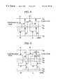
FIG. 4 is a circuit diagram showing a shift register used in an integrated circuit according to the third embodiment of the invention;
FIG. 5 is a circuit diagram showing a shift register used in an integrated circuit according to the first embodiment of the invention;
FIG. 6 is a circuit diagram showing a shift register used in an integrated circuit according to the second embodiment of the invention;
FIGS.7(A) and7(B) illustrate deteriorations of a conventional N-channel TFT;
FIG. 8 is a block diagram showing a monolithic liquid crystal display according to the first embodiment of the invention;
FIG. 9 is a block diagram showing a system according to a fourth embodiment of the invention;
FIG. 10 shows a specific configuration of the fourth embodiment; and
FIGS. 11 and 12 show examples of configurations obtained by a COG method in the fourth embodiment.
Embodiment 1
A description will be made of an embodiment in which a monolithic liquid crystal display is produced according to the present invention. FIG. 8 is a block diagram showing a monolithic liquid crystal display according to this embodiment. All of TFTs used in component circuits of a liquid crystal display, i.e., a shift register X (for a source driver), a shift register Y (for a gate driver), analog switches of the source driver, and other peripheral circuits and an active matrix circuit are of a P-channel type. FIG. 5 is a circuit diagram showing the shift register (one stage) of this embodiment.
This circuit requires three power lines VDD, VSSand VGG, where VDD>VDD. An optimum value of VGGis determined considering characteristics of the TFTs and, preferably, is approximately equal to or smaller than VSS.
Referring to FIGS.1(A)-1(E), a description will be made of a circuit manufacturing process of the above monolithic liquid crystal display. It is desirable that asubstrate 101 be made of low-alkali glass or non-alkali glass such as Corning 7059 or NA35 or NA45 of NH Technoglass Corp. To prevent the substrate from contracting in heating steps in a TFT manufacturing process, it may be subjected to a proper heat treatment in advance. A silicon dioxide film102 was formed as an undercoat film on thesubstrate 101 at a thickness of 1,000-5,000 Å, for example, 2,000 Å.
An amorphous silicon film Was further deposited at a thickness of 300-1,500 Å, for instance, 500 Å, and crystallized by thermal annealing at 500-600° C. This step may be performed by adding a very small quantity of a metal element, such as nickel, that facilitates the crystallization, to reduce the crystallization temperature, to thereby shorten the thermal annealing time. For example, when nickel was added by more than 1×10¹⁸atoms/cm3, the crystallization was completed at 550° C. in 4-8 hours. After the crystallization step, crystallinity may be improved by irradiating laser light or equivalent high-intensity light.
In the crystallization step, naturally the crystallization may be effected by pptical annealing in which the amorphous silicon film is irradiated with laser light or equivalent high-intensity light.
Then, island-like regions103-105 were formed by etching the crystallized silicon film. Theregions region 105 is used for a TFT that constitutes the active matrix circuit.
Subsequently, asilicon dioxide film 106 was deposited at a thickness of 1,000-1,500 Å, for instance, 1,200 Å by plasma CVD, and was made a gate insulating film. An aluminum film was deposited at a thickness of 3,000-8,000 Å, for instance, 5,000 Å by sputtering, and then etched into gate electrodes107-109 (see FIG.1(A)).
Then, anodic oxide films110-112 were formed on the top and side faces of the respective gate electrodes107-109 by applying a voltage in an electrolyte under the same conditions as described in Japanese Unexamined Patent Publication Nos. Hei. 5-114724 and Hei. 5-267167 (see FIG.1(B)). The thickness of the anodic oxide films110-112 was 1,500-3,000 Å, for instance, 2,000 Å. This thickness may be varied for various uses of TFTs, i.e., for TFTs used in the shift register, TFTs used in the analog buffer, TFTs used in the active matrix circuit, and TFTs for other circuits, because the thickness of the anodic oxide film is a factor of determining the width of the offset region as described in the publication No. Hei. 5-114724 and the TFT characteristics depend on the offset width.
After wiring lines connected to the gate electrodes107-109 were cut when necessary, boron was doped through the entire surface by ion doping (also palled plasma doping). A doping apparatus produced by Nissin Electric Co., Ltd. was used. The dose was 2×10¹⁴to 5×10¹⁵atoms/cm2, for instance, 5×10¹⁴atoms/cm2. The acceleration voltage was set at 30-80 kV, for instance, 65 kV, to implant ions into the silicon films103-105 through thegate insulating film 106.
After the doping, doped boron was activated by irradiating the entire surface with laser light. A KrF or XeCl excimer laser was used with an energy density of 150-350 mJ/cm2, for instance, 200 mJ/cm2. It was possible to reduce the laser energy density by heating the substrate to 200-400° C. Thus, P-type regions (sources and drains)113-115 were formed in a self-aligned manner by implanting boron into the silicon regions103-105 using the gate electrodes107-109 and the anodic oxide films110-112 as a mask (see FIG.1(C)).
Then, a silicon dioxide film or a silicon nitride film116 was deposited as an interlayer insulating film over the entire surface at a thickness of 3,000-8,000 Å, for instance, 5,000 Å. And a transparent conductive film, for instance, an indium tin oxide (ITO) film was deposited by sputtering at a thickness of 500-1,500 Å, for instance, 500 Å. Apixel electrode 117 was formed in the active matrix circuit area (pixel area) by etching the transparent conductive film (see FIG.1(D)).
After contact holes for the sources and drains113-115 of the respective TFTs and those (not shown) for the gate electrodes107-109 were formed, electrodes and wiring lines118-122 were formed in the form of a multi-layer film of a titanium nitride film and an aluminum film (see FIG.1(E)). In the above manner,TFTs 123 and124 (see FIG. 5) were formed in the peripheral drive circuit area and aTFT 125 was formed in the pixel area (see FIG.8). All of these TFTs are of a P-channel type.
Embodiment 2
A description will be made of an embodiment in which another monolithic liquid crystal display is produced according to the invention. A block diagram of a monolithic liquid crystal display of this embodiment is the same as that of FIG.8. FIG. 6 is a circuit diagram showing a shift register (one stage) of this embodiment. While all the TFTs are of a P-channel type, this embodiment has a feature that depletion type TFTs are used as loads in addition to enhancement type TFTs. In this circuit, only two power lines VDDand VSSare used; that is, the power line VGGof the first embodiment is not necessary. Therefore, this embodiment is preferable in terms of the circuit integration. The operation speed of this embodiment is generally faster than the first embodiment. The condition VDD>VSSshould also be satisfied in this embodiment.
Referring to FIGS.2(A)-2(E), a circuit manufacturing process of the above monolithic liquid crystal display will be described. Asubstrate 201 made of non-alkali glass was used. Asilicon dioxide film 202 was deposited as an undercoat film on thesubstrate 201 at a thickness of 1,000-5,000 Å, for instance, 2,000 Å.
Then, anamorphous silicon film 203 including a conductivity-imparting element such as boron or phosphorus at as low a concentration as possible was deposited at a thickness of 300-1,500 Å, for instance, 500 Å. A silicon dioxide film204 was deposited thereon at a thickness of 1,000-3,000 Å, for instance, 2,000 Å, and was masked with aphotoresist 205. The silicon dioxide film204 was formed to prevent the surface of the amorphous silicon film from being roughened by implantation of boron ions.
Subsequently, boron was selectively introduced into thesilicon film 203 by ion doping or ion implantation. In this embodiment, a weak-P-type region 206 was formed by introducing boron by ion doping in which the acceleration voltage was 65 kV and the dose was 1×10¹³to 2×10¹⁴atoms/cm2(see FIG.2(A)). A depletion type TFT would be formed in this region.
After thephotoresist mask 205 and the silicon dioxide film204 were removed, theamorphous silicon film 202 was crystallized by thermal annealing or laser light irradiation.
The crystallized silicon film was then etched into island-like regions207-209. Theregions region 209 is used for a TFT that constitutes the active matrix circuit. Theregion 207 is used for a depletion type TFT, and theregions
After a gate insulating film was deposited, gate electrodes210-212 whose top and side faces were covered with an anodic oxide film were formed in the same manner as in the first embodiment (see FIG.2(B)).
After wiring lines connected to the gate electrodes210-212 were cut when necessary, boron was doped over the entire surface by ion doping. The dose was 5×10¹⁴atoms/cm2. The acceleration voltage was set at 65 kV. After the doping, doped boron was activated by irradiating the entire surface with laser light. Thus, P-type regions (sources and drains)213-215 were formed in a self-aligned manner by implanting boron into the silicon regions207-209 using the gate electrodes210-212 and the anodic oxide films as a mask (see FIG.2(C)).
Then, a silicon dioxide film or a silicon nitride film216 was deposited as an interlayer insulating film over the entire surface at a thickness of5,000 Å. Apixel electrode 217 was formed in the active matrix circuit area (pixel area) by use of a transparent conductive film (see FIG.2(D)).
After contact holes for the sources and drains213-215 of the respective TFTs and those (not shown) for the gate electrodes210-212 were formed, electrodes and wiring lines218-222 were formed in the form of a multi-layer film of a titanium nitride film and an aluminum film (see FIG.2(E)). In the above manner,TFTs 223 and224 (see FIG. 6) were formed in the peripheral drive circuit area and aTFT 225 was formed in the pixel area. All of these TFTs are of a P-channel type. TheTFT 223 is a depletion type TFT having a weak-P-type channel-forming region. On the other hand, theTFTs
Embodiment 3
A description will be made of an embodiment in which another monolithic liquid crystal display is produced according to the invention. A block diagram of a monolithic liquid crystal display of this embodiment is the same as that of FIG.8. FIG. 4 is a circuit diagram showing a shift register (one stage) of this embodiment. While all the TFTs are of a P-channel type, this embodiment has a feature that resistors are used as loads. In this circuit, only two power lines VDDand VSSare used as in the case of the second embodiment. The operation speed of this embodiment is generally faster than the first embodiment. The condition VDD>VSSshould also be satisfied in this embodiment.
FIGS.3(A)-3(C) are sectional views of the above-type of circuits, which are manufactured by using the integrated circuit manufacturing technologies as described in the first and second embodiments. Details of a manufacturing process are omitted here.
Referring to FIG.3(A), aregion 301 is a resistor, aregion 302 is a TFT of the peripheral drive circuit, and aregion 303 is a TFT of the pixel area. An intrinsic silicon region of theregion 301 is used as a resistor. This type of resistor can be formed such that in the process of forming theTFT 123 of FIG.1(E), thegate electrode 107 is removed after the doping for forming the source and drain113 is performed. However, in this example, because intrinsic silicon is used as the resistor, the resistance value is generally large; usually more than 1 MΩ. Therefore, this example has a problem of a low circuit response speed.
Referring to FIG.3(B), aregion 304 is a resistor, aregion 305 is a TFT of the peripheral drive circuit, and aregion 306 is a TFT of the pixel area. A weak-P-type silicon region of theregion 304 is used as a resistor. This type of resistor can be formed such that in the process of forming theTFT 223 of FIG.2(E), thegate electrode 210 is removed after the doping for forming the source and drain213 is performed. In this example, because weak-P-type silicon is used as the resistor, the resistance value is usually about 100 kΩ.
Referring to FIG.3(C), aregion 307 is a resistor, aregion 308 is a TFT of the peripheral drive circuit, and aregion 309 is a TFT of the pixel area. A P-type silicon region of theregion 307 is used as a resistor. This type of resistor can be formed such that in the process of forming theTFT 123 of FIG.1(E), thegate electrode 107 is removed and then boron doping is performed. However, in this example, because P-type silicon is used as the resistor, the resistance is generally small; usually less than 10 kΩ. Therefore, this example has a problem of large power consumption.
The structure of FIG.3(C) can be formed in the step of cutting the wiring lines connected to the gate electrodes between the step (for instance, the step of FIG.1(B)) of forming the gate electrodes and performing the anodic oxidation and the boron doping step (FIG.1(C)). However, to form the structures of FIGS.3(A) and3(B), one photolithographic process should be added to remove the gate electrode after the doping.
Embodiment 4
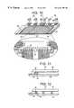
The first to third embodiments are directed only to the monolithic active matrix liquid crystal display. It is apparently possible to construct a more advanced system by using the active matrix liquid crystal display thus formed. FIG. 9 is a block diagram showing an example of such a system.
In the example of FIG. 9, the reduction in size, weight and thickness is attained by fixing semiconductor chips that are usually mounted on a computer main board on at least one of a pair of substrates of a liquid crystal display which substrates hold a liquid crystal. In particular, the above chips are fixed on the substrate having an active matrix circuit. The invention has a disadvantage that since P-channel TFTs is used in an active Matrix circuit and peripheral drive circuits, the power consumption is larger than in the case of using ordinary CMOS peripheral drive circuits. Therefore, in the system under discussion, the chips other than the liquid crystal display panel should use CMOS transistors, to reduce the power consumption. The substrate having the active matrix circuit uses the monolithic active matrix circuit of the invention.
A description will be made of the system of FIG. 9. Asubstrate 15 also serves as a substrate of a liquid crystal display. Anactive matrix circuit 14 having a large number of pixels each including aTFT 11, apixel electrode 12 and anauxiliary capacitor 13, and an X decoder/driver, a Y decoder/driver and an XY branching circuit for driving the active matrix circuit are formed on thesubstrate 15 by using TFTs.
In this embodiment, other chips are additionally mounted on thesubstrate 15. These chips are connected to the circuits on thesubstrate 15 by wire bonding, a COG (chip one glass) method, or some other means. In FIG. 9, a correction memory, a memory, a CPU, and an input port are chips that are mounted in such a manner. Other various chips may be mounted on thesubstrate 15.
In FIG. 9, the input port is a circuit for reading an externally input signal. The correction memory is a memory for correcting an input signal etc. in accordance with the active matrix panel, and is therefore dedicated to the panel. More specifically, the correction memory is a nonvolatile memory that contains information specific to each pixel, and serves to effect correction for each pixel. Where a point defect exists at a certain pixel of an electro-optical device, signals corrected for the defective pixel are supplied to pixels adjacent thereto, to thereby compensate for the point defect and make it less discernible. Where a certain pixel is darker than adjacent pixels, a larger signal is supplied to that pixel to make its brightness equal to that of the adjacent pixels. Since the information on pixel defects is different from one panel to another, the information stored in the correction memory varies with the panel.
The CPU and the memory have the same functions as those used in ordinary computers. In particular, the memory has, as a RAM, an image memory corresponding to the pixels. All of these chips are of a CMOS type.
FIG. 10 shows an example of a specific configuration of this embodiment.Substrates active matrix circuit 21 and peripheral drive circuits22-24 for driving it were formed on thesubstrate 20 by using TFTs. Amain memory chip 26, an MPU (microprocessing unit)27, acorrection memory 28 were bonded to the surface on which the above circuits are formed, and these chips were connected to the circuits on thesubstrate 20. For example, when the chips were to be connected by a COG (chip on glass) method, wiring lines as denoted by29 in FIG. 10 were formed in a fixingportion 25 on thesubstrate 20.
FIGS. 11 and 12 show specific shapes of contacts. In the method of FIG. 11, aconductive bump 34 provided at anelectrode portion 33 of achip 32 Was brought into contact with awiring line 31 on asubstrate 30, and anorganic resin 35 was introduced into a space between thechip 32 and thesubstrate 30 for fixing those to each other. Thebump 34 may be made of gold formed by electroless plating.
In the method of FIG. 12, achip 42 and asubstrate 40 were bonded each other with an organic resin in which conductive particles (for example, gold particles)44 were dispersed. Thechip 42 was connected to the circuits by contacting anelectrode portion 43 of thechip 42 and awiring line 41 on the substrate to theconductive particles 44 existing therebetween. The organic resin used for the bonding was of an optical setting type, thermosetting type, or natural setting type. The liquid crystal may be injected into the liquid crystal display after the chip bonding.
Even the CPU and the memory were formed on the liquid crystal display substrate by the above process, so that an electronic device such as a simple personal computer could be constructed on a single substrate.
The chips may be connected to the circuits by a known wire bonding method.
The invention can improve the reliability of the monolithic active matrix circuit. Further, the invention can make the manufacturing process simpler than the process in the case of forming an ordinary CMOS circuit. For example, a photolithographic step for doping a different kind of impurities and a step of implanting N-type impurities, which are necessary in forming a CMOS circuit, are eliminated in the first embodiment.
The second embodiment needs the same number of steps as in the case of forming an ordinary CMOS circuit, because a photolithographic step and a doping step are needed to form the weak-P-type region. However, where a photoresist or the like is used as a doping mask and ions are doped at a high dose, a long-term ashing step is usually needed because of difficulty in removing the carbonized photoresist. In contrast, in the second embodiment, the dose itself is low and thephotoresist 205 can be removed by a lift-off method by etching the silicon dioxide film204 (see FIG.2(A)). Therefore, the photoresist mask can be removed more easily after the doping than in the process of forming an ordinary CMOS circuit.
As described above, the invention is useful from the industrial point of view.
Claims (56)
1. A semiconductor device comprising:
a plurality of first thin film transistors for switching pixels formed over a substrate having an insulating surface;
a driver circuit comprising a plurality of second thin film transistors formed over said substrate for driving said first thin film transistors, each of said first and second thin film transistors having a channel forming region comprising crystalline silicon;
an interlayer insulating film formed over said first thin film transistors and said second thin film transistors;
a plurality of pixel electrodes formed on said interlayer insulating film and electrically connected to said first thin film transistors at one of source or drain thereof;
a plurality of wirings formed on said interlayer insulating film and electrically connected to said first thin film transistors at the other one of the source or drain thereof,
wherein all of said first and second thin film transistors are p-channel type thin film transistors.
2. The semiconductor device according toclaim 1 wherein said driver circuit comprises a shift register.
3. The semiconductor device according toclaim 1 wherein at least one of said second thin film transistors has its channel region doped with boron and at least another one of said second thin film transistors has its channel region not doped with boron.
4. The semiconductor device according toclaim 1 wherein said pixel electrodes are transparent.
5. The semiconductor device according toclaim 1 wherein said interlayer insulating film comprises silicon oxide.
6. The semiconductor device according toclaim 1 wherein said interlayer insulating film comprises silicon nitride.
7. A semiconductor device comprising:
a plurality of first thin film transistors for switching pixels, formed over a substrate having an insulating surface;
a driver circuit comprising a plurality of second thin film transistors formed over said substrate for driving said first thin film transistors, each of said first and second thin film transistors comprising a crystalline semiconductor layer having source and drain regions and a channel forming region extending therebetween, a gate insulating film formed on said channel forming region and a gate electrode formed on said gate insulating film;
an interlayer insulating film formed over said first thin film transistors and said second thin film transistors;
a plurality of pixel electrodes formed on said interlayer insulating film and electrically connected to said first thin film transistors at one of source or drain thereof;
a plurality of wirings formed on said interlayer insulating film and electrically connected to said first thin film transistors at the other one of the source or drain thereof,
wherein all of said first and second thin film transistors are p-channel type film transistors.
8. The semiconductor device according toclaim 7 wherein said driver circuit comprises a shift register.
9. The semiconductor device according toclaim 7 wherein at least one of said second thin film transistors has its channel region doped with boron and at least another one of said second thin film transistors has its channel region not doped with boron.
10. The semiconductor device according toclaim 7 wherein said pixel electrodes are transparent.
11. The semiconductor device according toclaim 7 wherein said interlayer insulating film comprises silicon oxide.
12. The semiconductor device according toclaim 7 wherein said interlayer insulating film comprises silicon nitride.
13. A semiconductor device comprising:
a plurality of first thin film transistors for switching pixels formed over a substrate having an insulating surface;
a driver circuit comprising a plurality of second thin film transistors formed over said substrate for driving said first thin film transistors, each of said first and second thin film transistors having a channel forming region comprising crystalline silicon;
an interlayer insulating film formed over said first thin film transistors and said second thin film transistors;
a plurality of pixel electrodes formed on said interlayer insulating film and electrically connected to said first thin film transistors at one of source or drain thereof;
a plurality of wirings formed on said interlayer insulating film and electrically connected to said first thin film transistors at the other one of the source or drain thereof; and
a semiconductor chip formed over the substrate,
wherein all of said first and second thin film transistors are p-channel type thin film transistors.
14. The semiconductor device according toclaim 13 wherein said driver circuit comprises a shift register.
15. The semiconductor device according toclaim 13 wherein at least one of said second thin film transistors has its channel region doped with boron and at least another one of said second thin film transistors has its channel region not doped with boron.
16. The semiconductor device according toclaim 13 wherein said pixel electrodes are transparent.
17. The semiconductor device according toclaim 13 wherein said interlayer insulating film comprises silicon oxide.
18. The semiconductor device according toclaim 13 wherein said interlayer insulating film comprises silicon nitride.
19. The semiconductor device according toclaim 13 wherein each of said first and second thin film transistors has an offset structure.
20. The semiconductor device according toclaim 13 wherein said semiconductor chip is at least one of a correction memory, a memory, a CPU and an input port.
21. The semiconductor device according toclaim 13 wherein each of said first and second thin film transistor has a gate electrode over the channel forming region.
22. A semiconductor device comprising:
a plurality of first thin film transistors for switching pixels formed over a substrate having an insulating surface;
a driver circuit comprising a plurality of second thin film transistors formed over said substrate for driving said first thin film transistors, each of said first and second thin film transistors having a channel forming region comprising crystalline silicon;
an interlayer insulating film formed over said first thin film transistors and said second thin film transistors;
a plurality of pixel electrodes formed on said interlayer insulating film and electrically connected to said first thin film transistors at one of source or drain thereof;
a plurality of conductors formed on said interlayer insulating film and electrically connected to said first thin film transistors at the other one of the source or drain thereof,
wherein all of said first and second thin film transistors are p-channel type thin film transistors.
23. The semiconductor device according toclaim 22 wherein said pixel electrodes are transparent.
24. The semiconductor device according toclaim 22 wherein said interlayer insulating film comprises silicon oxide.
25. The semiconductor device according toclaim 22 wherein said interlayer insulating film comprises silicon nitride.
26. The semiconductor device according toclaim 22 wherein each of said first and second thin film transistors has an offset structure.
27. The semiconductor device according toclaim 22 further comprising a semiconductor chip formed over the substrate.
28. The semiconductor device according toclaim 22 wherein each of said first and second thin film transistor has a gate electrode over the channel forming region.
29. A semiconductor device comprising:
a plurality of first thin film transistors for switching pixels formed over a substrate having an insulating surface;
a source driver circuit comprising a plurality of second thin film transistors formed over said substrate, each of said first and second thin film transistors having a channel forming region comprising crystalline silicon;
an interlayer insulating film formed over said first thin film transistors and said second thin film transistors;
a plurality of pixel electrodes formed on said interlayer insulating film and electrically connected to said first thin film transistors at one of source or drain thereof;
a plurality of conductors formed on said interlayer insulating film and electrically connected to said first thin film transistors at the other one of the source or drain thereof,
wherein all of said first and second thin film transistors are p-channel type thin film transistors.
30. The semiconductor device according toclaim 29 wherein said pixel electrodes are transparent.
31. The semiconductor device according toclaim 29 wherein said interlayer insulating film comprises silicon oxide.
32. The semiconductor device according toclaim 29 wherein said interlayer insulating film comprises silicon nitride.
33. The semiconductor device according toclaim 29 wherein each of said first and second thin film transistors has an offset structure.
34. The semiconductor device according toclaim 29 further comprising a semiconductor chip formed over the substrate.
35. The semiconductor device according toclaim 29 wherein each of said first and second thin film transistor has a gate electrode over the channel forming region.
36. A semiconductor device comprising:
a plurality of first thin film transistors for switching pixels formed over a substrate having an insulating surface;
a gate driver circuit comprising a plurality of second thin film transistors formed over said substrate, each of said first and second thin film transistors having a channel forming region comprising crystalline silicon;
an interlayer insulating film formed over said first thin film transistors and said second thin film transistors;
a plurality of pixel electrodes formed on said interlayer insulating film and electrically connected to said first thin film transistors at one of source or drain thereof;
a plurality of conductors formed on said interlayer insulating film and electrically connected to said first thin film transistors at the other one of the source or drain thereof,
wherein all of said first and second thin film transistors are p-channel type thin film transistors.
37. The semiconductor device according toclaim 36 wherein said pixel electrodes are transparent.
38. The semiconductor device according toclaim 36 wherein said interlayer insulating film comprises silicon oxide.
39. The semiconductor device according toclaim 36 wherein said interlayer insulating film comprises silicon nitride.
40. The semiconductor device according toclaim 36 wherein each of said first and second thin film transistors has an offset structure.
41. The semiconductor device according toclaim 36 further comprising a semiconductor chip formed over the substrate.
42. The semiconductor device according toclaim 36 wherein each of said first and second thin film transistor has a gate electrode over the channel forming region.
43. A semiconductor device comprising:
a plurality of first thin film transistors for switching pixels formed over a substrate having an insulating surface;
a source driver circuit comprising a plurality of second thin film transistors formed over said substrate, each of said first and second thin film transistors having a channel forming region comprising crystalline silicon;
an interlayer insulating film formed over said first thin film transistors and said second thin film transistors;
a plurality of pixel electrodes formed on said interlayer insulating film and electrically connected to said first thin film transistors at one of source or drain thereof;
a plurality of wirings formed on said interlayer insulating film and electrically connected to said first thin film transistors at the other one of the source or drain thereof,
wherein all of said first and second thin film transistors are p-channel type thin film transistors.
44. The semiconductor device according toclaim 43 wherein said pixel electrodes are transparent.
45. The semiconductor device according toclaim 43 wherein said interlayer insulating film comprises silicon oxide.
46. The semiconductor device according toclaim 43 wherein said interlayer insulating film comprises silicon nitride.
47. The semiconductor device according toclaim 43 wherein each of said first and second thin film transistors has an offset structure.
48. The semiconductor device according toclaim 43 further comprising a semiconductor chip formed over the substrate.
49. The semiconductor device according toclaim 43 wherein each of said first and second thin film transistor has a gate electrode over the channel forming region.
50. A semiconductor device comprising:
a plurality of first thin film transistors for switching pixels formed over a substrate having an insulating surface;
a gate driver circuit comprising a plurality of second thin film transistors formed over said substrate, each of said first and second thin film transistors having a channel forming region comprising crystalline silicon;
an interlayer insulating film formed over said first thin film transistors and said second thin film transistors;
a plurality of pixel electrodes formed on said interlayer insulating film and electrically connected to said first thin film transistors at one of source or drain thereof;
a plurality of wirings formed on said interlayer insulating film and electrically connected to said first thin film transistors at the other one of the source or drain thereof,
wherein all of said first and second thin film transistors are p-channel type thin film transistors.
51. The semiconductor device according toclaim 50 wherein said pixel electrodes are transparent.
52. semiconductor device according toclaim 50 wherein said interlayer insulating film comprises silicon oxide.
53. The semiconductor device according toclaim 50 wherein said interlayer insulating film comprises silicon nitride.
54. The semiconductor device according toclaim 50 wherein each of said first and second thin film transistors has an offset structure.
55. The semiconductor device according toclaim 50 further comprising a semiconductor chip formed over the substrate.
56. The semiconductor device according toclaim 50 wherein each of said first and second thin film transistor has a gate electrode over the channel forming region.
Priority Applications (3)
| Application Number | Priority Date | Filing Date | Title |
|---|---|---|---|
| US09/229,677US6441399B1 (en) | 1994-04-22 | 1999-01-13 | Semiconductor integrated system |
| US10/202,873US7145173B2 (en) | 1994-04-22 | 2002-07-26 | Semiconductor integrated circuit |
| US10/939,973US7166862B2 (en) | 1994-04-22 | 2004-09-14 | Semiconductor integrated circuit |
Applications Claiming Priority (5)
| Application Number | Priority Date | Filing Date | Title |
|---|---|---|---|
| JP6-107575 | 1994-04-22 | ||
| JP10757594AJP3402400B2 (en) | 1994-04-22 | 1994-04-22 | Manufacturing method of semiconductor integrated circuit |
| US42308595A | 1995-04-18 | 1995-04-18 | |
| US08/688,829US5889291A (en) | 1994-04-22 | 1996-07-31 | Semiconductor integrated circuit |
| US09/229,677US6441399B1 (en) | 1994-04-22 | 1999-01-13 | Semiconductor integrated system |
Related Parent Applications (1)
| Application Number | Title | Priority Date | Filing Date |
|---|---|---|---|
| US08/688,829DivisionUS5889291A (en) | 1994-04-22 | 1996-07-31 | Semiconductor integrated circuit |
Related Child Applications (1)
| Application Number | Title | Priority Date | Filing Date |
|---|---|---|---|
| US10/202,873DivisionUS7145173B2 (en) | 1994-04-22 | 2002-07-26 | Semiconductor integrated circuit |
Publications (1)
| Publication Number | Publication Date |
|---|---|
| US6441399B1true US6441399B1 (en) | 2002-08-27 |
Family
ID=14462656
Family Applications (5)
| Application Number | Title | Priority Date | Filing Date |
|---|---|---|---|
| US08/688,829Expired - LifetimeUS5889291A (en) | 1994-04-22 | 1996-07-31 | Semiconductor integrated circuit |
| US09/229,677Expired - LifetimeUS6441399B1 (en) | 1994-04-22 | 1999-01-13 | Semiconductor integrated system |
| US09/229,676Expired - Fee RelatedUS6599791B1 (en) | 1994-04-22 | 1999-01-13 | Semiconductor integrated circuit |
| US10/202,873Expired - Fee RelatedUS7145173B2 (en) | 1994-04-22 | 2002-07-26 | Semiconductor integrated circuit |
| US10/939,973Expired - Fee RelatedUS7166862B2 (en) | 1994-04-22 | 2004-09-14 | Semiconductor integrated circuit |
Family Applications Before (1)
| Application Number | Title | Priority Date | Filing Date |
|---|---|---|---|
| US08/688,829Expired - LifetimeUS5889291A (en) | 1994-04-22 | 1996-07-31 | Semiconductor integrated circuit |
Family Applications After (3)
| Application Number | Title | Priority Date | Filing Date |
|---|---|---|---|
| US09/229,676Expired - Fee RelatedUS6599791B1 (en) | 1994-04-22 | 1999-01-13 | Semiconductor integrated circuit |
| US10/202,873Expired - Fee RelatedUS7145173B2 (en) | 1994-04-22 | 2002-07-26 | Semiconductor integrated circuit |
| US10/939,973Expired - Fee RelatedUS7166862B2 (en) | 1994-04-22 | 2004-09-14 | Semiconductor integrated circuit |
Country Status (3)
| Country | Link |
|---|---|
| US (5) | US5889291A (en) |
| JP (1) | JP3402400B2 (en) |
| KR (3) | KR100416875B1 (en) |
Cited By (24)
| Publication number | Priority date | Publication date | Assignee | Title |
|---|---|---|---|---|
| US20010017372A1 (en)* | 2000-02-29 | 2001-08-30 | Semiconductor Energy Laboratory Co., Ltd. | Display device and method for fabricating the same |
| US6559477B2 (en)* | 2000-09-29 | 2003-05-06 | Kabushiki Kaisha Toshiba | Flat panel display device and method for manufacturing the same |
| US20030178682A1 (en)* | 2001-12-28 | 2003-09-25 | Takeshi Noda | Semiconductor device and method of manufacturing the semiconductor device |
| US6638869B2 (en)* | 2001-02-21 | 2003-10-28 | Au Optronics Corp. | Process for manufacturing reflective TFT-LCD with rough diffuser |
| US20040046174A1 (en)* | 1996-06-04 | 2004-03-11 | Semiconductor Energy Laboratory Co., Ltd., A Japan Corporation | Semiconductor integrated circuit and fabrication method thereof |
| US20040141139A1 (en)* | 1995-02-15 | 2004-07-22 | Semiconductor Energy Laboratory Co., Ltd., A Japan Corporation | Active matrix display and forming method thereof |
| US6778164B2 (en) | 1997-08-20 | 2004-08-17 | Semiconductor Energy Laboratory Co., Ltd. | Electrooptical device |
| US20040188761A1 (en)* | 2003-03-26 | 2004-09-30 | Semiconductor Energy Laboratory Co., Ltd. | Source follower circuit or bootstrap circuit, driver circuit comprising such circuit, and display device comprising such driver circuit |
| US20050092996A1 (en)* | 2001-02-28 | 2005-05-05 | Semiconductor Energy Laboratory Co., Ltd., A Japan Corporation | Semiconductor device and manufacturing method thereof |
| US20050139831A1 (en)* | 1994-04-22 | 2005-06-30 | Semiconductor Energy | Semiconductor integrated circuit |
| US20060163574A1 (en)* | 2000-03-08 | 2006-07-27 | Semiconductor Energy Laboratory Co., Ltd. | Semiconductor device and manufacturing method thereof |
| USRE40028E1 (en)* | 1999-05-27 | 2008-01-22 | Lg. Philips Lcd Co., Ltd. | Liquid crystal display device and method of manufacturing the same |
| US20090046049A1 (en)* | 1994-04-22 | 2009-02-19 | Semiconductor Energy Laboratory Co., Ltd. | Redundancy shift register circuit for driver circuit in active matrix type liquid crystal display device |
| US7633471B2 (en) | 2000-05-12 | 2009-12-15 | Semiconductor Energy Laboratory Co., Ltd. | Light-emitting device and electric appliance |
| US7642559B2 (en) | 1999-06-04 | 2010-01-05 | Semiconductor Energy Laboratory Co., Ltd. | Electro-optical device and electronic device |
| US7656491B2 (en) | 2000-03-16 | 2010-02-02 | Semiconductor Energy Laboratory Co., Ltd. | Liquid crystal display device and method of manufacturing the same |
| US7687325B2 (en) | 2000-03-13 | 2010-03-30 | Semiconductor Energy Laboratory Co., Ltd. | Semiconductor device and manufacturing method thereof |
| US7705354B2 (en) | 2000-03-06 | 2010-04-27 | Semiconductor Energy Laboratory Co., Ltd | Semiconductor device and method for fabricating the same |
| US7714975B1 (en) | 2000-03-17 | 2010-05-11 | Semiconductor Energy Laboratory Co., Ltd | Liquid crystal display device and manfacturing method thereof |
| US7714329B2 (en) | 2001-03-06 | 2010-05-11 | Semiconductor Energy Laboratory Co., Ltd. | Semiconductor device having thin film transistor |
| US7902550B2 (en) | 2000-05-09 | 2011-03-08 | Semiconductor Energy Laboratory Co., Ltd. | Semiconductor device and manufacturing method thereof |
| US8300201B2 (en) | 2000-03-13 | 2012-10-30 | Semiconductor Energy Laboratory Co., Ltd. | Semiconductor device and a method of manufacturing the same |
| US20130126883A1 (en)* | 1999-06-22 | 2013-05-23 | Semiconductor Energy Laboratory Co., Ltd. | Wiring Material, Semiconductor Device Provided with a Wiring Using the Wiring Material and Method of Manufacturing Thereof |
| US9048147B2 (en) | 2008-09-30 | 2015-06-02 | Semiconductor Energy Laboratory Co., Ltd. | Display device |
Families Citing this family (59)
| Publication number | Priority date | Publication date | Assignee | Title |
|---|---|---|---|---|
| US7115902B1 (en) | 1990-11-20 | 2006-10-03 | Semiconductor Energy Laboratory Co., Ltd. | Electro-optical device and method for manufacturing the same |
| US5849601A (en) | 1990-12-25 | 1998-12-15 | Semiconductor Energy Laboratory Co., Ltd. | Electro-optical device and method for manufacturing the same |
| KR950013784B1 (en) | 1990-11-20 | 1995-11-16 | 가부시키가이샤 한도오따이 에네루기 겐큐쇼 | Field effect trasistor and its making method and tft |
| US7098479B1 (en) | 1990-12-25 | 2006-08-29 | Semiconductor Energy Laboratory Co., Ltd. | Electro-optical device and method for manufacturing the same |
| US7576360B2 (en)* | 1990-12-25 | 2009-08-18 | Semiconductor Energy Laboratory Co., Ltd. | Electro-optical device which comprises thin film transistors and method for manufacturing the same |
| CN1244891C (en)* | 1992-08-27 | 2006-03-08 | 株式会社半导体能源研究所 | Active matrix display |
| US7081938B1 (en)* | 1993-12-03 | 2006-07-25 | Semiconductor Energy Laboratory Co., Ltd. | Electro-optical device and method for manufacturing the same |
| US6906383B1 (en)* | 1994-07-14 | 2005-06-14 | Semiconductor Energy Laboratory Co., Ltd. | Semiconductor device and method of manufacture thereof |
| CN100576306C (en)* | 1995-02-01 | 2009-12-30 | 精工爱普生株式会社 | Liquid crystal display device |
| JP3640224B2 (en)* | 1996-06-25 | 2005-04-20 | 株式会社半導体エネルギー研究所 | LCD panel |
| US7298447B1 (en) | 1996-06-25 | 2007-11-20 | Semiconductor Energy Laboratory Co., Ltd. | Liquid crystal display panel |
| JP3525316B2 (en)* | 1996-11-12 | 2004-05-10 | 株式会社半導体エネルギー研究所 | Active matrix display |
| JPH11160734A (en)* | 1997-11-28 | 1999-06-18 | Semiconductor Energy Lab Co Ltd | Liquid crystal electrooptical device |
| US5998805A (en)* | 1997-12-11 | 1999-12-07 | Motorola, Inc. | Active matrix OED array with improved OED cathode |
| JP2001119029A (en)* | 1999-10-18 | 2001-04-27 | Fujitsu Ltd | Thin film transistor, method of manufacturing the same, and liquid crystal display device having the same |
| US6825488B2 (en)* | 2000-01-26 | 2004-11-30 | Semiconductor Energy Laboratory Co., Ltd. | Semiconductor device and manufacturing method thereof |
| JP5183838B2 (en)* | 2000-05-12 | 2013-04-17 | 株式会社半導体エネルギー研究所 | Light emitting device |
| JP4649706B2 (en)* | 2000-06-08 | 2011-03-16 | ソニー株式会社 | Display device and portable terminal using the same |
| JP2012089878A (en)* | 2000-08-25 | 2012-05-10 | Semiconductor Energy Lab Co Ltd | Light-emitting device |
| KR100737910B1 (en)* | 2000-11-27 | 2007-07-10 | 삼성전자주식회사 | Polysilicon Thin Film Transistor Manufacturing Method |
| TW525216B (en) | 2000-12-11 | 2003-03-21 | Semiconductor Energy Lab | Semiconductor device, and manufacturing method thereof |
| SG111923A1 (en)* | 2000-12-21 | 2005-06-29 | Semiconductor Energy Lab | Light emitting device and method of manufacturing the same |
| JP4593256B2 (en)* | 2001-02-28 | 2010-12-08 | 株式会社半導体エネルギー研究所 | Method for manufacturing semiconductor device |
| JP4079655B2 (en)* | 2001-02-28 | 2008-04-23 | 株式会社半導体エネルギー研究所 | Semiconductor device and manufacturing method thereof |
| JP2002353245A (en)* | 2001-03-23 | 2002-12-06 | Seiko Epson Corp | Electro-optical substrate device and method of manufacturing the same, electro-optical device, electronic equipment, and method of manufacturing substrate device |
| KR100426380B1 (en)* | 2001-03-30 | 2004-04-08 | 주승기 | Method of crystallizing a silicon layer and method of fabricating a semiconductor device using the same |
| JP4785271B2 (en)* | 2001-04-27 | 2011-10-05 | 株式会社半導体エネルギー研究所 | Liquid crystal display device, electronic equipment |
| JP4439761B2 (en) | 2001-05-11 | 2010-03-24 | 株式会社半導体エネルギー研究所 | Liquid crystal display device, electronic equipment |
| TW582005B (en)* | 2001-05-29 | 2004-04-01 | Semiconductor Energy Lab | Pulse output circuit, shift register, and display device |
| SG148032A1 (en)* | 2001-07-16 | 2008-12-31 | Semiconductor Energy Lab | Light emitting device |
| US6788108B2 (en) | 2001-07-30 | 2004-09-07 | Semiconductor Energy Laboratory Co., Ltd. | Semiconductor device |
| JP4831895B2 (en)* | 2001-08-03 | 2011-12-07 | 株式会社半導体エネルギー研究所 | Semiconductor device |
| US7218349B2 (en)* | 2001-08-09 | 2007-05-15 | Semiconductor Energy Laboratory Co., Ltd. | Semiconductor device |
| JP4869516B2 (en) | 2001-08-10 | 2012-02-08 | 株式会社半導体エネルギー研究所 | Semiconductor device |
| JP4397555B2 (en)* | 2001-11-30 | 2010-01-13 | 株式会社半導体エネルギー研究所 | Semiconductor devices, electronic equipment |
| JP2003330388A (en)* | 2002-05-15 | 2003-11-19 | Semiconductor Energy Lab Co Ltd | Semiconductor device and manufacturing method thereof |
| JP4736313B2 (en)* | 2002-09-10 | 2011-07-27 | 日本電気株式会社 | Thin film semiconductor device |
| US7094684B2 (en)* | 2002-09-20 | 2006-08-22 | Semiconductor Energy Laboratory Co., Ltd. | Manufacturing method of semiconductor device |
| TWI338346B (en) | 2002-09-20 | 2011-03-01 | Semiconductor Energy Lab | Display device and manufacturing method thereof |
| JP4339103B2 (en) | 2002-12-25 | 2009-10-07 | 株式会社半導体エネルギー研究所 | Semiconductor device and display device |
| JP4480968B2 (en)* | 2003-07-18 | 2010-06-16 | 株式会社半導体エネルギー研究所 | Display device |
| JP4393812B2 (en)* | 2003-07-18 | 2010-01-06 | 株式会社半導体エネルギー研究所 | Display device and electronic device |
| US7566001B2 (en)* | 2003-08-29 | 2009-07-28 | Semiconductor Energy Laboratory Co., Ltd. | IC card |
| KR101021715B1 (en)* | 2004-03-06 | 2011-03-15 | 엘지디스플레이 주식회사 | Manufacturing method of liquid crystal display device with improved storage doping process |
| US9153341B2 (en) | 2005-10-18 | 2015-10-06 | Semiconductor Energy Laboratory Co., Ltd. | Shift register, semiconductor device, display device, and electronic device |
| US7781768B2 (en)* | 2006-06-29 | 2010-08-24 | Semiconductor Energy Laboratory Co., Ltd. | Display device, method for manufacturing the same, and electronic device having the same |
| JP2007134730A (en)* | 2006-12-01 | 2007-05-31 | Semiconductor Energy Lab Co Ltd | Display device |
| US8044499B2 (en)* | 2008-06-10 | 2011-10-25 | Semiconductor Energy Laboratory Co., Ltd. | Wiring substrate, manufacturing method thereof, semiconductor device, and manufacturing method thereof |
| EP2515337B1 (en)* | 2008-12-24 | 2016-02-24 | Semiconductor Energy Laboratory Co., Ltd. | Driver circuit and semiconductor device |
| US9715845B2 (en) | 2009-09-16 | 2017-07-25 | Semiconductor Energy Laboratory Co., Ltd. | Semiconductor display device |
| KR102143040B1 (en) | 2009-10-16 | 2020-08-11 | 가부시키가이샤 한도오따이 에네루기 켄큐쇼 | Liquid crystal display device and electronic apparatus having the same |
| KR102329497B1 (en)* | 2009-11-13 | 2021-11-22 | 가부시키가이샤 한도오따이 에네루기 켄큐쇼 | Display device and electronic device including the same |
| JP4877413B2 (en)* | 2010-10-28 | 2012-02-15 | ソニー株式会社 | Display device and portable terminal using the same |
| KR101895326B1 (en)* | 2011-05-13 | 2018-09-05 | 가부시키가이샤 한도오따이 에네루기 켄큐쇼 | Display device |
| CN102646717B (en)* | 2012-02-29 | 2015-01-21 | 京东方科技集团股份有限公司 | Array substrate, manufacturing method thereof and display device |
| JP5613810B2 (en)* | 2013-09-27 | 2014-10-29 | 株式会社半導体エネルギー研究所 | Display device |
| KR102617041B1 (en) | 2015-12-28 | 2023-12-26 | 가부시키가이샤 한도오따이 에네루기 켄큐쇼 | devices, television systems, and electronic devices |
| US12040795B2 (en) | 2018-12-20 | 2024-07-16 | Semiconductor Energy Laboratory Co., Ltd. | Logic circuit formed using unipolar transistor, and semiconductor device |
| TWI822833B (en) | 2019-08-15 | 2023-11-21 | 優顯科技股份有限公司 | Electronic detection interface, electronic detection module using the same, and electronic detection method applicable of the same |
Citations (123)
| Publication number | Priority date | Publication date | Assignee | Title |
|---|---|---|---|---|
| US3806778A (en) | 1971-12-24 | 1974-04-23 | Nippon Electric Co | Insulated-gate field effect semiconductor device having low and stable gate threshold voltage |
| US3820108A (en) | 1972-03-10 | 1974-06-25 | Optel Corp | Decoder and driver circuits particularly adapted for use with liquid crystal displays |
| US3935083A (en) | 1973-01-12 | 1976-01-27 | Hitachi, Ltd. | Method of forming insulating film on interconnection layer |
| US3988616A (en)* | 1974-07-15 | 1976-10-26 | Hitachi, Ltd. | Driver circuit for liquid crystal display using insulated gate FETs |
| US3988214A (en) | 1968-06-17 | 1976-10-26 | Nippon Electric Company, Ltd. | Method of fabricating a semiconductor device |
| US4232327A (en) | 1978-11-13 | 1980-11-04 | Rca Corporation | Extended drain self-aligned silicon gate MOSFET |
| US4357179A (en) | 1980-12-23 | 1982-11-02 | Bell Telephone Laboratories, Incorporated | Method for producing devices comprising high density amorphous silicon or germanium layers by low pressure CVD technique |
| US4368523A (en) | 1979-12-20 | 1983-01-11 | Tokyo Shibaura Denki Kabushiki Kaisha | Liquid crystal display device having redundant pairs of address buses |
| US4380008A (en) | 1978-09-29 | 1983-04-12 | Hitachi, Ltd. | Method of driving a matrix type phase transition liquid crystal display device to obtain a holding effect and improved response time for the erasing operation |
| US4409724A (en) | 1980-11-03 | 1983-10-18 | Texas Instruments Incorporated | Method of fabricating display with semiconductor circuits on monolithic structure and flat panel display produced thereby |
| US4413256A (en) | 1980-02-21 | 1983-11-01 | Sharp Kabushiki Kaisha | Driving method for display panels |
| US4468855A (en) | 1981-08-05 | 1984-09-04 | Fujitsu Limited | Method of making aluminum gate self-aligned FET by selective beam annealing through reflective and antireflective coatings |
| US4470060A (en) | 1981-01-09 | 1984-09-04 | Semiconductor Energy Laboratory Co., Ltd. | Liquid crystal display with vertical non-single crystal semiconductor field effect transistors |
| US4525436A (en) | 1982-03-29 | 1985-06-25 | Semiconductor Energy Laboratory Co., Ltd. | Light energy conversion system |
| US4557036A (en) | 1982-03-31 | 1985-12-10 | Nippon Telegraph & Telephone Public Corp. | Semiconductor device and process for manufacturing the same |
| US4597160A (en) | 1985-08-09 | 1986-07-01 | Rca Corporation | Method of fabricating a polysilicon transistor with a high carrier mobility |
| US4605972A (en) | 1983-09-05 | 1986-08-12 | Fuji Photo Film Co., Ltd. | Image forming method |
| US4641156A (en) | 1983-12-30 | 1987-02-03 | Casio Computer Co., Ltd. | Recording apparatus with double frequency driven liquid crystal shutter |
| US4646426A (en) | 1981-02-16 | 1987-03-03 | Fujitsu Limited | Method of producing MOS FET type semiconductor device |
| US4693770A (en) | 1985-07-05 | 1987-09-15 | Matsushita Electric Industrial Co., Ltd. | Method of bonding semiconductor devices together |
| US4709993A (en) | 1985-12-18 | 1987-12-01 | Hitachi, Ltd. | Liquid crystal color display device having plural color filters per segment electrode |
| US4716403A (en) | 1982-10-01 | 1987-12-29 | Seiko Epson Kabushiki Kaisha | Liquid crystal display device |
| US4727044A (en) | 1984-05-18 | 1988-02-23 | Semiconductor Energy Laboratory Co., Ltd. | Method of making a thin film transistor with laser recrystallized source and drain |
| US4728617A (en) | 1986-11-04 | 1988-03-01 | Intel Corporation | Method of fabricating a MOSFET with graded source and drain regions |
| US4746628A (en) | 1983-08-26 | 1988-05-24 | Sharp Kabushiki Kaisha | Method for making a thin film transistor |
| US4757028A (en) | 1985-10-07 | 1988-07-12 | Agency Of Industrial Science And Technology | Process for preparing a silicon carbide device |
| US4762806A (en) | 1983-12-23 | 1988-08-09 | Sharp Kabushiki Kaisha | Process for producing a SiC semiconductor device |
| US4762807A (en) | 1984-03-05 | 1988-08-09 | Semiconductor Energy Laboratory Co., Ltd. | Method for making a non-single crystal insulated-gate field effect transistor |
| US4769713A (en) | 1986-07-30 | 1988-09-06 | Hosiden Electronics Co. Ltd. | Method and apparatus for multi-gradation display |
| US4772927A (en) | 1985-10-23 | 1988-09-20 | Hitachi, Ltd. | Thin film FET doped with diffusion inhibitor |
| US4775641A (en) | 1986-09-25 | 1988-10-04 | General Electric Company | Method of making silicon-on-sapphire semiconductor devices |
| US4783143A (en) | 1986-03-07 | 1988-11-08 | Siemens Aktiengesellschaft | Method for suitably positioning light waveguides for coupling locations and for coupling elements in a light waveguide switch |
| US4803530A (en)* | 1977-08-22 | 1989-02-07 | Shinji Taguchi | Semiconductor integrated circuit formed on an insulator substrate |
| US4804953A (en) | 1985-07-19 | 1989-02-14 | General Electric Company | Redundant conductor structures for thin film FET driven liquid crystal displays |
| US4808991A (en) | 1986-01-13 | 1989-02-28 | Hitachi, Ltd. | Method and apparatus for liquid crystal display with intermediate tone |
| US4816893A (en) | 1987-02-24 | 1989-03-28 | Hughes Aircraft Company | Low leakage CMOS/insulator substrate devices and method of forming the same |
| US4818077A (en) | 1984-09-05 | 1989-04-04 | Hitachi, Ltd. | Ferroelectric liquid crystal device and method of driving the same |
| US4836654A (en) | 1986-06-30 | 1989-06-06 | Casio Computer Co., Ltd. | Drive method for a dual-frequency, dielectric anisotropy liquid crystal optical device |
| US4838654A (en) | 1986-10-17 | 1989-06-13 | Nec Corporation | Liquid crystal display device having display and driver sections on a single board |
| US4851827A (en) | 1987-07-03 | 1989-07-25 | U.S. Philips Corporation | Matrix display devices with redundant driving transistor arrangement for improved fault tolerance |
| US4884079A (en) | 1984-04-25 | 1989-11-28 | Canon Kabushiki Kaisha | Image forming apparatus and driving method therefor |
| US4905066A (en) | 1988-05-19 | 1990-02-27 | Kabushiki Kaisha Toshiba | Thin-film transistor |
| US4916090A (en) | 1988-03-23 | 1990-04-10 | Nippon Precision Circuits Ltd. | Amorphous silicon thin film transistor and method of manufacturing the same |
| US4929058A (en) | 1987-08-31 | 1990-05-29 | Sharp Kabushiki Kaisha | Method for driving a display device |
| US4931787A (en) | 1987-05-29 | 1990-06-05 | U.S. Philips Corporation | Active matrix addressed display system |
| US4930874A (en) | 1987-12-18 | 1990-06-05 | Sharp Kabushiki Kaisha | Liquid crystal display device |
| US4938565A (en) | 1987-08-21 | 1990-07-03 | Nec Corporation | Thin-film transistor array used for liquid-crystal display device |
| US4942441A (en) | 1986-03-29 | 1990-07-17 | Hitachi, Ltd. | Thin film semiconductor device and method of manufacturing the same |
| US4960719A (en) | 1988-02-04 | 1990-10-02 | Seikosha Co., Ltd. | Method for producing amorphous silicon thin film transistor array substrate |
| US4994877A (en) | 1987-02-12 | 1991-02-19 | Ricoh Company, Ltd. | Photoelectric conversion semiconductor device with noise limiting circuit |
| US5038368A (en) | 1990-02-02 | 1991-08-06 | David Sarnoff Research Center, Inc. | Redundancy control circuit employed with various digital logic systems including shift registers |
| US5053354A (en) | 1988-05-30 | 1991-10-01 | Seikosha Co., Ltd. | Method of fabricating a reverse staggered type silicon thin film transistor |
| US5063378A (en) | 1989-12-22 | 1991-11-05 | David Sarnoff Research Center, Inc. | Scanned liquid crystal display with select scanner redundancy |
| US5064775A (en) | 1990-09-04 | 1991-11-12 | Industrial Technology Research Institute | Method of fabricating an improved polycrystalline silicon thin film transistor |
| US5081523A (en) | 1989-07-11 | 1992-01-14 | Texas Instruments Incorporated | Display image correction system and method |
| US5097311A (en) | 1988-07-14 | 1992-03-17 | Kabushiki Kaisha Toshiba | Semiconductor device |
| US5100810A (en) | 1990-08-09 | 1992-03-31 | Kabushiki Kaisha Toshiba | Manufacturing method of semiconductor devices |
| US5111060A (en) | 1989-09-13 | 1992-05-05 | Nec Corporation | Electronic circuit equipped with redundant or spare circuit elements for every circuit element |
| US5111261A (en) | 1988-07-13 | 1992-05-05 | Seikosha Co., Ltd. | Silicon thin film transistor with an intrinsic silicon active layer formed within the boundary defined by the edges of the gate electrode and the impurity containing silicon layer |
| US5113134A (en) | 1991-02-28 | 1992-05-12 | Thomson, S.A. | Integrated test circuit for display devices such as LCD's |
| US5117298A (en) | 1988-09-20 | 1992-05-26 | Nec Corporation | Active matrix liquid crystal display with reduced flickers |
| US5122889A (en) | 1988-12-22 | 1992-06-16 | Nec Corporation | Active matrix liquid crystal display using mim diodes having symmetrical voltage-current characteristics as switching elements |
| US5132677A (en) | 1989-01-18 | 1992-07-21 | U.S. Philips Corporation | Active matrix-addressed display devices |
| US5132754A (en) | 1987-07-27 | 1992-07-21 | Nippon Telegraph And Telephone Corporation | Thin film silicon semiconductor device and process for producing thereof |
| US5151689A (en) | 1988-04-25 | 1992-09-29 | Hitachi, Ltd. | Display device with matrix-arranged pixels having reduced number of vertical signal lines |
| US5162901A (en) | 1989-05-26 | 1992-11-10 | Sharp Kabushiki Kaisha | Active-matrix display device with added capacitance electrode wire and secondary wire connected thereto |
| US5165075A (en) | 1990-12-10 | 1992-11-17 | Semiconductor Energy Laboratory Co., Ltd. | Electro-optic device having pairs of complementary transistors |
| US5165073A (en) | 1990-05-04 | 1992-11-17 | Honeywell, Inc. | Facsimile apparatus for producing variable size and resolution images on a reproduction medium |
| US5170244A (en) | 1986-03-06 | 1992-12-08 | Kabushiki Kaisha Toshiba | Electrode interconnection material, semiconductor device using this material and driving circuit substrate for display device |
| US5173792A (en) | 1988-12-20 | 1992-12-22 | Seiko Epson Corporation | Electrooptical display with compensative redundancy means |
| US5193018A (en) | 1991-10-28 | 1993-03-09 | Industrial Technology Research Institute | Active matrix liquid crystal display system using complementary thin film transistors |
| US5218464A (en) | 1991-02-16 | 1993-06-08 | Semiconductor Energy Laboratory Co., Ltd. | Electro-optical device |
| US5245207A (en)* | 1989-04-21 | 1993-09-14 | Nobuo Mikoshiba | Integrated circuit |
| US5260818A (en) | 1992-05-11 | 1993-11-09 | Industrial Technology Research Institute | Display panel provided with repair capability of defective elements |
| US5261156A (en) | 1991-02-28 | 1993-11-16 | Semiconductor Energy Laboratory Co., Ltd. | Method of electrically connecting an integrated circuit to an electric device |
| US5272361A (en) | 1989-06-30 | 1993-12-21 | Semiconductor Energy Laboratory Co., Ltd. | Field effect semiconductor device with immunity to hot carrier effects |
| US5274279A (en) | 1988-05-17 | 1993-12-28 | Seiko Epson Corporation | Thin film CMOS inverter |
| US5280280A (en) | 1991-05-24 | 1994-01-18 | Robert Hotto | DC integrating display driver employing pixel status memories |
| US5281840A (en) | 1991-03-28 | 1994-01-25 | Honeywell Inc. | High mobility integrated drivers for active matrix displays |
| US5287095A (en) | 1988-12-09 | 1994-02-15 | Hitachi, Ltd. | Display device and its displaying method |
| US5289030A (en) | 1991-03-06 | 1994-02-22 | Semiconductor Energy Laboratory Co., Ltd. | Semiconductor device with oxide layer |
| US5292675A (en) | 1991-12-24 | 1994-03-08 | Semiconductor Energy Laboratory Co., Ltd. | Method for forming a MOS transistor and structure thereof |
| US5294811A (en) | 1990-11-30 | 1994-03-15 | Hitachi, Ltd. | Thin film semiconductor device having inverted stagger structure, and device having such semiconductor device |
| US5294555A (en) | 1982-04-13 | 1994-03-15 | Seiko Epson Corporation | Method of manufacturing thin film transistor and active matrix assembly including same |
| US5308998A (en) | 1991-08-26 | 1994-05-03 | Semiconductor Energy Laboratory Co., Ltd. | Insulated gate field effect semiconductor devices having a LDD region and an anodic oxide film of a gate electrode |
| US5323042A (en) | 1991-11-25 | 1994-06-21 | Casio Computer Co., Ltd. | Active matrix liquid crystal display having a peripheral driving circuit element |
| US5349226A (en) | 1990-12-28 | 1994-09-20 | Sharp Kabushiki Kaisha | Active matrix substrate having a contact pad for detecting bus line signals |
| US5349366A (en) | 1991-10-29 | 1994-09-20 | Semiconductor Energy Laboratory Co., Ltd. | Electro-optical device and process for fabricating the same and method of driving the same |
| US5365080A (en) | 1991-02-22 | 1994-11-15 | Simiconductor Energy Laboratory Co., Ltd. | Field effect transistor with crystallized channel region |
| US5402041A (en) | 1992-03-31 | 1995-03-28 | Futaba Denshi Kogyo K.K. | Field emission cathode |
| US5404175A (en) | 1991-03-19 | 1995-04-04 | Hitachi, Ltd. | Method for projecting image obtained by using liquid crystal panels semiconductor substrate and display apparatus for realizing the same |
| EP0650197A2 (en) | 1993-10-20 | 1995-04-26 | Semiconductor Energy Laboratory Co., Ltd. | Thin film semiconductor integrated circuit and method of fabricating the same |
| US5412240A (en) | 1992-01-31 | 1995-05-02 | Canon Kabushiki Kaisha | Silicon-on-insulator CMOS device and a liquid crystal display with controlled base insulator thickness |
| US5414442A (en) | 1991-06-14 | 1995-05-09 | Semiconductor Energy Laboratory Co., Ltd. | Electro-optical device and method of driving the same |
| US5416043A (en)* | 1993-07-12 | 1995-05-16 | Peregrine Semiconductor Corporation | Minimum charge FET fabricated on an ultrathin silicon on sapphire wafer |
| US5418636A (en) | 1992-06-05 | 1995-05-23 | Matsushita Electric Industrial Co., Ltd. | Liquid crystal image display apparatus with anodized films of the same thickness and a method of fabricating the same |
| US5424752A (en) | 1990-12-10 | 1995-06-13 | Semiconductor Energy Laboratory Co., Ltd. | Method of driving an electro-optical device |
| US5426526A (en) | 1991-04-05 | 1995-06-20 | Sharp Kabushiki Kaisha | Reflection type single crystal silicon substrate liquid crystal display device and system |
| US5430320A (en) | 1993-10-30 | 1995-07-04 | Samsung Electronics Co., Ltd. | Thin film transistor having a lightly doped drain and an offset structure for suppressing the leakage current |
| US5453858A (en) | 1990-12-25 | 1995-09-26 | Semiconductor Energy Laboratory Co., Ltd. | Electro-optical device constructed with thin film transistors |
| US5465053A (en) | 1992-09-18 | 1995-11-07 | U.S. Philips Corporation | Electronic drive circuits for active matrix devices, and a method of self-testing and programming such circuits |
| US5468987A (en) | 1991-03-06 | 1995-11-21 | Semiconductor Energy Laboratory Co., Ltd. | Semiconductor device and method for forming the same |
| US5485019A (en) | 1992-02-05 | 1996-01-16 | Semiconductor Energy Laboratory Co., Ltd. | Semiconductor device and method for forming the same |
| US5492843A (en) | 1993-07-31 | 1996-02-20 | Semiconductor Energy Laboratory Co., Ltd. | Method of fabricating semiconductor device and method of processing substrate |
| US5495121A (en) | 1991-09-30 | 1996-02-27 | Semiconductor Energy Laboratory Co., Ltd. | Semiconductor device |
| US5508209A (en) | 1993-10-01 | 1996-04-16 | Semiconductor Energy Laboratory Co., Ltd. | Method for fabricating thin film transistor using anodic oxidation |
| US5514879A (en) | 1990-11-20 | 1996-05-07 | Semiconductor Energy Laboratory Co., Ltd. | Gate insulated field effect transistors and method of manufacturing the same |
| US5521107A (en) | 1991-02-16 | 1996-05-28 | Semiconductor Energy Laboratory Co., Ltd. | Method for forming a field-effect transistor including anodic oxidation of the gate |
| US5525822A (en) | 1991-01-28 | 1996-06-11 | Thunderbird Technologies, Inc. | Fermi threshold field effect transistor including doping gradient regions |
| US5530266A (en) | 1991-08-02 | 1996-06-25 | Canon Kabushiki Kaisha | Liquid crystal image display unit and method for fabricating semiconductor optical member |
| US5545571A (en) | 1991-08-26 | 1996-08-13 | Semiconductor Energy Laboratory Co., Ltd. | Method of making TFT with anodic oxidation process using positive and negative voltages |
| US5566009A (en) | 1992-03-04 | 1996-10-15 | Semiconductor Energy Laboratory Co., Ltd. | Polymer-dispersed antiferroelectric liquid crystal device |
| US5583369A (en) | 1992-07-06 | 1996-12-10 | Semiconductor Energy Laboratory Co., Ltd. | Semiconductor device and method for forming the same |
| US5595923A (en) | 1993-03-12 | 1997-01-21 | Semiconductor Energy Laboratory Co., Ltd. | Method of forming a thin film transistor |
| US5701166A (en) | 1994-09-26 | 1997-12-23 | Lg Electronics Inc. | Active matrix liquid crystal display having first and second display electrodes capacitively couple to second and first data buses, respectively |
| EP0553775B1 (en) | 1992-01-28 | 1998-04-08 | Canon Kabushiki Kaisha | Method of manufacturing a semiconductor device |
| US5821559A (en) | 1991-02-16 | 1998-10-13 | Semiconductor Energy Laboratory Co., Ltd. | Electric device, matrix device, electro-optical display device, and semiconductor memory having thin-film transistors |
| US5849043A (en) | 1992-03-26 | 1998-12-15 | Semiconductor Energy Laboratory Co., Ltd. | Apparatus for laser ion doping |
| US5889291A (en)* | 1994-04-22 | 1999-03-30 | Semiconductor Energy Laboratory Co., Ltd. | Semiconductor integrated circuit |
| US5938839A (en) | 1991-10-04 | 1999-08-17 | Semiconductor Energy Laboratory Co., Ltd. | Method for forming a semiconductor device |
| US5946561A (en) | 1991-03-18 | 1999-08-31 | Semiconductor Energy Laboratory Co., Ltd. | Semiconductor device and method for forming the same |
| US6028333A (en)* | 1991-02-16 | 2000-02-22 | Semiconductor Energy Laboratory Co., Ltd. | Electric device, matrix device, electro-optical display device, and semiconductor memory having thin-film transistors |
| JP3154383B2 (en) | 1995-03-06 | 2001-04-09 | 凸版印刷株式会社 | Photosensitive resin and alkali-developable photosensitive resin composition containing the same |
Family Cites Families (73)
| Publication number | Priority date | Publication date | Assignee | Title |
|---|---|---|---|---|
| JPS5511329Y2 (en) | 1974-06-19 | 1980-03-12 | ||
| JPS5832466Y2 (en) | 1974-09-28 | 1983-07-19 | 松下電器産業株式会社 | Portable Denchikikino Jiyuden Sochi |
| JPS6055665B2 (en) | 1976-12-14 | 1985-12-06 | 株式会社大林組 | sliding formwork device |
| JPS53144297U (en) | 1977-04-19 | 1978-11-14 | ||
| JPS53144297A (en)* | 1977-05-20 | 1978-12-15 | Matsushita Electric Ind Co Ltd | Display device |
| JPS5724719Y2 (en) | 1977-10-28 | 1982-05-28 | ||
| JPS5823479Y2 (en) | 1978-04-06 | 1983-05-19 | 日立造船株式会社 | Mold clamp device in continuous casting equipment |
| US4325180A (en) | 1979-02-15 | 1982-04-20 | Texas Instruments Incorporated | Process for monolithic integration of logic, control, and high voltage interface circuitry |
| JPS614021Y2 (en) | 1979-04-13 | 1986-02-07 | ||
| JPS5933877B2 (en) | 1979-05-31 | 1984-08-18 | 三菱マテリアル株式会社 | Decontamination and recovery method for molybdenum containers used for burning nuclear fuel pellets |
| GB2081018B (en) | 1980-07-31 | 1985-06-26 | Suwa Seikosha Kk | Active matrix assembly for display device |
| JPS5799778U (en) | 1980-12-09 | 1982-06-19 | ||
| JPS5881972U (en) | 1981-11-28 | 1983-06-03 | 日立電線加工株式会社 | Laminated busbar |
| JPS58115864U (en) | 1982-01-27 | 1983-08-08 | 三菱電機株式会社 | Vehicle charging generator |
| JPS58118154U (en) | 1982-02-05 | 1983-08-12 | 田谷 光衛 | Attachment for demolition work |
| JPS58124273U (en) | 1982-02-15 | 1983-08-24 | 高田 正明 | Painting tools for models |
| JPS58158967U (en) | 1982-04-16 | 1983-10-22 | 三菱電機株式会社 | Plate fin heat exchanger |
| JPS58206121A (en) | 1982-05-27 | 1983-12-01 | Toshiba Corp | Manufacture of thin-film semiconductor device |
| JPS58206163A (en) | 1982-05-27 | 1983-12-01 | Toshiba Corp | Manufacture of thin film semiconductor device |
| JPS59159544U (en) | 1983-04-12 | 1984-10-25 | 釜屋化学工業株式会社 | container |
| JPS6098680U (en) | 1983-12-09 | 1985-07-05 | 大平 康治 | Document holder suitable for filing |
| JPS60109282U (en) | 1983-12-27 | 1985-07-24 | 株式会社小糸製作所 | socket body |
| JPS60113971U (en) | 1984-01-09 | 1985-08-01 | 三菱電機株式会社 | Wire connection device |
| JPS614021A (en)* | 1984-06-19 | 1986-01-09 | Canon Inc | Driving method of liquid crystal element |
| JPS60245172A (en) | 1984-05-18 | 1985-12-04 | Semiconductor Energy Lab Co Ltd | Insulated gate type semiconductor device |
| JPS6187371U (en) | 1984-11-14 | 1986-06-07 | ||
| JPS61224360A (en) | 1985-03-28 | 1986-10-06 | Sony Corp | Method of manufacturing field effect transistor |
| JPS61187274U (en) | 1985-05-15 | 1986-11-21 | ||
| JPS61263273A (en) | 1985-05-17 | 1986-11-21 | Hitachi Ltd | Manufacture of thin film semiconductor device |
| US4889411A (en) | 1985-08-02 | 1989-12-26 | General Electric Company | Process and structure for thin film transistor with aluminum contacts and nonaluminum metallization in liquid crystal displays |
| JPS62124769A (en) | 1985-11-25 | 1987-06-06 | Matsushita Electric Ind Co Ltd | Close-contact image sensor |
| JPS62124769U (en) | 1986-01-29 | 1987-08-07 | ||
| JPS62269358A (en) | 1986-05-19 | 1987-11-21 | Fujitsu Ltd | image sensor |
| JPS62282464A (en) | 1986-05-30 | 1987-12-08 | Seiko Instr & Electronics Ltd | Embedded channel thin film transistor |
| JPH0682818B2 (en) | 1986-06-24 | 1994-10-19 | 浜松ホトニクス株式会社 | Solid-state imaging device |
| JPH0613397Y2 (en) | 1986-12-12 | 1994-04-06 | 三菱自動車工業株式会社 | Gear transmission |
| JPS63178560U (en) | 1987-05-09 | 1988-11-18 | ||
| US5287000A (en)* | 1987-10-20 | 1994-02-15 | Hitachi, Ltd. | Resin-encapsulated semiconductor memory device useful for single in-line packages |
| JPH0630296Y2 (en) | 1987-11-30 | 1994-08-17 | 大日本スクリーン製造株式会社 | Roll coating equipment |
| JPH01183853A (en) | 1988-01-19 | 1989-07-21 | Toshiba Corp | Thin-film filed-effect transistor and manufacture thereof |
| JPH02103925A (en) | 1988-10-13 | 1990-04-17 | Seiko Epson Corp | Manufacturing method of semiconductor device |
| JPH02130912A (en) | 1988-11-11 | 1990-05-18 | Seiko Epson Corp | thin film semiconductor device |
| US5051570A (en) | 1989-01-20 | 1991-09-24 | Nec Corporation | Liquid crystal light valve showing an improved display contrast |
| JPH02207537A (en) | 1989-02-08 | 1990-08-17 | Hitachi Ltd | Method for manufacturing thin film semiconductor devices |
| JPH02130912U (en) | 1989-04-04 | 1990-10-30 | ||
| JPH06102531B2 (en) | 1989-05-22 | 1994-12-14 | 東海カーボン株式会社 | Film-like carbonaceous material |
| JP2827277B2 (en) | 1989-05-22 | 1998-11-25 | セイコーエプソン株式会社 | Method for manufacturing thin film transistor |
| JPH02307273A (en) | 1989-05-23 | 1990-12-20 | Seiko Epson Corp | thin film transistor |
| JP2543416B2 (en) | 1989-11-11 | 1996-10-16 | 猛英 白土 | Semiconductor device |
| DE69112698T2 (en) | 1990-05-07 | 1996-02-15 | Fujitsu Ltd | High quality display device with active matrix. |
| JPH0488642A (en) | 1990-07-31 | 1992-03-23 | Sanyo Electric Co Ltd | Manufacture of thin film transistor |
| US6067062A (en)* | 1990-09-05 | 2000-05-23 | Seiko Instruments Inc. | Light valve device |
| US5347154A (en)* | 1990-11-15 | 1994-09-13 | Seiko Instruments Inc. | Light valve device using semiconductive composite substrate |
| JP2791422B2 (en) | 1990-12-25 | 1998-08-27 | 株式会社 半導体エネルギー研究所 | Electro-optical device and manufacturing method thereof |
| JP2997737B2 (en) | 1990-12-25 | 2000-01-11 | 株式会社半導体エネルギー研究所 | Liquid crystal display |
| JP2990232B2 (en) | 1990-12-20 | 1999-12-13 | 株式会社半導体エネルギー研究所 | Liquid crystal electro-optical device |
| JP3277548B2 (en) | 1991-05-08 | 2002-04-22 | セイコーエプソン株式会社 | Display board |
| JPH04360580A (en) | 1991-06-07 | 1992-12-14 | Casio Comput Co Ltd | Field effect transistor and its manufacturing method |
| JPH05107558A (en) | 1991-10-17 | 1993-04-30 | Seiko Epson Corp | Active matrix substrate and its manufacture |
| JPH05121440A (en) | 1991-10-26 | 1993-05-18 | Nec Corp | Manufacture of thin film transistor |
| DE4205142C1 (en)* | 1992-02-20 | 1993-06-09 | Rasmussen Gmbh, 6457 Maintal, De | |
| JPH05249495A (en)* | 1992-03-06 | 1993-09-28 | Sony Corp | Liquid crystal display device |
| JP3186182B2 (en) | 1992-03-25 | 2001-07-11 | セイコーエプソン株式会社 | Thin film semiconductor device and method of manufacturing the same |
| KR100232174B1 (en)* | 1992-07-16 | 1999-12-01 | 김영환 | Manufacturing method of thin film transistor |
| JP2851495B2 (en)* | 1992-08-28 | 1999-01-27 | シャープ株式会社 | Active matrix substrate manufacturing method |
| JPH06296023A (en)* | 1993-02-10 | 1994-10-21 | Semiconductor Energy Lab Co Ltd | Thin-film semiconductor device and manufacture thereof |
| JPH06334119A (en)* | 1993-02-17 | 1994-12-02 | Seiko Instr Inc | Boosting semiconductor integrated circuit and electronic device using the semiconductor integrated circuit |
| JP3163822B2 (en)* | 1993-02-23 | 2001-05-08 | セイコーエプソン株式会社 | Transistor and manufacturing method thereof |
| JP3453776B2 (en)* | 1993-02-23 | 2003-10-06 | セイコーエプソン株式会社 | Active matrix substrate manufacturing method |
| DE69421434T2 (en)* | 1993-04-07 | 2000-06-08 | Mitsui Chemicals, Inc. | PCB for optical elements |
| US5435349A (en) | 1993-04-15 | 1995-07-25 | Emhart Glass Machinery Investments Inc. | Valve block assembly for I.S. machine |
| KR950010822B1 (en)* | 1993-11-30 | 1995-09-23 | 재단법인 한국전자통신연구소 | Exclusive logic adding system and its method of binary level logic and multiple level logic |
| US6943764B1 (en) | 1994-04-22 | 2005-09-13 | Semiconductor Energy Laboratory Co., Ltd. | Driver circuit for an active matrix display device |
- 1994
- 1994-04-22JPJP10757594Apatent/JP3402400B2/ennot_activeExpired - Fee Related
- 1995
- 1995-04-22KRKR1019950009506Apatent/KR100416875B1/ennot_activeExpired - Lifetime
- 1996
- 1996-07-31USUS08/688,829patent/US5889291A/ennot_activeExpired - Lifetime
- 1999
- 1999-01-13USUS09/229,677patent/US6441399B1/ennot_activeExpired - Lifetime
- 1999-01-13USUS09/229,676patent/US6599791B1/ennot_activeExpired - Fee Related
- 2001
- 2001-08-14KRKR1020010048963Apatent/KR100360965B1/ennot_activeExpired - Fee Related
- 2002
- 2002-07-26USUS10/202,873patent/US7145173B2/ennot_activeExpired - Fee Related
- 2003
- 2003-07-14KRKR1020030047780Apatent/KR100488641B1/ennot_activeExpired - Lifetime
- 2004
- 2004-09-14USUS10/939,973patent/US7166862B2/ennot_activeExpired - Fee Related
Patent Citations (130)
| Publication number | Priority date | Publication date | Assignee | Title |
|---|---|---|---|---|
| US3988214A (en) | 1968-06-17 | 1976-10-26 | Nippon Electric Company, Ltd. | Method of fabricating a semiconductor device |
| US3806778A (en) | 1971-12-24 | 1974-04-23 | Nippon Electric Co | Insulated-gate field effect semiconductor device having low and stable gate threshold voltage |
| US3820108A (en) | 1972-03-10 | 1974-06-25 | Optel Corp | Decoder and driver circuits particularly adapted for use with liquid crystal displays |
| US3935083A (en) | 1973-01-12 | 1976-01-27 | Hitachi, Ltd. | Method of forming insulating film on interconnection layer |
| US3988616A (en)* | 1974-07-15 | 1976-10-26 | Hitachi, Ltd. | Driver circuit for liquid crystal display using insulated gate FETs |
| US4803530A (en)* | 1977-08-22 | 1989-02-07 | Shinji Taguchi | Semiconductor integrated circuit formed on an insulator substrate |
| US4380008A (en) | 1978-09-29 | 1983-04-12 | Hitachi, Ltd. | Method of driving a matrix type phase transition liquid crystal display device to obtain a holding effect and improved response time for the erasing operation |
| US4232327A (en) | 1978-11-13 | 1980-11-04 | Rca Corporation | Extended drain self-aligned silicon gate MOSFET |
| US4368523A (en) | 1979-12-20 | 1983-01-11 | Tokyo Shibaura Denki Kabushiki Kaisha | Liquid crystal display device having redundant pairs of address buses |
| US4413256A (en) | 1980-02-21 | 1983-11-01 | Sharp Kabushiki Kaisha | Driving method for display panels |
| US4409724A (en) | 1980-11-03 | 1983-10-18 | Texas Instruments Incorporated | Method of fabricating display with semiconductor circuits on monolithic structure and flat panel display produced thereby |
| US4357179A (en) | 1980-12-23 | 1982-11-02 | Bell Telephone Laboratories, Incorporated | Method for producing devices comprising high density amorphous silicon or germanium layers by low pressure CVD technique |
| US4470060A (en) | 1981-01-09 | 1984-09-04 | Semiconductor Energy Laboratory Co., Ltd. | Liquid crystal display with vertical non-single crystal semiconductor field effect transistors |
| US4646426A (en) | 1981-02-16 | 1987-03-03 | Fujitsu Limited | Method of producing MOS FET type semiconductor device |
| US4468855A (en) | 1981-08-05 | 1984-09-04 | Fujitsu Limited | Method of making aluminum gate self-aligned FET by selective beam annealing through reflective and antireflective coatings |
| US4525436A (en) | 1982-03-29 | 1985-06-25 | Semiconductor Energy Laboratory Co., Ltd. | Light energy conversion system |
| US4557036A (en) | 1982-03-31 | 1985-12-10 | Nippon Telegraph & Telephone Public Corp. | Semiconductor device and process for manufacturing the same |
| US5294555A (en) | 1982-04-13 | 1994-03-15 | Seiko Epson Corporation | Method of manufacturing thin film transistor and active matrix assembly including same |
| US4716403A (en) | 1982-10-01 | 1987-12-29 | Seiko Epson Kabushiki Kaisha | Liquid crystal display device |
| US4746628A (en) | 1983-08-26 | 1988-05-24 | Sharp Kabushiki Kaisha | Method for making a thin film transistor |
| US4605972A (en) | 1983-09-05 | 1986-08-12 | Fuji Photo Film Co., Ltd. | Image forming method |
| US4762806A (en) | 1983-12-23 | 1988-08-09 | Sharp Kabushiki Kaisha | Process for producing a SiC semiconductor device |
| US4641156A (en) | 1983-12-30 | 1987-02-03 | Casio Computer Co., Ltd. | Recording apparatus with double frequency driven liquid crystal shutter |
| US4762807A (en) | 1984-03-05 | 1988-08-09 | Semiconductor Energy Laboratory Co., Ltd. | Method for making a non-single crystal insulated-gate field effect transistor |
| US4884079A (en) | 1984-04-25 | 1989-11-28 | Canon Kabushiki Kaisha | Image forming apparatus and driving method therefor |
| US4727044A (en) | 1984-05-18 | 1988-02-23 | Semiconductor Energy Laboratory Co., Ltd. | Method of making a thin film transistor with laser recrystallized source and drain |
| US4959700A (en) | 1984-05-18 | 1990-09-25 | Semiconductor Energy Laboratory Co., Ltd. | Insulated gate field effect transistor and its manufacturing method |
| US4818077A (en) | 1984-09-05 | 1989-04-04 | Hitachi, Ltd. | Ferroelectric liquid crystal device and method of driving the same |
| US4693770A (en) | 1985-07-05 | 1987-09-15 | Matsushita Electric Industrial Co., Ltd. | Method of bonding semiconductor devices together |
| US4804953A (en) | 1985-07-19 | 1989-02-14 | General Electric Company | Redundant conductor structures for thin film FET driven liquid crystal displays |
| US4597160A (en) | 1985-08-09 | 1986-07-01 | Rca Corporation | Method of fabricating a polysilicon transistor with a high carrier mobility |
| US4757028A (en) | 1985-10-07 | 1988-07-12 | Agency Of Industrial Science And Technology | Process for preparing a silicon carbide device |
| US4772927A (en) | 1985-10-23 | 1988-09-20 | Hitachi, Ltd. | Thin film FET doped with diffusion inhibitor |
| US4709993A (en) | 1985-12-18 | 1987-12-01 | Hitachi, Ltd. | Liquid crystal color display device having plural color filters per segment electrode |
| US4808991A (en) | 1986-01-13 | 1989-02-28 | Hitachi, Ltd. | Method and apparatus for liquid crystal display with intermediate tone |
| US5170244A (en) | 1986-03-06 | 1992-12-08 | Kabushiki Kaisha Toshiba | Electrode interconnection material, semiconductor device using this material and driving circuit substrate for display device |
| US4783143A (en) | 1986-03-07 | 1988-11-08 | Siemens Aktiengesellschaft | Method for suitably positioning light waveguides for coupling locations and for coupling elements in a light waveguide switch |
| US4942441A (en) | 1986-03-29 | 1990-07-17 | Hitachi, Ltd. | Thin film semiconductor device and method of manufacturing the same |
| US4836654A (en) | 1986-06-30 | 1989-06-06 | Casio Computer Co., Ltd. | Drive method for a dual-frequency, dielectric anisotropy liquid crystal optical device |
| US4769713A (en) | 1986-07-30 | 1988-09-06 | Hosiden Electronics Co. Ltd. | Method and apparatus for multi-gradation display |
| US4775641A (en) | 1986-09-25 | 1988-10-04 | General Electric Company | Method of making silicon-on-sapphire semiconductor devices |
| US4838654A (en) | 1986-10-17 | 1989-06-13 | Nec Corporation | Liquid crystal display device having display and driver sections on a single board |
| US4728617A (en) | 1986-11-04 | 1988-03-01 | Intel Corporation | Method of fabricating a MOSFET with graded source and drain regions |
| US4994877A (en) | 1987-02-12 | 1991-02-19 | Ricoh Company, Ltd. | Photoelectric conversion semiconductor device with noise limiting circuit |
| US4816893A (en) | 1987-02-24 | 1989-03-28 | Hughes Aircraft Company | Low leakage CMOS/insulator substrate devices and method of forming the same |
| US4931787A (en) | 1987-05-29 | 1990-06-05 | U.S. Philips Corporation | Active matrix addressed display system |
| US4851827A (en) | 1987-07-03 | 1989-07-25 | U.S. Philips Corporation | Matrix display devices with redundant driving transistor arrangement for improved fault tolerance |
| US5132754A (en) | 1987-07-27 | 1992-07-21 | Nippon Telegraph And Telephone Corporation | Thin film silicon semiconductor device and process for producing thereof |
| US4938565A (en) | 1987-08-21 | 1990-07-03 | Nec Corporation | Thin-film transistor array used for liquid-crystal display device |
| US4929058A (en) | 1987-08-31 | 1990-05-29 | Sharp Kabushiki Kaisha | Method for driving a display device |
| US4930874A (en) | 1987-12-18 | 1990-06-05 | Sharp Kabushiki Kaisha | Liquid crystal display device |
| US4960719A (en) | 1988-02-04 | 1990-10-02 | Seikosha Co., Ltd. | Method for producing amorphous silicon thin film transistor array substrate |
| US4916090A (en) | 1988-03-23 | 1990-04-10 | Nippon Precision Circuits Ltd. | Amorphous silicon thin film transistor and method of manufacturing the same |
| US5151689A (en) | 1988-04-25 | 1992-09-29 | Hitachi, Ltd. | Display device with matrix-arranged pixels having reduced number of vertical signal lines |
| US5274279A (en) | 1988-05-17 | 1993-12-28 | Seiko Epson Corporation | Thin film CMOS inverter |
| US4905066A (en) | 1988-05-19 | 1990-02-27 | Kabushiki Kaisha Toshiba | Thin-film transistor |
| US5053354A (en) | 1988-05-30 | 1991-10-01 | Seikosha Co., Ltd. | Method of fabricating a reverse staggered type silicon thin film transistor |
| US5111261A (en) | 1988-07-13 | 1992-05-05 | Seikosha Co., Ltd. | Silicon thin film transistor with an intrinsic silicon active layer formed within the boundary defined by the edges of the gate electrode and the impurity containing silicon layer |
| US5097311A (en) | 1988-07-14 | 1992-03-17 | Kabushiki Kaisha Toshiba | Semiconductor device |
| US5117298A (en) | 1988-09-20 | 1992-05-26 | Nec Corporation | Active matrix liquid crystal display with reduced flickers |
| US5287095A (en) | 1988-12-09 | 1994-02-15 | Hitachi, Ltd. | Display device and its displaying method |
| US5173792A (en) | 1988-12-20 | 1992-12-22 | Seiko Epson Corporation | Electrooptical display with compensative redundancy means |
| US5122889A (en) | 1988-12-22 | 1992-06-16 | Nec Corporation | Active matrix liquid crystal display using mim diodes having symmetrical voltage-current characteristics as switching elements |
| US5132677A (en) | 1989-01-18 | 1992-07-21 | U.S. Philips Corporation | Active matrix-addressed display devices |
| US5245207A (en)* | 1989-04-21 | 1993-09-14 | Nobuo Mikoshiba | Integrated circuit |
| US5162901A (en) | 1989-05-26 | 1992-11-10 | Sharp Kabushiki Kaisha | Active-matrix display device with added capacitance electrode wire and secondary wire connected thereto |
| US5272361A (en) | 1989-06-30 | 1993-12-21 | Semiconductor Energy Laboratory Co., Ltd. | Field effect semiconductor device with immunity to hot carrier effects |
| US5081523A (en) | 1989-07-11 | 1992-01-14 | Texas Instruments Incorporated | Display image correction system and method |
| US5111060A (en) | 1989-09-13 | 1992-05-05 | Nec Corporation | Electronic circuit equipped with redundant or spare circuit elements for every circuit element |
| US5063378A (en) | 1989-12-22 | 1991-11-05 | David Sarnoff Research Center, Inc. | Scanned liquid crystal display with select scanner redundancy |
| US5038368A (en) | 1990-02-02 | 1991-08-06 | David Sarnoff Research Center, Inc. | Redundancy control circuit employed with various digital logic systems including shift registers |
| US5165073A (en) | 1990-05-04 | 1992-11-17 | Honeywell, Inc. | Facsimile apparatus for producing variable size and resolution images on a reproduction medium |
| US5100810A (en) | 1990-08-09 | 1992-03-31 | Kabushiki Kaisha Toshiba | Manufacturing method of semiconductor devices |
| US5064775A (en) | 1990-09-04 | 1991-11-12 | Industrial Technology Research Institute | Method of fabricating an improved polycrystalline silicon thin film transistor |
| US5275872A (en) | 1990-09-04 | 1994-01-04 | Industrial Technology Research Institute | Polycrystalline silicon thin film transistor |
| US5514879A (en) | 1990-11-20 | 1996-05-07 | Semiconductor Energy Laboratory Co., Ltd. | Gate insulated field effect transistors and method of manufacturing the same |
| US5294811A (en) | 1990-11-30 | 1994-03-15 | Hitachi, Ltd. | Thin film semiconductor device having inverted stagger structure, and device having such semiconductor device |
| US5165075A (en) | 1990-12-10 | 1992-11-17 | Semiconductor Energy Laboratory Co., Ltd. | Electro-optic device having pairs of complementary transistors |
| US5424752A (en) | 1990-12-10 | 1995-06-13 | Semiconductor Energy Laboratory Co., Ltd. | Method of driving an electro-optical device |
| US5701167A (en) | 1990-12-25 | 1997-12-23 | Semiconductor Energy Laboratory Co., Ltd. | LCD having a peripheral circuit with TFTs having the same structure as TFTs in the display region |
| US5453858A (en) | 1990-12-25 | 1995-09-26 | Semiconductor Energy Laboratory Co., Ltd. | Electro-optical device constructed with thin film transistors |
| US5849601A (en) | 1990-12-25 | 1998-12-15 | Semiconductor Energy Laboratory Co., Ltd. | Electro-optical device and method for manufacturing the same |
| US5349226A (en) | 1990-12-28 | 1994-09-20 | Sharp Kabushiki Kaisha | Active matrix substrate having a contact pad for detecting bus line signals |
| US5525822A (en) | 1991-01-28 | 1996-06-11 | Thunderbird Technologies, Inc. | Fermi threshold field effect transistor including doping gradient regions |
| US5521107A (en) | 1991-02-16 | 1996-05-28 | Semiconductor Energy Laboratory Co., Ltd. | Method for forming a field-effect transistor including anodic oxidation of the gate |
| US5854494A (en) | 1991-02-16 | 1998-12-29 | Semiconductor Energy Laboratory Co., Ltd. | Electric device, matrix device, electro-optical display device, and semiconductor memory having thin-film transistors |
| US6028333A (en)* | 1991-02-16 | 2000-02-22 | Semiconductor Energy Laboratory Co., Ltd. | Electric device, matrix device, electro-optical display device, and semiconductor memory having thin-film transistors |
| US5218464A (en) | 1991-02-16 | 1993-06-08 | Semiconductor Energy Laboratory Co., Ltd. | Electro-optical device |
| US5821559A (en) | 1991-02-16 | 1998-10-13 | Semiconductor Energy Laboratory Co., Ltd. | Electric device, matrix device, electro-optical display device, and semiconductor memory having thin-film transistors |
| US5365080A (en) | 1991-02-22 | 1994-11-15 | Simiconductor Energy Laboratory Co., Ltd. | Field effect transistor with crystallized channel region |
| US5261156A (en) | 1991-02-28 | 1993-11-16 | Semiconductor Energy Laboratory Co., Ltd. | Method of electrically connecting an integrated circuit to an electric device |
| US5113134A (en) | 1991-02-28 | 1992-05-12 | Thomson, S.A. | Integrated test circuit for display devices such as LCD's |
| US5289030A (en) | 1991-03-06 | 1994-02-22 | Semiconductor Energy Laboratory Co., Ltd. | Semiconductor device with oxide layer |
| US5474945A (en) | 1991-03-06 | 1995-12-12 | Semiconductor Energy Laboratory Co., Ltd. | Method for forming semiconductor device comprising metal oxide |
| US5468987A (en) | 1991-03-06 | 1995-11-21 | Semiconductor Energy Laboratory Co., Ltd. | Semiconductor device and method for forming the same |
| US5946561A (en) | 1991-03-18 | 1999-08-31 | Semiconductor Energy Laboratory Co., Ltd. | Semiconductor device and method for forming the same |
| US5404175A (en) | 1991-03-19 | 1995-04-04 | Hitachi, Ltd. | Method for projecting image obtained by using liquid crystal panels semiconductor substrate and display apparatus for realizing the same |
| US5281840A (en) | 1991-03-28 | 1994-01-25 | Honeywell Inc. | High mobility integrated drivers for active matrix displays |
| US5426526A (en) | 1991-04-05 | 1995-06-20 | Sharp Kabushiki Kaisha | Reflection type single crystal silicon substrate liquid crystal display device and system |
| US5280280A (en) | 1991-05-24 | 1994-01-18 | Robert Hotto | DC integrating display driver employing pixel status memories |
| US5414442A (en) | 1991-06-14 | 1995-05-09 | Semiconductor Energy Laboratory Co., Ltd. | Electro-optical device and method of driving the same |
| US5530266A (en) | 1991-08-02 | 1996-06-25 | Canon Kabushiki Kaisha | Liquid crystal image display unit and method for fabricating semiconductor optical member |
| US5545571A (en) | 1991-08-26 | 1996-08-13 | Semiconductor Energy Laboratory Co., Ltd. | Method of making TFT with anodic oxidation process using positive and negative voltages |
| US5308998A (en) | 1991-08-26 | 1994-05-03 | Semiconductor Energy Laboratory Co., Ltd. | Insulated gate field effect semiconductor devices having a LDD region and an anodic oxide film of a gate electrode |
| US5495121A (en) | 1991-09-30 | 1996-02-27 | Semiconductor Energy Laboratory Co., Ltd. | Semiconductor device |
| US5938839A (en) | 1991-10-04 | 1999-08-17 | Semiconductor Energy Laboratory Co., Ltd. | Method for forming a semiconductor device |
| US5193018A (en) | 1991-10-28 | 1993-03-09 | Industrial Technology Research Institute | Active matrix liquid crystal display system using complementary thin film transistors |
| US5349366A (en) | 1991-10-29 | 1994-09-20 | Semiconductor Energy Laboratory Co., Ltd. | Electro-optical device and process for fabricating the same and method of driving the same |
| US5323042A (en) | 1991-11-25 | 1994-06-21 | Casio Computer Co., Ltd. | Active matrix liquid crystal display having a peripheral driving circuit element |
| US5292675A (en) | 1991-12-24 | 1994-03-08 | Semiconductor Energy Laboratory Co., Ltd. | Method for forming a MOS transistor and structure thereof |
| EP0553775B1 (en) | 1992-01-28 | 1998-04-08 | Canon Kabushiki Kaisha | Method of manufacturing a semiconductor device |
| US5412240A (en) | 1992-01-31 | 1995-05-02 | Canon Kabushiki Kaisha | Silicon-on-insulator CMOS device and a liquid crystal display with controlled base insulator thickness |
| EP0554063B1 (en) | 1992-01-31 | 2000-06-28 | Canon Kabushiki Kaisha | Method of producing a CMOS inverter on a soi-substrate with a SIMOX technique |
| US5485019A (en) | 1992-02-05 | 1996-01-16 | Semiconductor Energy Laboratory Co., Ltd. | Semiconductor device and method for forming the same |
| US5566009A (en) | 1992-03-04 | 1996-10-15 | Semiconductor Energy Laboratory Co., Ltd. | Polymer-dispersed antiferroelectric liquid crystal device |
| US5849043A (en) | 1992-03-26 | 1998-12-15 | Semiconductor Energy Laboratory Co., Ltd. | Apparatus for laser ion doping |
| US5402041A (en) | 1992-03-31 | 1995-03-28 | Futaba Denshi Kogyo K.K. | Field emission cathode |
| US5260818A (en) | 1992-05-11 | 1993-11-09 | Industrial Technology Research Institute | Display panel provided with repair capability of defective elements |
| US5418636A (en) | 1992-06-05 | 1995-05-23 | Matsushita Electric Industrial Co., Ltd. | Liquid crystal image display apparatus with anodized films of the same thickness and a method of fabricating the same |
| US5583369A (en) | 1992-07-06 | 1996-12-10 | Semiconductor Energy Laboratory Co., Ltd. | Semiconductor device and method for forming the same |
| US5465053A (en) | 1992-09-18 | 1995-11-07 | U.S. Philips Corporation | Electronic drive circuits for active matrix devices, and a method of self-testing and programming such circuits |
| US5595923A (en) | 1993-03-12 | 1997-01-21 | Semiconductor Energy Laboratory Co., Ltd. | Method of forming a thin film transistor |
| US5416043A (en)* | 1993-07-12 | 1995-05-16 | Peregrine Semiconductor Corporation | Minimum charge FET fabricated on an ultrathin silicon on sapphire wafer |
| US5492843A (en) | 1993-07-31 | 1996-02-20 | Semiconductor Energy Laboratory Co., Ltd. | Method of fabricating semiconductor device and method of processing substrate |
| US5508209A (en) | 1993-10-01 | 1996-04-16 | Semiconductor Energy Laboratory Co., Ltd. | Method for fabricating thin film transistor using anodic oxidation |
| EP0650197A2 (en) | 1993-10-20 | 1995-04-26 | Semiconductor Energy Laboratory Co., Ltd. | Thin film semiconductor integrated circuit and method of fabricating the same |
| US5430320A (en) | 1993-10-30 | 1995-07-04 | Samsung Electronics Co., Ltd. | Thin film transistor having a lightly doped drain and an offset structure for suppressing the leakage current |
| US5889291A (en)* | 1994-04-22 | 1999-03-30 | Semiconductor Energy Laboratory Co., Ltd. | Semiconductor integrated circuit |
| US5701166A (en) | 1994-09-26 | 1997-12-23 | Lg Electronics Inc. | Active matrix liquid crystal display having first and second display electrodes capacitively couple to second and first data buses, respectively |
| JP3154383B2 (en) | 1995-03-06 | 2001-04-09 | 凸版印刷株式会社 | Photosensitive resin and alkali-developable photosensitive resin composition containing the same |
Non-Patent Citations (8)
| Title |
|---|
| Inventor: Shunpei Yamazaki, Specification and Drawings for U.S. patent application Ser. No. 09/832,844, Filing Date: Apr. 12, 2001, 44 pages, "Electro-Optical Device and Method for Manufacturing the Same". |
| Inventors: Jun Koyama et al., Specification and Drawings for U.S. patent application Ser. No. 09/448,463, Filing Date: Nov. 24, 1999, 41 pages, "Redundancy Shift Register Circuit for Driver Circuit in Active Matrix Type Liquid Crystal Display Device". |
| Inventors: Jun Koyama et al., Specification and Drawings for U.S. patent application Ser. No. 09/448,756, Filing Date: Nov. 24, 1999, 38 pages, "Redundancy Shift Register Circuit for Driver Circuit in Active Matrix Type Liquid Crystal Display Device". |
| U.S. patent application Ser. No. 09/448,463, Jun Koyama et al., filed Nov. 24, 1999, 41 pages, "Redundancy Shift Register Circuit for Driver Circuit in Active Matrix Type Liquid Crystal Display Device". |
| U.S. patent application Ser. No. 09/448,756, Jun Koyama et al., filed Nov. 24, 1999, 38 pages, "Redundancy Shift Register Circuit for Driver Circuit in Active Matrix Type Liquid Crystal Display Device". |
| U.S. patent application Ser. No. 09/832,844, Shunpei Yamazaki, filed Apr. 12, 2001, 44 pages, "Electro-Optical Device and Method for Manufacturing the Same". |
| Wolf et al., "Silicon Processing for the VLSI Era", pp. 175-180 and 323-325, 1986, vol. 1: Process Technology. |
| Wolf et al., "Silicon Processing for the VLSI Era", pp. 175-180 and 323-325, 1986, vol. 1: Processing Tecnology. |
Cited By (94)
| Publication number | Priority date | Publication date | Assignee | Title |
|---|---|---|---|---|
| US20050139831A1 (en)* | 1994-04-22 | 2005-06-30 | Semiconductor Energy | Semiconductor integrated circuit |
| US8638286B2 (en) | 1994-04-22 | 2014-01-28 | Semiconductor Energy Laboratory Co., Ltd. | Redundancy shift register circuit for driver circuit in active matrix type liquid crystal display device |
| US20090046049A1 (en)* | 1994-04-22 | 2009-02-19 | Semiconductor Energy Laboratory Co., Ltd. | Redundancy shift register circuit for driver circuit in active matrix type liquid crystal display device |
| US8319720B2 (en) | 1994-04-22 | 2012-11-27 | Semiconductor Energy Laboratory Co., Ltd. | Redundancy shift register circuit for driver circuit in active matrix type liquid crystal display device |
| US7166862B2 (en) | 1994-04-22 | 2007-01-23 | Semiconductor Energy Laboratory Co., Ltd. | Semiconductor integrated circuit |
| US20090291612A1 (en)* | 1995-02-15 | 2009-11-26 | Semiconductor Energy Laboratory Co., Ltd. | Active matrix display and forming method thereof |
| US20040141139A1 (en)* | 1995-02-15 | 2004-07-22 | Semiconductor Energy Laboratory Co., Ltd., A Japan Corporation | Active matrix display and forming method thereof |
| US7924392B2 (en) | 1995-02-15 | 2011-04-12 | Semiconductor Energy Laboratory Co., Ltd. | Active matrix display and forming method thereof |
| US7538849B2 (en) | 1995-02-15 | 2009-05-26 | Semiconductor Energy Laboratory Co., Ltd. | Active matrix display and forming method thereof |
| US20060043376A1 (en)* | 1996-06-04 | 2006-03-02 | Semiconductor Energy Laboratory Co., Ltd., A Japan Corporation | Semiconductor device having display device |
| US7414288B2 (en) | 1996-06-04 | 2008-08-19 | Semiconductor Energy Laboratory Co., Ltd. | Semiconductor device having display device |
| US6972435B2 (en) | 1996-06-04 | 2005-12-06 | Semiconductor Energy Laboratory Co., Ltd. | Camera having display device utilizing TFT |
| US6979841B2 (en) | 1996-06-04 | 2005-12-27 | Semiconductor Energy Laboratory Co., Ltd. | Semiconductor integrated circuit and fabrication method thereof |
| US8928081B2 (en) | 1996-06-04 | 2015-01-06 | Semiconductor Energy Laboratory Co., Ltd. | Semiconductor device having display device |
| US20040046174A1 (en)* | 1996-06-04 | 2004-03-11 | Semiconductor Energy Laboratory Co., Ltd., A Japan Corporation | Semiconductor integrated circuit and fabrication method thereof |
| US20040232423A1 (en)* | 1996-06-04 | 2004-11-25 | Semiconductor Energy Laboratory Co., Ltd, A Japan Corporation | Semiconductor integrated circuit and fabrication method thereof |
| US20080290345A1 (en)* | 1996-06-04 | 2008-11-27 | Semiconductor Energy Laboratory Co., Ltd. | Semiconductor device having display device |
| US8405149B2 (en) | 1996-06-04 | 2013-03-26 | Semiconductor Energy Laboratory Co., Ltd. | Semiconductor device having display device |
| US20050017940A1 (en)* | 1997-08-20 | 2005-01-27 | Semiconductor Energy Laboratory Co., Ltd. | Electrooptical device |
| US6778164B2 (en) | 1997-08-20 | 2004-08-17 | Semiconductor Energy Laboratory Co., Ltd. | Electrooptical device |
| US7978190B2 (en) | 1997-08-20 | 2011-07-12 | Semiconductor Energy Laboratory Co., Ltd. | Electrooptical device |
| US7256776B2 (en) | 1997-08-20 | 2007-08-14 | Semiconductor Energy Laboratory Co., Ltd. | Electrooptical device |
| USRE40028E1 (en)* | 1999-05-27 | 2008-01-22 | Lg. Philips Lcd Co., Ltd. | Liquid crystal display device and method of manufacturing the same |
| USRE41632E1 (en) | 1999-05-27 | 2010-09-07 | Lg Display Co., Ltd. | Liquid crystal display device and method of manufacturing the same |
| US7642559B2 (en) | 1999-06-04 | 2010-01-05 | Semiconductor Energy Laboratory Co., Ltd. | Electro-optical device and electronic device |
| US9368680B2 (en) | 1999-06-04 | 2016-06-14 | Semiconductor Energy Laboratory Co., Ltd. | Electro-optical device and electronic device |
| US7741775B2 (en)* | 1999-06-04 | 2010-06-22 | Semiconductor Energy Laboratories Co., Ltd. | Electro-optical device and electronic device |
| US8853696B1 (en) | 1999-06-04 | 2014-10-07 | Semiconductor Energy Laboratory Co., Ltd. | Electro-optical device and electronic device |
| US7701134B2 (en) | 1999-06-04 | 2010-04-20 | Semiconductor Energy Laboratory Co., Ltd. | Active matrix display device with improved operating performance |
| US8227809B2 (en) | 1999-06-04 | 2012-07-24 | Semiconductor Energy Laboratory Co., Ltd. | Electro-optical device and electronic device |
| US9123854B2 (en) | 1999-06-04 | 2015-09-01 | Semiconductor Energy Laboratory Co., Ltd. | Electro-optical device and electronic device |
| US20130126883A1 (en)* | 1999-06-22 | 2013-05-23 | Semiconductor Energy Laboratory Co., Ltd. | Wiring Material, Semiconductor Device Provided with a Wiring Using the Wiring Material and Method of Manufacturing Thereof |
| US9660159B2 (en)* | 1999-06-22 | 2017-05-23 | Semiconductor Energy Laboratory Co., Ltd. | Wiring material, semiconductor device provided with a wiring using the wiring material and method of manufacturing thereof |
| US20010017372A1 (en)* | 2000-02-29 | 2001-08-30 | Semiconductor Energy Laboratory Co., Ltd. | Display device and method for fabricating the same |
| US9263476B2 (en) | 2000-02-29 | 2016-02-16 | Semiconductor Energy Laboratory Co., Ltd. | Display device and method for fabricating the same |
| US7612753B2 (en) | 2000-02-29 | 2009-11-03 | Semiconductor Energy Energy Laboratory Co., Ltd. | Display device and method for fabricating the same |
| US8344992B2 (en) | 2000-02-29 | 2013-01-01 | Semiconductor Energy Laboratory Co., Ltd. | Display device and method for fabricating the same |
| US8717262B2 (en) | 2000-02-29 | 2014-05-06 | Semiconductor Energy Laboratory Co., Ltd. | Display device and method for fabricating the same |
| US9099355B2 (en) | 2000-03-06 | 2015-08-04 | Semiconductor Energy Laboratory Co., Ltd. | Semiconductor device and method of fabricating the same |
| US8188478B2 (en) | 2000-03-06 | 2012-05-29 | Semiconductor Energy Laboratory Co., Ltd. | Semiconductor device and method of fabricating the same |
| US7705354B2 (en) | 2000-03-06 | 2010-04-27 | Semiconductor Energy Laboratory Co., Ltd | Semiconductor device and method for fabricating the same |
| US7973312B2 (en) | 2000-03-06 | 2011-07-05 | Semiconductor Energy Laboratory Co., Ltd. | Semiconductor device and method of fabricating the same |
| US8586988B2 (en) | 2000-03-08 | 2013-11-19 | Semiconductor Energy Laboratory Co., Ltd. | Semiconductor device and manufacturing method thereof |
| US8198630B2 (en) | 2000-03-08 | 2012-06-12 | Semiconductor Energy Laboratory Co., Ltd. | Semiconductor device and manufacturing method thereof |
| US7728334B2 (en) | 2000-03-08 | 2010-06-01 | Semiconductor Energy Laboratory Co., Ltd. | Semiconductor device and manufacturing method thereof |
| US9786687B2 (en) | 2000-03-08 | 2017-10-10 | Semiconductor Energy Laboratory Co., Ltd. | Semiconductor device and manufacturing method thereof |
| US9368514B2 (en) | 2000-03-08 | 2016-06-14 | Semiconductor Energy Laboratory Co., Ltd. | Semiconductor device and manufacturing method thereof |
| US7652294B2 (en) | 2000-03-08 | 2010-01-26 | Semiconductor Energy Laboratory Co., Ltd. | Semiconductor device and manufacturing method thereof |
| US9059045B2 (en) | 2000-03-08 | 2015-06-16 | Semiconductor Energy Laboratory Co., Ltd. | Semiconductor device and manufacturing method thereof |
| US7414266B2 (en) | 2000-03-08 | 2008-08-19 | Semiconductor Energy Laboratory Co., Ltd. | Semiconductor device and manufacturing method thereof |
| US20060163574A1 (en)* | 2000-03-08 | 2006-07-27 | Semiconductor Energy Laboratory Co., Ltd. | Semiconductor device and manufacturing method thereof |
| US8934066B2 (en) | 2000-03-13 | 2015-01-13 | Semiconductor Energy Laboratory Co., Ltd. | Semiconductor device having stick drivers and a method of manufacturing the same |
| US7687325B2 (en) | 2000-03-13 | 2010-03-30 | Semiconductor Energy Laboratory Co., Ltd. | Semiconductor device and manufacturing method thereof |
| US8300201B2 (en) | 2000-03-13 | 2012-10-30 | Semiconductor Energy Laboratory Co., Ltd. | Semiconductor device and a method of manufacturing the same |
| US7990508B2 (en) | 2000-03-16 | 2011-08-02 | Semiconductor Energy Laboratory Co., Ltd. | Liquid crystal display device and method of manufacturing the same |
| US8873011B2 (en) | 2000-03-16 | 2014-10-28 | Semiconductor Energy Laboratory Co., Ltd. | Liquid crystal display device and method of manufacturing the same |
| US8610861B2 (en) | 2000-03-16 | 2013-12-17 | Semiconductor Energy Laboratory Co., Ltd. | Liquid crystal display device and method of manufacturing the same |
| US7656491B2 (en) | 2000-03-16 | 2010-02-02 | Semiconductor Energy Laboratory Co., Ltd. | Liquid crystal display device and method of manufacturing the same |
| US8228477B2 (en) | 2000-03-16 | 2012-07-24 | Semiconductor Energy Laboratory Co., Ltd. | Liquid crystal display device and method of manufacturing the same |
| US9298056B2 (en) | 2000-03-16 | 2016-03-29 | Semiconductor Energy Laboratory Co., Ltd. | Liquid crystal display device and method of manufacturing the same |
| US8558983B2 (en) | 2000-03-17 | 2013-10-15 | Semiconductor Energy Laboratory Co., Ltd. | Liquid crystal display device and manufacturing method thereof |
| US7714975B1 (en) | 2000-03-17 | 2010-05-11 | Semiconductor Energy Laboratory Co., Ltd | Liquid crystal display device and manfacturing method thereof |
| US8421985B2 (en) | 2000-03-17 | 2013-04-16 | Semiconductor Energy Laboratory Co., Ltd. | Liquid crystal display device and manufacturing method thereof |
| US8823004B2 (en) | 2000-05-09 | 2014-09-02 | Semiconductor Energy Laboratory Co., Ltd. | Semiconductor device and manufacturing method thereof |
| US9429807B2 (en) | 2000-05-09 | 2016-08-30 | Semiconductor Energy Laboratory Co., Ltd. | Semiconductor device and manufacturing method thereof |
| US8525173B2 (en) | 2000-05-09 | 2013-09-03 | Semiconductor Energy Laboratory Co., Ltd. | Semiconductor device and manufacturing method thereof |
| US7902550B2 (en) | 2000-05-09 | 2011-03-08 | Semiconductor Energy Laboratory Co., Ltd. | Semiconductor device and manufacturing method thereof |
| US9048146B2 (en) | 2000-05-09 | 2015-06-02 | Semiconductor Energy Laboratory Co., Ltd. | Semiconductor device and manufacturing method thereof |
| US7633471B2 (en) | 2000-05-12 | 2009-12-15 | Semiconductor Energy Laboratory Co., Ltd. | Light-emitting device and electric appliance |
| US20100085283A1 (en)* | 2000-05-12 | 2010-04-08 | Semiconductor Energy Laboratory Co., Ltd. | Light-Emitting Device and Electric Appliance |
| US8284138B2 (en) | 2000-05-12 | 2012-10-09 | Semiconductor Energy Laboratory Co., Ltd. | Light-emitting device and electric appliance |
| US8669925B2 (en) | 2000-05-12 | 2014-03-11 | Semiconductor Energy Laboratory Co., Ltd. | Light-emitting device and electric appliance |
| US6559477B2 (en)* | 2000-09-29 | 2003-05-06 | Kabushiki Kaisha Toshiba | Flat panel display device and method for manufacturing the same |
| US6638869B2 (en)* | 2001-02-21 | 2003-10-28 | Au Optronics Corp. | Process for manufacturing reflective TFT-LCD with rough diffuser |
| US8053339B2 (en) | 2001-02-28 | 2011-11-08 | Semiconductor Energy Laboratory Co., Ltd. | Semiconductor device and manufacturing method thereof |
| US9330940B2 (en) | 2001-02-28 | 2016-05-03 | Semiconductor Energy Laboratory Co., Ltd. | Semiconductor device and manufacturing method thereof |
| US20090035922A1 (en)* | 2001-02-28 | 2009-02-05 | Semiconductor Energy Laboratory Co., Ltd. | Semiconductor device and manufacturing method thereof |
| US7405115B2 (en) | 2001-02-28 | 2008-07-29 | Semiconductor Energy Laboratory Co., Ltd. | Semiconductor device and manufacturing method thereof |
| US20050092996A1 (en)* | 2001-02-28 | 2005-05-05 | Semiconductor Energy Laboratory Co., Ltd., A Japan Corporation | Semiconductor device and manufacturing method thereof |
| US8735889B2 (en) | 2001-02-28 | 2014-05-27 | Semiconductor Energy Laboratory Co., Ltd. | Semiconductor device and manufacturing method thereof |
| US7714329B2 (en) | 2001-03-06 | 2010-05-11 | Semiconductor Energy Laboratory Co., Ltd. | Semiconductor device having thin film transistor |
| US7875886B2 (en) | 2001-03-06 | 2011-01-25 | Semiconductor Energy Laboratory Co., Ltd. | Semiconductor device having a thin film transistor |
| US8053781B2 (en) | 2001-03-06 | 2011-11-08 | Semiconductor Energy Laboratory Co., Ltd. | Semiconductor device having thin film transistor |
| US8461596B2 (en) | 2001-03-06 | 2013-06-11 | Semiconductor Energy Laboratory Co., Ltd. | Semiconductor device including semiconductor film with outer end having tapered shape |
| US20030178682A1 (en)* | 2001-12-28 | 2003-09-25 | Takeshi Noda | Semiconductor device and method of manufacturing the semiconductor device |
| US8026551B2 (en) | 2003-03-26 | 2011-09-27 | Semiconductor Energy Laboratory Co., Ltd. | Source follower circuit or bootstrap circuit, driver circuit comprising such circuit, and display device comprising such driver circuit |
| US20040188761A1 (en)* | 2003-03-26 | 2004-09-30 | Semiconductor Energy Laboratory Co., Ltd. | Source follower circuit or bootstrap circuit, driver circuit comprising such circuit, and display device comprising such driver circuit |
| US7205610B2 (en) | 2003-03-26 | 2007-04-17 | Semiconductor Energy Laboratory Co., Ltd. | Source follower circuit or bootstrap circuit, driver circuit comprising such circuit, and display device comprising such driver circuit |
| US20100193798A1 (en)* | 2003-03-26 | 2010-08-05 | Semiconductor Energy Laboratory Co., Ltd. | Source follower circuit or bootstrap circuit, driver circuit comprising such circuit, and display device comprising such driver circuit |
| US8952455B2 (en) | 2003-03-26 | 2015-02-10 | Semiconductor Energy Laboratory Co., Ltd. | Source follower circuit or bootstrap circuit, driver circuit comprising such circuit, and display device comprising such driver circuit |
| US7701009B2 (en) | 2003-03-26 | 2010-04-20 | Semiconductor Energy Laboratory Co., Ltd | Source follower circuit or bootstrap circuit, driver circuit comprising such circuit, and display device comprising such driver circuit |
| US20070146045A1 (en)* | 2003-03-26 | 2007-06-28 | Semiconductor Energy Laboratory Co., Ltd. | Source follower circuit or bootstrap circuit, driver circuit comprising such circuit, and display device comprising such driver circuit |
| US9563094B2 (en) | 2008-09-30 | 2017-02-07 | Semiconductor Energy Laboratory Co., Ltd. | Display device |
| US9048147B2 (en) | 2008-09-30 | 2015-06-02 | Semiconductor Energy Laboratory Co., Ltd. | Display device |
Also Published As
| Publication number | Publication date |
|---|---|
| US7166862B2 (en) | 2007-01-23 |
| JPH07297407A (en) | 1995-11-10 |
| US7145173B2 (en) | 2006-12-05 |
| US6599791B1 (en) | 2003-07-29 |
| KR100416875B1 (en) | 2004-04-13 |
| US5889291A (en) | 1999-03-30 |
| KR100360965B1 (en) | 2002-11-23 |
| JP3402400B2 (en) | 2003-05-06 |
| US20050139831A1 (en) | 2005-06-30 |
| KR100488641B1 (en) | 2005-05-11 |
| US20020195634A1 (en) | 2002-12-26 |
Similar Documents
| Publication | Publication Date | Title |
|---|---|---|
| US6441399B1 (en) | Semiconductor integrated system | |
| KR970002119B1 (en) | Thin film transistor devices | |
| US5990491A (en) | Active matrix device utilizing light shielding means for thin film transistors | |
| KR100509662B1 (en) | Active matrix display device, manufacturing method thereof and semiconductor device manufacturing method | |
| US5552615A (en) | Active matrix assembly with double layer metallization over drain contact region | |
| US5365079A (en) | Thin film transistor and display device including same | |
| US5396084A (en) | Thin film transistor device having driving circuit and matrix circuit | |
| JPH10116990A (en) | Thin film transistor and liquid crystal display device using the same | |
| US8378946B2 (en) | Display device | |
| US6028333A (en) | Electric device, matrix device, electro-optical display device, and semiconductor memory having thin-film transistors | |
| US8258024B2 (en) | Display device and method of manufacturing the same | |
| WO2006126423A1 (en) | Thin film transistor substrate, liquid crystal display device provided with such thin film transistor substrate and method for manufacturing thin film transistor substrate | |
| US20040099863A1 (en) | Thin film transistor array and driving circuit structure | |
| JPH10133233A (en) | Active matrix type display circuit and its manufacture | |
| JP2898509B2 (en) | Active matrix substrate and manufacturing method thereof | |
| JP3794240B2 (en) | Active matrix substrate and manufacturing method thereof, electro-optical device and manufacturing method thereof, and electronic apparatus | |
| JP3457278B2 (en) | Active matrix device and electronic device using the same | |
| JP3134911B2 (en) | Method for manufacturing semiconductor integrated circuit | |
| JPH10133226A (en) | Liquid crystal drive device and method of manufacturing the same | |
| JP2002050637A (en) | Semiconductor device |
Legal Events
| Date | Code | Title | Description |
|---|---|---|---|
| FEPP | Fee payment procedure | Free format text:PAYOR NUMBER ASSIGNED (ORIGINAL EVENT CODE: ASPN); ENTITY STATUS OF PATENT OWNER: LARGE ENTITY | |
| STCF | Information on status: patent grant | Free format text:PATENTED CASE | |
| FPAY | Fee payment | Year of fee payment:4 | |
| FPAY | Fee payment | Year of fee payment:8 | |
| FPAY | Fee payment | Year of fee payment:12 |