US6440807B1 - Surface engineering to prevent EPI growth on gate poly during selective EPI processing - Google Patents
Surface engineering to prevent EPI growth on gate poly during selective EPI processingDownload PDFInfo
- Publication number
- US6440807B1 US6440807B1US09/882,095US88209501AUS6440807B1US 6440807 B1US6440807 B1US 6440807B1US 88209501 AUS88209501 AUS 88209501AUS 6440807 B1US6440807 B1US 6440807B1
- Authority
- US
- United States
- Prior art keywords
- layer
- gate dielectric
- polysilicon
- dielectric layer
- nitrided surface
- Prior art date
- Legal status (The legal status is an assumption and is not a legal conclusion. Google has not performed a legal analysis and makes no representation as to the accuracy of the status listed.)
- Expired - Lifetime
Links
- 239000010410layerSubstances0.000claimsabstractdescription115
- 238000000034methodMethods0.000claimsabstractdescription84
- 229910021420polycrystalline siliconInorganic materials0.000claimsabstractdescription74
- 229920005591polysiliconPolymers0.000claimsabstractdescription74
- 229910052710siliconInorganic materials0.000claimsabstractdescription56
- XUIMIQQOPSSXEZ-UHFFFAOYSA-NSiliconChemical compound[Si]XUIMIQQOPSSXEZ-UHFFFAOYSA-N0.000claimsabstractdescription53
- 239000010703siliconSubstances0.000claimsabstractdescription53
- 239000002344surface layerSubstances0.000claimsabstractdescription50
- 239000000758substrateSubstances0.000claimsabstractdescription31
- 239000004065semiconductorSubstances0.000claimsabstractdescription27
- 125000006850spacer groupChemical group0.000claimsabstractdescription15
- IJGRMHOSHXDMSA-UHFFFAOYSA-NAtomic nitrogenChemical compoundN#NIJGRMHOSHXDMSA-UHFFFAOYSA-N0.000claimsdescription29
- 229910052757nitrogenInorganic materials0.000claimsdescription16
- 238000005530etchingMethods0.000claimsdescription15
- 238000005468ion implantationMethods0.000claimsdescription13
- 239000000463materialSubstances0.000claimsdescription12
- 150000004767nitridesChemical class0.000claimsdescription11
- VYPSYNLAJGMNEJ-UHFFFAOYSA-NSilicium dioxideChemical compoundO=[Si]=OVYPSYNLAJGMNEJ-UHFFFAOYSA-N0.000claimsdescription6
- 238000005137deposition processMethods0.000claimsdescription6
- 230000008021depositionEffects0.000claimsdescription5
- 238000001020plasma etchingMethods0.000claimsdescription5
- MCMNRKCIXSYSNV-UHFFFAOYSA-NZirconium dioxideChemical compoundO=[Zr]=OMCMNRKCIXSYSNV-UHFFFAOYSA-N0.000claimsdescription4
- 239000012212insulatorSubstances0.000claimsdescription4
- 229910052681coesiteInorganic materials0.000claimsdescription3
- 229910052906cristobaliteInorganic materials0.000claimsdescription3
- 238000007598dipping methodMethods0.000claimsdescription3
- 238000011065in-situ storageMethods0.000claimsdescription3
- 239000011261inert gasSubstances0.000claimsdescription3
- 239000000203mixtureSubstances0.000claimsdescription3
- 239000000377silicon dioxideSubstances0.000claimsdescription3
- 229910052682stishoviteInorganic materials0.000claimsdescription3
- 229910052905tridymiteInorganic materials0.000claimsdescription3
- PNEYBMLMFCGWSK-UHFFFAOYSA-Naluminium oxideInorganic materials[O-2].[O-2].[O-2].[Al+3].[Al+3]PNEYBMLMFCGWSK-UHFFFAOYSA-N0.000claimsdescription2
- 229910052593corundumInorganic materials0.000claimsdescription2
- 238000001312dry etchingMethods0.000claimsdescription2
- CJNBYAVZURUTKZ-UHFFFAOYSA-Nhafnium(IV) oxideInorganic materialsO=[Hf]=OCJNBYAVZURUTKZ-UHFFFAOYSA-N0.000claimsdescription2
- 238000010884ion-beam techniqueMethods0.000claimsdescription2
- 238000000608laser ablationMethods0.000claimsdescription2
- 238000001459lithographyMethods0.000claimsdescription2
- 229910001845yogo sapphireInorganic materials0.000claimsdescription2
- PBCFLUZVCVVTBY-UHFFFAOYSA-Ntantalum pentoxideInorganic materialsO=[Ta](=O)O[Ta](=O)=OPBCFLUZVCVVTBY-UHFFFAOYSA-N0.000claims1
- -1nitrogen-containing ionsChemical class0.000description7
- 229910021332silicideInorganic materials0.000description7
- FVBUAEGBCNSCDD-UHFFFAOYSA-Nsilicide(4-)Chemical compound[Si-4]FVBUAEGBCNSCDD-UHFFFAOYSA-N0.000description7
- 230000015572biosynthetic processEffects0.000description6
- 239000002184metalSubstances0.000description5
- 229910052751metalInorganic materials0.000description5
- 229910052581Si3N4Inorganic materials0.000description4
- 239000003989dielectric materialSubstances0.000description4
- 230000004913activationEffects0.000description3
- 238000000137annealingMethods0.000description3
- 238000000151depositionMethods0.000description3
- QJGQUHMNIGDVPM-UHFFFAOYSA-Nnitrogen groupChemical group[N]QJGQUHMNIGDVPM-UHFFFAOYSA-N0.000description3
- 239000001301oxygenSubstances0.000description3
- 229910052760oxygenInorganic materials0.000description3
- 229920002120photoresistant polymerPolymers0.000description3
- 229910000577Silicon-germaniumInorganic materials0.000description2
- BOTDANWDWHJENH-UHFFFAOYSA-NTetraethyl orthosilicateChemical compoundCCO[Si](OCC)(OCC)OCCBOTDANWDWHJENH-UHFFFAOYSA-N0.000description2
- 229910052786argonInorganic materials0.000description2
- 230000000694effectsEffects0.000description2
- 238000000407epitaxyMethods0.000description2
- 238000010438heat treatmentMethods0.000description2
- 229910052734heliumInorganic materials0.000description2
- 239000007943implantSubstances0.000description2
- 230000002401inhibitory effectEffects0.000description2
- 150000002500ionsChemical class0.000description2
- 229910052743kryptonInorganic materials0.000description2
- 238000004519manufacturing processMethods0.000description2
- 229910044991metal oxideInorganic materials0.000description2
- 150000004706metal oxidesChemical class0.000description2
- 230000004048modificationEffects0.000description2
- 238000012986modificationMethods0.000description2
- 229910052754neonInorganic materials0.000description2
- 238000000623plasma-assisted chemical vapour depositionMethods0.000description2
- HQVNEWCFYHHQES-UHFFFAOYSA-Nsilicon nitrideChemical compoundN12[Si]34N5[Si]62N3[Si]51N64HQVNEWCFYHHQES-UHFFFAOYSA-N0.000description2
- 239000000126substanceSubstances0.000description2
- 229910052724xenonInorganic materials0.000description2
- 235000001674Agaricus brunnescensNutrition0.000description1
- 229910001218Gallium arsenideInorganic materials0.000description1
- 229910000673Indium arsenideInorganic materials0.000description1
- 208000012868OvergrowthDiseases0.000description1
- BLRPTPMANUNPDV-UHFFFAOYSA-NSilaneChemical compound[SiH4]BLRPTPMANUNPDV-UHFFFAOYSA-N0.000description1
- 229910052782aluminiumInorganic materials0.000description1
- QVGXLLKOCUKJST-UHFFFAOYSA-Natomic oxygenChemical compound[O]QVGXLLKOCUKJST-UHFFFAOYSA-N0.000description1
- 230000001680brushing effectEffects0.000description1
- 230000015556catabolic processEffects0.000description1
- 238000006243chemical reactionMethods0.000description1
- 238000000224chemical solution depositionMethods0.000description1
- 238000005229chemical vapour depositionMethods0.000description1
- 239000011248coating agentSubstances0.000description1
- 238000000576coating methodMethods0.000description1
- 230000000295complement effectEffects0.000description1
- 150000001875compoundsChemical class0.000description1
- 238000005520cutting processMethods0.000description1
- 230000003247decreasing effectEffects0.000description1
- 230000007547defectEffects0.000description1
- 238000006731degradation reactionMethods0.000description1
- 238000009792diffusion processMethods0.000description1
- 239000002019doping agentSubstances0.000description1
- 239000007772electrode materialSubstances0.000description1
- 230000008020evaporationEffects0.000description1
- 238000001704evaporationMethods0.000description1
- 230000005669field effectEffects0.000description1
- 239000007789gasSubstances0.000description1
- 229910052732germaniumInorganic materials0.000description1
- 229910052735hafniumInorganic materials0.000description1
- RPQDHPTXJYYUPQ-UHFFFAOYSA-Nindium arsenideChemical compound[In]#[As]RPQDHPTXJYYUPQ-UHFFFAOYSA-N0.000description1
- 238000002955isolationMethods0.000description1
- 230000006911nucleationEffects0.000description1
- 238000010899nucleationMethods0.000description1
- 230000003647oxidationEffects0.000description1
- 238000007254oxidation reactionMethods0.000description1
- 230000002265preventionEffects0.000description1
- 230000005855radiationEffects0.000description1
- 238000000926separation methodMethods0.000description1
- 229910000077silaneInorganic materials0.000description1
- 238000004381surface treatmentMethods0.000description1
- 229910052715tantalumInorganic materials0.000description1
- 229910052726zirconiumInorganic materials0.000description1
Images


Classifications
- H—ELECTRICITY
- H10—SEMICONDUCTOR DEVICES; ELECTRIC SOLID-STATE DEVICES NOT OTHERWISE PROVIDED FOR
- H10D—INORGANIC ELECTRIC SEMICONDUCTOR DEVICES
- H10D30/00—Field-effect transistors [FET]
- H10D30/60—Insulated-gate field-effect transistors [IGFET]
- H10D30/601—Insulated-gate field-effect transistors [IGFET] having lightly-doped drain or source extensions, e.g. LDD IGFETs or DDD IGFETs
- H10D30/608—Insulated-gate field-effect transistors [IGFET] having lightly-doped drain or source extensions, e.g. LDD IGFETs or DDD IGFETs having non-planar bodies, e.g. having recessed gate electrodes
- H—ELECTRICITY
- H10—SEMICONDUCTOR DEVICES; ELECTRIC SOLID-STATE DEVICES NOT OTHERWISE PROVIDED FOR
- H10D—INORGANIC ELECTRIC SEMICONDUCTOR DEVICES
- H10D30/00—Field-effect transistors [FET]
- H10D30/01—Manufacture or treatment
- H10D30/021—Manufacture or treatment of FETs having insulated gates [IGFET]
- H10D30/027—Manufacture or treatment of FETs having insulated gates [IGFET] of lateral single-gate IGFETs
- H10D30/0275—Manufacture or treatment of FETs having insulated gates [IGFET] of lateral single-gate IGFETs forming single crystalline semiconductor source or drain regions resulting in recessed gates, e.g. forming raised source or drain regions
- H—ELECTRICITY
- H01—ELECTRIC ELEMENTS
- H01L—SEMICONDUCTOR DEVICES NOT COVERED BY CLASS H10
- H01L21/00—Processes or apparatus adapted for the manufacture or treatment of semiconductor or solid state devices or of parts thereof
- H01L21/02—Manufacture or treatment of semiconductor devices or of parts thereof
- H01L21/02104—Forming layers
- H01L21/02365—Forming inorganic semiconducting materials on a substrate
- H01L21/02518—Deposited layers
- H01L21/02521—Materials
- H01L21/02524—Group 14 semiconducting materials
- H01L21/02532—Silicon, silicon germanium, germanium
- H—ELECTRICITY
- H01—ELECTRIC ELEMENTS
- H01L—SEMICONDUCTOR DEVICES NOT COVERED BY CLASS H10
- H01L21/00—Processes or apparatus adapted for the manufacture or treatment of semiconductor or solid state devices or of parts thereof
- H01L21/02—Manufacture or treatment of semiconductor devices or of parts thereof
- H01L21/02104—Forming layers
- H01L21/02365—Forming inorganic semiconducting materials on a substrate
- H01L21/02612—Formation types
- H01L21/02617—Deposition types
- H01L21/02636—Selective deposition, e.g. simultaneous growth of mono- and non-monocrystalline semiconductor materials
- H01L21/02639—Preparation of substrate for selective deposition
- Y—GENERAL TAGGING OF NEW TECHNOLOGICAL DEVELOPMENTS; GENERAL TAGGING OF CROSS-SECTIONAL TECHNOLOGIES SPANNING OVER SEVERAL SECTIONS OF THE IPC; TECHNICAL SUBJECTS COVERED BY FORMER USPC CROSS-REFERENCE ART COLLECTIONS [XRACs] AND DIGESTS
- Y10—TECHNICAL SUBJECTS COVERED BY FORMER USPC
- Y10S—TECHNICAL SUBJECTS COVERED BY FORMER USPC CROSS-REFERENCE ART COLLECTIONS [XRACs] AND DIGESTS
- Y10S438/00—Semiconductor device manufacturing: process
- Y10S438/976—Temporary protective layer
Definitions
- the present inventionrelates to complementary metal oxide semiconductor (CMOS) device manufacturing, and more particularly to a method of fabricating CMOS devices having raised source/drain regions, without increased silicon growth on the gate electrode material.
- CMOScomplementary metal oxide semiconductor
- CMOS devicesAs CMOS devices get smaller and smaller, the device performance can suffer from increased resistance of the contacts due to there smaller size, shallower junctions and scaled silicide thickness. As electrical junctions scale in depth, the depth of the metal silicide contact is often scaled such that the metallic silicide, which is formed, does not go too deep and ‘spike’ through or short the contact to the drain or source to the body of the device. This decreased thickness of metal silicide, however, increases the total resistance of the contact, which, in turn, can cause the performance of the device to suffer. This is true of all CMOS devices, but in particular to silicon-on-insulator (SOI) CMOS devices which have a thinner silicon region and which need to keep the contact resistance low.
- SOIsilicon-on-insulator
- silicon epitaxybe grown on the source and drain regions of the transistor.
- This additional epitaxial silicon layercan act as a sacrificial silicon layer; that is to say, it can be consumed during a subsequent reaction of the metal with the silicon during silicide formation at elevated temperatures. While this process of selective epitaxy, which grows on all exposed silicon surfaces, has been discussed in the literature for years, prior art processes also cause simultaneous growth of silicon on the polysilicon gate. While the growth of silicon on the source and drain regions is desirable, the growth of silicon on the gate electrode, i.e., polysilicon gate, is less desirable.
- silicon grown on the gate electrodeforms an overgrowth region over the edges of the sidewalls of the gate forming a mushroom shaped silicon ledge at the top of the gate. This growth was shown to cause dopant in the gate to diffuse into the newly grown silicon and cause a decrease in gate activation, or an increase in the gate inversion. This leads to device performance degradation.
- the increased growth on the gatemakes it possible to form a link of conductive silicon from the gate over the spacer to the source/drain regions causing a short circuit. This is a known yield impact from selective epi.
- the prior artsuggests forming a chemical vapor deposited (CVD) oxide or nitride on the top of the gate, prior to growth of the selective epi silicon layer.
- CVDchemical vapor deposited
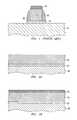
- FIG. 1Such a prior art structure is shown, for example, in FIG. 1 .
- the structure shown in FIG. 1comprises semiconductor substrate 10 , patterned gate dielectric 14 formed on a surface of substrate 10 , patterned polysilicon 16 formed on a portion of patterned gate dielectric 14 , CVD oxide or nitride layer 18 formed atop the patterned polysilicon layer, and sidewall spacers 20 formed on vertical sidewalls of the patterned polysilicon layer and over a portion of the patterned gate dielectric.
- a nitride wet etchcould also attack the vertical gate sidewall or other exposed nitride sidewalls, or the wet may undercut the gate oxide which is present beneath the gate polysilicon, leading to defects in the device.
- One object of the present inventionis to provide a method of reducing the contact resistance in a CMOS device that is formed on a bulk semiconductor substrate or a silicon-on-insulator (SOI) substrate.
- Another object of the present inventionis to provide a method of forming a CMOS device having raised source/drain regions and without increased silicon growth on the gate electrode.
- a yet further object of the present inventionis to provide a method of inhibiting the formation of silicon growth on the gate electrode through surface modification, while requiring only a reduced clean to allow further processing.
- An even further object of the present inventionis to provide a method of forming a CMOS device which includes a step of forming a film on the gate electrode prior to epi silicon growth, wherein the film substantially inhibits the epi silicon growth on the gate without affecting the source/drain regions.
- a still further object of the present inventionis to provide a method of forming a CMOS device which includes a step of modifying at least the top horizontal surface of the gate polysilicon prior to epi growth, wherein the modified surface of the gate polysilicon substantially inhibits the epi silicon growth without affecting the source/drain regions.
- a nitrided surface layeratop the polysilicon gate electrode which inhibits the epitaxial growth of silicon on the polysilicon gate electrode.
- the nitrided surface layeris formed in the present invention by either implanting nitrogen-containing ions into the polysilicon gate electrode or by using a plasma nitridation process that incorporates nitrogen into the polysilicon gate electrode. Both of the above-mentioned techniques modify the top surface of the polysilicon gate electrode in such a manner that inhibits the growth of epitaxial silicon thereon.
- the method of the present inventioncomprises the steps of:
- step (d)forming sidewall spacers on at least exposed vertical sidewalls of said polysilicon layer not removed in step (c) as well as a portion of said gate dielectric layer;
- the present inventionalso includes the step of: (g) removing the nitrided surface layer from said polysilicon layer.
- the nitrided surface layeris formed utilizing a nitrogen ion implantation process. In another embodiment of the present invention, the nitrided surface layer is formed utilizing a plasma nitridation process.
- FIG. 1is a pictorial representation (through a cross-sectional view) of a prior art CMOS device which includes a CVD oxide or nitride formed atop the gate polysilicon prior to growth of the epi silicon layer.
- FIGS. 2A-2Fare pictorial representations (through cross-sectional view) showing the various process steps employed in the present invention.
- the initial structure shown in FIG. 1includes semiconductor substrate 50 , gate dielectric layer 52 formed on semiconductor substrate 50 , and polysilicon layer 54 formed atop gate dielectric layer 52 .
- semiconductor substrate 50includes a silicon-on-insulator (SOI) substrate which comprises a buried oxide region sandwiched between a top Si-containing layer and a bottom Si-containing layer.
- SOIsilicon-on-insulator
- the bottom Si-containing layer, buried oxide region and the top Si-containing layerare not specifically shown in the drawings, but are nevertheless meant to be included within substrate 50 .
- the SOI substrate utilized in the present inventionmay be formed by conventional bonding and cutting processes or by a conventional separation by ion implantation of oxygen (SIMOX) process wherein oxygen ions are implanted into a Si-containing substrate and a high temperature annealing step (1100° C. or above) is used to convert the implanted oxygen ions into a buried oxide region.
- SIMOXseparation by ion implantation of oxygen
- the present inventionalso contemplates the use of bulk semiconductor substrates.
- a bulk substrateany semiconductor material including but not limited to: Si, Ge, SiGe, GaAs, InAs, InP and all other III/V compound semiconductors may be employed in the present invention.
- the present inventionalso contemplates layered semiconductors such as Si/Si or Si/SiGe.
- the bulk semiconductor substratemay be of the n- or p-type depending on the desired device to be fabricated.
- semiconductor substrate 50may contain active device regions, isolation regions or other like regions that are typically present in CMOS containing devices. For clarity, these regions are not shown in the drawings, but are nevertheless meant to be also included within region 50 .
- semiconductor substrate 50is an SOI substrate.
- gate dielectric layer 52which includes an oxide, nitride, oxynitride or any combination or multilayer thereof, is formed on a surface of semiconductor substrate 50 utilizing a conventional process well known in the art.
- the layer of gate dielectric materialmay be formed utilizing a conventional deposition process such as chemical vapor deposition (CVD), plasma-assisted CVD, evaporation or chemical solution deposition, or alternatively the gate dielectric layer may be formed by a thermal growing process such as oxidation, nitridation or oxynitridation.
- gate dielectric layer 52is not critical to the present invention, but typically gate dielectric layer 52 has a thickness of from about 1 to about 20 nm, with a thickness of from about 1.5 to about 10 nm being more highly preferred.
- the gate dielectric material employed in the present inventionmay be a conventional dielectric material such as SiO 2 or Si 3 N 4 , or alternatively high-k dielectrics such as oxides of Ta, Zr, Hf, Al or combinations thereof may be employed.
- gate dielectric layer 52is comprised of an oxide such as SiO 2 , ZrO 2 , HfO 2 , Ta 2 5 or Al 2 O 3 .
- gate dielectric layer 52After forming gate dielectric layer 52 on semiconductor substrate 50 , polysilicon layer 54 is formed atop the gate dielectric layer. Note that the polysilicon layer will subsequently serve as the gate electrode of a metal oxide semiconductor field effect transistor (MOSFET) therefore the polysilicon layer should be a doped polysilicon layer.
- doping of the gate polysiliconmay occur during deposition of the polysilicon layer utilizing a conventional in-situ doping deposition process; after deposition of the polysilicon layer, but prior to etching the gate stack; or after etching the gate stack.
- polysilicon layer 54is formed by a conventional deposition process such as CVD or plasma-assisted CVD and ion implantation is employed in doping the polysilicon layer. Note that the doped polysilicon layer is subjected to a conventional activation annealing process either before or after the gate stack has been etched.
- polysilicon layer 54is not critical to the present invention, but typically polysilicon layer 54 has a thickness of from about 100 to about 200 nm, with a thickness of from about 120 to about 180 nm being more highly preferred.
- nitrided surface layer 56is formed on polysilicon layer 54 .
- nitrided surface layer 56is formed in the present invention by implanting nitrogen ions into the surface of the polysilicon layer; by utilizing a plasma nitridation process; or by utilizing any other technique that is capable of modifying the polysilicon layer by forming a nitrided surface layer thereon.
- the nitrided surface layeris employed in the present invention as a means for inhibiting the growth of epi silicon on the patterned polysilicon gate electrode (to be subsequently formed).
- a nitrogen-containing ion source materialsuch as N 2 , NO, N 2 O, NH 3 and mixtures thereof, is employed and the nitrogen ions from the source material are implanted into the polysilicon layer utilizing an ion dosage of from about 1E14 to about 1E15 atoms/cm 2 and an energy of from about 1 to about 5 Kev.
- This implantcauses portions of the polysilicon layer to become nitrogen rich, yet the implant does not form a continuous layer of stoichiometric silicon nitride film.
- the nitrogen rich surfaceretards the nucleation of the silicon and thus causes little or no silicon epi growth on the polysilicon gate electrode.
- the present inventionalso contemplates nitrogen ion implantation processes wherein the nitrogen-containing ion source material is admixed with an inert gas such as He, Ar, Ne, Kr or Xe.
- an inert gassuch as He, Ar, Ne, Kr or Xe.
- the nitridationis carried out at a temperature of about 1100° C. or below in a nitrogen-containing atmosphere such as N 2 , NO, N 2 O, and NH 3 . Mixtures of the aforementioned nitrogencontaining atmospheres are also contemplated herein.
- the present inventionalso contemplates plasma nitridation processes wherein the nitrogen-containing gas is admixed with an inert gas such as He, Ar, Ne, Kr or Xe. More specifically, the plasma nitridation process is carried out at a temperature of from about 1000° C. to about 1100° C.
- the nitrogen species used in this embodiment of the present inventionwill form ions that react with the silicon surface and form a nitrogen rich surface layer on the polysilicon layer.
- the plasma nitridation processdoes not form a continuous silicon nitride layer, but instead forms a nitrided surface layer on the polysilicon layer that will inhibit the growth of epi silicon layer.
- the plasma nitridation processmay be carried out using furnace heating conditions wherein longer nitridation times (on the order of from about 4 hours or greater) are employed, or the plasma nitridation process may be carried out using rapid thermal conditions wherein shorter heating times (on the order of about 120 seconds or less) are employed.
- RTrapid thermal
- RPMrapid plasma nitridation
- DPNdecoupled plasma nitridation
- the nitrided surface layer formedhas a thickness of from about 0.8 to about 2 nm, with a thickness of from about 1.0 to about 1.5 nm being more highly preferred.
- nitrided surface layer 56 and polysilicon layer 54are patterned utilizing conventional lithography and etching so as to form at least one patterned stack region 58 (includes patterned nitride surface layer 56 and patterned polysilicon layer 54 ) on gate dielectric layer 52 ; See FIG. 2C It is emphasized that although the drawings show the formation of only one patterned stack region, the present invention works equally well when a plurality of patterned stack regions are formed on the gate dielectric layer.
- Patterned stack region 58which includes patterned nitrided surface layer 56 and patterned polysilicon layer 54 , is formed by first applying a photoresist (not shown in the drawings) to a surface of nitrided surface layer 56 , exposing said photoresist to a pattern of radiation and developing the pattern using a conventional resist developer.
- a hardmasksuch as a layer of tetraethylorthosilicate (TEOS) is formed on the nitrided surface layer prior to resist application, exposure and development.
- the stack regionwould include a patterned layer of harkmask material atop the patterned nitrided surface layer.
- a conventional dry etching processsuch as reactive ion etching, plasma etching, ion beam etching or laser ablation is employed in transferring the resist pattern to the underlying nitrided surface layer and polysilicon layer.
- the etching process utilized during this step of the present inventionselectively removes portions of the nitrided surface layer and polysilicon layer that are not protected by the patterned resist, while leaving other portions of the nitrided surface layer and the polysilicon layer protected by the patterned resist on the surface of gate dielectric layer 52 .
- the patterned photoresistis removed from the structure utilizing a conventional stripping process well known in the art so as to provide the structure shown, for example, in FIG. 2 C.
- FIG. 2Dshows the resultant structure after forming sidewall spacers 60 on vertical surfaces of the stack region (including at least patterned polysilicon layer 54 ) as well as on a portion of gate dielectric layer 52 and etching gate dielectric layer 52 that is not protected by either the sidewall spacers or the patterned stack region.
- the sidewall spacerswhich may be composed of an oxide, nitride, oxynitride or combinations and multilayers thereof, are formed utilizing a conventional process well known to those skilled in the art.
- sidewall spacers 60are formed by deposition and etching.
- a highly preferred material for sidewall spacers 60is a nitride such as Si 3 N 4 .
- a conventional etching processsuch as a diluted HF dipping process is used to remove the exposed portions of gate dielectric layer 52 from the structure. Note that a portion of the uppermost surface of semiconductor substrate 50 is exposed following the removal of portions of the gate dielectric layer therefrom.
- source/drain diffusion regions 64are formed into the surface of semiconductor substrate as shown in FIG. 2 D.
- the source/drain regionsare formed utilizing conventional processes well known in the art, including ion implantation and activation annealing. Note that in some embodiments of the present invention, the source/drain regions are formed in the substrate prior to formation of the gate dielectric layer thereon.
- epi silicon layer 62is formed on exposed horizontal surfaces of the structure that do not include the nitrided surface layer. Note that the presence of the nitrided surface layer on the patterned polysilicon gate electrode inhibits the growth of epi silicon layer 62 thereon.
- the epi silicon layeris formed utilizing conventional epitaxial silicon growing process well known in the art. Specifically, the selective epi silicon growth process comprises the use of a silicon-containing source material such as a silane which is deposited at a temperature of about 800° C. or above.
- the thickness of the epi silicon layer formed at this point of the present inventionis not critical to the present invention, but typically epi silicon layer 62 has a thickness of from about 20 to about 40 nm, with a thickness of from about 25 to about 30 nm being more highly preferred.
- FIG. 2Fshows the structure that is formed after nitrided surface layer 56 has been removed from atop the patterned polysilicon gate electrode, i.e., patterned polysilicon layer 54 .
- the nitrided surface layeris removed from atop the patterned polysilicon gate electrode utilizing a conventional dipping, coating or brushing process wherein a chemical etchant that has a high selectively for removing the nitrided surface layer is employed.
- a chemical etchantthat has a high selectively for removing the nitrided surface layer is employed.
- HFcan be employed in removing the nitrided surface layer from atop the patterned polysilicon layer.
- the hardmaskis removed first using a conventional etching process well known in the art and thereafter patterned nitrided surface layer 56 is removed, as indicated above.
- CMOS processes stepsare performed on the structure shown in FIG. 2 F.
- processing steps which form metal silicide contacts on the source and drain regions as well as gate electrodescan be employed in the present invention.
- processing steps that lead to connecting the metal silicide contacts to external wirescan be employed in the present invention as well.
- a key advantage of the inventive methodis that the surface treatment can be performed on only part of the semiconductor substrate, leaving some of the polysilicon untreated. This cases allows certain gate electrodes to grow selective epi thereon, while others that receive the nitrided surface layer do not contain selective epi thereon. This aspect of the present invention could be useful in specific device applications where a thicker polysilicon in certain regions could provide a lower resistance.
Landscapes
- Insulated Gate Type Field-Effect Transistor (AREA)
- Electrodes Of Semiconductors (AREA)
- Thin Film Transistor (AREA)
Abstract
Description
Claims (20)
Priority Applications (2)
| Application Number | Priority Date | Filing Date | Title |
|---|---|---|---|
| US09/882,095US6440807B1 (en) | 2001-06-15 | 2001-06-15 | Surface engineering to prevent EPI growth on gate poly during selective EPI processing |
| US10/183,336US6900092B2 (en) | 2001-06-15 | 2002-06-27 | Surface engineering to prevent epi growth on gate poly during selective epi processing |
Applications Claiming Priority (1)
| Application Number | Priority Date | Filing Date | Title |
|---|---|---|---|
| US09/882,095US6440807B1 (en) | 2001-06-15 | 2001-06-15 | Surface engineering to prevent EPI growth on gate poly during selective EPI processing |
Related Child Applications (1)
| Application Number | Title | Priority Date | Filing Date |
|---|---|---|---|
| US10/183,336DivisionUS6900092B2 (en) | 2001-06-15 | 2002-06-27 | Surface engineering to prevent epi growth on gate poly during selective epi processing |
Publications (1)
| Publication Number | Publication Date |
|---|---|
| US6440807B1true US6440807B1 (en) | 2002-08-27 |
Family
ID=25379879
Family Applications (2)
| Application Number | Title | Priority Date | Filing Date |
|---|---|---|---|
| US09/882,095Expired - LifetimeUS6440807B1 (en) | 2001-06-15 | 2001-06-15 | Surface engineering to prevent EPI growth on gate poly during selective EPI processing |
| US10/183,336Expired - Fee RelatedUS6900092B2 (en) | 2001-06-15 | 2002-06-27 | Surface engineering to prevent epi growth on gate poly during selective epi processing |
Family Applications After (1)
| Application Number | Title | Priority Date | Filing Date |
|---|---|---|---|
| US10/183,336Expired - Fee RelatedUS6900092B2 (en) | 2001-06-15 | 2002-06-27 | Surface engineering to prevent epi growth on gate poly during selective epi processing |
Country Status (1)
| Country | Link |
|---|---|
| US (2) | US6440807B1 (en) |
Cited By (17)
| Publication number | Priority date | Publication date | Assignee | Title |
|---|---|---|---|---|
| US20030089993A1 (en)* | 2001-11-14 | 2003-05-15 | Fujitsu Limited | Semiconductor device including titanium wires and manufacturing method therefor |
| US6794264B2 (en)* | 2000-05-03 | 2004-09-21 | Ibis Technology Corporation | Implantation process using substoichiometric, oxygen doses at different energies |
| US20040248368A1 (en)* | 2002-11-20 | 2004-12-09 | Natzle Wesley C. | Mosfet device with in-situ doped, raised source and drain structures |
| US6881635B1 (en) | 2004-03-23 | 2005-04-19 | International Business Machines Corporation | Strained silicon NMOS devices with embedded source/drain |
| US20050095795A1 (en)* | 2003-07-07 | 2005-05-05 | Yong-Hoon Son | MOS transistors having recesses with elevated source/drain regions and methods of fabricating such transistors |
| US20050142729A1 (en)* | 2003-12-30 | 2005-06-30 | Hyunsoo Shin | Methods for forming a field effect transistor |
| US20060027875A1 (en)* | 2002-08-14 | 2006-02-09 | Samsung Electronics Co., Ltd. | Semiconductor device with gate space of positive slope and fabrication method thereof |
| US20090105050A1 (en)* | 2007-10-17 | 2009-04-23 | Mayo Elvin A | Exercise Machine for Back Rehabilitation |
| US20090152590A1 (en)* | 2007-12-13 | 2009-06-18 | International Business Machines Corporation | Method and structure for semiconductor devices with silicon-germanium deposits |
| US20150072502A1 (en)* | 2012-08-31 | 2015-03-12 | SK Hynix Inc. | Semiconductor device including buried gate, module and system, and method for manufacturing |
| US20150214331A1 (en)* | 2014-01-30 | 2015-07-30 | Globalfoundries Inc. | Replacement metal gate including dielectric gate material |
| US9620619B2 (en)* | 2012-01-12 | 2017-04-11 | Globalfoundries Inc. | Borderless contact structure |
| US9627207B2 (en) | 2014-11-07 | 2017-04-18 | Samsung Electronics Co., Ltd. | Methods of forming semiconductor device having gate electrode |
| US9972672B1 (en) | 2017-01-11 | 2018-05-15 | International Business Machines Corporation | Tunable resistor with curved resistor elements |
| US9991330B1 (en) | 2017-01-11 | 2018-06-05 | International Business Machines Corporation | Resistors with controlled resistivity |
| US10043806B2 (en) | 2015-10-06 | 2018-08-07 | Samsung Electronics Co., Ltd. | Semiconductor devices and methods of manufacturing the same |
| US10283583B2 (en) | 2017-01-11 | 2019-05-07 | International Business Machines Corporation | 3D resistor structure with controlled resistivity |
Families Citing this family (8)
| Publication number | Priority date | Publication date | Assignee | Title |
|---|---|---|---|---|
| US7015534B2 (en)* | 2003-10-14 | 2006-03-21 | Texas Instruments Incorporated | Encapsulated MOS transistor gate structures and methods for making the same |
| DE102005030272A1 (en)* | 2005-06-21 | 2007-01-04 | Hansgrohe Ag | Method for producing decorative surface structures |
| DE102005051819B3 (en)* | 2005-10-28 | 2007-06-14 | Infineon Technologies Ag | Production process for semiconductor structures |
| JP5534715B2 (en)* | 2009-05-27 | 2014-07-02 | 株式会社ジャパンディスプレイ | Defect correction method and apparatus for electronic circuit pattern |
| KR101728141B1 (en)* | 2010-09-29 | 2017-04-18 | 삼성전자 주식회사 | Method for fabricating a semiconductor device using blocking layers |
| CN102655110B (en)* | 2011-03-04 | 2014-10-22 | 中芯国际集成电路制造(上海)有限公司 | SOI (silicon on insulator) transistor and manufacture method thereof |
| WO2020073306A1 (en)* | 2018-10-12 | 2020-04-16 | Boe Technology Group Co., Ltd. | Micro light emitting diode apparatus and fabricating method thereof |
| TWI773873B (en) | 2019-01-22 | 2022-08-11 | 聯華電子股份有限公司 | Semiconductor device and method for fabricating the same |
Citations (11)
| Publication number | Priority date | Publication date | Assignee | Title |
|---|---|---|---|---|
| US5319232A (en) | 1991-11-25 | 1994-06-07 | Motorola, Inc. | Transistor having a lightly doped region |
| US5369049A (en) | 1993-12-17 | 1994-11-29 | International Business Machines Corporation | DRAM cell having raised source, drain and isolation |
| US5384277A (en) | 1993-12-17 | 1995-01-24 | International Business Machines Corporation | Method for forming a DRAM trench cell capacitor having a strap connection |
| US5869375A (en) | 1996-02-05 | 1999-02-09 | Lg Semicon Co., Ltd. | Transistor fabrication method |
| US6083836A (en) | 1997-12-23 | 2000-07-04 | Texas Instruments Incorporated | Transistors with substitutionally formed gate structures and method |
| US6083798A (en) | 1998-05-26 | 2000-07-04 | Advanced Micro Devices, Inc. | Method of producing a metal oxide semiconductor device with raised source/drain |
| US6087235A (en) | 1999-10-14 | 2000-07-11 | Advanced Micro Devices, Inc. | Method for effective fabrication of a field effect transistor with elevated drain and source contact structures |
| US6156613A (en) | 1998-03-02 | 2000-12-05 | Texas Instruments - Acer Incorporated | Method to form MOSFET with an elevated source/drain |
| US6160299A (en) | 1997-08-29 | 2000-12-12 | Texas Instruments Incorporated | Shallow-implant elevated source/drain doping from a sidewall dopant source |
| US6174754B1 (en) | 2000-03-17 | 2001-01-16 | Taiwan Semiconductor Manufacturing Company | Methods for formation of silicon-on-insulator (SOI) and source/drain-on-insulator(SDOI) transistors |
| US6177323B1 (en) | 1998-03-02 | 2001-01-23 | Texas Instruments - Acer Incorporated | Method to form MOSFET with an elevated source/drain for PMOSFET |
Family Cites Families (5)
| Publication number | Priority date | Publication date | Assignee | Title |
|---|---|---|---|---|
| US4714685A (en) | 1986-12-08 | 1987-12-22 | General Motors Corporation | Method of fabricating self-aligned silicon-on-insulator like devices |
| US4998150A (en) | 1988-12-22 | 1991-03-05 | Texas Instruments Incorporated | Raised source/drain transistor |
| US5118639A (en)* | 1990-05-29 | 1992-06-02 | Motorola, Inc. | Process for the formation of elevated source and drain structures in a semiconductor device |
| US5250454A (en) | 1992-12-10 | 1993-10-05 | Allied Signal Inc. | Method for forming thickened source/drain contact regions for field effect transistors |
| US6100188A (en)* | 1998-07-01 | 2000-08-08 | Texas Instruments Incorporated | Stable and low resistance metal/barrier/silicon stack structure and related process for manufacturing |
- 2001
- 2001-06-15USUS09/882,095patent/US6440807B1/ennot_activeExpired - Lifetime
- 2002
- 2002-06-27USUS10/183,336patent/US6900092B2/ennot_activeExpired - Fee Related
Patent Citations (11)
| Publication number | Priority date | Publication date | Assignee | Title |
|---|---|---|---|---|
| US5319232A (en) | 1991-11-25 | 1994-06-07 | Motorola, Inc. | Transistor having a lightly doped region |
| US5369049A (en) | 1993-12-17 | 1994-11-29 | International Business Machines Corporation | DRAM cell having raised source, drain and isolation |
| US5384277A (en) | 1993-12-17 | 1995-01-24 | International Business Machines Corporation | Method for forming a DRAM trench cell capacitor having a strap connection |
| US5869375A (en) | 1996-02-05 | 1999-02-09 | Lg Semicon Co., Ltd. | Transistor fabrication method |
| US6160299A (en) | 1997-08-29 | 2000-12-12 | Texas Instruments Incorporated | Shallow-implant elevated source/drain doping from a sidewall dopant source |
| US6083836A (en) | 1997-12-23 | 2000-07-04 | Texas Instruments Incorporated | Transistors with substitutionally formed gate structures and method |
| US6156613A (en) | 1998-03-02 | 2000-12-05 | Texas Instruments - Acer Incorporated | Method to form MOSFET with an elevated source/drain |
| US6177323B1 (en) | 1998-03-02 | 2001-01-23 | Texas Instruments - Acer Incorporated | Method to form MOSFET with an elevated source/drain for PMOSFET |
| US6083798A (en) | 1998-05-26 | 2000-07-04 | Advanced Micro Devices, Inc. | Method of producing a metal oxide semiconductor device with raised source/drain |
| US6087235A (en) | 1999-10-14 | 2000-07-11 | Advanced Micro Devices, Inc. | Method for effective fabrication of a field effect transistor with elevated drain and source contact structures |
| US6174754B1 (en) | 2000-03-17 | 2001-01-16 | Taiwan Semiconductor Manufacturing Company | Methods for formation of silicon-on-insulator (SOI) and source/drain-on-insulator(SDOI) transistors |
Cited By (31)
| Publication number | Priority date | Publication date | Assignee | Title |
|---|---|---|---|---|
| US6794264B2 (en)* | 2000-05-03 | 2004-09-21 | Ibis Technology Corporation | Implantation process using substoichiometric, oxygen doses at different energies |
| US20030089993A1 (en)* | 2001-11-14 | 2003-05-15 | Fujitsu Limited | Semiconductor device including titanium wires and manufacturing method therefor |
| US7372157B2 (en)* | 2001-11-14 | 2008-05-13 | Fujitsu Limited | Semiconductor device including titanium wires and manufacturing method therefor |
| US20060027875A1 (en)* | 2002-08-14 | 2006-02-09 | Samsung Electronics Co., Ltd. | Semiconductor device with gate space of positive slope and fabrication method thereof |
| US7566924B2 (en)* | 2002-08-14 | 2009-07-28 | Samsung Electronics Co., Ltd. | Semiconductor device with gate spacer of positive slope and fabrication method thereof |
| US20040248368A1 (en)* | 2002-11-20 | 2004-12-09 | Natzle Wesley C. | Mosfet device with in-situ doped, raised source and drain structures |
| US6858903B2 (en)* | 2002-11-20 | 2005-02-22 | International Business Machines Corporation | MOSFET device with in-situ doped, raised source and drain structures |
| US8039350B2 (en) | 2003-07-07 | 2011-10-18 | Samsung Electronics Co., Ltd. | Methods of fabricating MOS transistors having recesses with elevated source/drain regions |
| US20050095795A1 (en)* | 2003-07-07 | 2005-05-05 | Yong-Hoon Son | MOS transistors having recesses with elevated source/drain regions and methods of fabricating such transistors |
| US7683405B2 (en) | 2003-07-07 | 2010-03-23 | Samsung Electronics Co., Ltd. | MOS transistors having recesses with elevated source/drain regions |
| US8304318B2 (en) | 2003-07-07 | 2012-11-06 | Samsung Electronics Co., Ltd. | Methods of fabricating MOS transistors having recesses with elevated source/drain regions |
| US20050142729A1 (en)* | 2003-12-30 | 2005-06-30 | Hyunsoo Shin | Methods for forming a field effect transistor |
| US7402484B2 (en)* | 2003-12-30 | 2008-07-22 | Dongbu Electronics Co., Ltd. | Methods for forming a field effect transistor |
| US6881635B1 (en) | 2004-03-23 | 2005-04-19 | International Business Machines Corporation | Strained silicon NMOS devices with embedded source/drain |
| US20090105050A1 (en)* | 2007-10-17 | 2009-04-23 | Mayo Elvin A | Exercise Machine for Back Rehabilitation |
| US20090152590A1 (en)* | 2007-12-13 | 2009-06-18 | International Business Machines Corporation | Method and structure for semiconductor devices with silicon-germanium deposits |
| US9620619B2 (en)* | 2012-01-12 | 2017-04-11 | Globalfoundries Inc. | Borderless contact structure |
| US9418854B2 (en)* | 2012-08-31 | 2016-08-16 | SK Hynix Inc. | Semiconductor device including buried gate, module and system, and method for manufacturing |
| US20150072502A1 (en)* | 2012-08-31 | 2015-03-12 | SK Hynix Inc. | Semiconductor device including buried gate, module and system, and method for manufacturing |
| US20150214331A1 (en)* | 2014-01-30 | 2015-07-30 | Globalfoundries Inc. | Replacement metal gate including dielectric gate material |
| US9627207B2 (en) | 2014-11-07 | 2017-04-18 | Samsung Electronics Co., Ltd. | Methods of forming semiconductor device having gate electrode |
| US10043806B2 (en) | 2015-10-06 | 2018-08-07 | Samsung Electronics Co., Ltd. | Semiconductor devices and methods of manufacturing the same |
| US10411011B2 (en) | 2015-10-06 | 2019-09-10 | Samsung Electronics Co., Ltd. | Semiconductor devices and methods of manufacturing the same |
| US9972672B1 (en) | 2017-01-11 | 2018-05-15 | International Business Machines Corporation | Tunable resistor with curved resistor elements |
| US20180197938A1 (en)* | 2017-01-11 | 2018-07-12 | International Business Machines Corporation | Tunable resistor with curved resistor elements |
| US10211280B2 (en)* | 2017-01-11 | 2019-02-19 | International Business Machines Corporation | Method of forming tunable resistor with curved resistor elements |
| US10211279B2 (en) | 2017-01-11 | 2019-02-19 | International Business Machines Corporation | Tunable resistor with curved resistor elements |
| US10217809B2 (en) | 2017-01-11 | 2019-02-26 | International Business Machines Corporation | Method of forming resistors with controlled resistivity |
| US10283583B2 (en) | 2017-01-11 | 2019-05-07 | International Business Machines Corporation | 3D resistor structure with controlled resistivity |
| US10325978B2 (en) | 2017-01-11 | 2019-06-18 | International Business Machines Corporation | Resistors with controlled resistivity |
| US9991330B1 (en) | 2017-01-11 | 2018-06-05 | International Business Machines Corporation | Resistors with controlled resistivity |
Also Published As
| Publication number | Publication date |
|---|---|
| US6900092B2 (en) | 2005-05-31 |
| US20020192888A1 (en) | 2002-12-19 |
Similar Documents
| Publication | Publication Date | Title |
|---|---|---|
| US6440807B1 (en) | Surface engineering to prevent EPI growth on gate poly during selective EPI processing | |
| US6080682A (en) | Methodology for achieving dual gate oxide thicknesses | |
| US7446005B2 (en) | Manufacturable recessed strained RSD structure and process for advanced CMOS | |
| US6686245B1 (en) | Vertical MOSFET with asymmetric gate structure | |
| US6475888B1 (en) | Method for forming ultra-shallow junctions using laser annealing | |
| US7569466B2 (en) | Dual metal gate self-aligned integration | |
| US6136674A (en) | Mosfet with gate plug using differential oxide growth | |
| US20070275532A1 (en) | Optimized deep source/drain junctions with thin poly gate in a field effect transistor | |
| US20090001468A1 (en) | Method of fabricating transistor including buried insulating layer and transistor fabricated using the same | |
| KR100550196B1 (en) | How to improve gate activation by employing atomic oxygen oxidation | |
| US6514843B2 (en) | Method of enhanced oxidation of MOS transistor gate corners | |
| US7485516B2 (en) | Method of ion implantation of nitrogen into semiconductor substrate prior to oxidation for offset spacer formation | |
| JP4514023B2 (en) | Silicon oxide liner ion implantation to prevent dopants from diffusing out of source / drain extensions | |
| US6864149B2 (en) | SOI chip with mesa isolation and recess resistant regions | |
| US6635517B2 (en) | Use of disposable spacer to introduce gettering in SOI layer | |
| JP3874716B2 (en) | Manufacturing method of semiconductor device | |
| US6432781B2 (en) | Inverted MOSFET process | |
| US20100032813A1 (en) | Ic formed with densified chemical oxide layer | |
| US20110001197A1 (en) | Method for manufacturing semiconductor device and semiconductor device | |
| US6949471B2 (en) | Method for fabricating poly patterns | |
| US6743690B2 (en) | Method of forming a metal-oxide semiconductor transistor | |
| JP2000077429A (en) | Manufacture of semiconductor device | |
| JP2000311861A (en) | Selective growth method of semiconductor film and method of manufacturing semiconductor device | |
| JP3455742B2 (en) | Semiconductor device | |
| JP2008198786A (en) | Manufacturing method of semiconductor device |
Legal Events
| Date | Code | Title | Description |
|---|---|---|---|
| AS | Assignment | Owner name:INTERNATIONAL BUSINESS MACHINES CORPORATION, NEW Y Free format text:ASSIGNMENT OF ASSIGNORS INTEREST;ASSIGNORS:AJMERA, ATUL C.;SCHEPIS, DOMINIC J.;STEIGERWALT, MICHAEL D.;REEL/FRAME:011914/0288 Effective date:20010608 | |
| STCF | Information on status: patent grant | Free format text:PATENTED CASE | |
| FPAY | Fee payment | Year of fee payment:4 | |
| FPAY | Fee payment | Year of fee payment:8 | |
| REMI | Maintenance fee reminder mailed | ||
| FPAY | Fee payment | Year of fee payment:12 | |
| SULP | Surcharge for late payment | Year of fee payment:11 | |
| AS | Assignment | Owner name:GLOBALFOUNDRIES U.S. 2 LLC, NEW YORK Free format text:ASSIGNMENT OF ASSIGNORS INTEREST;ASSIGNOR:INTERNATIONAL BUSINESS MACHINES CORPORATION;REEL/FRAME:036550/0001 Effective date:20150629 | |
| AS | Assignment | Owner name:GLOBALFOUNDRIES INC., CAYMAN ISLANDS Free format text:ASSIGNMENT OF ASSIGNORS INTEREST;ASSIGNORS:GLOBALFOUNDRIES U.S. 2 LLC;GLOBALFOUNDRIES U.S. INC.;REEL/FRAME:036779/0001 Effective date:20150910 | |
| AS | Assignment | Owner name:WILMINGTON TRUST, NATIONAL ASSOCIATION, DELAWARE Free format text:SECURITY AGREEMENT;ASSIGNOR:GLOBALFOUNDRIES INC.;REEL/FRAME:049490/0001 Effective date:20181127 | |
| AS | Assignment | Owner name:GLOBALFOUNDRIES U.S. INC., CALIFORNIA Free format text:ASSIGNMENT OF ASSIGNORS INTEREST;ASSIGNOR:GLOBALFOUNDRIES INC.;REEL/FRAME:054633/0001 Effective date:20201022 | |
| AS | Assignment | Owner name:GLOBALFOUNDRIES INC., CAYMAN ISLANDS Free format text:RELEASE BY SECURED PARTY;ASSIGNOR:WILMINGTON TRUST, NATIONAL ASSOCIATION;REEL/FRAME:054636/0001 Effective date:20201117 | |
| AS | Assignment | Owner name:GLOBALFOUNDRIES U.S. INC., NEW YORK Free format text:RELEASE BY SECURED PARTY;ASSIGNOR:WILMINGTON TRUST, NATIONAL ASSOCIATION;REEL/FRAME:056987/0001 Effective date:20201117 |